

V
查询2N7000KL供应商
2N7000KL/BS170KL
PRODUCT SUMMARY
V
DS
60
S
G
D
(V)
2 @ VGS = 10 V
4 @ VGS = 4.5 V
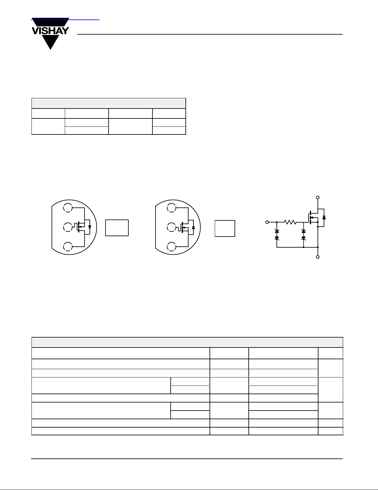
TO-226AA
(TO-92)
1
2
3
r
DS(on)
(W)
“S” = Siliconix Logo
xxyy = Date Code
New Product
N-Channel 60-V (D-S) MOSFET
FEATURES
D TrenchFETr Power MOSFET
V
GS(th)
1.0 to 2.5
Device Marking
Front View
“S” 2N
7000KL
xxyy
(V) I
(TO-18 Lead Form)
D
G
S
(A)
D
0.47
0.33
TO-92-18RM
1
2
3
D ESD Protected: 2000 V
APPLICATIONS
D Direct Logic-Level Interface: TTL/CMOS
D Soild State Relays
D Drivers: Relays, Solenoids, Lamps, Hammers,
Displays, Memories, Transistors, etc.
D Battery Operated Systems
Device Marking
Front View
“S” BS
170KL
xxyy
“S” = Siliconix Logo
xxyy = Date Code
Vishay Siliconix
D
100 W
G
Top View
Ordering Information: 2N7000KL-TR1
Ordering Information: BS170KL-TR1
Top View
ABSOLUTE MAXIMUM RATINGS (TA = 25_C UNLESS OTHERWISE NOTED)
Parameter Symbol Limit Unit
Drain-Source Voltage V
Gate-Source Voltage V
Continuous Drain Current (TJ = 150_C)
Pulsed Drain Current
Power Dissipation
Maximum Junction-to-Ambient R
Operating Junction and Storage Temperature Range TJ, T
a
_
TA = 25_C
TA = 70_C
TA = 25_C
TA = 70_C
I
I
DM
P
thJA
DS
GS
D
D
stg
−55 to 150
60
"20
0.47
0.37
1.0
0.8
0.51
156
S
A
W
_C/W
_C
Notes
a. Pulse width limited by maximum junction temperature.
Document Number: 72705
S-40247—Rev. A, 16-Feb-04
www.vishay.com
1
2N7000KL/BS170KL
b
b
ID ^ 0.25 A
ID ^
V
= 10V
T
Off Ti
g
Vishay Siliconix
New Product
SPECIFICATIONSa (TA = 25_C UNLESS OTHERWISE NOTED)
Parameter Symbol Test Conditions Min Typ Max Unit
Static
Drain-Source Breakdown Voltage V
Gate-Threshold Voltage V
Gate-Body Leakage I
Zero Gate Voltage Drain Current I
On-State Drain Current
Drain-Source On-Resistance
Forward Transconductance
Diode Forward Voltage V
Dynamic
b
b
r
(BR)DSS
GS(th)
GSS
DSS
I
D(on)
DS(on)
g
fs
SD
VGS = 0 V, ID = 10 mA
VDS = VGS, ID = 250 mA
VDS = 0 V, VGS = "10 V "1
VDS = 60 V, VGS = 0 V 1
VDS = 60 V, VGS = 0 V, TJ = 55_C
VGS = 10 V, VDS = 7.5 V 0.8
VGS = 4.5 V, VDS = 10 V 0.5
VGS = 10 V, ID = 0.5 A 1.1 2
VGS = 4.5 V, ID = 0.2 A 1.6 4
VDS = 10 V, ID = 0.5 A 550 mS
IS = 0.3 A, VGS = 0 V 0.87 1.3 V
Limits
60
1 2.0 2.5
V
mA
10
mA
A
W
Total Gate Charge Q
Gate-Source Charge Q
Gate-Drain Charge Q
Gate Resistance R
Turn-On Time
-
urn-
me
Notes
a. Pulse test: PW v300 ms duty cycle v2%.
b. Guaranteed by design, not subject to production testing.
t
d(on)
t
d(off)
g
gs
gd
g
t
r
t
f
VDS = 10 V, VGS = 4.5 V
^ 0.25 A
I
D
VDD = 30 V, RL = 150 W
0.2 A,
Rg = 10 W
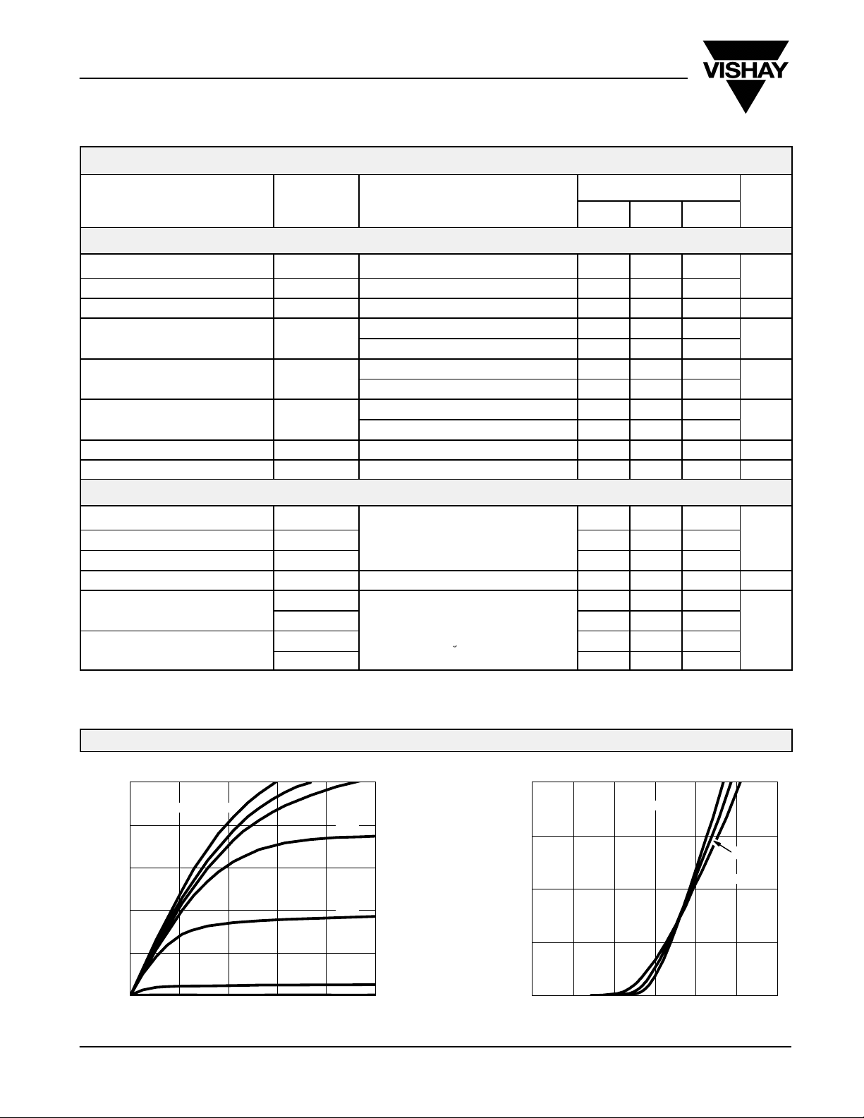
TYPICAL CHARACTERISTICS (25_C UNLESS NOTED)
1.0
0.8
0.6
0.4
− Drain Current (A)I
D
0.2
0.0
012345
Output Characteristics Transfer Characteristics
VGS = 10, 7 V
VDS − Drain-to-Source Voltage (V)
6 V
5 V
4 V
3 V
GEN
0.4 0.6
0.11
0.15
173
3.8 10
4.8 15
12.8 20
9.6 15
1.2
TJ = −55_C
0.9
0.6
− Drain Current (A)I
D
0.3
0
0123456
VGS − Gate-to-Source Voltage (V)
nC
W
ns
25_C
125_C
www.vishay.com
2
Document Number: 72705
S-40247—Rev. A, 16-Feb-04

2N7000KL/BS170KL
New Product
TYPICAL CHARACTERISTICS (25_C UNLESS NOTED)
On-Resistance vs. Drain Current
VGS = 4.5 V
VGS = 10 V
0.0 0.2 0.4 0.6 0.8 1.0
ID − Drain Current (mA)
Gate Charge
W )
− On-Resistance (r
DS(on)
4.0
3.5
3.0
2.5
2.0
1.5
1.0
0.5
0.0
7
Vishay Siliconix
40
32
24
16
C − Capacitance (pF)
8
0
0 5 10 15 20 25
On-Resistance vs. Junction Temperature
2.0
Capacitance
V
= 0 V
GS
C
iss
C
oss
C
rss
VDS − Drain-to-Source Voltage (V)
VDS = 10 V
− Gate-to-Source Voltage (V)
GS
V
6
5
4
3
2
1
0
= 250 mA
I
D
0.0 0.1 0.2 0.3 0.4 0.5 0.6
Qg − Total Gate Charge (nC)
Source-Drain Diode Forward Voltage
1000
VGS = 0 V
100
TJ = 125_C
10
− Source Current (A)I
S
TJ = 25_C
TJ = −55_C
1.6
1.2
− On-Resiistance
(Normalized)
0.8
DS(on)
r
0.4
0.0
−50 −25 0 25 50 75 100 125 150
5
4
W )
3
2
− On-Resistance (r
1
DS(on)
VGS = 10 V @ 500 mA
VGS = 4.5 V
@ 200 mA
TJ − Junction Temperature (_C)
On-Resistance vs. Gate-Source Voltage
ID = 500 mA
ID = 200 mA
1
0.00 0.3 0.6 0.9
VSD − Source-to-Drain Voltage (V)
Document Number: 72705
S-40247—Rev. A, 16-Feb-04
1.2 1.5
0
0246810
VGS − Gate-to-Source Voltage (V)
www.vishay.com
3

2N7000KL/BS170KL
Vishay Siliconix
New Product
TYPICAL CHARACTERISTICS (25_C UNLESS NOTED)
Threshold Voltage Variance Over Temperature
0.4
0.2
ID = 250 mA
−0.0
Variance (V)V
−0.2
GS(th)
−0.4
−0.6
−0.8
−50 −25 0 25 50 75 100 125 150
− Junction Temperature (_C)
T
J
10
Limited by r
1
Safe Operating Area
I
Limited
DM
DS(on)
20
16
12
Power (W)
8
4
0
0.01
Single Pulse Power, Junction-to-Ambient
TA = 25_C
1
Time (sec)
10
100 6000.1
2
1
0.1
Thermal Impedance
Normalized Effective Transient
0.01
10
Duty Cycle = 0.5
0.2
0.1
0.05
0.02
Single Pulse
−4
1 ms
10 ms
0.1
− Drain Current (A)I
D
0.01
I
D(on)
Limited
TA = 25_C
Single Pulse
BV
DSS
Limited
100 ms
1 s
10 s
dc
0.001
0.1 1 10 100
VDS − Drain-to-Source Voltage (V)
Normalized Thermal Transient Impedance, Junction-to-Ambient
Notes:
P
DM
t
1
t
2
t
thJA
thJA
100
1
t
2
=350_C/W
(t)
1. Duty Cycle, D =
2. Per Unit Base = R
3. TJM − TA = PDMZ
4. Surface Mounted
−3
10
−2
10
−1
1 10 60010
Square Wave Pulse Duration (sec)
www.vishay.com
4
Document Number: 72705
S-40247—Rev. A, 16-Feb-04
 Loading...