

Bulletin PD-20517 rev. H 07/04
15MQ040N
SCHOTTKY RECTIFIER
Major Ratings and Characteristics
Characteristics 15MQ040N Units
IFDC 3 A
V
RRM
I
@ tp = 5 µs sine 330 A
FSM
VF@ 2Apk, TJ=125°C 0.43 V
TJrange - 40 to 150 °C
40 V
3 Amp
I
= 3 Amp
F(AV)
VR = 40V
Description/ Features
The 15MQ040N Schottky rectifier is designed to be used for
low-power applications where a reverse voltage of 40 volts is
ancountered and surface mountable is required.
Applications
Switching power supplies
Meter protection
Reverse protection for power input to PC board circuits
Battery isolation and charging
Low threshold voltage diode
Free-wheeling or by-pass diode
Low voltage clamp
Features
Surface mountable
Extremely low forward voltage
Improved reverse blocking voltage capability relative
to other similar size Schottky
Compact size
www.irf.com
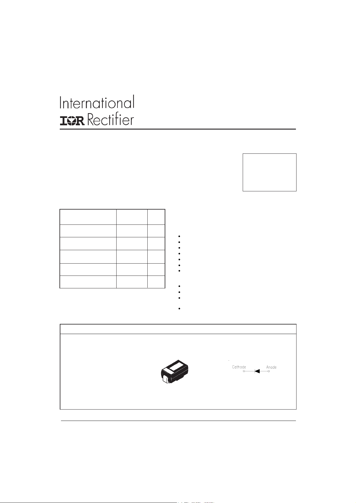
Case Styles
15MQ040N
SMA
1
15MQ040N
Bulletin PD-20517 rev. H 07/04
Voltage Ratings
Part number 15MQ040N
VRMax. DC Reverse Voltage (V)
V
Max. Working Peak Reverse Voltage (V)
RWM
40
Absolute Maximum Ratings
Parameters 15MQ Units Conditions
I
Max. Average Forward Current 2.1 A 50% duty cycle @ TL = 105 °C, rectangular wave form.
F(AV)
* See Fig. 4 On PC board 9mm2 island(.013mm thick copper pad area)
I
Max. Peak One Cycle Non-Repetitive 330 5µs Sine or 3µs Rect. pulse
FSM
A
Surge Current * See Fig. 6 140 10ms Sine or 6ms Rect. pulse
EASNon-Repetitive Avalanche Energy 6.0 mJ TJ = 25 °C, IAS = 1A, L = 12mH
IARRepetitive Avalanche Current 1.0 A
Following any rated
load condition and
with rated V
RRM
Electrical Specifications
Parameters 15MQ Units Conditions
VFMMax. Forward Voltage Drop (1) 0.42 V @ 1A
* See Fig. 1 0.49 V @ 2A
0.34 V @ 1A
0.43 V @ 2A
IRMMax. Reverse Leakage Current (1) 0.5 mA TJ = 25 °C
* See Fig. 2 20 mA TJ = 125 °C
V
Threshold Voltage 0.26 V TJ = TJ max.
F(TO)
rtForward Slope Resistance 64.6 m Ω
CTTypical Junction Capacitance 134 pF VR = 10VDC, TJ = 25°C, test signal = 1Mhz
LSTypical Series Inductance 2.0 nH Measured lead to lead 5mm from package body
dv/dt Max. Voltage Rate of Change 10000 V/µs (Rated VR)
(1) Pulse Width < 300µs, Duty Cycle < 2%
TJ = 25 °C
TJ = 125 °C
VR = rated V
R
applied
Thermal-Mechanical Specifications
Parameters 15MQ Units Conditions
TJMax. Junction Temperature Range (*) -40 to 150 °C
T
Max. Storage Temperature Range -40 to 150 °C
stg
R
Max. Thermal Resistance Junction 80 °C/W DC operation
thJA
to Ambient
wt Approximate Weight 0.07(0.002) g (oz.)
Case Style SMA Similar D-64
Device Marking IR3F
(*) dPtot 1
< thermal runaway condition for a diode on its own heatsink
dTj Rth( j-a)
2 www.irf.com

15MQ040N
Bulletin PD-20517 rev. H 07/04
100
T = 150°C
10
R
Re verse Current - I (m A)
0.01
F
T = 150°C
J
T = 125°C
J
1
T = 25°C
J
0.001
J
10
1
125°C
100°C
75°C
0.1
50°C
25°C
0 5 10 15 20 25 30 35 40
Reverse Voltage - V (V)
R
Fig. 2 - Typical Peak Reverse Current
Vs. Reverse Voltage
Instantaneous Forward Current - I (A)
1000
T
T = 2 5 °C
J
100
0.1
0.20.30.40.50.60.70.80.9
Forwa rd Voltag e Drop - V (V)
FM
Fig. 1 - Maximum Forward Voltage Drop Characteristics
Junction Cap ac itance - C (pF)
10
0 5 10 15 20 25 30 35 40 45
Reverse Voltag e - V (V)
R
Fig. 3 - Typical Junction Capacitance
Vs. Reverse Voltage
www.irf.com 3

15MQ040N
Bulletin PD-20517 rev. H 07/04
150
140
130
120
110
100
D = 0.20
D = 0.25
90
D = 0.33
80
D = 0.50
D = 0.75
70
60
Sq ua re wa ve (D = 0.50)
80% Rat ed V a pplied
50
Allowable Case Temperature - (°C)
40
se e no te (2 )
30
00.511.522.53
R
Ave rag e Forwa rd C urrent - I (A)
Fig. 4 - Maximum Average Forward Current
Vs. Allowable Lead Temperature
1000
FSM
DC
F( A V )
At Any Ra ted Load Cond it ion
And With Rat ed V Ap plied
Fo ll o w in g Surg e
RRM
1.6
D = 0.20
1.4
D = 0.25
D = 0.33
1.2
D = 0.50
D = 0.75
1
0.8
RM S Li m it
DC
0.6
0.4
Average Power Loss - (Watts)
0.2
0
00.511.522.53
Ave rag e Forwa rd C urrent - I (A)
F( A V )
Fig. 5 - Maximum Average Forward Dissipation
Vs. Average Forward Current
Non-Repe tit ive Surge C urrent - I (A)
100
10 100 1000 10000
Sq ua re Wav e Pulse Durat ion - t (m ic rosec )
p
Fig. 6 - Maximum Peak Surge Forward Current Vs. Pulse Duration
(2) Formula used: TC = TJ - (Pd + Pd
Pd = Forward Power Loss = I
Pd
= Inverse Power Loss = VR1 x IR (1 - D); IR @ V
REV
F(AV)
) x R
REV
x VFM @ (I
thJC
;
F(AV)
/ D) (see Fig. 6);
= 80% rated V
R1
R
4 www.irf.com

Outline Table
Device Marking: IR3F
15MQ040N
Bulletin PD-20517 rev. H 07/04
CATHODE ANODE
1.40 (.055)
1.60 (.062)
2.00 (.078)
2.44 (.096)
0.76 (.030)
1.52 (.060)
4.00 (.157)
4.60 (.181)
4.80 (.188)
5.28 (.208)
2.50 (.098)
2.90 (.114)
.152 (.006)
.305 (.012)
.103 (.004)
.203 (.008)
Outline SMA
1 2
1.47 MIN.
SOLDERING PAD
2
2.10 MAX.
(.085 MAX. )
5.53 (.218)
POLARITY PART NU MBER
1
(.058 MIN.)
1.27 MIN.
(.050 MIN.)
Dimensions in millimeters and (inches)
For recommended footprint and soldering techniques refer to application note #AN-994
Marking & Identification
Each device has 2 rows for identification. The first row designates the device as manufactured by International
Rectifier, indicated by the letters "IR", and the Part Number (indicates the current, the voltage rating and
Schottky Generation). The second row indicates the year, the week of manufacturing and the Site ID.
IR3F
VOLTAGE
CURRENT
IR LOGO
YYWWX
SITE ID
WEEK
2nd digit of the YEAR
"Y" = 1st digit of the YEAR "standard product"
"P" = "Lead-Free"
www.irf.com 5

15MQ040N
Bulletin PD-20517 rev. H 07/04
Tape & Reel Information
Ordering Information Table
Dimensions in millimetres and (inches)
Device Code
15 M Q 040 N TR -
24
1
1 - Current Rating
2 - M = SMA
3 - Q = Schottky Q Series
4 - Voltage Rating (040 = 40V)
5 - N = New SMA
6 - y none = Box (1000 pieces)
3
5
y TR = Tape & Reel (7500 pieces)
7 y none = Standard Production
y PbF = Lead-Free
This product has been designed and qualified for Industrial Level.
Data and specifications subject to change without notice.
Qualification Standards can be found on IR's Web site.
7
6
IR WORLD HEADQUARTERS: 233 Kansas St., El Segundo, California 90245, USA Tel: (310) 252-7105
Visit us at www.irf.com for sales contact information. 07/04
TAC Fax: (310) 252-7309
6 www.irf.com
 Loading...