

Anode
1
2
3
Cathode
TO-220AC
Base
cathode
10ETS08PbF, 10ETS12PbF High Voltage Series
Vishay Semiconductors
Input Rectifier Diode, 10 A
FEATURES
• Compliant to RoHS directive 2002/95/EC
• Designed and qualified for industrial level
APPLICATIONS
• Input rectification
• Vishay Semiconductors switches and output rectifiers
which are available in identical package outlines
PRODUCT SUMMARY
VF at 10 A < 1.1 V
I
FSM
V
RRM
200 A
800 V/1200 V
DESCRIPTION
The 10ETS..PbF rectifier series has been optimized for very
low forward voltage drop, with moderate leakage.
The glass passivation technology used has reliable
operation up to 150 °C junction temperature.
OUTPUT CURRENT IN TYPICAL APPLICATIONS
APPLICATIONS SINGLE-PHASE BRIDGE THREE-PHASE BRIDGE UNITS
Capacitive input filter T
common heatsink of 1 °C/W
= 55 °C, TJ = 125 °C
A
12.0 16.0 A
MAJOR RATINGS AND CHARACTERISTICS
SYMBOL CHARACTERISTICS VALUES UNITS
I
F(AV)
V
I
FSM
V
T
RRM
F
J
Sinusoidal waveform 10 A
800/1200 V
200 A
10 A, TJ = 25 °C 1.1 V
- 40 to 150 °C
VOLTAGE RATINGS
V
, MAXIMUM PEAK
PART NUMBER
10ETS08PbF 800 900
10ETS12PbF 1200 1300
RRM
REVERSE VOLTAGE
V
V
, MAXIMUM NON-REPETITIVE
RSM
PEAK REVERSE VOLTAGE
V
I
RRM
AT 150 °C
mA
0.5
ABSOLUTE MAXIMUM RATINGS
PARAMETER SYMBOL TEST CONDITIONS VALUES UNITS
Maximum average forward current I
Maximum peak one cycle
non-repetitive surge current
Maximum I
Maximum I
* Pb containing terminations are not RoHS compliant, exemptions may apply
Document Number: 94337 For technical questions within your region, please contact one of the following: www.vishay.com
Revision: 22-Jul-10 DiodesAmericas@vishay.com
2
t for fusing I2t
2
t for fusing I2t t = 0.1 ms to 10 ms, no voltage reapplied 1450 A2s
F(AV)
I
FSM
TC = 105 °C, 180° conduction half sine wave 10
10 ms sine pulse, rated V
10 ms sine pulse, no voltage reapplied 200
10 ms sine pulse, rated V
10 ms sine pulse, no voltage reapplied 145
, DiodesAsia@vishay.com, DiodesEurope@vishay.com 1
applied 170
RRM
applied 130
RRM
A
2
A
s
10ETS08PbF, 10ETS12PbF High Voltage Series
Vishay Semiconductors
Input Rectifier Diode, 10 A
ELECTRICAL SPECIFICATIONS
PARAMETER SYMBOL TEST CONDITIONS VALUES UNITS
Maximum forward voltage drop V
Forward slope resistance r
Threshold voltage V
Maximum reverse leakage current I
FM
F(TO)
RM
10 A, TJ = 25 °C 1.1 V
t
TJ = 150 °C
TJ = 25 °C
T
= 150 °C 0.50
J
V
= Rated V
R
RRM
20 m
0.82 V
0.05
THERMAL - MECHANICAL SPECIFICATIONS
PARAMETER SYMBOL TEST CONDITIONS VALUES UNITS
Maximum junction and storage temperature range T
Maximum thermal resistance, junction to case R
Maximum thermal resistance, junction to ambient
(PCB mount)
Soldering temperature T
, T
J
Stg
DC operation 2.5
thJC
(1)
R
62
thJA
S
Approximate weight
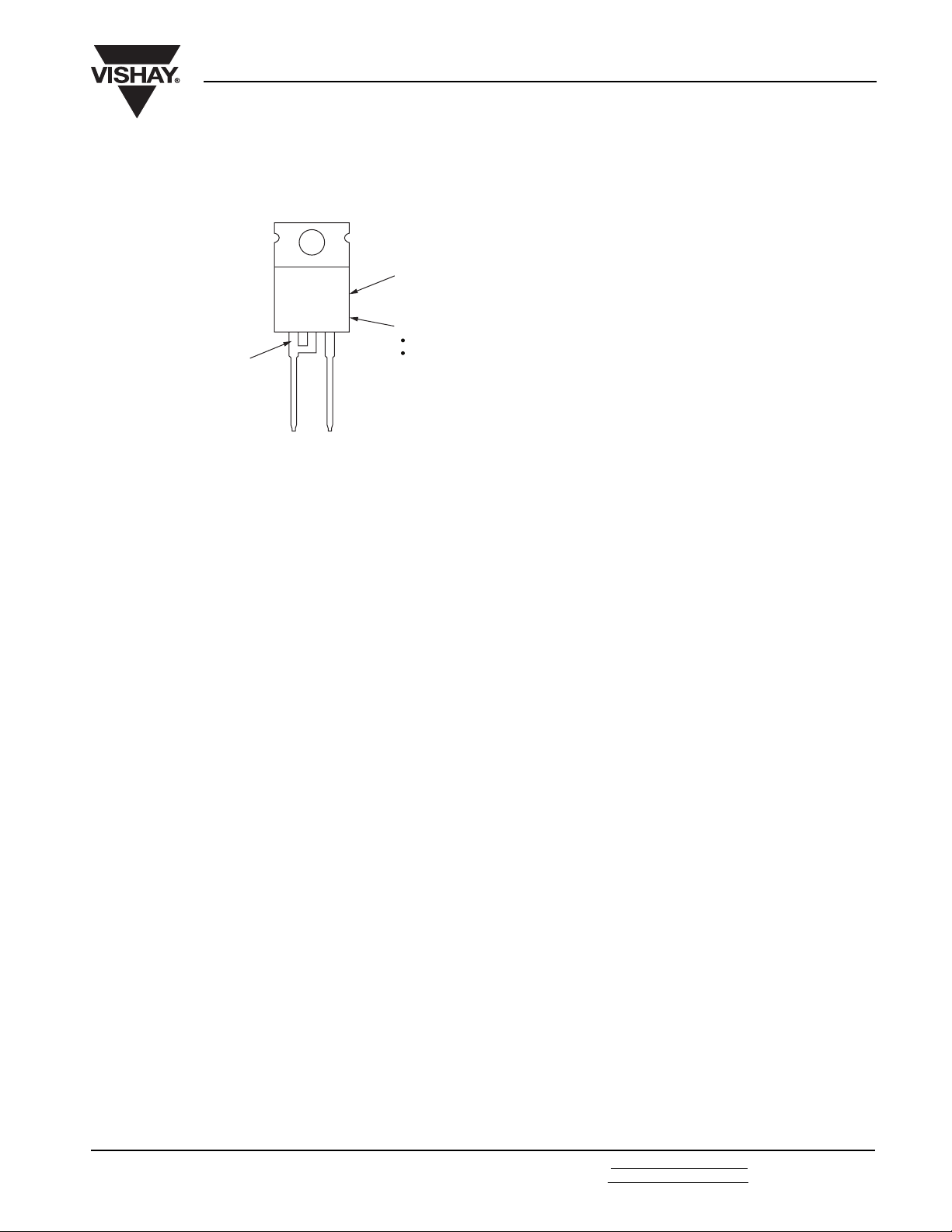
Marking device Case style TO-220AC
Note
(1)
When mounted on 1" square (650 mm2) PCB of FR-4 or G-10 material 4 oz. (140 μm) copper 40 °C/W
For recommended footprint and soldering techniques refer to application note #AN-994
- 40 to 150 °C
240 °C
2g
0.07 oz.
10ETS08
10ETS12
mA
°C/W
www.vishay.com For technical questions within your region, please contact one of the following: Document Number: 94337
2 DiodesAmericas@vishay.com
, DiodesAsia@vishay.com, DiodesEurope@vishay.com Revision: 22-Jul-10
90
150
140
130
120
110
100
4268
16
18
10 12 14
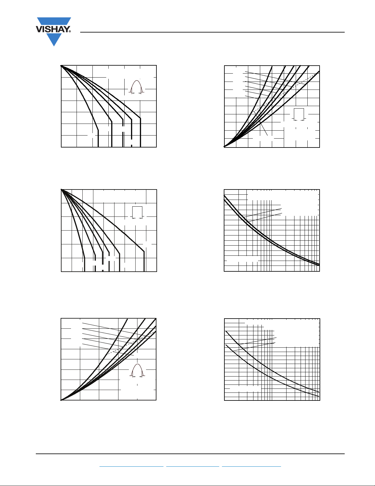
0
Maximum Allowable
Case Temperature (°C)
Average Forward Current (A)
DC
30°
60°
90°
120°
180°
10ETS.. Series
R
thJC
(DC) = 2.5 °C/W
Ø
Conduction period
10ETS08PbF, 10ETS12PbF High Voltage Series
150
140
130
120
110
100
Maximum Allowable
Case Temperature (°C)
90
80
0
2
Average Forward Current (A)
Fig. 1 - Current Rating Characteristics
Fig. 2 - Current Rating Characteristics
10ETS.. Series
R
(DC) = 2.5 °C/W
thJC
Conduction angle
60°
90°
30°
120°
468
Input Rectifier Diode, 10 A
Ø
180°
10
12
Vishay Semiconductors
20
18
16
14
12
10
Maximum Average
Forward Power Loss (W)
200
180
160
140
120
100
80
Forward Current (A)
Peak Half Sine Wave
60
40
DC
180°
120°
90°
60°
30°
8
6
4
2
0
02468
RMS limit
Conduction period
10ETS.. Series
T
J
Average Forward Current (A)
Fig. 4 - Forward Power Loss Characteristics
10ETS.. Series
1
At any rated load condition and with
rated V
applied following surge.
RRM
Initial TJ = 150 °C
at 60 Hz 0.0083 s
at 50 Hz 0.0100 s
10
Number of Equal Amplitude
Half Cycle Current Pulses (N)
Fig. 5 - Maximum Non-Repetitive Surge Current
Ø
= 150 °C
16141210
100
Maximum Average
Forward Power Loss (W)
Document Number: 94337 For technical questions within your region, please contact one of the following: www.vishay.com
Revision: 22-Jul-10 DiodesAmericas@vishay.com
16
14
12
10
180°
120°
90°
60°
30°
8
6
4
2
0
0
Fig. 3 - Forward Power Loss Characteristics
2468
Average Forward Current (A)
RMS limit
Ø
Conduction angle
10ETS.. Series
= 150 °C
T
J
240
220
200
180
160
140
120
100
Forward Current (A)
Peak Half Sine Wave
80
60
10
40
Maximum non-repetitive surge current
versus pulse train duration.
Initial T
No voltage reapplied
Rated V
10ETS.. Series
0.1 1.00.01
J
RRM
= 150 °C
reapplied
Pulse Train Duration (s)
Fig. 6 - Maximum Non-Repetitve Surge Current
, DiodesAsia@vishay.com, DiodesEurope@vishay.com 3

0.1
1
10
0.0001 0.001 0.01 0.1 1
Square Wave Pulse Duration (s)
Z
thJC
- Transient
Thermal Impedance (°C/W)
10
D = 0.50
D = 0.33
D = 0.25
D = 0.17
D = 0.08
Steady state value
(DC operation)
10ETS.. Series
Single pulse
10ETS08PbF, 10ETS12PbF High Voltage Series
Vishay Semiconductors
Input Rectifier Diode, 10 A
100
TJ = 25 °C
10
10ETS.. Series
Instantaneous Forward Current (A)
1
0.5 1.0 1.5 2.0 2.5
0
Instantaneous Forward Voltage (V)
Fig. 7 - Forward Voltage Drop Characteristics
TJ = 150 °C
3.0
Fig. 8 - Thermal Impedance Z
www.vishay.com For technical questions within your region, please contact one of the following: Document Number: 94337
4 DiodesAmericas@vishay.com
, DiodesAsia@vishay.com, DiodesEurope@vishay.com Revision: 22-Jul-10
Characteristics
thJC

1 - Current rating (10 = 10 A)
2 - Circuit configuration:
3 - Package:
4 - Type of silicon:
5 - Voltage code x 100 = V
RRM
6 - None = Standard production
PbF = Lead (Pb)-free
E = Single diode
T = TO-220AC
S = Standard recovery rectifier
08 = 800 V
12 = 1200 V
Device code
51 32 4 6
10 E T S 12 PbF
10ETS08PbF, 10ETS12PbF High Voltage Series
ORDERING INFORMATION TABLE
Input Rectifier Diode, 10 A
Vishay Semiconductors
LINKS TO RELATED DOCUMENTS
Dimensions www.vishay.com/doc?95221
Part marking information www.vishay.com/doc?95224
Document Number: 94337 For technical questions within your region, please contact one of the following: www.vishay.com
Revision: 22-Jul-10 DiodesAmericas@vishay.com
, DiodesAsia@vishay.com, DiodesEurope@vishay.com 5
Assembly
lot code
xxxxxx
V P119X
AC
TO-220AC
Part number
Product version (optional):
P = Lead (Pb)-free
None = Standard
Date code:
Year 1 = 2001
Week 19
Line X
Part Marking Information
Vishay High Power Products
Example: This is a xxxxxx with
assembly lot code AC,
assembled on WW 19, 2001
in the assembly line “X”
Document Number: 95224 For technical questions concerning discrete products, contact: diodes-tech@vishay.com
Revision: 30-Oct-08 For technical questions concerning module products, contact: ind-modules@vishay.com
www.vishay.com
1

DIMENSIONS in millimeters and inches
Outline Dimensions
Vishay High Power Products
TO-220AC
D
L3
D1
L4
Plating
A
Base metal
c1 (4)
B
Seating plane
A1
A2
View A - A
CC
E
Thermal pad
D2 (6)
E1 (6)
D
D
L1
A
H1
θ
A
123
3
DD
A
Ø P
Detail B
L1
L
MM
0.015 AB
b, b2
(6) H1
(2)
C
C
(6)
E
Q
21
CC
e1
c
SYMBOL
b1, b3
Section C - C and D - D
MILLIMETERS INCHES
MIN. MAX. MIN. MAX. MIN. MAX. MIN. MAX.
(4)
NOTES SYMBOL
2 x b2 2 x b
Detail B
MILLIMETERS INCHES
NOTES
A 3.56 4.82 0.140 0.190 E 9.66 10.66 0.380 0.420 3, 6
A1 0.51 1.40 0.020 0.055 E1 8.38 8.89 0.330 0.350 6
A2 2.04 2.92 0.080 0.115 e 2.54 BSC 0.100 BSC
b 0.38 1.01 0.015 0.040 e1 5.08 BSC 0.200 BSC
b1 0.38 0.96 0.015 0.038 4 H1 5.85 6.86 0.230 0.270 6
b2 1.15 1.77 0.045 0.070 L 12.70 14.73 0.500 0.580
b3 1.15 1.73 0.045 0.068 4 L1 3.55 3.96 0.140 0.150 2
c 0.36 0.61 0.014 0.024 L3 1.78 2.13 0.070 0.084
c1 0.36 0.56 0.014 0.022 4 L4 0.76 1.27 0.030 0.050
D 14.22 15.87 0.560 0.625 3 Ø P 3.54 3.73 0.139 0.147
D1 8.38 9.02 0.330 0.355 Q 2.54 3.05 0.100 0.120
D2 12.19 12.88 0.480 0.507 6 θ 90° to 93° 90° to 93°
Notes
(1)
Dimensioning and tolerancing per ASME Y14.5M-1994
(2)
Lead dimension and finish uncontrolled in L1
(3)
Dimension D and E do not include mold flash. Mold flash shall not exceed 0.127 mm (0.005") per side. These dimensions are measured at
the outermost extremes of the plastic body
(4)
Dimension b1, b3 and c1 apply to base metal only
(5)
Controlling dimensions: inches
(6)
Thermal pad contour optional within dimensions E, H1, D2 and E1
(7)
Outline conforms are derived from the actual package outline
Document Number: 95221 For technical questions concerning discrete products, contact: diodestech@vishay.com
www.vishay.com
Revision: 16-Nov-09 For technical questions concerning module products, contact: indmodules@vishay.com
1

Legal Disclaimer Notice
Vishay
Disclaimer
All product specifications and data are subject to change without notice.
Vishay Intertechnology, Inc., its affiliates, agents, and employees, and all persons acting on its or their behalf
(collectively, “Vishay”), disclaim any and all liability for any errors, inaccuracies or incompleteness contained herein
or in any other disclosure relating to any product.
Vishay disclaims any and all liability arising out of the use or application of any product described herein or of any
information provided herein to the maximum extent permitted by law. The product specifications do not expand or
otherwise modify Vishay’s terms and conditions of purchase, including but not limited to the warranty expressed
therein, which apply to these products.
No license, express or implied, by estoppel or otherwise, to any intellectual property rights is granted by this
document or by any conduct of Vishay.
The products shown herein are not designed for use in medical, life-saving, or life-sustaining applications unless
otherwise expressly indicated. Customers using or selling Vishay products not expressly indicated for use in such
applications do so entirely at their own risk and agree to fully indemnify Vishay for any damages arising or resulting
from such use or sale. Please contact authorized Vishay personnel to obtain written terms and conditions regarding
products designed for such applications.
Product names and markings noted herein may be trademarks of their respective owners.
Document Number: 91000 www.vishay.com
Revision: 18-Jul-08 1
 Loading...