

ViewSonic VE510s-4, ViewSonic VE510b-4 Service Manual

15” Color TFT LCD Display
Service Manual
ViewSonic VE510s-4
ViewSonic
381 Brea Canyon Road, Walnut, California 91789 USA - (800) 888-8583
(VE510s-4_VE510b-4_SM Rev. 1a Dec. 2005)
VE510b-4
VLCDS27996-3W
Model No. VLCDS27996-2W
Copyright
Copyright
¤
2005 by ViewSonic Corporation. All rights reserved. No part of this publication may be
reproduced, transmitted, transcribed, stored in a retrieval system, or translated into any language or
computer language, in any form or by any means, electronic, mechanical, magnetic, optical, chemical,
manual or otherwise, without the prior written permission of ViewSonic Corporation.
Disclaimer
ViewSonic makes no representations or warranties, either expressed or implied, with respect to the
contents hereof and specifically disclaims any warranty of merchantability or fitness for any particular
purpose. Further, ViewSonic reserves the right to revise this publication and to make changes from time
to time in the contents hereof without obligation of ViewSonic to notify any person of such revision or
changes.
Trademarks
ViewSonic is a registered trademark of ViewSonic Corporation.
All other trademarks used within this document are the property of their respective owners.
Optiquest is a registered trademark of ViewSonic Corporation.
Revision History
ECR Number
Description of Changes
EditorRevision SM Editing Date
Jamie Chang
12/02/05
1a
Initial Release
i
ViewSonic Corporation Confidential
-
Do Not Copy VE510s-4_VE510b-4
TABLE OF CONTENTS
1. Precautions and Safety Notices
2. Specification
3. Front Panel Function Control Description
4. Circuit Description
5. Adjusting Procedure
6. Trouble Shooting Flow Chart
7. Recommended Spare Parts List
8. Exploded View And Exploded Parts List
9. Block Diagram
10. Schematic Diagrams
11. PCB Layout Diagrams
ii
ViewSonic Corporation Confidential
-
Do Not Copy VE510s-4_VE510b-4
1
4
8
15
21
41
43
56
59
60
67

1. Precautions and Safety Notices (VE510s-4/VE510b-4)
1.1. SAFETY PRECAUTIONS
This monitor is manufactured and tested on a ground principle that a user's safety comes first.
However, improper use or installation may cause damage to the monitor as well as to the
user. Carefully go over the following WARNINGS before installing and keep this guide
handy.
WARNINGS:
This monitor should be operated only at the correct power sources indicated on the
label on the rear end of the monitor. If you're unsure of the power supply in your
residence, consult your local dealer or power company.
Use only the special power adapter that comes with this monitor for power input.
Do not try to repair the monitor your self as it contains no user-serviceable parts. This
monitor should only be repaired by a qualified technician.
Do not remove the monitor cabinet. There is high-voltage parts inside that may cause
electric shock to human bodies, even when the power cord is unplugged.
Stop using the monitor if the cabinet is damaged. Have it checked by a service
technacian.
Put your monitor only in a clean, dry environment. If it gets wet, unplug the power
cable immediately and consult your service technician.
Always unplug the monitor before cleaning it. Clean the cabinet with a clean, dry cloth.
Apply non-ammonia based cleaner onto the cloth, not directly onto the glass screen.
Keep the monitor away from magnetic objects, motors, TV sets, and transformer.
Do not place heavy objects on the monitor or power cord.
1.2. PRODUCT SAFETY NOTICE
Many electrical and mechanical parts in this chassis have special safety visual inspections
and the protection afforded by them cannot necessarily be obtained by using replacement
components rated for higher voltages, wattage, etc. Before replacing any of these
components read the parts list in this manual carefully. The use of substitute replacement
parts which do not have the same safety characteristics as specified in the parts list may
create shock, fire, or other hazards.
1.3. SERVICE NOTES
1. When replacing parts or circuit boards, clamp the lead wires around terminals before
soldering.
2. When replacing a high wattage resistor (more than 1W of metal oxide film resistor) in
circuit board, keep the resistor about 5mm away from circuit board.
3. Keep wires away from high voltage, high temperature components and sharp edges.
4. Keep wires in their original position so as to reduce interference.
5. Usage of this product please refer to also user's manual.
1
ViewSonic Corporation Confidential
-
Do Not Copy VE510s-4_VE510b-4
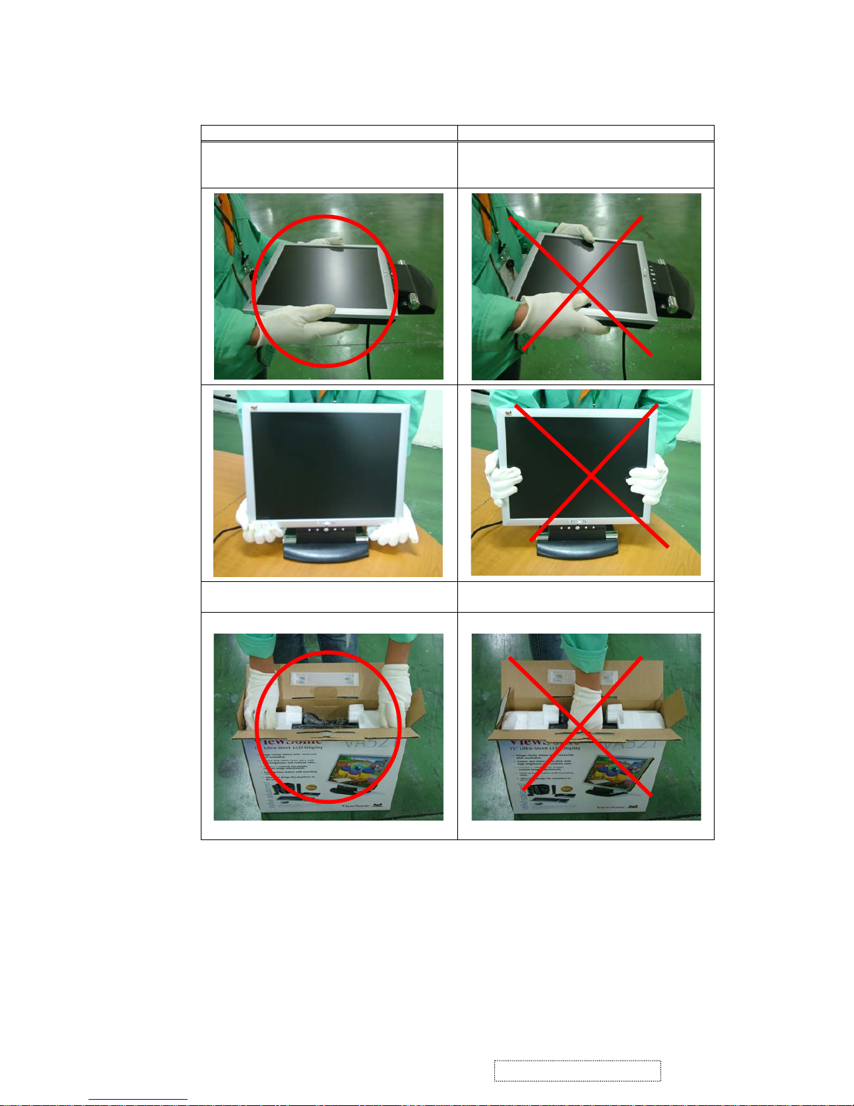
1.4. HANDLING AND PLACING METHODS
Correct Methods: Incorrect Methods:
Only touch the metal frame of the LCD panel
or the front cover of the monitor. Do not touch
the surface of the polarizer.
Surface of the LCD panel is pressed by fingers
and that may cause “Mura”
Take out the monitor with cushions Taking out the monitor by grasping the LCD
panel. That may cause “Mura”
2
ViewSonic Corporation Confidential
-
Do Not Copy VE510s-4_VE510b-4

Place the monitor on a clean and soft foam pad. Placing the monitor on foreign objects. That
could scratch the surface of the panel or cause
“Mura”
The panel is placed facedown on the lap. That
may cause “Mura”
3
ViewSonic Corporation Confidential
-
Do Not Copy VE510s-4_VE510b-4

2. Specification
2.1. PRODUCT SPECIFICATION
LCD Panel 15.0" TFT
Power Management Energy Star compliant VESA
DPMS compatible
< 1W
Displayable Resolution XGA 1024× 768 (max.)
Pixel Dimension 0.297× 0.297mm
LCD Display Color 16.2M Color Max. (8bit)
Viewing Angle CR≥10
Horizontal: 130°
Vertical: 100°
TILT -5°~ -25°
Contrast Ratio 400: 1 (min.)
500: 1 (typ.)
Brightness 200 cd/m2 (min.)
250 cd/m2 (typ.)
Response Time Tr + Tf : 16ms (typ.)
Active Display Area 304.1mm× 228.1mm
Temperature Operating: 0°C ~ +35°C
Storage: -20°C ~ +60°C
Power Input Voltage: 100~240 Vac
Consumption: 30 Watts (Max.)
4
ViewSonic Corporation Confidential
-
Do Not Copy VE510s-4_VE510b-4
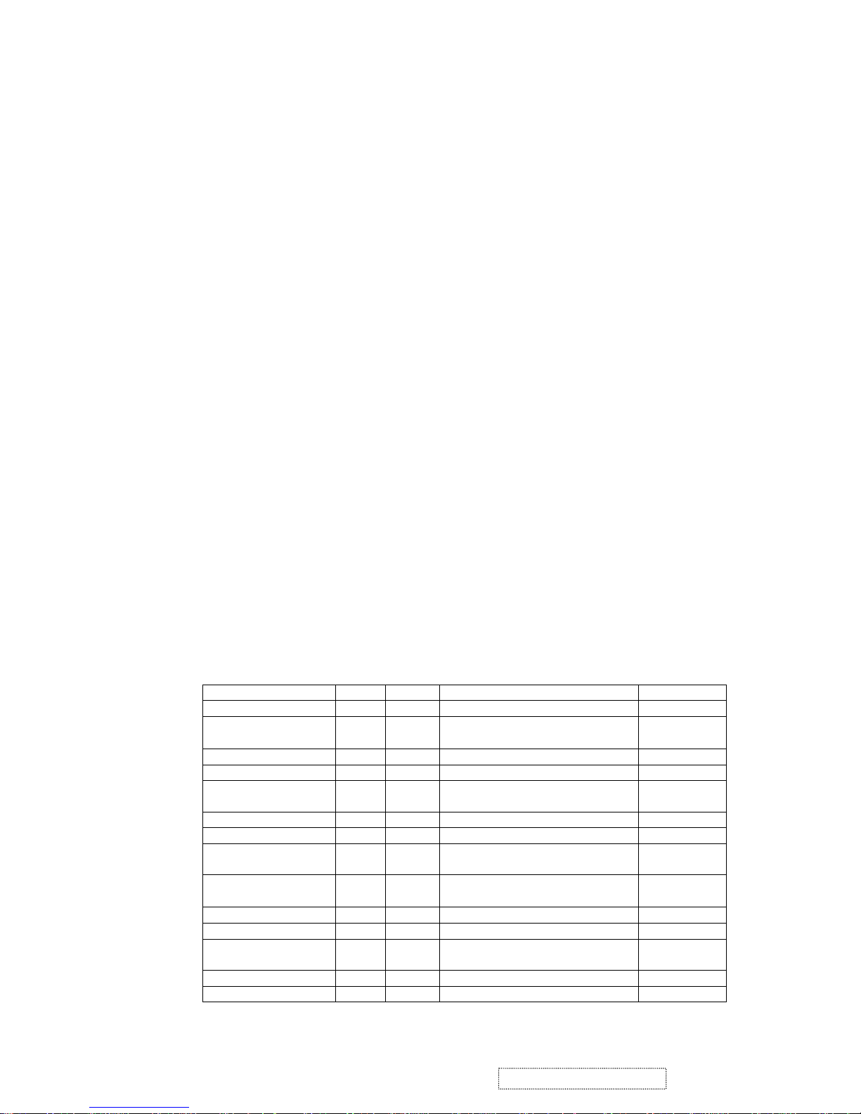
2.2. SUPPORTING TIMING CHART
ITEM 1 2 3 4 5
TIMING
640×350@70Hz 640×480@60Hz 640×480@67Hz 640×480@75Hz 640×480@72Hz
Pixel Rate 25.175MHz 25.175MHz 30.240MHz 31.500MHz 31.500MHz
H TOTAL 31.778us 31.778us 28.571us 26.667us 26.413us
H DISPLAY 25.422us 25.422us 21.164us 20.317us 20.317us
H B-Porch 1.907us 1.907us 3.175us 3.810us 4.063us
H Width 3.813us 3.813us 2.116us 2.032us 0.270us
H Border 0.318us 0.318us 0.000us 0.000us 0.000us
V TOTAL 14.268ms 16.683ms 15.000ms 13.334ms 13.734ms
V DISPLAY 11.122ms 15.253ms 13.714ms 12.800ms 12.678ms
V B-Porch 1.907ms 1.049ms 1.114ms 0.427ms 0.528ms
Vs Width 0.064ms 0.064ms 0.086ms 0.080ms 0.079ms
V Border 0.191ms 0.254ms 0.000ms 0.000ms 0.000ms
H/V Sync +/- -/- -/- -/- -/-
Interlace No. No. No. No. No.
ITEM 6 7 8 9 10
TIMING
640×480@85Hz 720×400@70Hz 800×600@56Hz 800×600@60Hz 800×600@72Hz
Pixel Rate 36.000MHz 28.322MHz 36.000MHz 40.000MHz 50.000MHz
H TOTAL 22.111us 31.778us 28.444us 26.400us 20.800us
H DISPLAY 17.778us 25.422us 22.222us 20.000us 16.000us
H B-Porch 2.222us 1.907us 3.556us 2.200us 1.280us
H Width 1.556us 3.813us 2.000us 3.200us 2.400us
H Border 0.000us 0.318us 0.000us 0.000us 0.000us
V TOTAL 11.764ms 14.268ms 17.778ms 16.579ms 13.853ms
V DISPLAY 11.093ms 12.711ms 17.066ms 15.840ms 12.480ms
V B-Porch 0.578ms 1.112ms 0.626ms 0.607ms 0.478ms
Vs Width 0.069ms 0.064ms 0.057ms 0.106ms 0.125ms
V Border 0.000ms 0.222ms 0.000ms 0.000ms 0.000ms
H/V Sync -/- -/+ +/+ +/+ +/+
Interlace No. No. No. No. No.
5
ViewSonic Corporation Confidential
-
Do Not Copy VE510s-4_VE510b-4
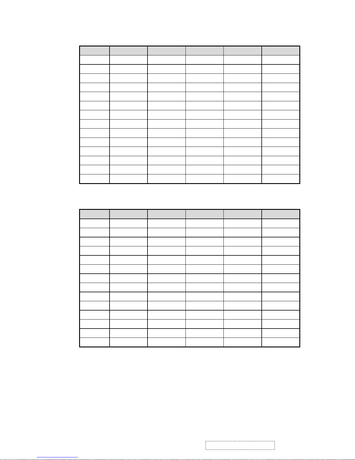
ITEM 11 12 13 14 15
TIMING
800×600@75Hz 800×600@85Hz 832×624@74.5Hz 1024×768@60Hz 1024×768@70Hz
Pixel Rate 48.500MHz 56.250MHz 57.280MHz 65.000MHz 75.000MHz
H TOTAL 21.333us 18.631us 20.112us 20.677us 17.707us
H DISPLAY 16.162us 14.222us 14.525us 15.754us 13.653us
H B-Porch 3.232us 2.702us 3.771us 2.462us 1.920us
H Width 1.616us 1.138us 1.118us 2.092us 1.813us
H Border 0.000us 0.000us 0.000us 0.000us 0.000us
V TOTAL 13.333ms 11.756ms 13.417ms 16.666ms 14.272ms
V DISPLAY 12.800ms 11.179ms 12.552ms 15.880ms 13.599ms
V B-Porch 0.448ms 0.503ms 0.784ms 0.600ms 0.513ms
Vs Width 0.064ms 0.056ms 0.060ms 0.124ms 0.106ms
V Border 0.000ms 0.000ms 0.00ms 0.000ms 0.000ms
H/V Sync +/+ +/+ -/- -/- -/-
Interlace No. No. No. No. No.
ITEM 16 17
TIMING
1024×768@72Hz 1024×768@75Hz
Pixel Rate 77.066MHz 78.750MHz
H TOTAL 17.232us 16.660us
H DISPLAY 13.287us 13.003us
H B-Porch 1.869us 2.235us
H Width 1.765us 1.219us
H Border 0.000us 0.000us
V TOTAL 13.889ms 13.328ms
V DISPLAY 13.234ms 12.795ms
V B-Porch 0.500ms 0.466ms
Vs Width 0.103ms 0.050ms
V Border 0.000ms 0.000ms
H/V Sync -/- +/+
Interlace No. No.
6
ViewSonic Corporation Confidential
-
Do Not Copy VE510s-4_VE510b-4
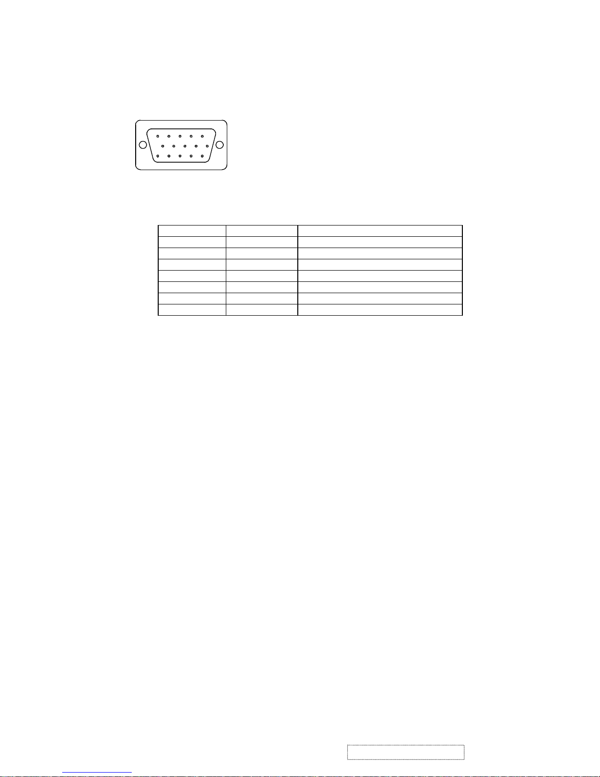
2.3. D-SUB CONNECTOR
D-SUB 15 PIN CONNECTOR
1.Red Video 6.Red GND 11.NC
2.Green Video 7.Green GND 12.SDA
3.Blue Video 8.Blue GND 13.H-sync
4.NC 9. +5V for DDC 14.V-sync
5.GND 10.GND 15.SCL
12345
678910
11 12 13 14 15
SIGNAL LEVEL
CONNECTOR SIGNAL DESCRIPTION
R RED 0.7vp-p(VIDEO)
G GREEN 0.7vp-p(VIDEO)
B BLUE 0.7vp-p(VIDEO)
H H/SYNC TTL positive or negative
V V/SYNC TTL positive or negative
SDA DDC1/2B TTL
SCL DDC1/2B TTL
7
ViewSonic Corporation Confidential
-
Do Not Copy VE510s-4_VE510b-4
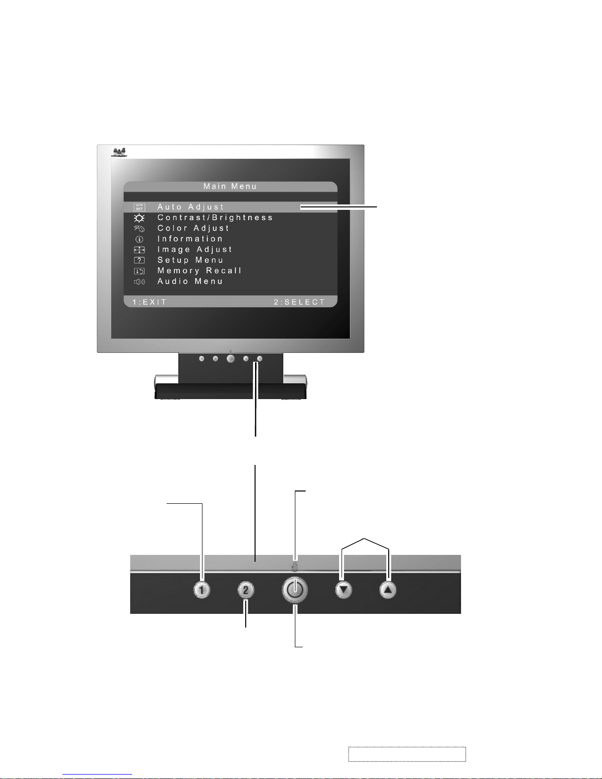
Scroll through menu
options and adjust the
displayed control.
Displays, saves
changes to, and exits
the Main Menu.
Power On/Off
Selects a highlighted control. Also,
displays the control screen for the
selected control and toggles
between control pairs.
Power light
Front Control Panel
Main Menu
with OnView controls
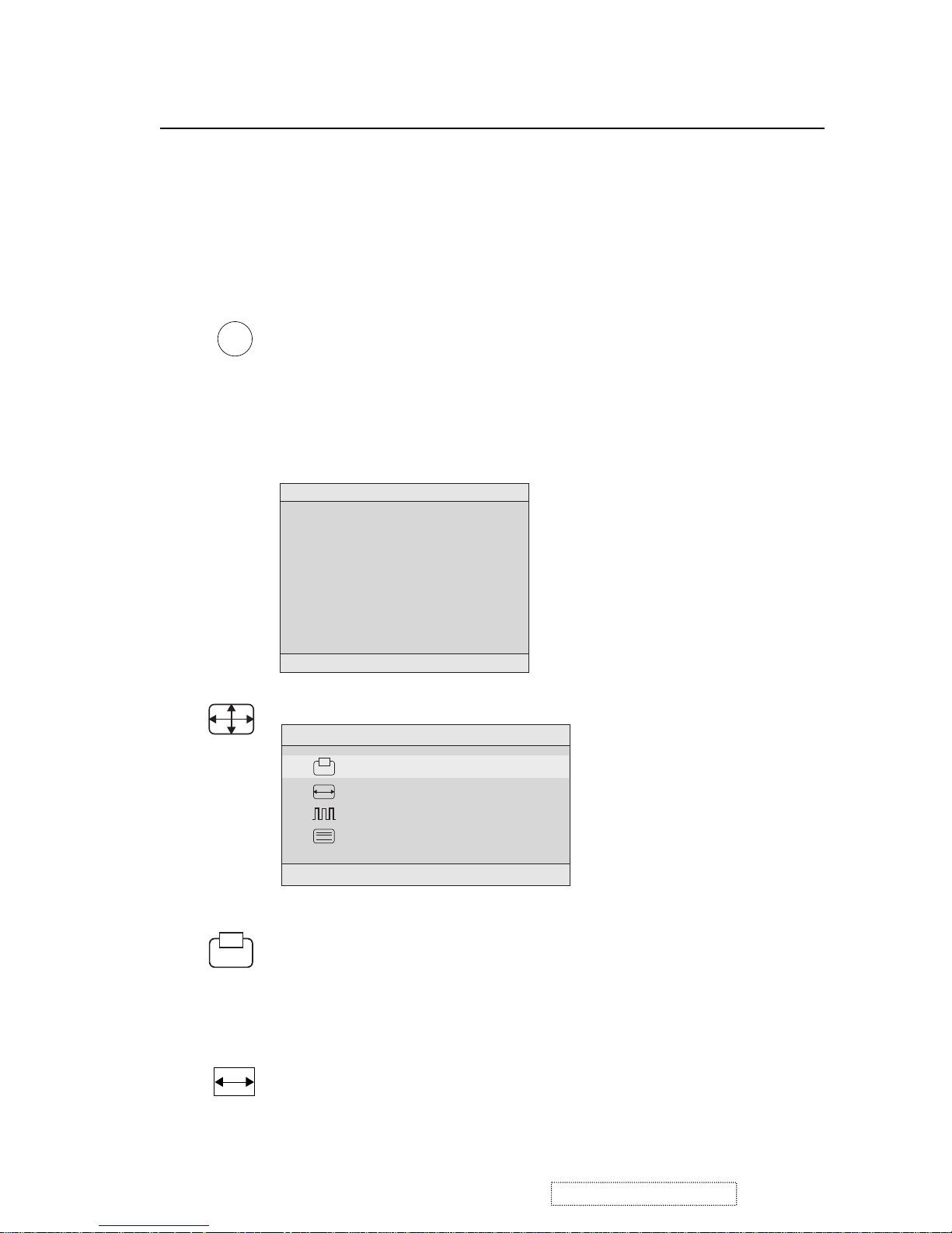
3. Front Panel Function Control Description
VE510s-4/VE510b-4
8
ViewSonic Corporation Confidential
-
Do Not Copy VE510s-4_VE510b-4
. (The black border around the
edge of the screen should barely touch the illuminated “active area” of the
LCD display.)
The line at the
bottom of the
screen tells you
what you can do
next: Exit or Select
the control that is
highlighted.
Main Menu
1:EXIT 2:SELECT
Auto Adjust
Contrast/Brightness
Color Adjust
Information
Image Adjust
Setup Menu
Memory Recall
AUTO
SET
i
?
Do the following to adjust the screen image:
1
To display the Main Menu, press button [1].
4
To adjust the control, press the up I or down J buttons.
5
To save the adjustments and exit the menu, press button [1] twice.
The following tips may help you optimize your display:
• Adjust your computer's graphic card so that it outputs a video signal 1024 x
768 @ 60 Hz to the LCD display. (Look for instructions on “changing the
refresh rate” in your graphic card's user guide.)
• If necessary, make small adjustments using H. POSITION and V. POSITION
until the screen image is completely visible
NOTE: All OnView menus and adjustment screens disappear automatically
after about 15 seconds. This time period is adjustable through the Setup
menu and the OSD timeout control described on page 11.
2
To highlight a control you want to adjust, press I or J to scroll up or down
the Main Menu.
3
To select the highlighted control, press button [2]. A control screen appears
like the example shown below.
Contrast
1:EXIT 2: Brightness
9
ViewSonic Corporation Confidential
-
Do Not Copy VE510s-4_VE510b-4
Main Menu Controls
Adjust the menu items shown below by using the up Iand down Jbuttons.
Control Explanation
Auto Adjust
automatically sizes, centers, and fine tunes the
video signal to eliminate waviness and distortion.
Press the [2] button to obtain a sharper image.
NOTE
: Auto Adjust works with most common video cards. If
this function does not work on your LCD display, then lower the
video refresh rate to 60 Hz and set the resolution to its pre-set
value.
Contrast
adjusts the difference between the image background
(black level) and the foreground (white level).
Brightness
adjusts background black level of the screen image.
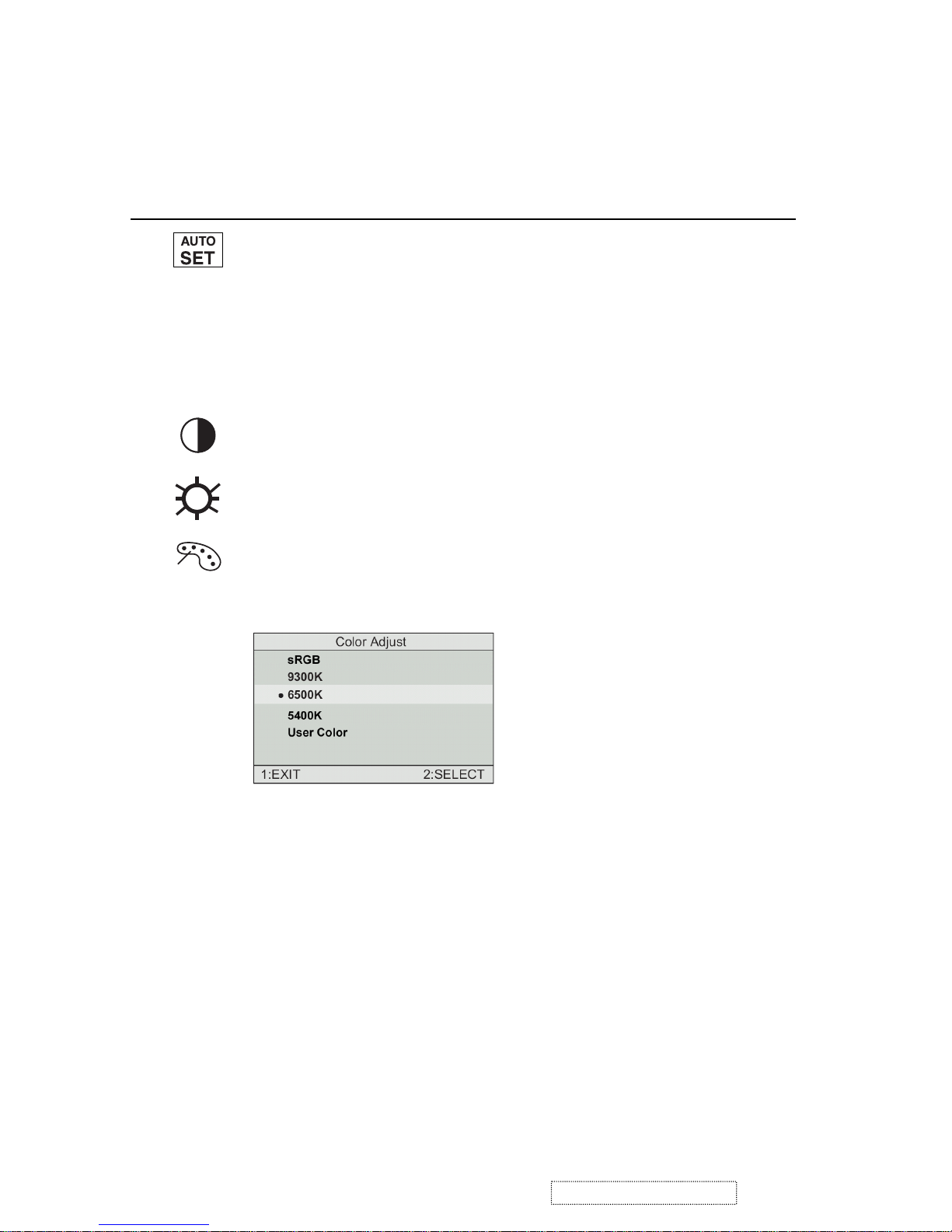
Color Adjust
provides several color options: preset color
temperatures and User which allows you to adjust red (R), green
(G), and blue (B). The factory setting for this product is 6500K
(6500 Kelvin).
9300K
— Adds blue to the screen image for cooler white (used
in most office settings with fluorescent lighting).
6500K
— Adds red to the screen image for warmer white and
richer red.
5400K
— Adds green to the screen image for a darker color.
sRGB
— sRGB is quickly becoming the industry standard for
color management, with support being included in many of the
latest applications. Enabling this setting allows the LCD display
to more accurately display colors the way they were originally
intended. Enabling the sRGB setting will cause the Contrast and
Brightness adjustments to be disabled.
10
ViewSonic Corporation Confidential
-
Do Not Copy VE510s-4_VE510b-4
Information
displays the timing mode (video signal input)
coming from the graphics card in your computer. See your
graphic card’s user guide for instructions on changing the
resolution and refresh rate (vertical frequency).
VESA 1024 x 768 @ 60 Hz (recommended) means that the
resolution is 1024 x 768 and the refresh rate is 60 Hertz.
Control Explanation
i
H. Size
(Horizontal Size) adjusts the width of the screen image.
NOTE:
Vertical size is automatic with your LCD display.
H./V. Position
adjusts horizontal and vertical position of the
screen image. You can toggle between Horizontal and Vertical
by pressing button [2]. Horizontal moves the screen image to
the left or to the right. Vertical moves the screen image up and
down.
Information
1:EXIT
H. Frequency: 48.60 KHz
V. Frequency: 60.00 Hz
Pixel Clock: 65.00 MHz
Resolution: 1024 x 768
Model Number: VLCDS23585-2W
Serial No:
www.viewsonic.com
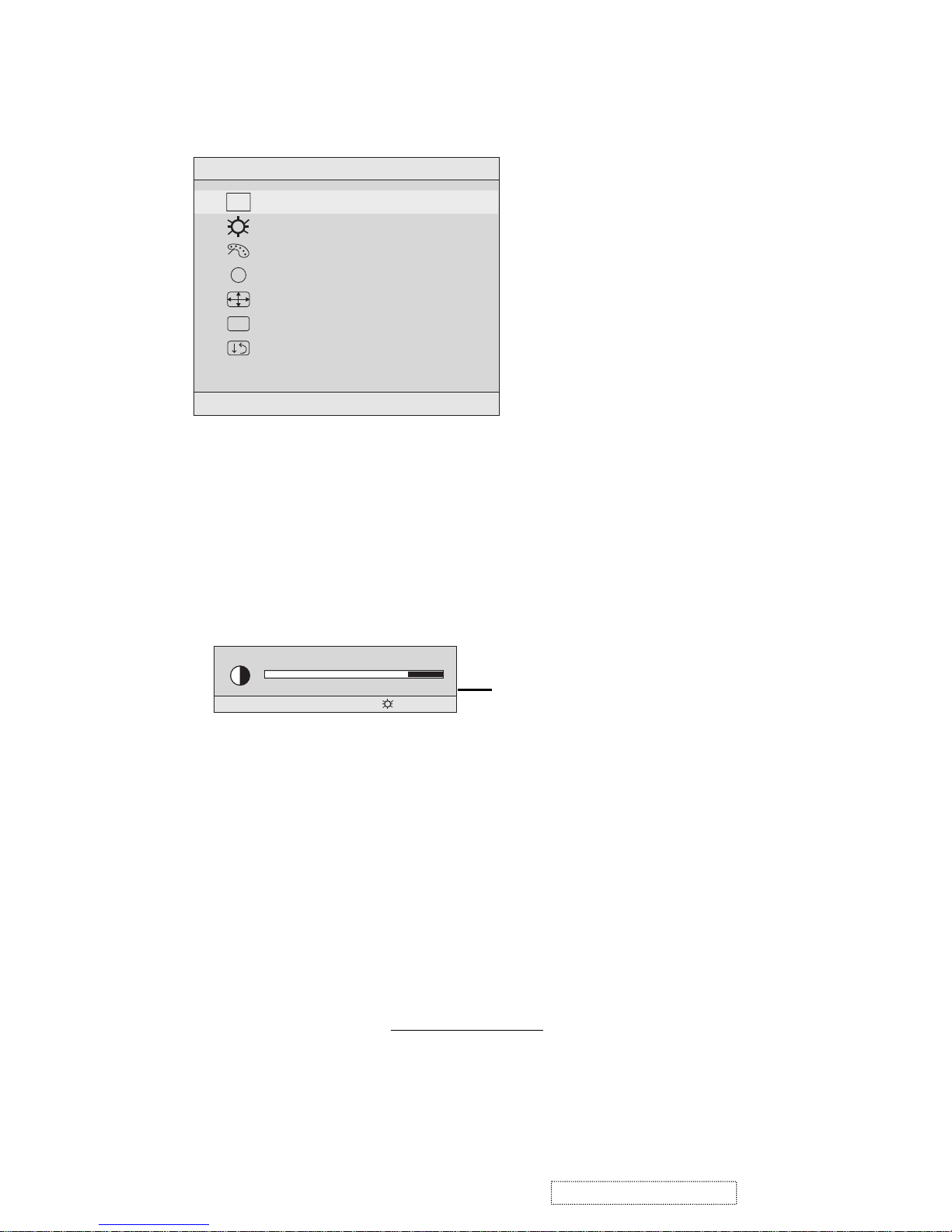
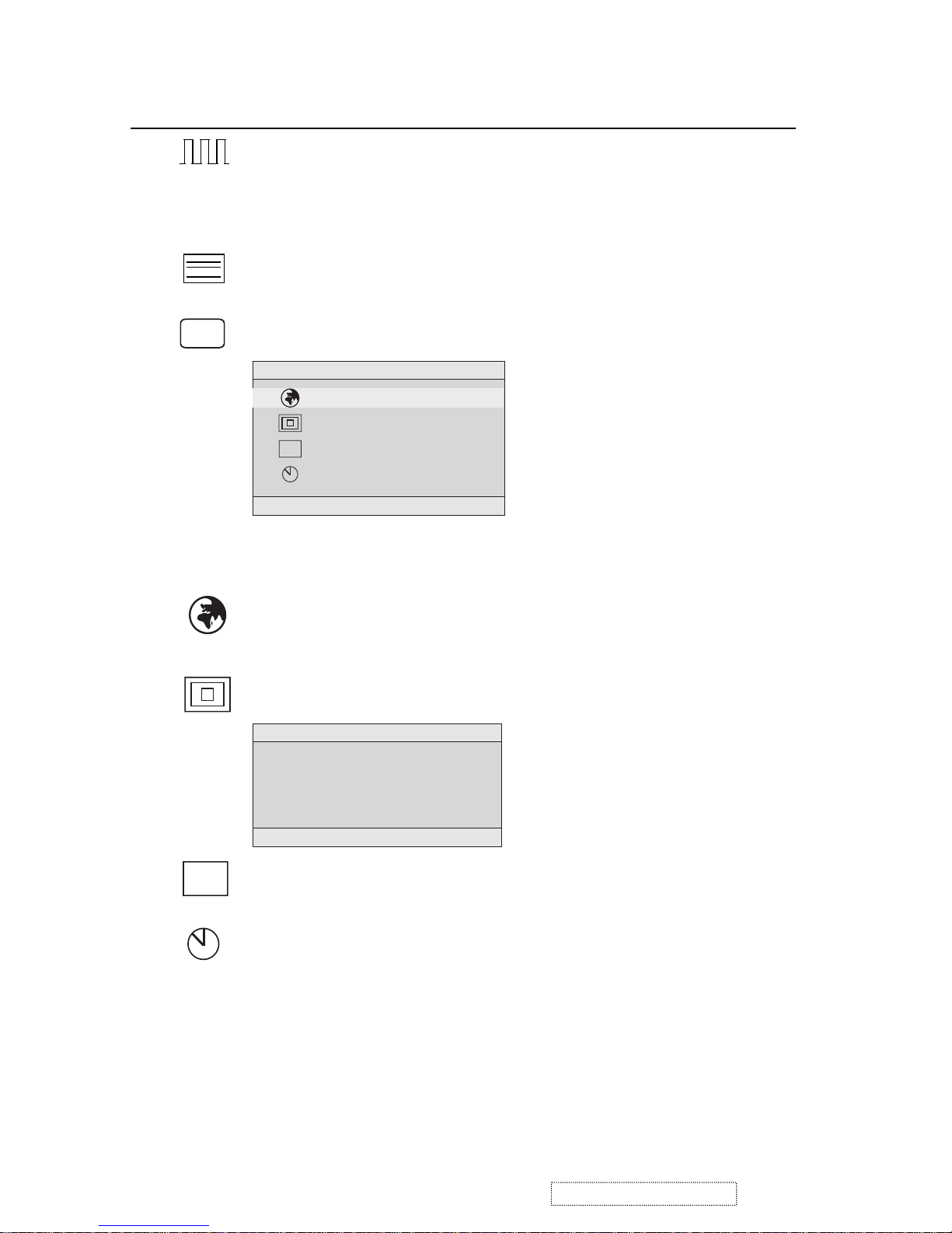
Image Adjust
The Image Adjust controls are explained below:
Image Adjust
1:EXIT 2:SELECT
H./V. Position
H. Size
Fine Tune
Sharpness
User Color
— Individual adjustments for red (R), green (G),
and blue (B)
.
1
To select color (R, G or B) press button [2].
2
To adjust selected color, press ▲ or ▼.
Important
: If you select RECALL from the Main Menu when
the product is set to a Preset Timing Mode, colors return to the
6500K factory preset.
11
ViewSonic Corporation Confidential
-
Do Not Copy VE510s-4_VE510b-4
Fine Tune sharpens focus by aligning the illuminated text and/
or graphic characters.
NOTE:TrytheAuto Adjustbefore using the Fine
Tune control.
Sharpness
adjusts the clarity and focus of the screen image.
Setup Menu displays the menu shown below.
Control Explanation
Setup Menu
1:EXIT 2:SELECT
Language Select
Resolution Notifier
OSD Position
OSD Timeout
OSD
Resolution Notice
For best picture quality
change the resolution to
1024 x 768
1:EXIT 2:DISABLE
the menus and control screens.
The Setup Menu controls are explained below.
OSD Position
allows you to move the on-screen display menus
and control screens.
OSD Timeout
sets the length of time an on-screen display
screen is displayed. For example, with a “15 second” setting, if
a control is not pushed within 15 seconds, the display screen
disappears.
Resolution Notice
advises the optimal resolution to use.
Language
Select allows you to choose the language used in
OSD
?
12
ViewSonic Corporation Confidential
-
Do Not Copy VE510s-4_VE510b-4

Memory Recall
returns adjustments to the original factory
settings if the display is operating in a factory Preset Timing
Mode listed in this user guide.
Control Explanation
13
ViewSonic Corporation Confidential
-
Do Not Copy VE510s-4_VE510b-4
Short Cut Key
Function Key : 5 Keys !!!! 1 2 ▼
▼▼▼
▲▲▲▲
[1] Main Menu
[2] Auto Image Adjust
[▼▼▼▼] or [▲▲▲▲]
to immediately activate Contrast menu.
It should be change to Brightness OSD
by push button [2].
[▼▼▼▼] + [▲▲▲▲]
recall Contrast or Brightness while in
the Contrast or Brightness adjustment,
or recall both of Contrast and
Brightness when the OSD is not open.
[1] + [2] toggle 720x400 and 640x400 mode when
input 720x400 or 640x400 mode.
[1] + [▼▼▼▼] + [▲▲▲▲]
(Keep pushing 5 sec)
White Balance.
[1] + [▼▼▼▼]
Power Lock
[1] + [▲▲▲▲]
OSD Lock
14
ViewSonic Corporation Confidential
-
Do Not Copy VE510s-4_VE510b-4
4. Circuit Description (VE510s-4/VE510b-4)
A. AC-DC CONVERTER
The power supply with a high-integrated green-mode PWM controller provides several
features to enhance the performance of power flyback converters.
I801 is a PWM controller and provides many protection functions.
I802 is a photo couple to transfer the feedback signal from the second side which I803
detected both of the output DC voltage on 3.3V and 12V.
D813 detected the working voltage on I801 and Q805 would pull down the voltage on I801
pin5 to shut down I801 if feedback loop was failed.
R826 would be a dynamic load which was active while backlight was turned off and system
still working on, this kept 12V output voltage under 13V to protect the panel. After system
went to power saving mode, the R826 would no loaded. This was detected by I804 and Q803
active the R826 to load or not.
B. Scaling controller
The RTD2013 ADC is to convert RGB analog signal to digital signal that scaling chip can
acknowledge.
The HSYNC input receives a logic signal and provides the frequency reference for pixel clock
generation.
The scaling IC is to converts the input signal ranging from VGA to XGA into XGA resolution
that panel can acknowledge.
General
Embedded dual DDC support DDC1, DDC2B,DDC/CI
Zoom scaling up and down
Embedded Pattern Generator
No external memory required.
Require only one crystal to generate all timing
Embedded reset control output
Embedded crystal output to MICROP
3 channels 8 bits PWM output, and selectable PWM clock frequency.
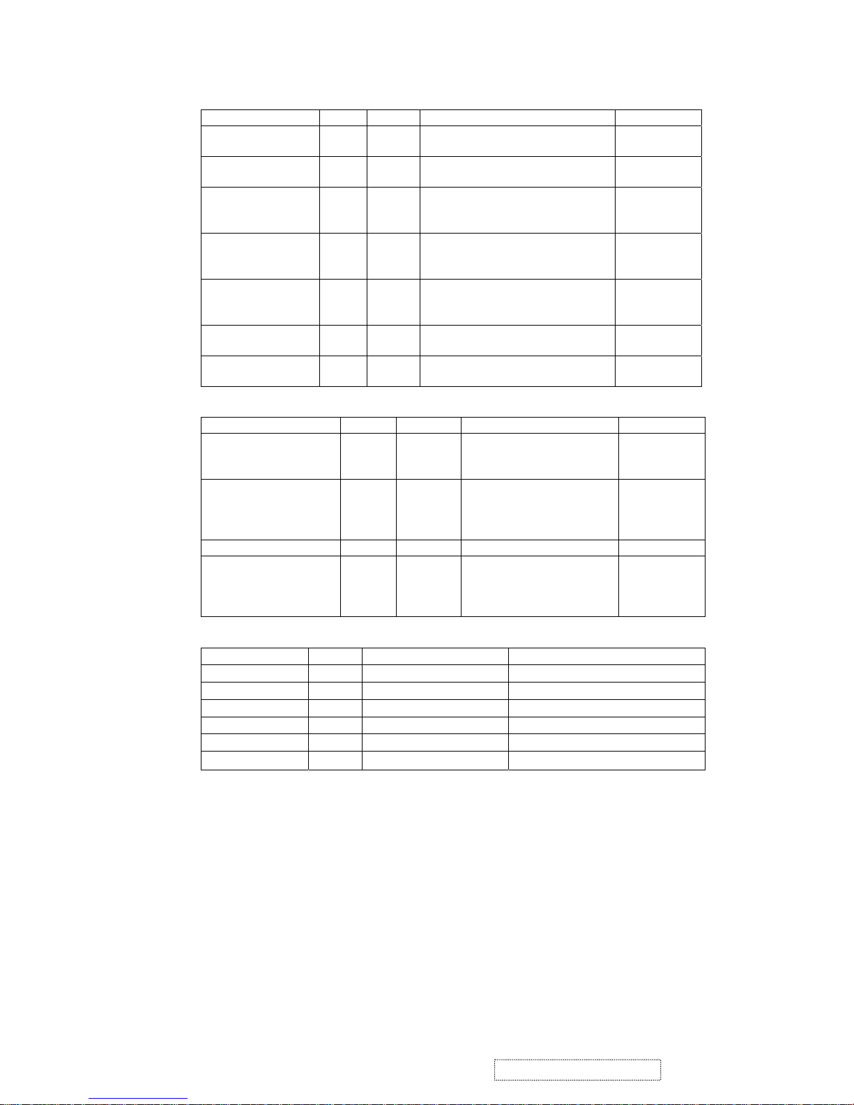
PIN DESCRIPTION
(I/O Legend: A= Analog , I=Input ,O=Output ,P=Power ,G=Ground)
■ ADC: 15 pins
Name I/O Pin No Description Note
ADC_ GND AG 27 ADC ground
ADC_REFIO AP 28 ADC band-gap voltage de-coupling 1.20V
ADC_VDD AP 29 Analog power (3.3V)
BLUE+ AI 30 Analog input from BLUE channel
BLUE- AI 31 Analog input ground from BLUE
channel
ADC_ GND AG 32 ADC ground
SOG/ADC_TEST AIO 33 SOG in/ADC test pin
GREEN+ AI 34 Analog input from GREEN channel
GREEN- AI 35 Analog input ground from GREEN
channel
ADCB_VDD AP 36 Analog power (3.3V)
RED+ AI 37 Analog input from RED channel
RED_ AI 38 Analog input ground from RED
channel
ADC_GND AG 39 Analog ground
ADC_GND AG 40 Analog ground
15
ViewSonic Corporation Confidential
-
Do Not Copy VE510s-4_VE510b-4
ADC_VDD AP 41 Analog power (3.3V)
AHS AI 42 Analog HS input (10), (4), (5)
AVS AI 43 Analog VS input (2), (4), (5)
■ PLL:8 pins
Name I/O Pin No Description Note
XO AI 1 Reference clock output
XI AO 2 Reference clock input
DPLL GND AG 3 Ground for digital PLL
DPLL VDD AP 4 Power for digital PLL (3.3V)
APLL VDD AP 5 Power for multi-phase PLL (3.3V)
PLL TEST1 AIO 6 Test Pin 1 / IRQ# 3.3V tolerance
PLL TEST2 AIO 7 Test Pin 2/Power-on-latch for crystal
out Frequency
APLL GND AG 8 Ground for multi-phase PLL
■ Control Interface: 7 pins
Name I/O Pin No Description Note
SDIO [0] IO 54 Serial control I/F data in/Parallel port
data [0]
(2), (3), / 2mA
SDIO [1] / TCON [4]
/ BBLU [0]
IO 53 Parallel port data [1] / TCON [4] /
TTL BBLU [0]
(1), (2), (3), /
2mA
SDIO [2] / TCON [3]
/ BBLU [1]
IO 52 Parallel port data [1] / TCON [3] /
TTL BBLU [1]
(1), (2), (3), /
2mA
SDIO [3] / PWM2 /
TCON [2]
IO 51 Parallel port data [1] / TCON [4] /
PWM2
(1), (2), (3), /
2mA
SCLK I 50 Serial control I/F clock (2), (3), (5)
SCSB I 111 Serial control I/F chip select (2), (3), (5)
RESET O 56 RESET output for Micron (2), (5), (6) /
2mA
■ Display & TCON/VIDEO-8 Port: 54 pins
:LVDS+RSDS+TTLO :RSDS+TTLO :RSDS+TTLIO :TTLO :TTL
IO
Pin
NO
6-bits Dual
RSDS
6-bits
Single
RSDS
8/6 bits
Dual/Single
LVDS
8 bits
Dual/Single
TTL
6 bits Dual
TTL
6 bits
Single TTL
Note
51 S [3] /
TCON [2] /
PWM2
S 3] /
TCON [2] /
PWM2
S [3] /
TCON [2] /
PWM2
S [3] /
TCON [2] /
PWM2
S [3] /
TCON [2] /
PWM2
S [3] /
TCON [2] /
PWM2
(1), (2), (3),
/ 2mA
52 S [2] /
TCON [3]
S [2] /
TCON [3]
S [2] /
TCON [3]
S [2] /
BBLU [1] /
TCON [3]
S [2] /
TCON [3]
S [2] /
TCON [3]
(1), (2), (3),
/ 2mA
53 S [1] /
TCON [4]
S [1] /
TCON [4]
S [1] /
TCON [4]
S [1] /
BBLU [0] /
TCON [4]
S [1] /
TCON [4]
S [1] /
TCON [4]
(1), (2), (3),
/ 2mA
55 PWM2 /
COUT /
TCON [13]
PWM2 /
COUT /
TCON [13]
PWM2 /
COUT /
TCON [13]
PWM2 /
COUT /
TCON [13]
PWM2 /
COUT /
TCON [13]
PWM2 /
COUT /
TCON [13]
(1), (2), (3),
/ 2mA
59 BB3P BB3P NC BBLU [7] BBLU [7] BBLU [7]
60 BB3N BB3N NC BBLU [6] BBLU [6] BBLU [6]
61 BB2P BB2P NC BBLU [5] BBLU [5] BBLU [5]
62 BB2N BB2N NC BBLU [4] BBLU [4] BBLU [4]
63 BB1P BB1P NC BBLU [3]
/T0
BBLU [3] BBLU [3]
64 BB1N BB1N NC BBLU [2]
/T1
BBLU [2] BBLU [2]
16
ViewSonic Corporation Confidential
-
Do Not Copy VE510s-4_VE510b-4
65 BCLKP BCLKP NC BGRN [1] /
T2
TCON [6] TCON [6]
66 BCLKN BCLKN NC BGRN [0] /
T3
TCON [5] TCON [5]
67 BG3P BG3P NC BGRN [7] BGRN [7] BGRN [7]
68 BG3N BG3N NC BGRN [6] BGRN [6] BGRN [6]
73 BG2P BG2P TODP
BGRN [5] /
T4
BGRN [5] BGRN [5]
74 BG2N BG2N TODN
BGRN [4] /
T5
BGRN [4] BGRN [4]
75 BG1P BG1P TOCLKP
BGRN [3] /
T6
BGRN [3] BGRN [3]
76 BG1N BG1N TOCLKN
BGRN [2] /
T7
BGRN [2] BGRN [2]
77 BR3P BR3P TOCP
BRED [7] /
T8
BRED [7] BRED [7]
78 BR3N BR3N TOCN
BRED [6] /
T9
BRED [6] BRED [6]
79 BR2P BR2P TOBP
BRED [5] /
T10
BRED [5] BRED [5]
80 BR2N BR2N TOBP
BRED [4] /
T11
BRED [4] BRED [4]
81 BR1P BR1P TOAP
BRED [3] /
T12
BRED [3] BRED [3]
82 BR1N BR1N TOAP
BRED [2] /
T13
BRED [2] BRED [2]
85 AB3P NC TEDP
ABLU [7] /
T14
ABLU [7] ABLU [7]
86 AB3N NC TEDN
ABLU [6] /
T15
ABLU [6] ABLU [6]
87 AB2P NC TECLKP
ABLU [5] /
T16
ABLU [5]
ABLU [5]
88 AB2N
NC
TECLKN
ABLU [4] /
T17
ABLU [4] ABLU [4]
89 AB1P
NC
TECP
ABLU [3] /
T18
ABLU [3] ABLU [3]
90 BB1N
NC
TECN
ABLU [2] /
T19
ABLU [2] ABLU [2]
91 ACLKP
NC
TEBP
ABLU [1] /
T20
TCON [1] TCON [1]
92 ACLKN
NC
TEBN
ABLU [0] /
T21
TCON [0] TCON [0]
93 AG3P
NC
TEAP
AGRN [7] /
T22
AGRN [7] AGRN [7]
94
AG3N NC
TEAN
AGRN [6] /
T23
AGRN [6] AGRN [6]
99
AG2P
TCON [11]
NC AGRN [5] /
T24
AGRN [5] AGRN [5]
100
AG2N TCON [10] NC AGRN [4] /
T25
AGRN [4] AGRN [4]
101
AG1P TCON [9] NC AGRN [3] /
T26
AGRN [3] AGRN [3]
102
AG1N TCON [8] NC AGRN [2] /
T27
AGRN [2] AGRN [2]
103 AR3P
TCON [7] NC
ARED [7] /
T28
ARED [7] ARED [7]
104 AR3N
TCON [6] NC ARED [6] /
T29
ARED [6] ARED [6]
17
ViewSonic Corporation Confidential
-
Do Not Copy VE510s-4_VE510b-4
105 AR2P
TCON [5] NC ARED [5] /
TH
ARED [5] ARED [5]
106 AR2N
TCON [1] NC ARED [4] /
TV
ARED [4] ARED [4]
107 AR1P
TCON [0] NC ARED [3] /
TE
ARED [3] ARED [3]
108 AR1N NC
NC ARED [2] /
TK
ARED [2] ARED [2]
113 PWM2 /
COUT /
TCON [12]
PWM2 /
COUT /
TCON [12]
PWM2 /
COUT /
TCON [12]
ARED [1] COUT PWM2 /
COUT /
TCON [12]
(9)
114 TCON [11]
/V [0]
V [0] V [0] ARED [0] TCON [11] (1), (7), (8)
115 TCON [10]
/V [1]
V [1] V [1] BRED [1] TCON [10] (1), (7), (8)
116 TCON [9] /
V [2]
V [2] V [2] BRED [0] TCON [9] (1), (7), (8)
117 TCON [8] /
V [3]
V [3] V [3] AGRN [1] TCON [8] (1), (7), (8)
118 TCON [7] /
V [4]
V [4] V [4] AGRN [0] TCON [7] (1), (7), (8)
119 TCON [6] /
V [5]
V [5] V [5] DHS DHS DHS (1), (7), (8)
122 TCON [5] /
V [6]
V [6] V [6] DVS DVS DVS (1), (7), (8)
123 TCON [1] /
V [7]
V [7] V [7] DENA DENA DENA (1), (7), (8)
124 TCON [0] /
VCLK
VCLK VCLK DCLK DCLK DCLK (1), (7), (8)
*Single RSDS, even/odd swap, data (59~82) output to pin85~108, TCON (99~108) output to
pin59~68.
*In 6-bit dual TTL output mode, Video8 cannot output TCON7~TCON11; while video8 can
output TCON in 6-bit single TTL mode.
■ TMDS: 18 pins
Name I/O Pin No Description Note
TMDS_TST/ PWM1 AIO 9 TMDS_TEST Pin / PWM1 /
Power-on-latch for serial / parallel
port
TMDS_GND G 10
TMDS_VDD P 11 (3.3V)
NC A 12 Impedance Match Reference.
TMDS_VDD P 13 (3.3V)
NC I 14 Differential Data Input
NC I 15 Differential Data Input
TMDS_GND G 16
NC I 17 Differential Data Input
NC I 18 Differential Data Input
TMDS_VDD P 19 (3.3V)
NC I 20 Differential Data Input
NC I 21 Differential Data Input
TMDS_GND G 22
NC I 23 Differential Data Input
NC I 24 Differential Data Input
TMDS_GND G 25
TMDS_VDD P 26 (3.3V)
18
ViewSonic Corporation Confidential
-
Do Not Copy VE510s-4_VE510b-4
■ PWM Interface: (PWM1, PWM2 can be selected from 1 of 3 possible pins.)
Name I/O Pin No Description Note
PWM2 / TCON [2] /
S [3]
O 51 PWM2 / TCON [2] / SDIO [3] (1), (2), (3),
(5), (8),
PWM2 / TCON [13]
/ COUT
O 55 PWM2 / TCON [13] / Crystal out (2), (8), (9)
PWM2 / TCON [12]
/ COUT
O 113 PWM2 / TCON [12] / Crystal out (2), (8), (9)
6bit dual TTL
cannot support
PWM1 / TMDS_TST AIO 9 PWM1/ TMDS_TEST Pin/
Power-on-latch for serial / parallel
port
(2), (7), (8)
PWM1 / DDCSDA /
TCON [1] / BBLU
[0]
IO 47 PWM1 / DDC serial control I/F data
input / output / TCON [4]
(1), (2), (3),
(5), (8),
PWM1 / TCON [7] IO 125 PWM1 / TCON [7] (1), (2), (3),
(5), (8),
PWM0 / REFCLK IO 112 PWM0 / (In / out) test pin for
DCLK / Video8 even-odd signal
(2), (9)
■ DDC Channel:4 pins
Name I/O Pin No Description Note
DDCSCL/TCON [0] /
BBLU [1]
I 46 DDC serial control I/F
clock/TCON [0]/TTL BBLU
[1]
(2), (3), (5)
DDCSDA/TCON [1] /
PWM1/BBLU [0]
IO 47 DDC serial control I/F data
input/ output/ TCON [1]/
PWM1/ TTL BBLU [0]
(1), (2), (3),
(5), (6),
(8)/8mA/no
slew
TCON [5] I 126 TCON [5] (2), (3), (5)
TCON [7]/PWM1 IO 125 TCON [7]/ PWM1 (1), (2), (3),
(5), (6),
(8)/8mA/no
slew
■ Power & Ground:22 pins
Name I/O Pin No Description
3.3V Power P 49,121 VCCIO: 2
3.3V Ground G 48,120 GNDIO: 2
3.3V Power P 58,71,83, 95,110 PVCC: 5
3.3V Ground G 57,72,84,96,109 PGND: 5
2.5V Power P 45,69,98,127 VCCK: 4
2.5V Ground G 44,70,97,128 GNDK: 4
Note: (1) TTL compatible CMOS Input (Vt=1.7V); VCC=3.3V;
(2) 5V tolerance pad;
(3) Internal 75K Ohms pull high resistor.
(4) Internal 75K Ohms pull low resistor.
(5) Schmitt trigger CMOS Input (Vt=1.4~2.2V);
(6) Open-Drain, Output Drive low & Pull-high.
(7) Bi-directional input/output
(8) Programmable driving current (2~10mA)
(9) TTL output 5V & 3.3V
(10) 4V tolerance pad
19
ViewSonic Corporation Confidential
-
Do Not Copy VE510s-4_VE510b-4

C. MTV312M64
The MTV312M micro-controller is an 8051 CPU core embedded device especially tailored for CRT/LCD
Monitor applications. It includes an 8051 CPU core, 1024-byte SRAM, 14 built-in PWM DACs, VESA DDC
interface, 4-channel A/D converter, and a 64K-byte internal program Flash-ROM.
A “CMOS output pin” means it can sink and drive at least 4mA current. It is not recommended to use such
pin as input function.
A “open drain pin” means it can sink at least 4mA current but only drive 10~20uA to VDD. It can be used as input or
output function and needs an external pull up resistor.
A “8051 standard pin” is a pseudo open drain pin. It can sink at least 4mA current when output is at low level, and
drives at least 4mA current for 160nS when output transits from low to high, then keeps driving at 100uA to maintain
the pin at high level. It can be used as input or output function. It needs an external pull up resistor when driving
heavy load device.
POWER CONFIGURATION
The MTV312M can work on 5V or 3.3V power supply system.
In 5V power system, the VDD pin is connected to 5V power and the VDD3 needs an external capacitor, all
output pins can swing from 0~5V, input pins can accept 0~5V input range.
And ADC conversion range is 5V. However, X1 and X2 pins must be kept below 3.3V.
In 3.3V power system, the VDD and VDD3 are connected to 3.3V power, all output pins swing from 0~3.3V,
HSYNC, VSYNC and open drain pin can accept 0~5V input range, other pins must be kept below 3.3V. And the
ADC conversion range is 3.3V.
D. INVERTER
In order to drive the CCFLs embedded in the panel module, there is a push-pull inverter to convert by the controller.
from input 12V up to hundreds of AC voltage output peak to peak.
The inverter is formed by symmetric in order to drive the separate lamp modules.
The input stage consists of a PWM controller, push-pull inverter, and switching MOSFET to convert DC input into
AC output.
The output stage consists of a tuning capacitor, transformer, and push-pull MOSFET pair to boost AC output up to
hundreds of voltage peak to peak.
And one resister is serial to lamp for output voltage feedback.
There are two signals which control the inverter come from system to turn on the inverter and control brightness.
Logic “low” level which send to I901 is turn on the inverter.
BRI signal control brightness by DC level which was integral from PWM signal.
20
ViewSonic Corporation Confidential
-
Do Not Copy VE510s-4_VE510b-4
 Loading...