

ViewSonic VS11280, ViewSonic VA703b-7 Service Manual

ViewSonic VA703b-7
Model No. VS11280
17” Color TFT LCD Display
(VA703b-7_SM Rev. 1a Apr. 2009)
ViewSonic 381 Brea Canyon Road, Walnut, California 91789 USA - (800) 888-8583
Service Manual
2
Copyright
Copyright © 2008 by ViewSonic Corporation. All rights reserved. No part of this publication
may be reproduced, transmitted, transcribed, stored in a retrieval system, or translated into any
language or computer language, in any form or by any means, electronic, mechanical, magnetic,
optical, chemical, manual or otherwise, without the prior written permission of ViewSonic
Corporation.
Disclaimer
ViewSonic makes no representations or warranties, either expressed or implied, with respect to
the contents hereof and specifically disclaims any warranty of merchantability or fitness for any
particular purpose. Further, ViewSonic reserves the right to revise this publication and to make
changes from time to time in the contents hereof without obligation of ViewSonic to notify any
person of such revision or changes.
Trademarks
Optiquest is a registered trademark of ViewSonic Corporation.
ViewSonic is a registered trademark of ViewSonic Corporation.
All other trademarks used within this document are the property of their respective owners.
Product disposal at end of product life
The lamp in this product contains mercury. Please dispose of in accordance with local, state or
federal laws.
Revision History
Revision SM Editing Date
Description of
Changes
Customer Model TPV Model Editor
1a 04/21/2009 Initial Release VA703b-7 T79CMEDKFVV5NC

3
TABLE OF CONTENTS
1. Precautions and Safety Notices ......................................................................................... 4
2. Specification ....................................................................................................................... 7
3. Front Panel Function Control Description ....................................................................... 8
4. Circuit Description............................................................................................................. 13
5. Adjusting Procedure .......................................................................................................... 25
6. Troubleshooting Flow Chart ............................................................................................. 34
7. Block Diagrams ................................................................................................................ 35
8. Schematic Diagrams ........................................................................................................ 37
9. PCB Layout Diagrams ...................................................................................................... 44
10. Exploded Diagram and Spare Parts List ........................................................................ 49
11. Recommended Spare Parts List .................................................................................... 68

4
1. Precautions and Safety Notices
1. Precautions and Safety Notices
1.1 Safety Precautions
This monitor is manufactured and tested on a ground principle that a user’s safety comes first. However, improper
use or installation may cause damage to the monitor as well as the user. Carefully go over the following WARNINGS
before installing and keep this guide handy.
WARNINGS
.This monitor should be operated only at the correct power sources indicated on the label on the rear end of the
monitor. If you’re unsure of the power supply in your residence, consult you local dealer or power company.
.Use only the special power adapter that comes with this monitor for power input.
.Do not try to repair the monitor your self as it contains no user-serviceable parts. This monitor should only be
repaired by a qualified technician.
.Do not remove the monitor cabinet. There is high-voltage parts inside that may cause electric shock to human
bodies, even when the power cord is unplugged.
.Stop using the monitor if the cabinet is damaged. Have it checked by a service technician.
.Put your monitor only in a clean, dry environment. If it gets wet, unplug the power cable immediately and consult
your service technician.
.Always unplug the monitor before cleaning it .Clean the cabinet with a clean, dry cloth. Apply non-ammonia based
cleaner onto the cloth, not directly onto the glass screen.
.Keep the monitor away from magnetic objects, motors, TV sets, and transformer.
.Do not place heavy objects on the monitor or power cord.
1.2 Product Safety Notice
Many electrical and mechanical parts in this chassis have special safety visual inspections and the protection
afforded by them cannot necessarily be obtained by using replacement components rated for higher voltages,
wattage, etc. Before replacing any of these components read the parts list in this manual carefully. The use of
substitute replacement parts which do not have the same safety characteristics as specified in the parts list may
create shock, fire, or other hazards.
1.3 Service Notes
1. When replacing parts or circuit boards, clamp the lead wires around terminals before soldering.
2. When replacing a high wattage resistor (more than 1W of metal oxide film resistor) in circuit board, keep the
resistor about 5mm away from circuit board.
3. Keep wires away from high voltage, high temperature components and sharp edges.
4. Keep wires in their original position so as to reduce interference.
5. Usage of this product please refer to also user’s manual.
5
1.4 Handing and Placing Methods
Correct Methods: Incorrect Methods:
Only touch the metal frame of the LCD panel or the
front cover of the monitor. Do not touch the surface of
the polarizer.
Surface of the LCD panel is pressed by fingers and that
may cause “Mura.”
Take out the monitor
Taking out the monitor by grasping the LCD panel. That
may cause “Mura.”
Place the monitor on a clean and soft foam pad.
Placing the monitor on foreign objects. That could
scratch the surface of the panel or cause “Mura.”
6
Place the monitor on the lap, the panel surface must
be upwards.
The panel is placed facedown on the lap. That may
cause “Mura.”
7
2. Specification
8
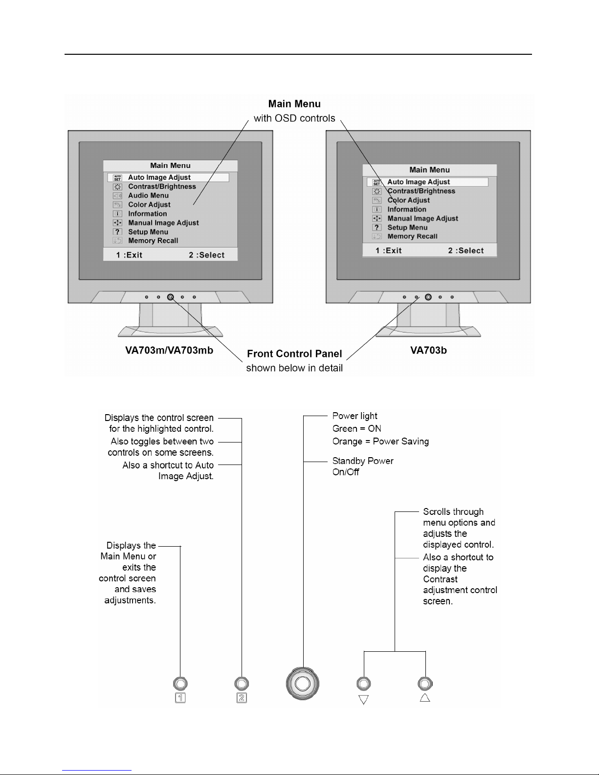
3. Front Panel Function Control Description
Use the buttons on the front control panel to display and adjust the OSD controls which display on the screen.
9
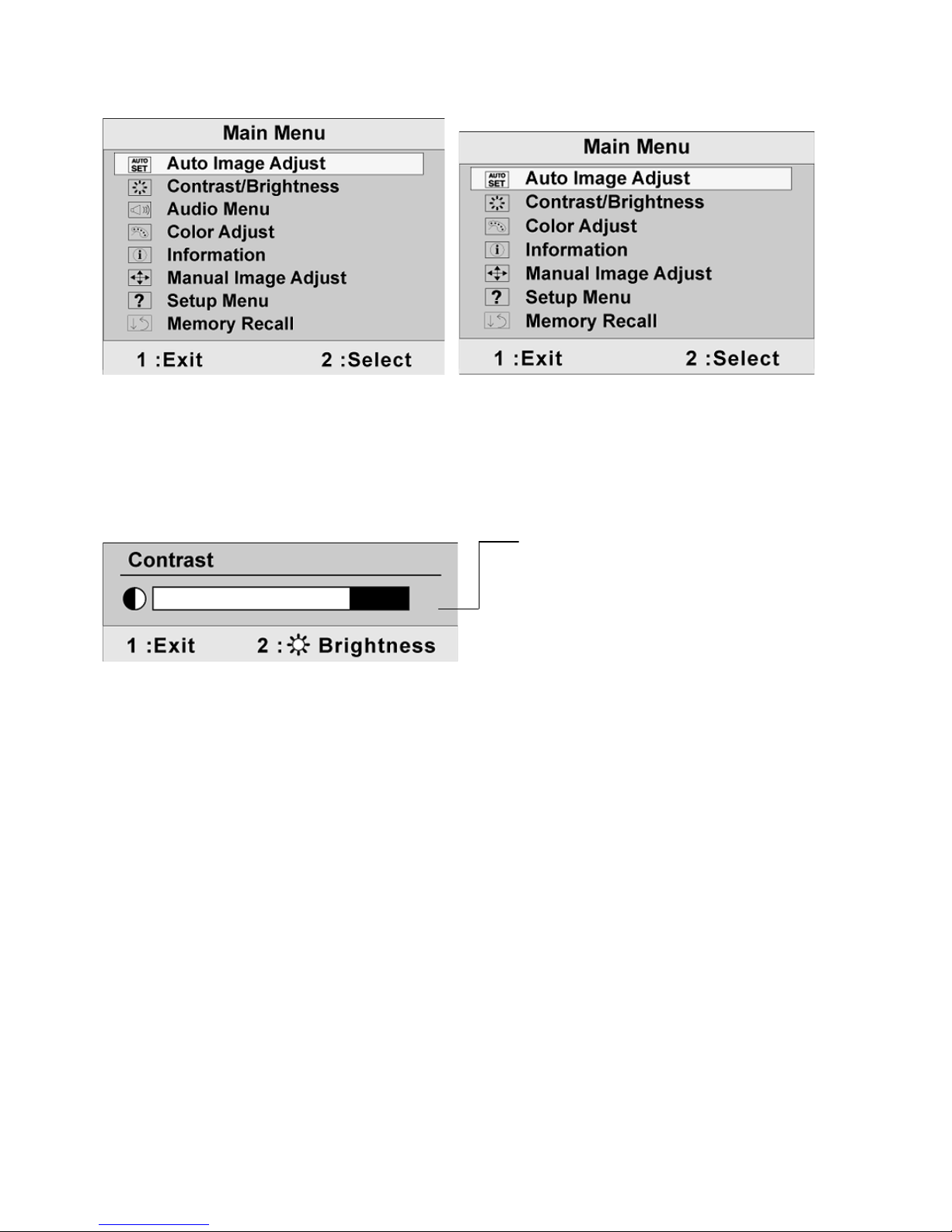
Do the following to adjust the display setting:
1. To display the Main Menu, press button [1].
VA703m/VA703mb VA703b
NOTE: All OSD menus and adjustment screens disappear automatically after about 15 seconds. This is adjustable
through the OSD timeout setting in the setup menu.
2. To select a control to adjust, press ▲ or▼ to scroll up or down in the Main Menu.
3. After the desired control is selected, press button [2]. A control screen like the one shown below appears.
4. To adjust the control, press the up ▲ or down ▼ buttons.
5. To save the adjustments and exit the menu, press button [1] twice.
The following tips may help you optimize your display:
• Adjust the computer's graphics card so that it outputs a 1280 x 1024 @ 60Hz video signal to the LCD display.
(Look for instructions on “changing the refresh rate” in the graphics card's user guide.)
• If necessary, make small adjustments using H. POSITION and V. POSITION until the screen image is completely
visible. (The black border around the edge of the screen should barely touch the illuminated “active area” of the LCD
display.)
The line at the bottom of the screen shows
the current functions of buttons 1 and 2:
Exit or select the Brightness control.
10
Main Menu Controls
Adjust the menu items shown below by using the up ▲ and down ▼ buttons.
Control Explanation
Control Explanation
Auto Image Adjust automatically sizes, centers, and fine tunes the video signal to eliminate
waviness and distortion. Press the [2] button to obtain a sharper image.
NOTE: Auto Image Adjust works with most common video cards. If this function does not work
on your LCD display, then lower the video refresh rate to 60 Hz and set the resolution to its
pre-set value.
Contrast adjusts the difference between the image background (black level) and the
foreground (white level).
Brightness adjusts background black level of the screen image.
Audio Adjust (For VA703m/VA703mb only)
Volume increases the volume, decreases the volume, and mutes the audio.
Mute temporarily silences audio output.
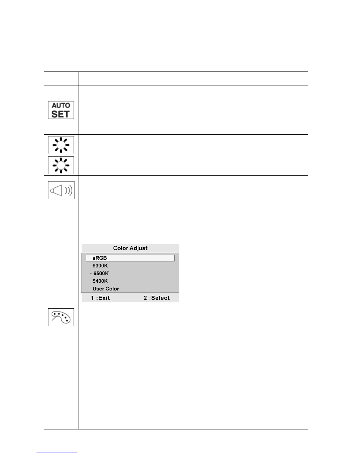
Color Adjust provides several color adjustment modes, including preset color temperatures
and a User Color mode which allows independent adjustment of red (R), green (G), and blue
(B). The factory setting for this product is 6500K (6500 Kelvin).
sRGB-This is quickly becoming the industry standard for color management, with support
being included in many of the latest applications. Enabling this setting allows the LCD display
to more accurately display colors the way they were originally intended. Enabling the intended.
Enabling the sRGB setting will cause Contrast and Brightness adjustments to be disabled.
9300K-Adds blue to the screen image for cooler white (used in most office
settings with fluorescent lighting).
6500K-Adds red to the screen image for warmer white and richer red.
5400K-Adds green to the screen image for darker color.
User Color Individual adjustments for red (R), green (G), and blue (B).

11
1. To select color (R, G or B) press button [2].
2. To adjust selected color, press ▲ and▼.
Important: If you select RECALL from the Main Menu when the product is
set to a Preset Timing Mode, colors return to the 6500K factory preset.
Information displays the timing mode (video signal input) coming from the graphics card in
the computer, the LCD model number, the serial number, and the ViewSonic
®
website URL.
See your graphics card’s user guide for instructions on changing the resolution and refresh
rate (vertical frequency). NOTE: VESA 1280 x 1024 @ 60Hz (recommended) means that the
resolution is 1280 x 1024 and the refresh rate is 60 Hertz.
Manual Image Adjust displays the Manual Image Adjust menu.
H./V. Position (Horizontal/Vertical Position) moves the screen image left or right and up or
down.
H. Size (Horizontal Size) adjusts the width of the screen image.
Fine Tune sharpens the focus by aligning text and/or graphics with pixel boundaries.
NOTE: Try Auto Image Adjust first.
Sharpness adjusts the clarity and focus of the screen image.
12
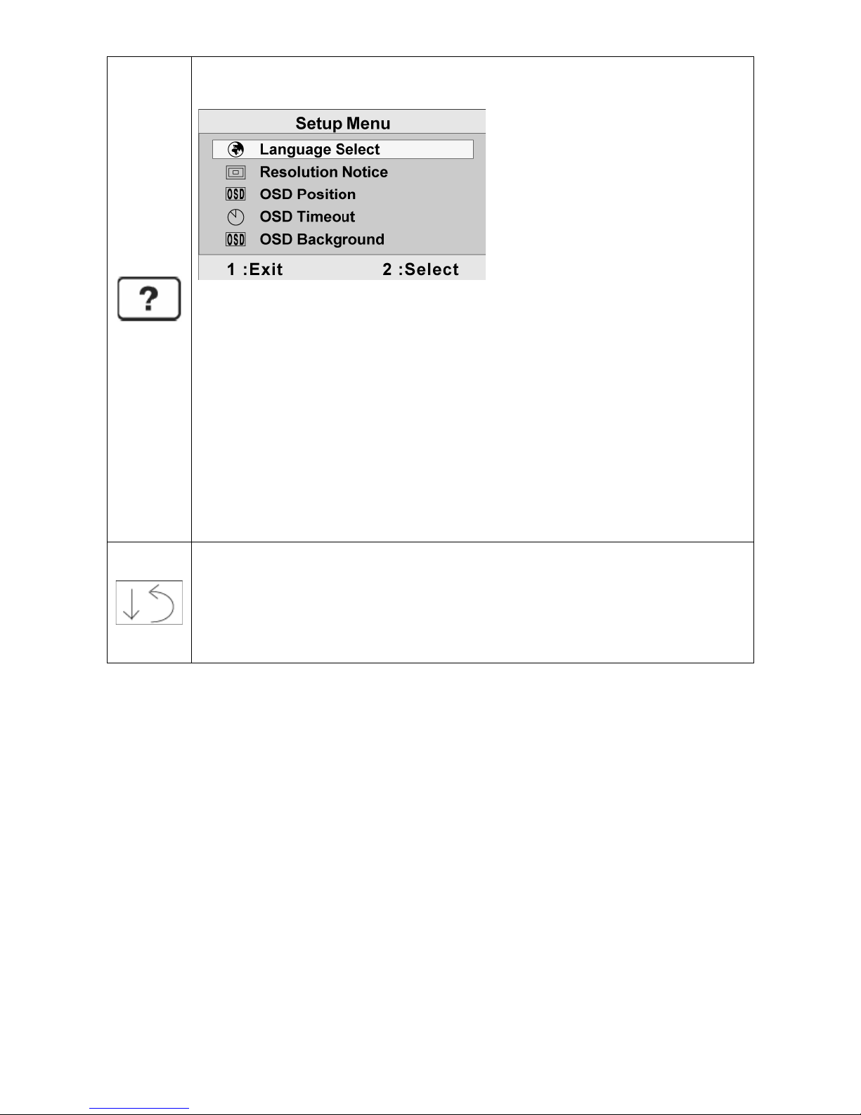
Setup Menu displays the menu shown below:
Language Select allows the user to choose the language used in the menus and control
screens.
Resolution Notice advises the optimal resolution to use.
OSD Position allows the user to move the OSD menus and control screens.
OSD Timeout sets the length of time the OSD screen is displayed. For example, with a “15
second” setting, if a control is not pushed within 15 seconds, the display screen disappears.
OSD Background allows the user to turn the OSD background On or Off.
Memory Recall returns the adjustments back to factory settings if the display is operating in a
factory Preset Timing Mode listed in the Specifications of this manual.
Exception: This control does not affect changes made with the User Color control, Language
Select or Power Lock setting.
13
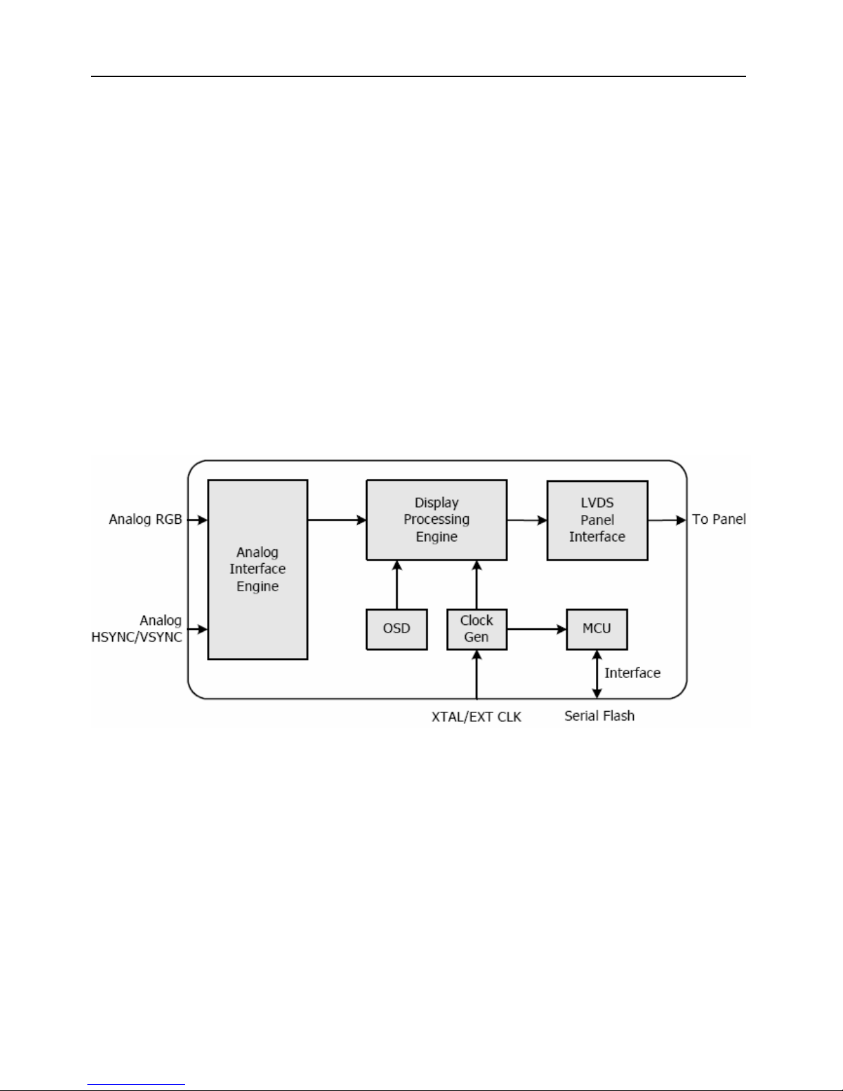
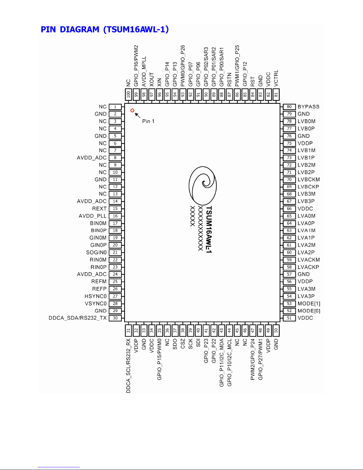
4. Circuit Description
4.1 Main Board
Scalar TSUM16AWL-1(U401)
The TSUM16AWL-1(U401) is total solution graphics processing IC for LCD monitors with panel resolutions up to
WXGA+/SXGA+. It is configured with a high-speed integrated triple-ADC/PLL, a high quality displayprocessing
engine, and an integrated output display interface that can support LVDS panel interface format.
To further reduce system costs, the TSUM16AL-1 also integrates intelligent power management control
capability for green-mode requirements and spread-spectrum support for EMI management.
The TSUM16AL-1 incorporates the world’s first coherent oversampled RGB graphics ADC in a monitor controller
system1. The oversampling ADC samples the input RGB signals at a frequency that is much higher than the
signal source pixel rate. This can preserve details in the video signal that ordinarily would be lost due to input
signal jitter or bandwidth limitations in non-oversampled systems.
The TSUM16AL-1 also incorporates a new Dynamic Frame Rate (DFR) generator2 for the digital output video to
the display panel that preserves the advantages of a fixed output clock rate, while eliminating the output end of
frame short-line.
Block Diagram
14
15
PIN Function:
Analog Interface
Pin Name Pin Type Function Pin
HSYNC0 Schmitt Trigger Input w/ 5V-tolerant Analog HSYNC input 27
VSYNC0 Schmitt Trigger Input w/ 5V-tolerant Analog VSYNC input 28
REFP InternalADC top de-coupling pin 26
REFM Internal ADC bottom de-coupling pin 25
RIN0P Analog Input Analog red input 23
RIN0M Analog Input Reference ground for analog red input 22
SOGIN0 Analog Input Sync-on-green input 21
GIN0P Analog Input Analog green input 20
GIN0M Analog Input Reference ground for analog green input 19
BIN0P Analog Input Analog blue input 18
BIN0M Analog Input Reference ground for analog blue input 17
REXT External resistor 390 ohm to AVDD_ADC 15
Serial Flash Interface
Pin Name Pin Type Function Pin
SDO Input w/ 5V-Tolerant SPI Flash Serial Data Output 37
CSZ Output SPI Flash Chip Select 38
SCK Output SPI Flash Serial Clock 39
SDI Output SPI Flash Serial Data Input 40
LVDS Interface
Pin Name Pin Type Function Pin
LVA0M Output A-Link Negative LVDS Differential Data Output 65
LVA0P Output A-Link Positive LVDS Differential Data Output 64
LVA1M Output A-Link Negative LVDS Differential Data Output 63
LVA1P Output A-Link Positive LVDS Differential Data Output 62
LVA2M Output A-Link Negative LVDS Differential Data Output 61
LVA2P Output A-Link Positive LVDS Differential Data Output 60
LVA3M Output A-Link Negative LVDS Differential Data Output 55
LVA3P Output A-Link Positive LVDS Differential Data Output 54
LVACKM Output A-Link Negative LVDS Differential Clock Output 59
16
Pin Name Pin Type Function Pin
LVACKP Output A-Link Positive LVDS Differential Clock Output 58
LVB0M Output B-Link Negative LVDS Differential Data Output 78
LVB0P Output B-Link Positive LVDS Differential Data Output 77
LVB1M Output B-Link Negative LVDS Differential Data Output 74
LVB1P Output B-Link Positive LVDS Differential Data Output 73
LVB2M Output B-Link Negative LVDS Differential Data Output 72
LVB2P Output B-Link Positive LVDS Differential Data Output 71
LVB3M Output B-Link Negative LVDS Differential Data Output 68
LVB3P Output B-Link Positive LVDS Differential Data Output 67
LVBCKM Output B-Link Negative LVDS Differential Clock Output 70
LVBCKP Output B-Link Positive LVDS Differential Clock Output 69
GPIO Interface
Pin Name Pin Type Function Pin
GPIO_P06
I/O w/ 5V-tolerant
General Purpose Input/Output; 6/12mA programmable driving
strength
91
GPIO_P07
I/O w/ 5V-tolerant
General Purpose Input/Output; 6/12mA programmable driving
strength
92
PWM0/ GPIO_P26 I/O w/ 5V-tolerant
Pulse Width Modulation Output; 4mA driving strength/ General
Purpose Input/Output; 4mA driving strength
93
GPIO_P13 I/O w/ 5V-tolerant General Purpose Input/Output; 4mA driving strength 94
GPIO_P14 I/O w/ 5V-tolerant General Purpose Input/Output; 4mA driving strength 95
GPIO_P16/ PWM2 I/O w/ 5V-tolerant
General Purpose Input/Output; 4mA driving strength/Pulse
Width Modulation Output; 4mA driving strength
99
GPIO_P15/ PWM0 I/O w/ 5V-tolerant
General Purpose Input/Output; 4mA driving strength/ Pulse
Width Modulation Output; 4mA driving strength
35
GPIO_P23 I/O w/ 5V-tolerant General Purpose Input/Output; 4mA driving strength 41
GPIO_P22 I/O w/ 5V-tolerant General Purpose Input/Output; 4mA driving strength 42
GPIO_P11/I2C_MDA I/O w/ 5V-tolerant
General Purpose Input/Output; 4mA driving strength/I2C Master
Data
43
GPIO_P10/I2C_MCL I/O w/ V-Tolerant
General Purpose Input/Output; 4mA driving strength/I2C Master
Clock
44
PWM2/ GPIO_P24 I/O w/ 5V-tolerant
Pulse Width Modulation Output; 4mA driving strength/ General
Purpose Input/Output; 4mA driving strength
47
GPIO_P27/ PWM1 I/O w/ 5V-tolerant
General Purpose Input/Output; 4mA driving strength/ Pulse
Width Modulation Output; 4mA driving strength
48
GPIO_P12 I/O w/ 5V-tolerant General Purpose Input/Output; 4mA driving strength 85

17
Pin Name Pin Type Function Pin
PWM1/GPIO_P25 I/O w/ 5V-tolerant
Pulse Width Modulation Output; 4mA driving strength/
General Purpose Input/Output; 4mA driving strength
86
GPIO_P00/SAR1 I/O w/ 5V-tolerant
General Purpose Input/Output; 4mA driving strength/
SAR ADC Input
88
GPIO_P01/SAR2 I/O w/ 5V-tolerant
General Purpose Input/Output; 4mA driving strength/
SAR ADC Input
89
GPIO_P02/SAR3 I/O w/ 5V-tolerant
General Purpose Input/Output; 4mA driving strength/
SAR ADC Input
90
Misc.Interface
Pin Name Pin Type Function Pin
BYPASS For External Bypass Capacitor 80
RST Input w/ 5V-Tolerant Chip Reset; High Reset 84
RSTN Input w/ 5V-Tolerant Chip Reset; Low Reset 87
VCTRL Output Regulator Control 81
Chip Configuration Input
MODE[1:0] Chip Operation
MODE[1:0] Input
00 Normal Operation
53,
52
DDCA_SDA/
RS232_TX
I/O w/ 5V-tolerant DDC Data for Analog Interface; 4mA driving
strength/ UART Transmitter/GPIO
30
DDCA_SCL/
RS232_RX
Input w/ 5V-Tolerant DDC Clock for Analog Interface/ UART
Receiver/GPIO
31
XIN Crystal Oscillator Input Xin 96
XOUT
Crystal Output Oscillator
Xout 97
Power Pins
Pin Name Pin Type Function Pin
AVDD_ADC 3.3V Power ADC Power 8, 14, 24
AVDD_PLL 3.3V Power PLL Power 16
AVDD_MPLL 3.3V Power MPLL Power 98
VDDP 3.3V Power Digital Output Power 32, 49, 56, 75
VDDC 1.8V Power Digital Core Power 34, 51, 66, 82
GND Ground Ground 2, 5, 11, 29, 33, 50, 57, 76, 79, 83
NC No Connect.Leave These Pins Floating 1,3,4,6,7,9,10,12,13,36,45,46,100
18
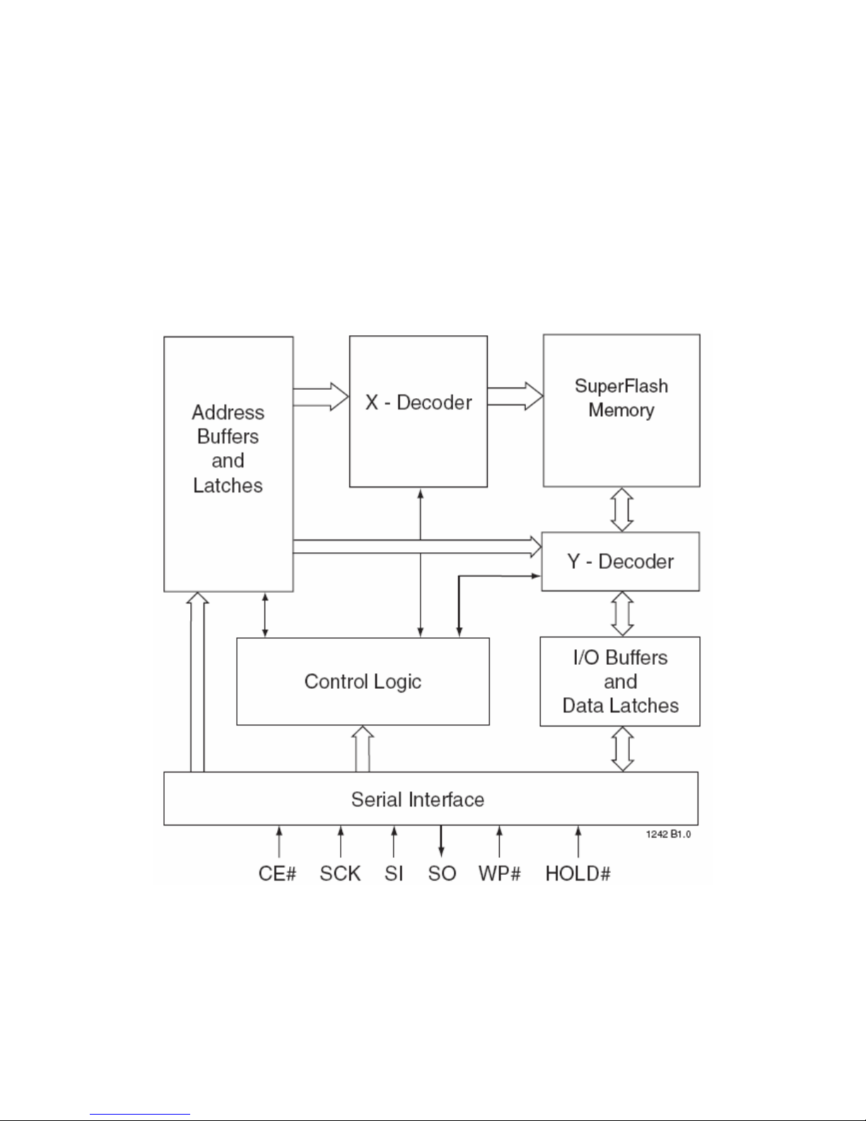
Flash Memory SST25LF020A/040A(U402)
The SST25LF020A is accessed through the SPI (Serial Peripheral Interface) bus compatible protocol. The
SPI bus consist of four control lines; Chip Enable (CE#) is used to select the device, and data is accessed through
the Serial Data Input (SI), Serial Data Output (SO), and Serial Clock (SCK).
The SST25LF020A supports both Mode 0 (0,0) and Mode 3 (1,1) of SPI bus operations. The difference
between the two modes, as shown in Figure 2, is the state of the SCK signal when the bus master is in Stand-by
mode and no data is being transferred. The SCK signal is low for Mode 0 and SCK signal is high for Mode 3. For
both modes, the Serial Data In (SI) is sampled at the rising edge of the SCK clock signal and the Serial Data Output
(SO) is driven after the falling edge of the SCK clock signal.
Block Diagram
19
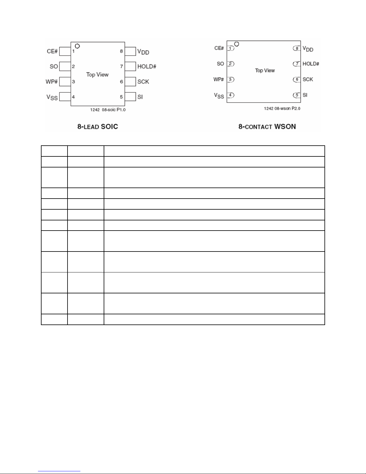
Pin Description
Symbol Pin Name Functions
SCK Serial Clock To provide the timing of the serial interface.
Commands, addresses, or input data are latched on the rising edge of the clock input,
while output data is shifted out on the falling edge of the clock input.
SI Serial Data To transfer commands, addresses, or data serially into the device.
Input Inputs are latched on the rising edge of the serial clock.
SO Serial Data To transfer data serially out of the device.
Output Data is shifted out on the falling edge of the serial clock.
CE# Chip Enable
The device is enabled by a high to low transition on CE#. CE# must remain low for the
duration of any command sequence.
WP#
Write
Protect
The Write Protect (WP#) pin is used to enable/disable BPL bit in the status register.
HOLD# Hold
To temporarily stop serial communication with SPI flash memory without resetting the
device.
VDD
Power
Supply
To provide power supply (3.0-3.6V).
VSS Ground
20
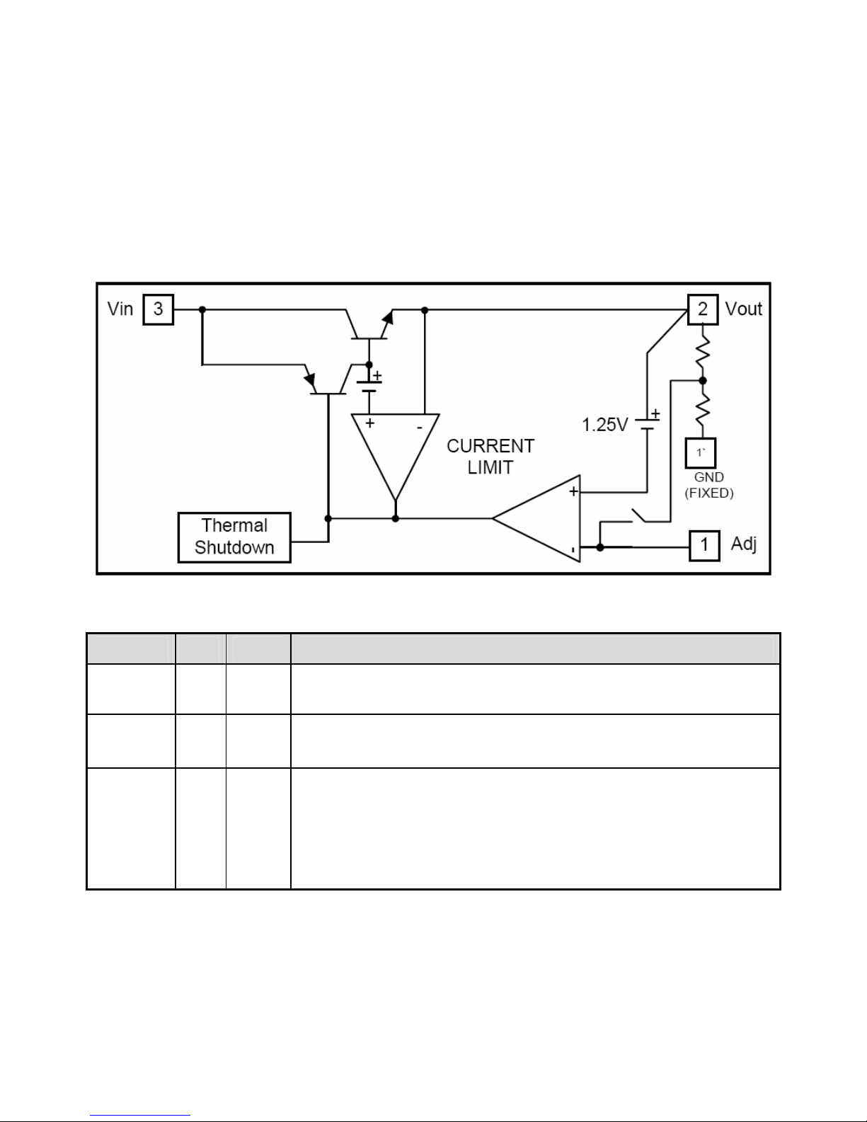
DC-DC AP1117E33L(U701)
AP1117 is a low dropout positive adjustable or fixed-mode regulator with minimum of 1A output current capability.
The product is specifically designed to provide well-regulated supply for low voltage IC applications such as
high-speed bus termination and low current 3.3V logic supply.
AP1117 is also well suited for other applications such as VGA cards. AP1117 is guaranteed to have lower than 1.4V
dropout at full load current making it ideal to provide well-regulated outputs of 1.25 to 5.0 with 6.4V to 12V input
supply.
Block Diagrm
Pin Descriptions
Name I/O Pin # Function
Adj (GND) I 1
A resistor divider from this pin to the Vout pin and ground sets the output voltage.
(Ground only for Fixed-Mode)
Vout O 2
The output of the regulator. A minimum of 10uF capacitor (0.15Ω ≤ESR ≤20Ω)
must be connected from this pin to ground to insure stability.
Vin I 3
The input pin of regulator. Typically a large storage capacitor (0.15Ω ≤ESR
≤20Ω) is connected from this pin to ground to insure that the input voltage does
not sag below the minimum dropout voltage during the load transient response.
This pin must always be 1.3V higher than Vout in order for the device to regulate
properly.
21
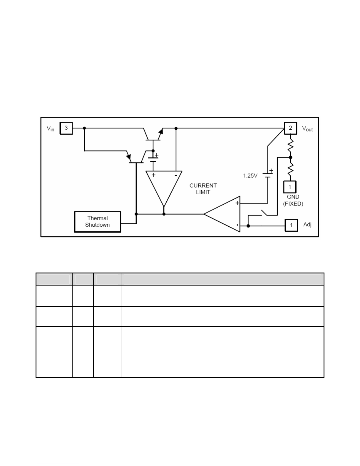
DC-DC AP1117E18LA (U702)
AP1117 is a low dropout positive adjustable or fixed-mode regulator with 1A output current capability. The product is
voltage specifically designed to provide well-regulated supply for low IC applications such as high-speed bus
termination and low current 3.3V logic supply.
AP1117 is also well suited for other applications such as VGA cards. AP1117 is guaranteed to have lower than 1.4V
dropout at full load current making it ideal to provide well-regulated outputs of 1.25 to 5.0 with 6.4V to 18V input
supply. AP1117 is available in both commercial and industrial temperature grade.
Block Diagrm
Pin Descriptions
Name I/O Pin # Function
Adj (GND) I 1
A resistor divider from this pin to the Voutpin and ground sets the output voltage
(Ground only for Fixed-Mode).
Vout O 2
The output of the regulator. A minimum of 10uF capacitor (0.15Ω ≤ESR ≤20Ω)
must be connected from this pin to ground to insure stability.
Vin I 3
The input pin of regulator. Typically a large storage capacitor (0.15Ω ≤ESR
≤20Ω) is connected from this pin to ground to insure that the input voltage does
not sag below the minimum dropout voltage during the load transient response.
This pin must always be 1.3V higher than Voutin order for the device to regulate
properly.
 Loading...