

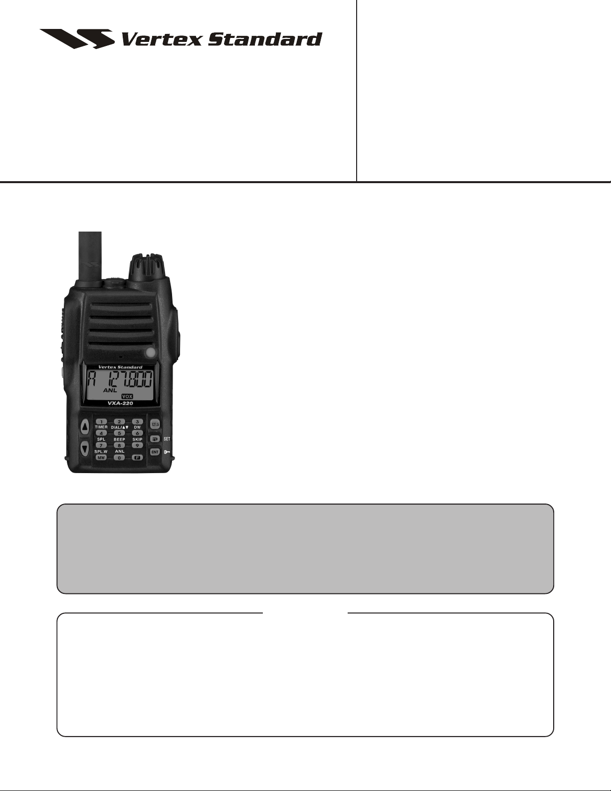
Air Band Transceiver
VXA-220
Service Manual
2006 VERTEX STANDARD CO., LTD. (EC072N90A)
©
Introduction
This manual provides technical information necessary for servicing the VXA220 Air Band Transceiver.
Servicing this equipment requires expertise in handling surface-mount chip
components. Attempts by non-qualified persons to service this equipment may
result in permanent damage not covered by the warranty, and may be illegal
in some countries.
VERTEX STANDARD CO., LTD.
4-8-8 Nakameguro, Meguro-Ku, Tokyo 153-8644, Japan
VERTEX STANDARD
US Headquarters
10900 Walker Street, Cypress, CA 90630, U.S.A.
YAESU EUROPE B.V.
P.O. Box 75525, 1118 ZN Schiphol, The Netherlands
YAESU UK LTD.
Unit 12, Sun Valley Business Park, Winnall Close
Winchester, Hampshire, SO23 0LB, U.K.
VERTEX STANDARD HK LTD.
Unit 5, 20/F., Seaview Centre, 139-141 Hoi Bun Road,
Kwun Tong, Kowloon, Hong Kong
VERTEX STANDARD (AUSTRALIA) PTY., LTD.
Normanby Business Park, Unit 14/45 Normanby Road
Notting Hill 3168, Victoria, Australia
Two PCB layout diagrams are provided for each double-sided circuit board in
the transceiver. Each side of thr board is referred to by the type of the majority
of components installed on that side (“leaded” or “chip-only”). In most cases
one side has only chip components, and the other has either a mixture of both
chip and leaded components (trimmers, coils, electrolytic capacitors, ICs, etc.),
or leaded components only.
While we believe the technical information in this manual to be correct, Vertex
Standard assumes no liability for damage that may occur as a result of typographical or other errors that may be present. Your cooperation in pointing
out any inconsistencies in the technical information would be appreciated.
Important Note
This transceiver was assembled using Pb (lead) free solder, based on the RoHS specification.
Only lead-free solder (Alloy Composition: Sn-3.0Ag-0.5Cu) should be used for repairs performed on this
apparatus. The solder stated above utilizes the alloy composition required for compliance with the lead-free
specification, and any solder with the above alloy composition may be used.
Contents
Specifications............................................................................................................................................................... 2
Exploded View & Miscellaneous Parts .................................................................................................................. 3
Block Diagram ............................................................................................................................................................. 5
Circuit Description ..................................................................................................................................................... 7
Alignment ..................................................................................................................................................................... 9
MAIN Unit Circuit Diagram .................................................................................................................................. 13
MAIN Unit Parts Layout ......................................................................................................................................... 15
MAIN Unit Parts List ............................................................................................................................................... 17
1

Specifications
General
Frequency Range: TX: 118.000 - 136.975 MHz,
RX: 108.000 - 136.975 MHz,
Weather Channels (WX-01 - WX-10: USA version only)
Channel Spacing: 25 kHz
Emission Type: TX: AM,
RX: AM & FM (FM: for receiving the Weather Channels, USA version only)
Supply Voltage: 6.0 - 15.0 VDC
Current Consumption (approx.): 250 μA (power off),
35 mA (battery saver on, saver ratio 1:5)
60 mA (squelch on),
200 mA (receive),
850 mA (transmit 1.5 W Carrier)
Temperature Range: +14 °F to + 140 °F (–10 °C to +60 °C)
Case Size (WxHxD): 2.36 x 4.09 x 1.2 inches (60 x 104 x 30.5 mm) w/o knob & antenna
Weight (approx.): 12.7 oz (360 grams) with FNB-83, antenna, and belt clip
Receiver
Circuit Type: Double-conversion superheterodyne
IFs: 47.25 MHz & 450 kHz
Sensitivity: AM: Better than 0.8 μV (for 6 dB S/N with 1 kHz, 30 % modulation)
FM; Better than 0.4 μV (for 12 dB SINAD)
Selectivity: More than 8 kHz/–6 dB
Adjacent CH. Selectivity: Less than 25 kHz/–60 dB
AF Output (Internal speaker): 0.7 W @ 16 Ohms, 10 % THD
Transmitter
Power Output (@ 7.2 V): 5 W (PEP), 1.5 W (Carrier Power)
Frequency Stability: Better than ±10 ppm (+14 °F to + 140 °F [–10 °C to +60 °C])
Modulation System: Low Level Amplitude Modulation
Spurious Emission: >60 dB below carrier
Int. Microphone Type: Condenser
Ext. Mic. Impedance: 150 Ohms
Specifications are subject to change without notice or obligation.
2
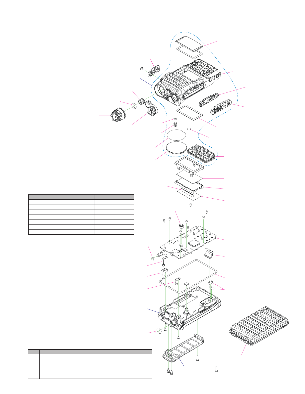
Exploded View & Miscellaneous Parts
RA0882500
WINDOW
RA0869100
EXT CAP
RA0786600
DOUBLE FACE (WINDOW)
RA0869000
KNOB (ENC)
ANTENNA ATV-10
NI-MH BATTERY FNB-83
OVERNIGHT CHARGER NC-88B
OVERNIGHT CHARGER NC-88C
CHARGER CRADLE CD-32
CABLE CT-96
BELT CLIP (ASSY
: Depends on transceiver version
Ú
Description
)
FRONT PANEL ASSY
SPECIAL NUT (VOL)
RA0768800
RUBBER CAP (MIC)
VXSTD P/N
Q3000194
AAD65X001
Ú
AAD88X002
Ú
AAD88X003
AAE82X001
Q7000451
AAC48X001
CP8817001
RA0777100
O RING
RA0866300
g
RA040160A
O RING
LIGHT GUIDE (LED)
RA0557900
RA0557900
SP NET
M4090168
SPEAKER
INTER CONNECTOR
Qty.
1
1
1
1
1
1
1
RA0769400
MIC HOLDER RUBBER
RA008890A
O RING
RA0869200
f
f
f
f
f
f
f
f
CP8817001
FRONT PANEL ASSY
RA0776700
HOLDER (PTT)
RA0776850A
RUBBER KNOB (PTT)
RA0787000
SPONGE RUBBER (WINDOW)
RA0337300
SHEET
RA0868900
RUBBER KNOB (17KEY)
RA077820A
LCD HOLDER
G6090178
LCD
RA0778100
LIGHT GUIDE
RA0809200
REFLECTOR SHEET
MAIN UNIT
REF.
c
d
e
f
g
VXSTD P/N
U02206027
U07230102
U24110002
U9900068
U9900181
TERMINAL PLATE (+IS)
TERMINAL HOLDER
TERMINAL PLATE (–)
w/TERMINAL PLATE (–)
PAN HEAD SCREW (M2X3NI #1)
DESCRIPTION
SEMS SCREW SM2.6X6SUS B
PAN HEAD SCREW M2X3NI #1
BIND HEAD TAPTITE-BM2X10NI
PAN HEAD TAPTITE-B M2X4NI#3
TAPTITE SCREW 2X3.5(CAP
RA0723400
RA010340B
RA035160A
CP8816001
REAR CASE ASSY
ELEC. COND TAPE
O RING
RA0844000
O RING
)
QTY.
2
1
2
9
1
c
f
d
e
AAE04X001
BELT CLIP ASSY
c
w/ SEMS SCREW (SM2.6X6SUS B)
e
RA055770B
LATCH NAIL C
RA0897500
RUBBER PACKING (CASE)
RA0918700 x2
ELEC. COND TAPE
AAD65X001
NI-MH BATTERY (FNB-83)
3

Exploded View & Miscellaneous Parts
4
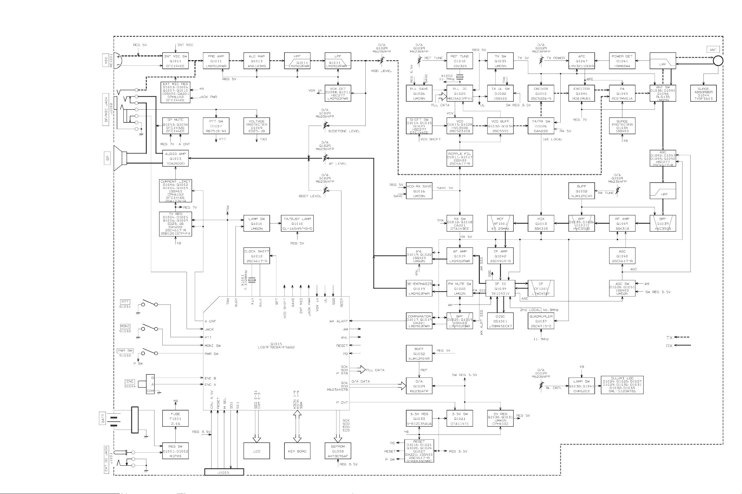
Block Diagram
5

Block Diagram
Note
6

Circuit Description
Receive Signal Path
Incoming RF from the antenna jack is passed through a
low-pass filter and high-pass filter consisting of coils
L1024, L1027, L1028, L1029, L1030 & L1031, capacitors
C1213, C1218, C1219, C1222, C1223, C1224, C1226, C1227,
C1228, C1229, C1230, & C1234 and antenna switching
diodes D1038 and D1040 (both RLS135) to the receiver
front end section.
Signals within the frequency range of the transceiver is
applied to the receiver front end which contains RF amplifier Q1049 (3SK318) and varactor-tuned band-pass filter consisting of coils L1014, L1015, L1018, L1021, L1025,
& L1026, capacitors C1180, C1182, C1184, C1185, C1186,
C1189, C1190, C1193, C1194, C1197, C1207, C1215, &
C1216, and diodes D1035, D1036, D1037, & D1039 (all
HVC350B), then applied to the 1st mixer Q1043 (3SK318).
Buffered output from the VCO is amplified by Q1032
(2SC5555ZD) to provide a pure 1st local signal between
155.25 and 184.25 MHz for injection to the 1st mixer. The
47.25 MHz 1st mixer product then passes through monolithic crystal filter XF1001 (7.5 kHz BW) which strips away
all but the desired signal, which is then amplified by mixer post-amp Q1042 (2SC4915).
The amplified 1st IF signal is applied to the AM/FM IF
subsystem IC Q1039 (TK10931), which contains the 2nd
mixer, 2nd local oscillator, limiter amplifier, noise amplifier and AM/FM detector.
A 2nd local signal is generated by PLL IC Q1025
(MB15A01PFV1) from the 11.7 MHz crystal X1002.
The11.7MHz signal is quadruple by Q1037 (2SC4915) to
produce the 450 kHz 2nd IF when mixed with the 1st IF
signal within Q1039 (TK10931). The 2nd IF then passes
through the ceramic filter CF1001 to strip away unwanted mixer products.
In the FM mode, a 2nd IF signal from the ceramic filter
CF1001 applied to the limiter amplifier section of Q1039
(TK10931), which removes amplitude variations in the
450 kHz IF before detection of the speech by the ceramic
discriminator CD1001. Detected audio from Q1039
(TK10931) is passed through the de-emphasis, consisting of the resistors R1082, R1087, R1089, & R1090, capacitors C1069, C1070, C1073, & C1081, and Q1019-2
(LM2902PWR).
In the AM mode, detected audio from Q1039 (TK10931)
is passed through the audio amplifier Q1019-1
(LM2902PWR) and ANL circuit, then applied to the AF
amplifier Q1019-2 (LM2902PWR). When impulse noise
received, a portion of the AM detector output signal from
the AM/FM IF subsystem Q1039 (TK10931), including
pulse noise is rectified by D1019 (1SS400). The resulting
DC is applied to the ANL MUTE gate Q1022 (UMG2N),
thus reducing the pulse noises.
The processed audio signal from Q1019-1 (LM2902PWR)
is passed through the amplifier Q1019-2 (LM2902PWR)
to the volume control IC Q1029 (M62364FP). The audio
signal is passed through the volume control IC to the audio power amplifier Q1003 (TDA2822), providing up to
0.7 Watts to 16 Ohm loudspeaker.
A portion of the AF signal from the AM/FM IF subsystem
Q1039 (TK10931VTL) converted into DC voltage within
the IC, and provide to the inversion amplifiers Q1048 and
Q1050 (both 2SC4617). These amplifier reduce the am-
plifier gain of the RF amplifier Q1049 (3SK318) while
receiving a strong signal.
Squelch Control
When signal is received, the DC squelch control voltage
appears at pin 15 of AM/FM IF subsystem Q1039
(TK10931) according to the receiving signal strength. This
DC is applied to pin 16 of microprocessor Q1015
(LC87F7C8A).
The DC squelch control voltage is compared with the SQL
threshold level by the microprocessor Q1015
(LC87F7C8A). If the DC squelch control voltage is lower,
the microprocessor Q1015 (LC87F7C8A) control pin 14
of volume control IC Q1029 (M62364FP) goes “LOW,”
thus disabling the AF audio. Also, the microprocessor
stops scanning, if active, and allows audio to pass through
the volume control IC Q1029 (M62364FP).
Transmit Signal Path
Speech input from the microphone is passed through the
microphone amplifier Q1011-1 (LM2902PWR), then ap-
plied to the ALC amplifier Q1013 (AN6123MS). The am-
plified speech signal is passed through the high-pass filter Q1011-4 (LM2902PWR) and low-pass filter Q1011-3
(LM2902PWR), which adjusts the modulation level, then
fed to the AM modulator Q1045 (RD07MVS1A).
When using the optional headset, pin 10 of microprocessor Q1015 (LC87F7C8A) goes “HIGH.” This signal is
applied to pin 15 of volume control IC Q1029 (M62364FP)
which allows amplified speech signals by the AF power
amplifier Q1001 (DTC144EE) as a monitor signal.
The carrier signal from the VCO Q1028 (2SC5231) passes through the buffer amplifier Q1032 (2SC5555) and TX/
RX switch D1026 (DAN222).
The signal from D1026 (DAN222) is amplified by Q1040
(2SC5226) and Q1044 (RD01MUS1), and ultimately applied to the final amplifier Q1045 (RD07MVS1A) which
increases the signal level up to 5 watts output power. The
7

Circuit Description
transmit signal then passes through the antenna switch
D1038 (RLS135), and is low-pass filtered to suppress
away harmonic spurious radiation before delivery to the
antenna.
Automatic Transmit Power Control
RF power output from the final amplifier is sampled by
C1217/C1221 and is rectified by D1041 (HSM88WA). The
resulting DC is fed through the Automatic Power Controller Q1047 (LMV321IDCKR), thus allowing control of
the power output.
Transmit Inhibit
When the transmit PLL is unlocked, pin 7 of PLL chip
Q1025 (MB15A01PFV1) goes to a logic “LOW.” The re-
sulting DC “Unlock” control voltage is switches off TX
inhibit switches Q1035 (UMD5N), to disable the supply
voltage to transmitter RF amplifiers Q1040 (2SC5226),
disabling the transmitter.
Spurious Suppression
Generation of spurious products by the transmitter is
minimized by the fundamental carrier frequency being
equal to the final transmitting frequency. Additional harmonic suppression is provided by a low-pass filter consisting of L1027, L1029, & L1031, and C1213, C1222, C1224,
C1227, C1229, & C1234, resulting in more than 60 dB of
harmonic suppression prior to delivery of the RF signal
to the antenna.
PLL Frequency Synthesizer
PLL circuitry consists of VCO Q1028 (2SC5231), VCO
buffer Q1032 & Q1034 (both 2SC5555), and PLL sub-
system IC Q1025 (MB15A01PFV1), which contains a ref-
erence divider, serial-to-parallel data latch, programmable divider, phase comparator and charge pump.
Stability is maintained by a regulated 3.5 V supply via
Q1033 (S-812C35AU) and 5V supply via Q1031
(CHP6102) which feeds the PLL reference oscillator Q1025
(MB15A01PFV1), as well as capacitors associated with
the 11.7 MHz frequency reference crystal X1002.
In the receive mode, VCO Q1028 (2SC5231) oscillates
between 155.25 and 184.25 MHz. The VCO output is buffered by Q1032 & Q1034 (both 2SC5555), and applied to
the prescaler section of Q1025 (MB15A01PFV1). There
the VCO signal is divided by 64 or 65, according to a control signal from the data latch section of Q1025
(MB15A01PFV1), before being applied to the programmable divider section of Q1025 (MB15A01PFV1). The
data latch section of Q1025 (MB15A01PFV1) also receives
serial dividing data from the microprocessor Q1015
(LC87F7BC8A), which causes the pre-divided VCO signal to be further divided in the programmable divider
section, depending upon the desired receive frequency,
so as to produce a 5 kHz derivative of the current VCO
frequency.
Meanwhile, the reference divider section of Q1025
(MB15A01PFV1) divides the 11.7 MHz crystal reference
from the reference oscillator section by 2340 to produce
the 5 kHz loop reference. The 5 kHz signal from the programmable divider (derived from the VCO) and that derived from the reference oscillator are applied to the phase
detector section of Q1025 (MB15A01PFV1), which pro-
duces a pulsed output with pulse duration depending on
the phase difference between the input signals. This pulse
train is filtered to DC and returned to the varactor D1013
(HVC350B).
Changes in the level of the DC voltage applied to the varactors affect the reactance in the tank circuit of the VCO,
changing the oscillating frequency of the VCO according
to the phase difference between the signals derived from
the VCO and the crystal reference oscillator. The VCO is
thus phase-locked to the crystal reference oscillator.
The output of the VCO Q1028 (2SC5231) is buffered by
Q1032 (2SC5555) before application to the 1st mixer, as
described previously.
For transmission, the VCO Q1028 (2SC5231) oscillates
between 118 and 137 MHz. The remainder of the PLL circuitry is shared with the receiver. However, the dividing
data from the microprocessor is such that the VCO frequency is at the actual transmit frequency (rather than
offset for IFs, as in the receiving case).
Receive and transmit buses select which VCO is made
active by Q1023 (DTC144EE).
When the power saving feature is active, the microprocessor periodically signals to the PLL IC Q1025
(MB15A01PFV1) to conserve power, and to shorten lockup time.
Push-To-Talk Transmit Activation
The PTT switch on the microphone is the control to pin 22
of microprocessor Q1015 (LC87F7BC8A), so that when
the PTT switch is closed, pin 31 of Q1015 (LC87F7BC8A)
goes “HIGH.” This signal cuts off the receiver by disabling
the 5 V supply bus at Q1018 (DTA143EE) which feeds
the front-end, FM IF subsystem IC Q1039 (TK10931VTL),
and receiver VCO circuitry. At the same time, Q1035
(UMD5N) activates the transmit 5 V supply line to enable
the transmitter.
8
Alignment
Introduction
The VXA-220 is carefully aligned at the factory for the
specified performance across the Aircraft and Weather
bands. Realignment should therefore not be necessary
except in the event of a component failure.
The following procedures cover the adjustments that are
not normally required once the transceiver has left the
factory. However, if damage occurs and some parts subsequently are replaced, realignment may be required. If a
sudden problem occurs during normal operation, it is likely due to component failure; realignment should not be
done until after the faulty component has been replaced.
We recommend that servicing be performed only by authorized Vertex Standard service technicians who are experienced with the circuitry and fully equipped for repair and alignment. If a fault is suspected, contact the
dealer from whom the transceiver was purchased for instructions regarding repair. Under no circumstances
should any alignment be attempted unless the normal
function and operation of the transceiver are clearly understood, the cause of the malfunction has been clearly
pinpointed and any faulty components replaced, and realignment determined to be absolutely necessary. Problems caused by unauthorized attempts at realignment are
not covered by the warranty policy
Vertex Standard reserves the right to change circuits and
alignment procedures, in the interest of improved performance, without notifying owners.
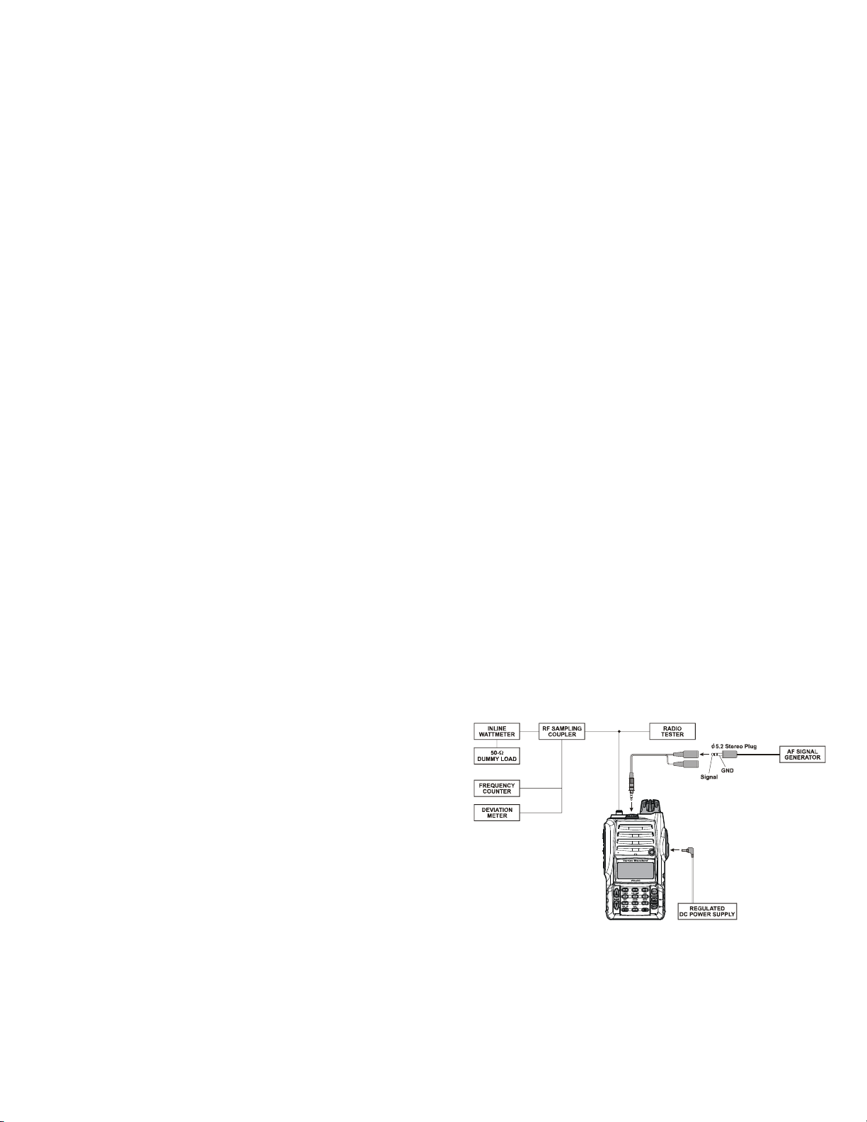
The following test equipment (and familiarity with its use)
is necessary for complete realignment. While most steps
do not require all of the equipment listed, the interactions
of some adjustments may require that more complex adjustments be performed afterwards. Do not attempt to
perform only a signal step unless it is clearly isolated electrically from all other steps. Have all test equipment ready
before beginning, and follow all of the steps in a section
in the order presented.
Required Test Equipment
Radio Tester with calibrated output level at 200 MHz
In-line Wattmeter with 5 % accuracy at 200 MHz
50 Ohm, 10 W RF Dummy Load
Regulated DC Power Supply adjustable from 3 to 15
VDC, 2 A
Frequency Counter: ±0.2 ppm accuracy at 200 MHz
AF Signal Generator
AC Voltmeter
DC Voltmeter: high impedance
VHF Sampling Coupler
Alignment Preparation & Precautions
A 50 Ohm RF load and in-line wattmeter must be connected to the main antenna jack in all procedures that call
for transmission, except where specified otherwise. Correct alignment is not possible with an antenna. After completing one step, read the next step to see if the same test
equipment is required. If not, remove the test equipment
(except dummy load and wattmeter, if connected) before
proceeding.
Correct alignment requires that the ambient temperature
be the same as that of the transceiver and test equipment,
and that this temperature be held constant between 20 30 °C (68 - 86 °F). When the transceiver is brought into the
shop from hot or cold air, it should be allowed some time
to come to room temperature before alignment. Whenever possible, alignments should be made with oscillator
shields and circuit boards firmly affixed in place. Also,
the test equipment must be thoroughly warmed up before beginning.
Set up the test equipment as shown below for transceiver
alignment, apply 7.2 VDC power to the transceiver.
Correction of problems caused by misalignment resulting from use of improper test equipment is not covered
under the warranty policy.
F
Notes: signal levels in dB referred to in alignment are
based on 0 dBμ = 0.5 μV (closed circuit).
9
 Loading...