

Vertex Standard VX-210AU Service Manual
VX-210AU
UHF Band
Service Manual
©2002 VERTEX STANDARD CO., LTD. Printed in Japan.
EC020U90A
VERTEX STANDARD CO., LTD.
4-8-8 Nakameguro, Meguro-Ku, Tokyo 153-8644, Japan
VERTEX STANDARD
US Headquarters
10900 Walker Street, Cypress, CA 90630, U.S.A.
International Division
8350 N.W. 52nd Terrace, Suite 201, Miami, FL 33166, U.S.A.
YAESU EUROPE B.V.
P.O. Box 75525, 1118 ZN Schiphol, The Netherlands
YAESU UK LTD.
Unit 12, Sun Valley Business Park, Winnall Close
Winchester, Hampshire, SO23 0LB, U.K.
VERTEX STANDARD HK LTD.
Unit 5, 20/F., Seaview Centre, 139-141 Hoi Bun Road,
Kwun Tong, Kowloon, Hong Kong
Introduction
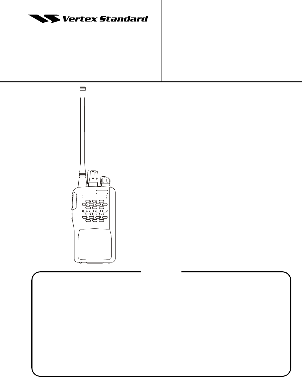
The Vertex VX-210AU is a compact hand portable transceiver for the UHF land mobile band that offers the convenience of small size, light weight, and simple operation.
The VX-210AU can be simply programmed by your
Vertex Dealer with up to 16 channels for single and split
frequency operation. The VX-210AU provides up to 5
watts of RF output power and includes a flexible quickconnect antenna.
The transceiver and Ni-Cd battery packs are constructed of thick high-impact polycarbonate plastic, with special attention paid by the designers to tight seals and ruggedness, assuring years of reliable operation even in harsh
environments.
The following pages describe the operation, features
and accessories of the VX-210AU. With proper care and
operation, the transceiver will provide many years of reliable communications.
Contents
Operating Manual Reprint .........................................................................................................................................2
Specifications ...............................................................................................................................................................5
Cloning.......................................................................................................................................................................... 6
Exploded View & Miscellaneous Parts .....................................................................................................................7
Block Diagram..............................................................................................................................................................8
Circuit Description ......................................................................................................................................................9
Alignment...................................................................................................................................................................11
Board Units (Schematics, Layouts & Parts)
MAIN Unit .............................................................................................................................................................13
SW Unit ................................................................................................................................................................... 37
Optional Board Units (Schematics, Layouts & Parts)
VTP-50 VX-Trunk Unit .......................................................................................................................................... 38
FVP-25 Encryption / DTMF Pager Unit ................................................................................................................ 40
1
Operating Manual Reprint
VOL
7
1
5
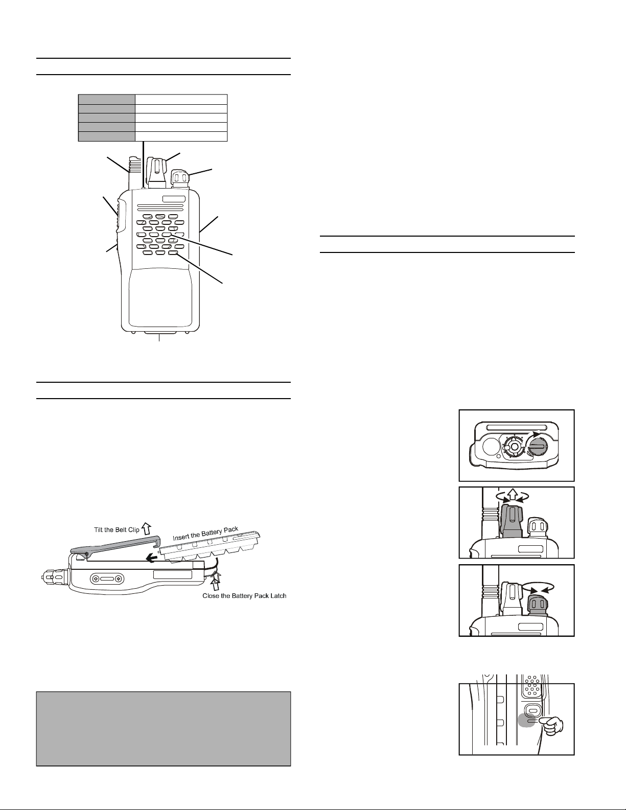
Contorols & Connectors
LED Indicator
Glows Green ACC on
Blinking Green Busy Channel (or SQL off)
Glows Red Transmitting
Blinking Red Battery Voltage is low
Blinking Yellow Receiving a Selective Call
Antenna
Push To Talk
(
PTT) Switch
ACC Button
Battery Pack
Latch
CH (Channel) Selector
VOL/PWR Knob
MIC/SP Jack
(
External Mic/Earphone
Speaker
Microphone
Before You Begin
Battery Pack Installation and Removal
r To install the battery, hold the transceiver with your
left hand, so your palm is over the speaker and your
thumb is on the top of the belt clip. Insert the battery
pack into the battery compartment on the back of the
radio while tilting the Belt Clip outward, then close
the Battery Pack Latch until it locks in place with a
“Click.”
Low Battery Indication
r As the battery discharges during use, the voltage gradu-
ally becomes lower. When the battery voltage reaches
6.3 volts, substitute a freshly charged battery and recharge
the depleted pack. The TX/BUSY indicator on the top of
the radio will blink red when the battery voltage is low.
r Avoid recharging Ni-Cd batteries often with little use
between charges, as this can degrade the charge capacity. We recommend that you carry an extra, fullycharged pack with you so the operational battery may
)
be used until depletion (this “deep cycling” technique
promotes better long-term battery capacity).
Operation
Preliminary Steps
r Install a charged battery pack onto the transceiver, as
described previously.
r Screw the supplied antenna onto the Antenna jack.
Never attempt to operate this transceiver without an
antenna connected.
r If you have a Speaker/Microphone, we recommend that
it not be connected until you are familiar with the basic operation of the VX-210A.
Operation Quick Start
r Turn the top panel’s VOL/
PWR knob clockwise to
turn on the radio on.
r Pull and turn the top
panel’s CH selector knob
to choose the desired operating channel.
1
1
9
CH
1
3
3
1
r Rotate the VOL/PWR knob
to set the volume level. If no
signal is present, press and
hold in the ACC button (the
r To remove the battery, turn the radio off and remove
any protective cases. Open the Battery Pack latch on
the bottom of the radio, then slide the battery downward and out from the radio while holding the Belt
Clip.
lower button on the left
side) for more than 1 second
(when “MONITOR” is assigned to the ACC button); background noise will now be heard, and you may use this to set
the VOL/PWR knob for the desired audio level.
r Press and hold in the ACC
button (when “MONI-
Caution!
Do not attempt to open any of the rechargeable NiCd packs, as they could explode if accidentally shortcircuited.
TOR” is assigned to the
ACC button) for more
than 1 second (or press the
ACC button twice) to
quiet the noise and resume normal (quiet) monitoring.
2
Operating Manual Reprint
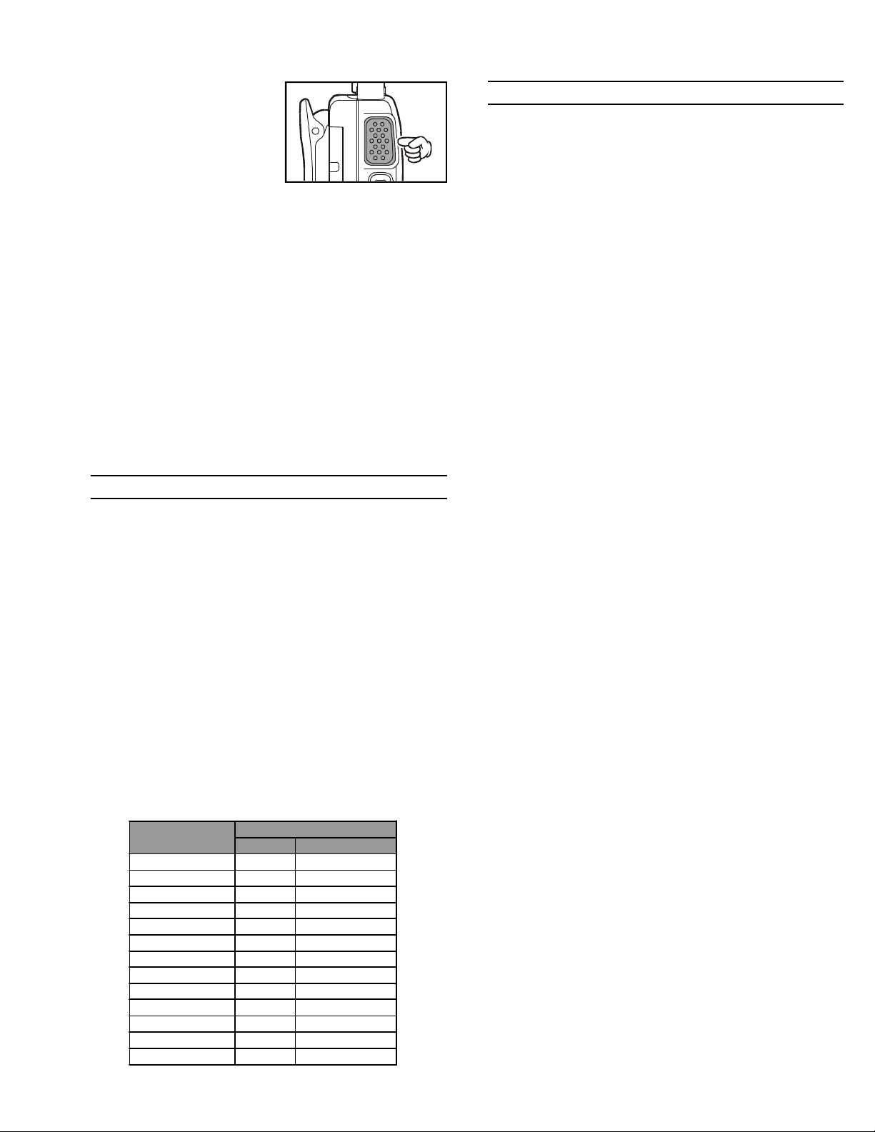
r To transmit, press and hold
in the PTT switch. Speak
into the microphone area
of the front panel grille
(lower left-hand corner) in
a normal voice level. To return to the Receive mode, release the PTT switch.
r If a Speaker/Microphone is available, remove the plas-
tic cap and its two mounting screws from the right side
of the transceiver, then insert the plug from the Speaker/
Microphone into the MIC/SP jack; secure the plug using the screws supplied with the Speaker/Microphone.
Hold the speaker grille up next to your ear while receiving. To transmit, press the PTT switch on the
Speaker/Microphone, just as you would on the main
transceiver’s body.
Note:
Save the original plastic cap and its mounting screws.
They should be re-installed when not using the
Speaker/Microphone.
Key Functions
The VX-210A provides a programmable “ACC” (Accessory)
button. The ACC button’s functions can be customized (set to
any of a variety of functions), via programming by your VER-
TEX STANDARD dealer, to meet your communications/network requirements. The particular function to be activated or
disabled may require a simple press of the ACC button, or it
may require that the ACC button be pressed and held in for one
second (or more). See the discussion below.
Some features may require the purchase and installation of
optional internal accessories.
The possible ACC button programming features are illustrated
below, and their functions are explained in the next chapter. For
further details, contact your VERTEX STANDARD dealer.
For future reference, check the box next to the function that
has been assigned to the ACC button on your particular radio,
and keep it handy.
Function
None
Monitor
Squelch OFF
Low Power
Scan
Follow-me Scan
Dual Watch
Talk Around
Call/Reset
Speed Dial
TX Save Off
ACC 1
ACC 2
ACC button
Press Press and Hold
Description of Operating Functions
Monitor
Press the ACC button to override (disable) the Tone Squelch.
Background noise or incoming signals will now be
heard whether or not a matching tone is present on the
signal. Press the ACC button once more to resume normal (quiet) Tone Squelch action.
Squelch OFF
Press the ACC button to override both the Noise and
Tone squelch systems. Again press the ACC button to
resume normal (quiet) Noise and Tone squelch action.
Low Power
Press the ACC button to set the radio's transmitter to
the “Low Power” mode, thus extending battery life.
Press the ACC button again to return to “High Power”
operation when in difficult terrain.
Scan
The Scanning feature is used to monitor multiple channels programmed into the transceiver. While scanning,
the radio will check each channel for the presence of a
signal, and will stop on a channel if a signal is present.
r To activate scanning:
Press the ACC button.
The scanner will search the channels, looking for
“active” ones; it will pause each time it finds a channel on which someone is speaking.
r To stop scanning:
Press the ACC button.
Operation will revert to the channel to which the
CH knob is set.
Follow-Me Scan
“Follow-Me” Scan feature checks a User-assigned Priority Channel regularly as you scan the other channels.
Thus, if only Channels 1, 3, and 5 (of the 8 available channels) are designated for “Scanning,” the user may nonetheless assign Channel as the “User-assigned” Priority
Channel via the “Follow-Me” feature.
Press the ACC button to activate “Follow-Me” scanning,
then pull and turn the CH selector knob to the channel
which you want to designate as the “User-Assigned Priority Channel”. When the scanner stops on an “active”
channel, the User-assigned Priority Channel will automatically be checked every few seconds.
Dual Watch
The Dual Watch feature is similar to the Scan feature,
except that only two channels are monitored: the current operating channel, and the “Priority” channel.
r To activate Dual Watch:
Press the ACC button.
The scanner will search the two channels; it will
pause each time it finds a channel on which someone is speaking.
3

Operating Manual Reprint
r To stop Dual Watch:
Press the ACC button.
Operation will revert to the channel to which the
CH knob is set.
Talk Around
Press the ACC button to activate the Talk Around feature when you are operating on duplex channel systems (separate receive and transmit frequencies, utilizing a “repeater” station). The Talk Around feature
allows you to bypass the repeater station and talk directly to a station that is nearby. This feature has no
effect when you are operating on “Simplex” channels,
where the receive and transmit frequencies are already
the same.
Note that your dealer may have made provision for
“Talk Around” channels by programming “repeater”
and “Talk Around” frequencies on two adjacent channels. If so, the ACC key may be used for one of the
other Pre-Programmed Functions.
Call/Reset
When the 2-tone selective calling unit is installed, press
the ACC button to silence the receiver and reset for
another call, when a communication is finished.
Speed Dial
Your Dealer may have pre-programmed Auto-Dial telephone number memories into your radio.
To dial a number, just press the Dealer-assigned ACC
button for Speed Dialing. The DTMF tones sent during the dialing sequence will be heard in the speaker.
TX Save Off
Press the ACC button to disable the Transmit Battery
Saver, if you are operating in a location where high
power is almost always needed.
The Transmit Battery Saver helps extend battery life
by reducing transmit power when a very strong signal
from an apparently nearby station is being received.
Under some circumstances, though, your hand-held
radio may not be heard well at the other end of the
communication path, and high power may be necessary at all times.
ACC 1
Activates an optional Unit (module) while the ACC
button is held depressed.
When you release the ACC button, the optional Unit
will be disabled.
For further details, contact your VERTEX STANDARD
dealer.
ACC 2
Toggles the optional Unit “on” or “off” whenever you
press the ACC button.
For example, when the optional “FVP-25” voice encryption unit is installed, press the ACC button momentarily to disable the voice encryption feature temporarily.
Press the ACC button again to re-enable the voice encryption feature.
Accessories & Options
FNB-V57 7.2 V 1100 mAh Ni-Cd Battery Pack
FNB-V57IS 7.2 V 1100 mAh Ni-Cd Intrinsically safe Battery
FBA-25 Alkaline Battery Case (6 x AA)
NC-76B 120 VAC Wall Charger
NC-76C 230-240 VAC Wall Charger
VAC-6400 6-Unit Multi charger
VAC-400B 120 VAC Desktop Rapid Charger
VAC-400C 230-240 VAC Desktop Rapid Charger
VCM-1 Mobile Mounting Bracket for VAC-400
MH-45B4B Speaker/Microphone
MH-37A4B Earpiece/Microphone
VC-25 VOX Headset
FVP-25 Encryption /DTMF Page Unit
VTP-50 VX-Trunk Unit
CT-42 PC-Programming Cable (CT-28 + CT-29)
CT-27 Cloning Cable (Set-to-Set Cloning)
FTT-17 16 keypad for VX-Trunk (VTP-50 required)
LCC-210 Leather Case
4

Specifications
General
Frequency Range: 400-430 MHz (AS1), 440-470 MHz (CS), 450-485 MHz (D), 485-512 MHz (F)
Number of Channels: 16 channels
Channel Spacing: 12.5/25 kHz
PLL Steps: 5/6.25 kHz
Power Supply Voltage: 7.5 V DC ±20 %
Battery Life (5-5-90 duty): 7.1 hrs. (8.5 hrs. w/saver) @5 W
Operating Temperature Range: –22° F to +140° F (–30° C to +60° C)
Frequency Stability: ±2.5 ppm
Dimensions: 4.21" (W) × 2.28" (H) × 1.0" (D) (108 × 58 × 26 mm)
Weight (Approx): 0.75 lb. (340 g) w/FNB-V57
Receiver (Measurements made per EIA standard TIA/EIA-603)
Sensitivity:
Adjacent Channel Selectivity: 65 dB (25 kHz)/60 dB (12.5 kHz)
Intermodulation: 65 dB
Spurious and Image Rejection: 65 dB
Hum & Noise: 45 dB
Audio Output: 500 mW @4 Ohms, 5% THD
EIA 12 dB SINAD: 0.25 µV
20 dB Quieting: 0.35 µV
Transmitter (Measurements made per EIA standard TIA/EIA-603)
Power Output: 5 / 1 W (Selectable) or 3.5 / 1 W (Selectable) w/FBA-25
Modulation: 16K0F3E / 11K0F3E (Direct FM)
Conducted Spurious Emission: 60 dB Below Carrier
FM Hum & Noise: 40 dB (25 kHz) / 35 dB (12.5kHz)
Audio
Distortion
Specifications subject to change without notice or obligation.
(@1 kHz):
< 5 %
5
Cloning
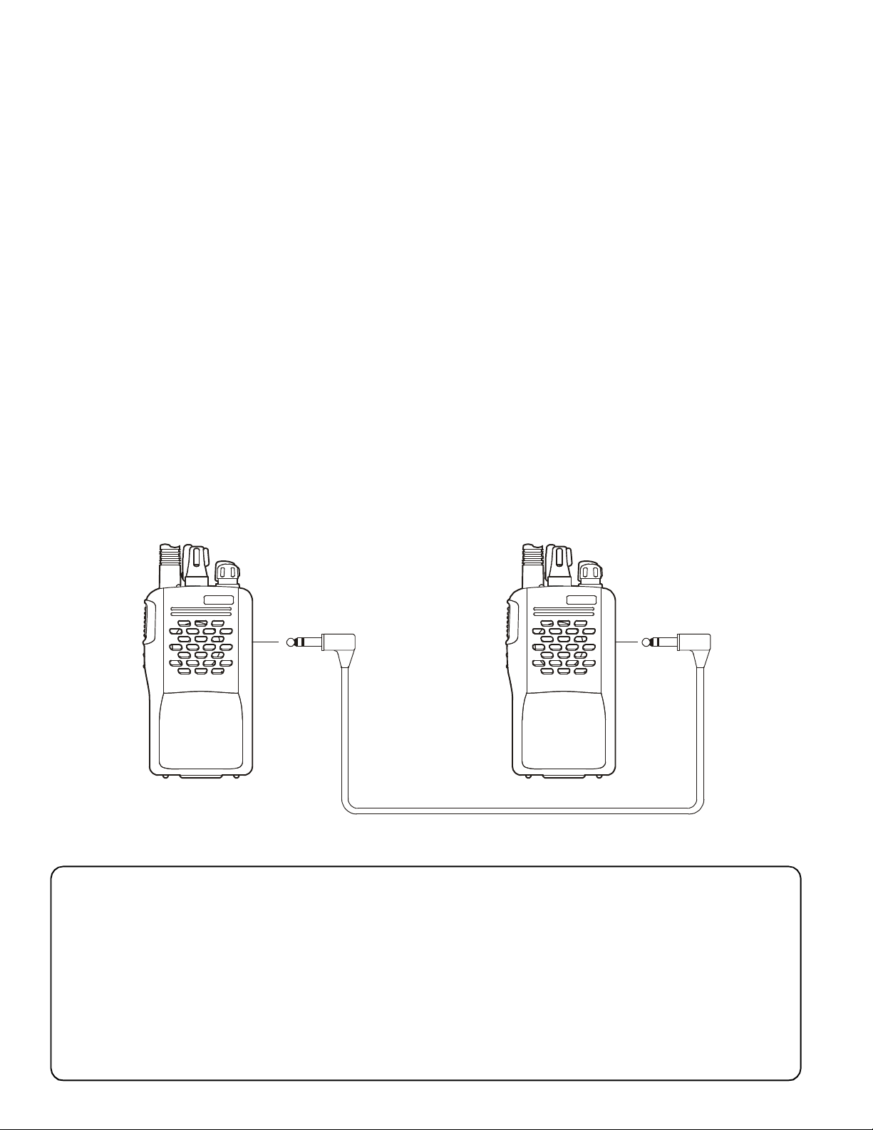
The VX-210A includes a convenient “Clone” feature,
which allows the programming data from one transceiver to be transferred to another VX-210A. Here is
the procedure for Cloning one radio’s data to another.
Note: When a cloning isn't made, you correct the following part using "CE45."
When a "Set-to-Set Clone" which is in the "Miscellaneous" menu is "Disabled," change this menu to
"Enabled."
1. Turn both transceivers off.
2. Remove the plastic cap and its two mounting
screws from the MIC/SP jack on the right side
of the transceiver. Do this for both transceivers.
3. Connect the optional CT-27 cloning cable between the MIC/SP jacks of the two transceivers.
4. Press and hold the PTT switch and ACC button
(just below the PTT switch) while turning the
transceiver on. Do this for both transceivers (the
order of the switch-on does not matter).
5. On the Destination transceiver, press the ACC
button (LED indicator will glow green).
6. Now, on the source transceiver, Press the PTT
switch.Data will now be transferred to the Des-
tination transceiver from the source transceiver (LED indicator will glow red).
7. If there is a problem during the cloning process,
LED indicator will blink red from source the
transceiver.
Check your cable connections and battery voltage, and try again.
8. If cloning is a successful, LED indicator will be
disappeared, turn the Destination transceiver
off. Now turn the source transceiver off.
9. Disconnect the CT-27. Replace the plastic cap
and its two mounting screws.
10. You can then turn the transceivers back on, and
begin normal operation.
Optional Cloning Cable CT-27
Dealer Programming of VTP-50
These procedures are designed to be used by the installing technician after the VTP-50 has been installed in the transceiver. To program a VX-210A's VTP-50 board, you will need the CT-42 program-
ming interface cable, the CE26 Programming diskette, and an IBM PC/AT or PS/2-compatible tyoe
computer.
To enter the Programming mode, use the following procedure:
1. Turn the transceiver off.
2. Turn on the transceiver while holding in the ACC button (just below the PTT switch).
6
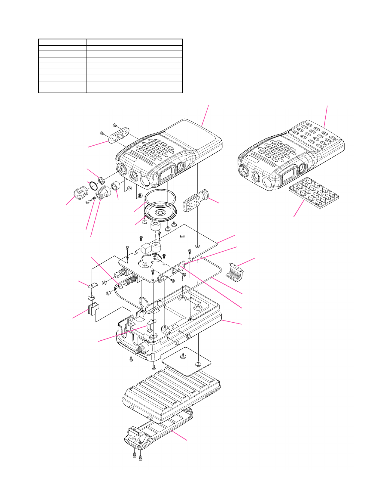
Exploded View & Miscellaneous Parts
REF. VXSTD P/N
U07230107
À
U20204007
Á
U02206007
Â
U9900051
Ã
U9900063
Ä
U9900068
Å
U9900086
Æ
U9900084
Ç
PAN HEAD SCREW M2x3B #1
BINDING HEAD SCREW M2.6x4B
SEMS SCREW SM2.6x6B
TAPTITE SCREW M2x4B #3
TAPTITE SCREW M2x3.3Ni
TAPTITE SCREW M2x4Ni #3
TAPTITE SCREW M1.7x2.5B
BINDING HEAD SCREW M2x7.5B
Description
Non-designated parts are available only
as part of a designated assembly.
Á
Á
RA0173500
CAP
RA0111400
RING NUT
RA008920A
RA008920B (Lot. 7~)
O RING
RA010300A
RA010300B (Lot. 12~)
KNOB
RA0112300
COIL SPRING
Ç
RA0228800
KNOB
RA008890A
O RING
RA0111500
SPECIAL NUT
R3152420
O RING
M4090128
SPEAKER
Å
Ä
Å
Ä
Å
Å
Qty.
1
2
2
1
5
6
2
1
RA018500A Vertex (USA)
RA018510A (EXP)
FRONT CASE ASS'Y
Ä
Å
RA0173400
RUBBER KNOB
MAIN Unit
SW Unit
RA018520A Vertex (USA)
RA018530A (EXP)
FRONT CASE ASS'Y (16KEY)
RA0123500
LATCH NAIL
RA0173700
RUBBER KNOB (16KEY)
RA0107000
TERMINAL PLATE R
RA010340A
TERMINAL HOLDER
RA0106900
TERMINAL PLATE L
Ã
Â
Â
Å
À
Æ
Æ
Ä
Ä
CP7140001
BELT CLIP ASS'Y
RA011070A
RUBBER PACKING
RA011720A
MYLAR SHEET
CP7139001
REAR CASE ASS'Y
7
7
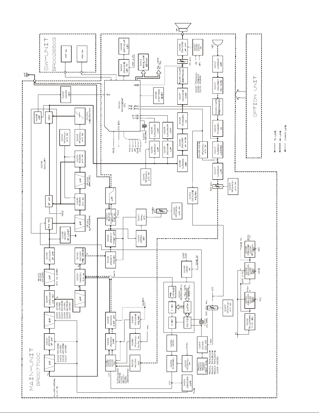
Block Diagram
8

Circuit Description
1. Receive Signal Path
Incoming RF from the antenna jack is delivered to the
RF Unit and passes through a low-pass filter consisting of
coils L1003, L1006 and L1007, capacitors C1002, C1007,
C1013, C1017, C1022, C1025, and C1169 and antenna
switching diode D1007 (RLS135).
Signals within the frequency range of the transceiver
enter a varactor-tuned band-pass filter consisting of coils
L1014 and L1015, capacitors C1057, C1058, C1064, C1071
and C1073, and diodes D1012 (HVC355B), D1013
(1SV280), D1016 (HVC355B) and D1017 (1SV280). The
signals are then amplified by Q1015 (2SC5006), and enter a varactor-tuned band-pass filter consisting of coils
L1018, L1021 and L1024, capacitors C1084, C1088, C1089,
C1094, and C1096, and diodes D1022, D1024, D1026
(HVC355B) and D1023, D1025 and D1027 (1SV280), before mixing by Q1025 (SGM2016).
Buffered output from the VCO is amplified by Q1009
(2SC5005) to provide a pure first local signal between
406.05 and 441.05 MHz for injection to the first mixer,
Q1025. The 43.95 MHz first mixer product then passes
through monolithic crystal filters XF1001 and XF1002
(43Y12B6, ±6.0 kHz BW) to strip away unwanted mixer
products, and is then amplified by Q1032 (2SC4215Y).
The amplified first IF signal is applied to FM IF subsystem IC Q1036 (BA4116FV), which contains the second
mixer, second local oscillator, limiter amplifier, noise amplifier, and S-meter amplifier.
A second local signal is generated by the PLL reference/
second local oscillator, 14.50 MHz crystal X1001, to produce the 450 kHz second IF when mixed with the first IF
signal within Q1036.
The second IF then passes through the ceramic filter
CF1001 (ALFYM450F) or CF1002 (SFPC450G: only on
“Narrow” channels) to strip away all but the desired signal, and is then applied to the limiter amplifier in Q1036,
which removes amplitude variations in the 450kHz IF,
before detection of the speech by the ceramic discriminator CD1001 (CDBC450CX24).
Detected audio from Q1036 is applied to the audio highpass filter, and then passes via the volume control to the
audio amplifier Q1039 (TDA7233D), which provides up
to 0.5 Watts to the optional headphone jack or a 4-ohm
loudspeaker.
2. Squelch Control
The squelch circuitry consists of a noise amplifier and
band-pass filter within Q1036, and noise detector D1030
(1SS355).
When no carrier is received, noise at the output of the
detector stage in Q1036 is amplified and band-pass filtered by the noise amplifier section of Q1036 and the network between pins 7 and 8, and then is rectified by D1030.
The resulting DC squelch control voltage is passed to
pin 37 of the microprocessor Q1014 (M37515M4-117HP).
If no carrier is received, this signal causes pin 7 of Q1014
to go high and pin 20 to go low. Pin 7 signals Q1037
(IMD10A) to disable the supply voltage to the audio amplifier Q1039, while pin 20 makes Q1023 (IMX1) hold the
green (Busy) half of the LED off, when pin 7 is high and
pin 20 is low.
Thus, the microprocessor blocks output from the audio amplifier, and silences the receiver, while no signal is
being received (and during transmission, as well).
When a carrier appears at the discriminator, noise is
removed from the output, causing pin 37 of Q1014 to go
low and the microprocessor to activate the “Busy” LED
via Q1014.
The microprocessor then checks for CTCSS or CDCSS code
squelch information, if enabled, or for DTMF data on the
optional DTMF Unit. If not transmitting, and CTCSS or
CDCSS is not activated, or if the received tone or code
matches that programmed for that channel, audio is allowed to pass through the audio amplifier Q1039
(TDA7233D) to the loudspeaker because of the enabling
of the supply voltage via Q1037.
3. Transmit Signal Path
Speech input from the microphone is amplified by
Q1017 (NJM2902V); after pre-emphasis by C1059 and
R1045, the audio passes through another section of Q1017.
The processed audio may then be mixed with a CTCSS
tone generated by Q1014 (M37515M4-117HP), and then
delivered to D1005 (HVU350) for frequency modulation
of the PLL carrier (up to ±5kHz from the unmodulated
carrier) at the transmitting frequency.
If a CDCSS code is enabled for transmission, the code
is generated by microprocessor Q1014 and delivered to
D1004 (1SV230) for CDCSS modulating.
If DTMF is enabled for transmission, the tone is generated by the microprocessor Q1014 and applied to the limiter amplifier section in place of the speech audio. Also,
the tone is amplified for monitoring in the loudspeaker.
The modulated signal from the VCO Q1005 (2SK508-
K52) is buffered by Q1008 (2SC5005) and amplified by
Q1009 (2SC5005). The low-level transmit signal is then
passed through the T/R switching diode D1014
(DAN235U) to the driver amplifiers Q1012 (2SC3357) and
Q1016 (2SK2973). The amplified transmit signal is applied to the final amplifier Q1021, providing up to 5 Watts
9

Circuit Description
of output power.
The transmit signal then passes through the antenna switch
D1007 (RLS135) and is low-pass filtered to suppress harmonic spurious radiation before delivery to the antenna.
3-1 Automatic Transmit Power Control
RF power output from the final amplifier is sampled
by C1099, and is rectified by D1029 (1SS321). The resulting DC is fed back through Q1027 (FMW1) to the drive
amplifier Q1016 and final amplifier Q1021, for control of
the power output.
The microprocessor selects “High” or “Low” power levels.
3-2 Transmit Inhibit
When the transmit PLL is unlocked, pin 7 of PLL chip
Q1004 goes to a logic “low.” The resulting DC unlock control voltage is passed to pin 24 of the microprocessor
Q1014. While the transmit PLL is unlocked, pin 22 of
Q1014 remains high, which then turns off Q1031 and the
Automatic Power Controller Q1027 (FMW1) to disable the
supply voltage to the drive amplifiers Q1012 and Q1016
and final amplifier Q1021, thereby disabling the transmitter.
3-3 Spurious Suppression
Generation of spurious products by the transmitter is minimized by the fundamental carrier frequency being equal
to final transmitting frequency, modulated directly in the
transmit VCO. Additional harmonic suppression is provided by a low-pass filter consisting of L1003, L1006, and
L1007 plus C1002, C1007, C1013, C1017, C1022, and C1169,
resulting in more than 60 dB (High Power) of harmonic
suppression prior to delivery to the antenna.
4. PLL Frequency Synthesizer
The PLL circuitry on the Main Unit consists of VCO
Q1005 (2SK508-K52), VCO buffer Q1008 (2SC5005), and
PLL subsystem IC Q1004 (MB15A01FV1), which contains
a reference divider, serial-to-parallel data latch, programmable divider, phase comparator and charge pump.
Stability is maintained by a regulated 3.5 V supply, via
Q1040 (TK11235BMCL) and R1019/R1020, temperature
compensating thermistors TH1001, TH1002, and TH1003,
and varactor diode D1004 (1SV230), which is associated
with the 14.50 MHz frequency reference crystal X1001.
While receiving, VCO Q1005 oscillates between 406.05
and 441.05 MHz according to the transceiver version and
the programmed receiving frequency. The VCO output is
buffered by Q1008, then applied to the prescaler section
of Q1004. There the VCO signal is divided by 64 or 65,
10
according to a control signal from the data latch section of
Q1004, before being sent to the programmable divider section of Q1004.
The data latch section of Q1004 also receives serial dividing data from the microprocessor Q1014, which causes the pre-divided VCO signal to be further divided in
the programmable divider section, depending upon the
desired receive frequency, so as to produce a 5 kHz or
6.25 kHz derivative of the current VCO frequency.
Meanwhile, the reference divider section of Q1004 divides the 14.5 MHz crystal reference from the reference
oscillator Q1004, by 2900 (or 2320) to produce the 5 kHz
(or 6.25 kHz) loop reference (respectively).
The 5 kHz (or 6.25 kHz) signal from the programmable
divider (derived from the VCO) and that derived from
the reference oscillator are applied to the phase detector
section of Q1004, which produces a pulsed output with
pulse duration depending on the phase difference between
the input signals.
This pulse train is filtered to DC and returned to the
varactor D1001 (HVC355B) and D1002 (HVC355B).
Changes in the level of the DC voltage applied to the varactor affect the reference in the tank circuit of the VCO
according to the phase difference between the signals derived from the VCO and the crystal reference oscillator.
The VCO is thus phase-locked to the crystal reference
oscillator. The output of the VCO Q1005, after buffering
by Q1008 and amplification by Q1009, is applied to the
first mixer as described previously.
For transmission, the VCO Q1005 oscillates between 450
and 485 MHz according to the model version and programmed transmit frequency. The remainder of the PLL
circuitry is shared with the receiver. However, the dividing data from the microprocessor is such that the VCO
frequency is at the actual transmit frequency (rather than
offset for IFs, as in the receiving case). Also, the VCO is
modulated by the speech audio applied to D1005
(HVU350), as described previously.
Receive and transmit buses select which VCO is made
active by Q1002 (RT1N441U).
5. Miscellaneous Circuits
5-1 Push-To-Talk Transmit Activation
The PTT switch on the microphone is connected to pin
35 of microprocessor Q1014, so that when the PTT switch
is closed, pin 23 of Q1014 goes low. This signal disables
the receiver by disabling the 5 V supply bus at Q1035
(DTB123EK) to the front-end, FM IF subsystem IC Q1036,
and the receiver’s VCO circuitry.
At the same time, Q1026 (FMW1) and Q1031 (2SB1122S)
activate the transmit 5V supply line to enable the transmitter.
Alignment
The VX-210A has been carefully aligned at the factory for
the specified performance across the frequency range specified for each version. Re-alignment should therefore not
be necessary except in the event of component failure, or
altering version type. All component replacement and
service should only be performed by an authorized Vertex representative, or the warranty policy may be void.
Required Test Equipment
m CT-42 Programming Cable with CE45 Channel Pro-
gramming Diskette
m RF Signal Generator with calibrated output level at
1GHz
m Deviation Meter (Linear Detector)
m AC Voltmeter
m SINAD Meter
m In-Line wattmeter with 5 % accuracy at 500 MHz
m Regulated DC Power Supply adjustable from 4 to 10 V,
3 A
m 50-ohm Non-reactive Dummy Load: 10 W at 500 MHz
m Frequency Counter: ±0.2 ppm accuracy at 500 MHz
m AF Signal Generator
m DC Voltmeter: high impedance
Before beginning alignment, connect the transceiver and
PC using the CT-42 Programming Cable, and run the CE45
Channel Programming Diskette, then download the EEPROM data from the transceiver to the computer. Then
store this data in a disk file so that it can be uploaded
when alignment is finished.
PLL & Transmitter
Set up the test equipment as shown for transmitter alignment. Adjust the supply voltage to 7.2 V for all steps where
not specified otherwise.
50-ohm
Dummy Load
RF Signal
Generator
Inline Wattmeter
Deviation Meter
Frequency
Counter
PLL VCV (Varactor Control Voltage)
r Connect the DC voltmeter between TP03 on the chip
side of the Main Unit and ground.
r Set the transceiver to CH 3 (high band edge), and ad-
just L1004 on the chip side of the Main Unit for 3.6 V
(±0.1 V) on the voltmeter.
r Set the transceiver to CH 1 (low band edge), and con-
firm the low-end VCV is more than 0.8 V while transmitting, and also while receiving.
RF Sampling
Coupler
CT-42 connection
Cable
PC
COM port
MIC/SP
Transceiver
Power Supply
7.2V DC
You should find the corresponding data file on the computer disk for the transceiver version you are aligning, containing channel settings for the high edge, middle and low
edge of the transceiver’s frequency range in channels 1, 2
and 3, respectively. Up-load this file to the transceiver.
Channels Version D Version CS Version AS1
Low Band Edge (Channel 1) 450.000 MHz 440.000 MHz 400.000 MHz
Band Center (Channel 2) 470.000 MHz 455.000 MHz 415.000 MHz
High Band Edge (Channel 3) 490.000 MHz 470.000 MHz 430.000 MHz
Note: Signal levels in dB referred to in the alignment proce-
dure are based on 0 dBµ EMF= 0.5µV (closed circuit).
L1004
TP03
11

Alignment
PLL Reference Frequency
r Set the transceiver to CH 2 (band center). Key the trans-
mitter, and adjust TC1001 on the component side of
the Main Unit, if necessary, so the frequency counter
displays the band center frequency (±100 Hz) (for the
version being aligned) when transmitting.
Transmitter Output Power
r Set the transceiver to CH 2 (band center), and select
high power output.
r Ensure that the supply voltage is precisely 7.2 V, then
adjust VR1004 on the component side of the Main Unit
(while the PTT switch is pressed) for 5.0 W on the wattmeter, and confirm that supply current remains below
2.0 A.
Modulation Level
r Set the transceiver to CH 2 (band center), and adjust
the AF generator for -10 dBm output at 1 kHz to the
EXT MIC jack.
r Press the PTT switch, and adjust VR1002 on the com-
ponent side of the Main Unit for a deviation of ±4.2
kHz (for 25 kHz steps), or ±2.1 kHz (for 12.5 kHz steps).
Receiver
Sensitivity
r Set the transceiver to CH 3 (high band edge), and
tune the RF signal generator to the same frequency; set the generator for ±3.0 kHz deviation with 1
kHz tone modulation, and set the output level for
40 dBµ at the antenna jack.
r Adjust VR1001 on the component side of the Main Unit
for optimum SINAD, and confirm that signal generator level is better than -6 dBµ for 12 dB SINAD.
RSSI
r Connect the DC voltmeter between TP43 on the com-
ponent side of the Main Unit and ground.
r Set the transceiver to CH 2 (band center), and tune the
RF signal generator to the same frequency; set the generator for ±3.0 kHz deviation with 1 kHz tone modulation, and set the output level for 15 dBµ at the antenna
jack.
r Adjust VR1005 on the component side of the Main Unit
for 0.7 V (±0.1 V) on the voltmeter.
DCS Modulation Level
r Set the transceiver to CH 2 (band center), and activate
the DCS with a code number of 627.
r Press the PTT switch, and adjust VR1003 on the com-
ponent side of the Main Unit for a deviation of ±0.75
kHz (for 25 kHz steps), or ±0.45 kHz (for 12.5 kHz
steps).
VR1001
VR1004
TP43
VR1005
VR1003
VR1002
TC1001
12
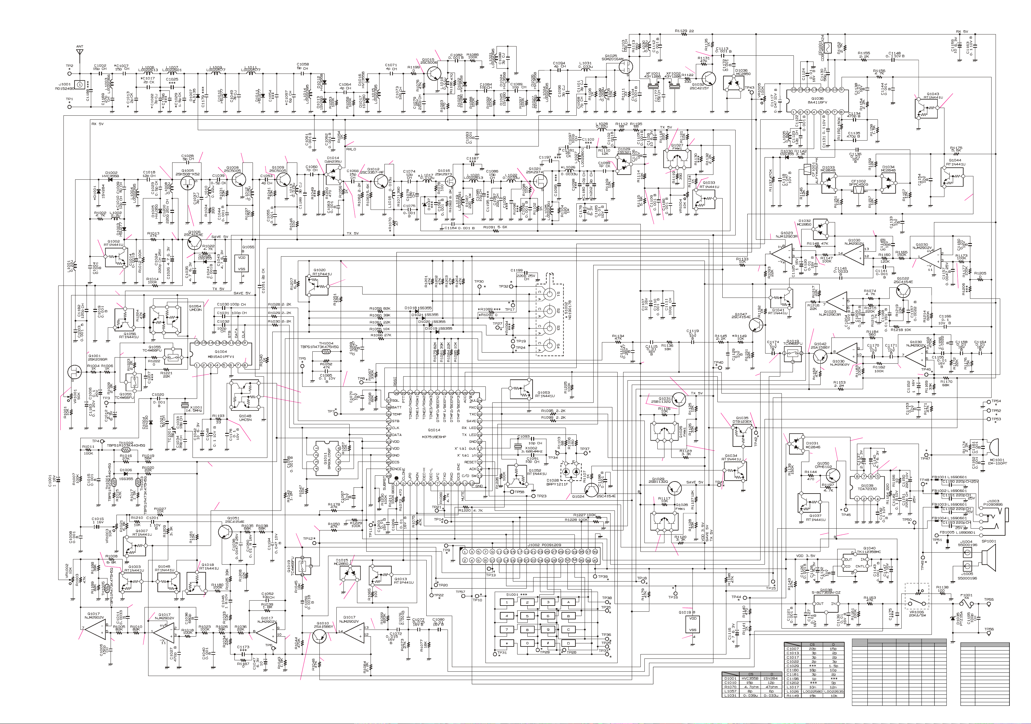
Circuit Diagram
MAIN Unit
RX: (4.81V)
TX: (0V)
RX: (4.18V)
TX: 4.21V
RX: (0.02V)
TX: (4.17V)
RX: (4.16V)
RX: (1.17V)
TX: 1.17V
RX: (0V) TX: 0V
RX: (0.78V)
TX: (0.6V)
RX: (4.88V)
RX: (3.74V)
TX: 3.76V
RX: (0.7V)
TX: 0.54V
RX: (4.06V)
TX: 4.08V
RX: 1.37V(1.37V)
TX: 1.43V
RX: 2.2V(2.2V)
TX: 0V
RX: 0V(0V)
TX: 0.69V
RX: 0V(0V)
TX: 2.26V
RX: 2.62 (2.62V)
RX: 0.75V (0.75V)
RX: 0V(0V)
TX: 5.01V
7.58V
TX HIGH: 2.6V
LOW: 1.23V
TX: (0V) [0V]
TX: (-1.25V)
[-0.9V]
RX: 1.8V (1.8V)
TX: 0V [0V]
RX: 0.72V (0.72V)
TX: 0V [0V]
TX:
(4.81V)
[2.8V]
TX: (1.95V)
[0.38V]
TX: (2.59V)[0.96V]
TX: (2.40V)[0.95V]
TX: (3.79V)[4.73V]
TX: (2.44V)
[0.68V]
TX: (3.96V)
[0.03V]
RX: 0.92V (0.92V)
RX: 4.86V
(4.86V)
RX: (0.93V)
RX: (0V)
RX: “3.58V” <0.02V>
RX: “0V” <3.57V>
RX: 2.07V (2.07V)
TX: {2.05V} <2.05V>
RX: 2.44V (2.44V)
TX: {2.44V} <2.44V>
RX: (0V)
TX: (0V)
RX: 4.88V (4.88V)
TX: 4.94V
RX: 0V (0V)
TX: 4.82V
RX: 4.86V (4.86V)
TX: 0V
RX: (4.81V)
RX: 4.85V (4.85V)
TX: (5.00V) [5.00V] {4.92V} <4.92V>
RX: 0V
(0V)
RX: 3.22V
(3.22V)
TX: 3.22V
RX: 3.52V (3.52V)
TX: (3.52V) [3.52V]
{3.52V} <3.52V>
RX: 0V (0V) [0V] {3.48V}
TX: (0V) [0V] {3.48V} <3.48V>
RX: 2.19V
(2.19V)
TX: 2.19V
RX: 3.44V (3.44V)
TX: (3.44V) [3.44V]
{3.44V} <3.44V>
RX: 3.50V (3.50V)
TX: 3.50V
RX: 4.88V (4.88V)
TX: 4.93V
RX: 3.52V (3.52V)
TX: (3.52V) [3.52V]
RX: 0V (0V)
TX: (3.52V) [3.52V]
RX: 3.20V (3.20V)
TX: 3.20V
RX: 3.12V(2.94V)
TX: (2.83V) [2.84V]
RX: (7.68V)
TX: (6.8V)[7.38V]
RX: (0V)
TX: (4.86V)[4.86V]
RX: (7.67V)
TX: (6.12V)[6.69V]
7.13V
RX: (3.51V) TX: 2.93V
TX: 7.2V
RX: (4.89V)
TX: 4.91V
RX: (3.52V)
TX: 3.52V
RX: (3.52V)
TX: 0V
RX: 1.82V (1.82V)
RX: (1.53V)
RX: (3.51V)
RX: (4.82V)
TX: 0V
RX: (0.04V)
TX: 4.91V
RX: 1.23V (0.58V)
RX: (1.53V)
RX: 7.69V
(0.21V)
RX: 7.69V
(6.91V)
RX: 0.9V (0.9V)
RX: (1.55V)
RX: (0.97V)
RX: (1.55V)
RX: 0V [7.66V]
RX: 0V (0V)
RX: (0.92V)
RX: (1.55V)
RX: (1.56V)
RX: 0V (1.25V)
RX: 0V (3.59V)
RX: (0.9V)
RX: [0V] {0V}
TX: (0.2V) [0.2V]
{0V} <0V>
TX: 2.2V
RX Squelch Close : xx TX : xx
RX Squelch Close W :[xx] TX High W : (xx)
RX Squelch Close N :{xx} TX Low W : [xx]
RX Squelch Open : (xx) TX High N : {xx}
RX Squelch Open W : “xx” TX Low N : <xx>
RX Squelch Open N : <xx>
TX: 2.17V
TX: 2.2V
TX: 2.2V
TX: 4.86V
RX: [3.0V] {0V}
”3.0V” <0V>
TX: (3.0V) [3.0V]
{0V} <0V>
RX: [0V] {3.47V}
”0V” <3.47V>
TX: (0V) [0V]
{3.47V}
<3.47V>
TX: 2.18V
RX: (3.51V)
RX: (0V)
RX: (0V)
TX: 2.22V
RX: 0V (0V)
TX: (2.17V) [2.17V]
{2.17V} <2.17V>
RX: 0V
TX: 0V
RX: 3.51V
TX: 3.52V (3.52V)
TX: 2.18V
RX: 0V (0V)
TX: (2.17V) [2.17V]
{2.17V} <2.17V>
RX: 0V (0V)
TX: (1.59V) [1.59V]
{1.59V} <1.59V>
RX: (3.51V)
TX: 2.22V
RX: (3.51V)
RX: (3.57V)
TX: 3.59V
RX: (3.52V)
RX: (0V)
RX: (3.52V)
TX: 3.52V
RX: 0V (3.51V)
RX: 7.69V (7.69V)
RX SQUELCH TX-W TX-N
Q1036
CLOSE OPEN HIGH LOW HIGH LOW
1 - - - - - 2 - - - - - 3 4.87V 4.87V 4.9V 4.9V 4.9V 4.9V
4 3.22V 3.22V 3.22V 3.22V 3.22V 3.22V
5 2.07V 2.07V 2.11V 2.12V 2.15V 2.15V
6 - - 0V 0V - 7 3.22V 3.22V 3.22V 3.22V 3.21V 3.21V
8 2.18V 2.18V 2.19V 2.19V 2.2V 2.2V
9 - - - - - -
10 - - - - - 11 - - - - - 12 - - - - - 13 - - - - - 14 - - - - - 15 - - - - - 16 - - - - - -
Q1036 (RX SQUELCH OPEN)
1 4.78V
2 4.4V
3 3.57V
4 4.8V
5 4.37V
6 4.5V
7 0.8V
8 0.6V
9 1.06V
10 4.81V
11 3.97V
12 0.47V
13 0.32V
14 1.91V
15 0V
16 0.93V
13
 Loading...