

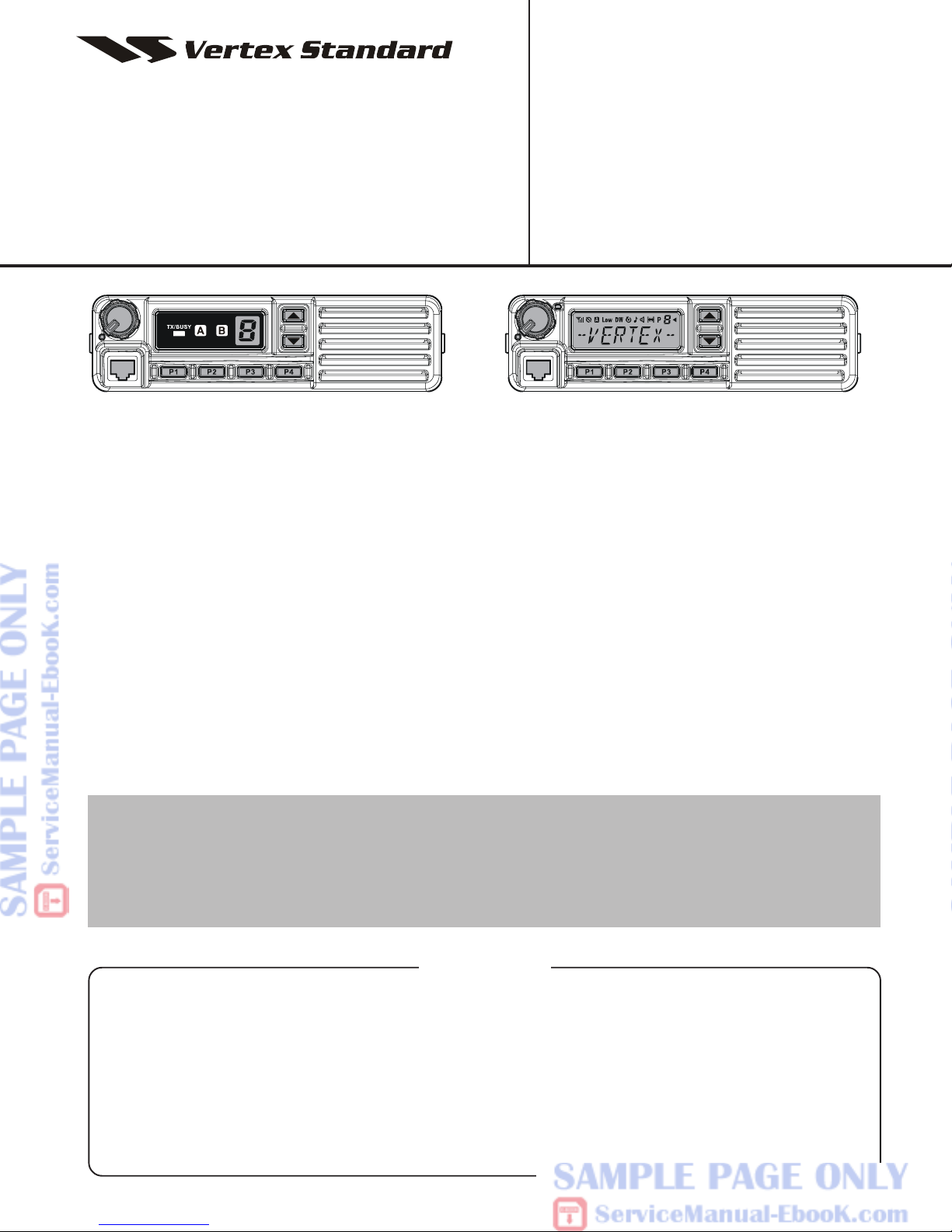
UHF FM Transceiver
VX-2100
VX-2200
Series
Series
Service Manual
2007 VERTEX STANDARD CO., LTD. EC061U90B
©
VERTEX STANDARD CO., LTD.
4-8-8 Nakameguro, Meguro-Ku, Tokyo 153-8644, Japan
VERTEX STANDARD
US Headquarters
10900 Wa ker Street, Cypress, CA 90630, U.S.A.
YAESU EUROPE B.V.
P.O. Box 75525, 1118 ZN Schiphol, The Netherlands
YAESU UK LTD.
Unit 12, Sun Valley Business Park, Winnall Close
Winchester, Hampshire, SO23 0LB, U.K.
VERTEX STANDARD HK LTD.
Unit 5, 20/F., Seaview Centre, 139-141 Hoi Bun Road,
Kwun Tong, Kowloon, Hong Kong
VX-2100
Series
VX-2200
Series
Introduction
This manual provides the technical information necessary for servicing the VX-2100/-2200 Series Mobile Transceiver.
Servicing this equipment requires expertise in handing surface-mount chip components. Attempts by non-qualified
persons to service this equipment may result in permanent damage not covered by the warranty, and may be illegal
in some countries.
Two PCB layout diagrams are provided for each double-sided board in this transceiver. Each side of the board is
referred to by the type of the majority of components installed on that side (“Side A” or “Side B”). In most cases one
side has only chip components (surface-mount devices), and the other has either a mixture of both chip and leaded
components (trimmers, coils, electrolytic capacitors, ICs, etc.), or leaded components only.
As described in the pages to follow, the advanced microprocessor design of the VX-2100/-2200 allows a complete
alignment of this transceiver to be performed without opening the case of the radio; all adjustments can be performed
from the personal computer, using with the Vertex Standard VPL-1 Programming Cable and CE82 Software.
While we believe the information in this manual to be correct, Vertex Standard assumes no liability for damage that
may occur as a result of typographical or other errors that may be present. Your cooperation in pointing out any
inconsistencies in the technical information would be appreciated.
Important Note
This transceiver was assembled using Pb (lead) free solder, based on the RoHS specification.
Only lead-free solder (Alloy Composition: Sn-3.0Ag-0.5Cu) should be used for repairs performed on this apparatus. The solder stated above utilizes the alloy composition required for compliance with the lead-free
specification, and any solder with the above alloy composition may be used.
Specifications ........................................................... A-1
DSUB 15-pin Accessory Connector ...................... B-1
Exploded View & Miscellaneous Parts ............... C-1
Block Diagram ......................................................... D-1
Circuit Description .................................................. E-1
Alignment ................................................................. F-1
Installation of Option ............................................ G-1
Contents
Board Units (Schematics, Layouts & Parts)
MAIN Unit .......................................................... H-1
FRONT-A Unit (VX-2100)................................... I-1
FRONT-B Unit (VX-2200)................................... J-1
Optional Units (Schematics, Layouts & Parts)
FVP-25 Encryption/DTMF Pager Unit ............. K-1
FVP-36
Voice Inversion Type Encryption Unit .....
L-1

Specifications
General
Frequency Ranges: 400 - 470 MHz (Type A)
450 - 512 MHz (VTX, Type D)
450 - 520 MHz (EXP, Type D)
350 - 390 MHz (Type I)
Number of Groups: 1 groups (VX-2100 Series)
8 groups (VX-2200 Series)
Number of Channels: 8 channels (VX-2100 Series)
128 channels (VX-2200 Series)
Power Supply Voltage: 13.6 V ± 15%
Channel Spacing: 12.5 / 25 kHz
Current Consumption (Approx.): TX: 11 A (45 W) or 6 A (25 W),
RX: 2.5 A,
Standby: 250 mA
Operating Temperature Range: –22 °F to +140 °F (–30 °C to +60 °C)
Frequency Stability: Better than ±2.5 ppm
RF Input-Output Impedance: 50 Ω
Dimension (W x H x D): 6.5” x 1.8” x 6.1” inch (165 x 46 x 155 mm) (W/O knob)
Weight (Approx.): 2.87 lbs (1.3 kg)
Receiver (Measured by TIA/EIA-603-A)
Sensitivity (12 dB SINAD): 0.25 μV
Intermediate Frequency: 1st: 67.65 MHz, 2nd: 450 kHz
Adjacent Channel Selectivity: 73 dB (25 kHz)
65 dB (12.5 kHz)
Intermodulation: 73 dB (25 kHz)
70 dB (12.5 kHz)
Spurious & Image Rejection: 80 dB
Audio Output: Internal: 4 W @18 Ω, 5% THD
External: 12 W @4 Ω, 5% THD
Transmitter (Measured by TIA/EIA-603-A)
Output Power : 45 / 25 / 10 W (50 W)
25 / 12.5 / 5 / 1 W (25 W)
Modulation: 16K0F3E,11K0F3E
Maximum Deviation: ±5 kHz (25 kHz)
±2.5 kHz (12.5 kHz)
Audio Distortion: < 3 % (@1 kHz)
Conducted Spurious Emission: 70 dB below carrier
Specifications subject to change without notice or obligation.
A-1
 Loading...