

UHF FM Transceiver
VX-160U/-180U
Service Manual
©2007 VERTEX STANDARD CO., LTD. EC013U90C
VERTEX STANDARD CO., LTD.
4 8 8 Nakameguro, Meguro Ku, Tokyo 153 8644, Japan
VERTEX STANDARD
US Headquarters
10900 Walker Street, Cypress, CA 90630, U.S.A.
YAESU EUROPE B.V.
P.O. Box 75525, 1118 ZN Schiphol, The Netherlands
YAESU UK LTD.
Unit 12, Sun Valley Business Park, Winnall Close
Winchester, Hampshire, SO23 0LB, U.K.
VERTEX STANDARD HK LTD.
Unit 5, 20/F., Seaview Centre, 139 141 Hoi Bun Road,
Kwun Tong, Kowloon, Hong Kong
VERTEX STANDARD (AUSTRALIA) PTY., LTD.
Normanby Business Park, Unit 14/45 Normanby Road
Notting Hill 3168, Victoria, Australia
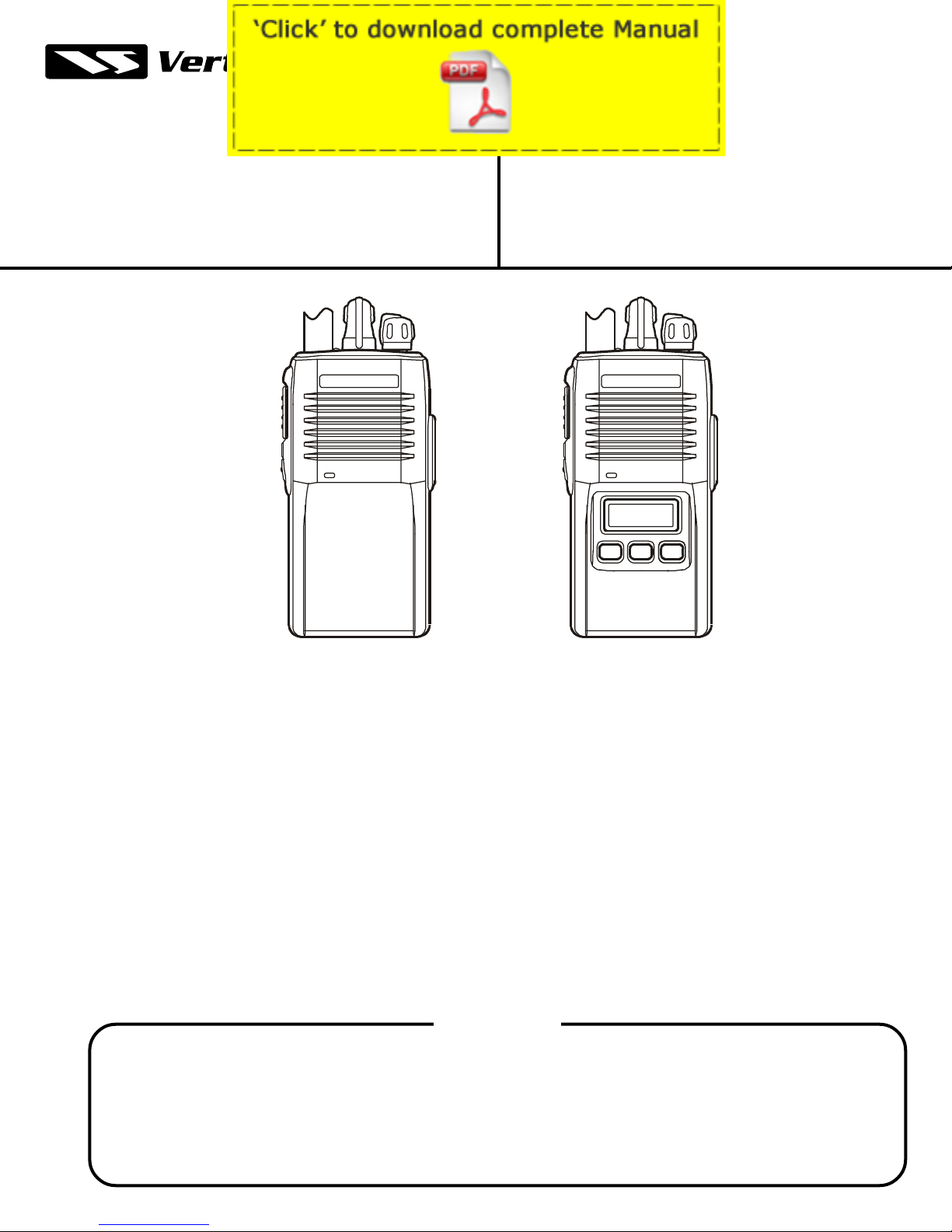
VX-160U VX-180U
Introduction
This manual provides technical information necessary for servicing the VX-160U and VX-180U FM Transceiver.
Servicing this equipment requires expertise in handling surface-mount chip components. Attempts by non-qualified
persons to service this equipment may result in permanent damage not covered by the warranty, and may be illegal in
some countries.
Two PCB layout diagrams are provided for each double-sided circuit board in the transceiver. Each side of is referred
to by the type of the majority of components installed on that side (“leaded” or “chip-only”). In most cases one side has
only chip components, and the other has either a mixture of both chip and leaded components (trimmers, coils, electrolytic
capacitors, ICs, etc.), or leaded components only.
While we believe the technical information in this manual to be correct, VERTEX STANDARD assumes no liability
for damage that may occur as a result of typographical or other errors that may be present. Your cooperation in pointing
out any inconsistencies in the technical information would be appreciated.
Contents
Operating Manual Reprint............................ 2
Cloning ........................................................................
6
Specifications ................................................... 7
Exploded View & Miscellaneous Parts ...... 8
Block Diagram ................................................. 9
Circuit Description ................................11
Alignment .................................................13
Board Unit (
MAIN Unit ............................................................... 17
Schematics, Layouts & Parts
)

GENERAL Specifications
Frequency Range (MHz): 400 - 430 (AS1)
450 - 485 (D)
485 - 512 (F)
Number of Channels: 16 channels
Channel Spacing: 12.5 / 25 kHz
PLL Steps 5 / 6.25 kHz
Power Supply voltage: 7.5 VDC ± 20%
Operating Temperature Range: –22°F to +140°F (–30°C to +60°C)
Frequency Stability: ±2.5 ppm
Dimensions (WHD): 2.3" (W) x 4.7" (H) x 1.2" (D) (58 x 120 x 31 mm)
Weight (approx.): 0.81 lb. (365 g) w/FNB-64
Specifications
RECEIVER Specifications (Measurements made per EIA standard TIA/EIA-603)
Sensitivity
EIA 12 dB SINAD : 0.25 µV
20 dB Quieting : 0.35 µV
Adjacent channel selectivity: 65 dB (25 kHz) / 60 dB (12.5 kHz)
Intermodulation: 65 dB
Spurious and Image Rejection: 65 dB
Hum & Noise 45 dB
Audio output: 500 mW @4 Ohms, 5% THD
service-repairmanual.com
TRANSMITTER Specifications (Measurements made per EIA standard TIA/EIA-603)
Power output: 5.0 / 1.0 W
Modulation: 16K0F3E, 11K0F3E
Conducted Spurious Emissions: 60 dB Below Carrier
FM Hum & Noise: 40 dB (25 kHz) / 35 dB (12.5 kHz)
Audio distortion (@ 1 kHz): < 5 %
Measurements per EIA standards unless noted above. Specifications subject to change without notice or obligation.
7
 Loading...