

Page 1
FORCE
4
SERVICE
MANUAL
110V
VALLEYLAB,
INC.
VALLEYLAB
5920
LONGBOW
303
EFFECTIVITY DATE: May
PART
530-2300
NUMBER
PRINTED
DRIVE,
P.O.
IN
A
USA
BOX
TWX
1,
1985
945
100
9015,
910-940-2514
054
A
BOULDER,
COLORADO
80301
Page 2

TABLE
OF
CONTENTS
SECTION
1.
INTRODUCTION
2.
INSTALLATION
3.
DESCRIPTION
4.
MONOPOLAR
CONFIGURATIONS
5.
TECHNICAL
6.
CIRCUIT
7.
TESTING
8.
TROUBLESHOOTING
9.
ASSEMBLIES
10.
PARTS
11.
WARRANTY
OF
AND
SPECIFICATIONS
DESCRIPTION
PROCEDURE
AND
LIST
CONTROLS
BIPOLAR
AND
ACCESSORIES
SCHEMATICS
&
INDICATORS
ELECTRO
SURGICAL
PAGE
1
2
4
13
15
21
43
50
76
116
135
Page 3
LIST
OF
ILLUSTRATIONS
FIGURE
1 FORCE 4
INDICATORS
AND OUTPUTS ON FRONT PANEL
2 FORCE 4 CONTROL KEYBOARD ON FRONT PANEL
3 FORCE 4 REAR PANEL CONTROLS AND CONNECTORS
4
5
6
7
8
9
10
11
12
13
14
15
16
17
18
19/20
21/22
23/24
25/26
27/28
29/30
31/32
33/34
35/36
37/38
39/40
41/42
43/44
45/46
47/48
49/50
51/52
OUTPUT
OUTPUT
OUTPUT
BLOCK
TIMING
BLOCK
OUTPUT
FORCE4BLOCK
MONOPOLAR
BIPOLAR
TROUBLESHOOTING
FORCE4COMPONENT/CONNECTOR
FORCE4COMPONENT/CONNECTOR
SYSTEM
PCB
CPU
OUTPUT
INTERFACE
BIPOLAR
BIPOLAR
CLOCK/CONTROL
SENSE
DRIVER
STRIPLINE
MONOPOLAR
BIPOLAR
POWER
POWER
VOLTAGE
DIAGRAM
VS
VS
-
LOAD
LOAD -
VS
BIPOLAR
WAVEFORMS -
DIAGRAM-CONTROL
POWER
SUPPLY
SCHEMATIC
OUTPUT
OUTPUT
INTERCONNECT
INTERCONNECT
BOARD
ASSEMBLY/SCHEMATIC
BOARD
BOARD
OUTPUT
WAVEFORMS
WAVEFORMS
WAVEFORMS
LIST
ASSEEMBLY/SCHEMATIC
ASSEMBLY/SCHEMATIC
BOARD
CONTROLLER
BOARD
BOARD
BOARD
ASSEMBLY/SCHEMATIC
ASSEMBLY/SCHEMATIC
BOARD
ASSEMBLY/SCHEMATIC
DISPLAY
DISPLAY
BOARD
- MONOPOLAR
BIPOLAR
CONTROL
SETTING
STAGE
CLOCK/CONTROL
MODULE
TIMING
DIAGRAM
LOCATIONS-TOP
LOCATIONS-SIDE
SCHEMATIC
ASSEMBLY/SCHEMATIC
BOARD
ASSEMBLY/SCHEMATIC
ASSEMBLY/SCHEMATIC
BOARD
ASSEMBLY/SCHEMATIC
ASSEMBLY/SCHEMATIC
SPEAKER BOARD ASSEMBLY/SCHEMATIC
POWER
POWER
MONOPOLAR
BIPOLAR
POWER
SUPPLY
SUPPLY
OUTPUT
BOARD
CONTROLLER BOARD ASSEMBLY/SCHEMATIC
KEYBOARD/SCHEMATIC
KEYBOARD/SCHEMATIC
SUPPLY
MODULE/SCHEMATIC
ASSEMBLY/SCHEMATIC
BOARD
VIEW
VIEW
PAGE
4
8
11
18
19
20
27
35
36
41
42
68
70
72
77
78
98
80
81
84
86
88
90
92
94
96
98
100
102
104
106
108
110
112
114
LIST
TABLE
OF
TABLES
INPUT
SIGNALS
&
OUTPUT
ON
CPU
LINES
BOARD
-
BIPOLAR
PAGE
CONTROL
11
29
32
Page 4
SECTION
INTRODUCTION
This
Service
the
Valleylab
sections
Testing
use
of
and
elect
directed
1
Manual
Model
covering
Troubleshooting
rosurgery
to
the
Operator's
covers
the
FORCE
Technical
is
beyond
Instruction
the
installation
4
Electrosurgical
Specifications,
of
the
Generator.
the
scope
Manual
and
basic
Generator.
of
this
provided
service
Circuit
Detailed
manual
by
instructions
Also
included
Descriptions
instructions
and
the
Valleylab.
and
in
reader
for
are
the
the
is
Valleylab,
in
equipment
obligation
and/or
sold
its
to
by
dealers
built
make
them.
and/or
the
and
representatives
sold
same
or
by
similar
them
reserve
at
changes
any
the
time
on
equipment
right
without
to
make
incurring
previously
changes
any
built
Page 5
SECTION
INSTALLATION
2
INSTALLING
The
compact
unit
convenient
At
is
may
high
important that the vents on the rear
proper
closely
air.
top
and
POWER FOR THE
90-140
The
FORCE4is
voltages
of
brownouts
constant.
(nominal).
PROPER
THE FORCE 4
size
of
the
FORCE
4 system allows a variety
be placed on the mounting cart
and
power
cooling.
fitting
Under
rear
VAC,
with
The
GROUNDING
sturdy
settings
cabinet or
continuous
panel
FORCE
50
essentially
or
FORCE4is
table
For
this
to
feel
4
-
60
Hz
designed
power
or
cart.
considerable
reason
cart
use
for
extended
warm
perfect
surges
to
operate
the output
normally
to
power
the
which
the
output
available
is
and
FORCE
might
periods
touch.
over
regulation.
of
supplied
of
installations.
from
Valleylab, or on any
dissipated within the unit
sides
4 should not be
restrict
of
an
unusually
the
for
remain
the
free
time,
FORCE4will
operation
it
is
wide
This means
unobstructed for
installed
circulation
normal
range
that
always remain
on
120
and
for
of
in
volts
The
it
in a
of
the
input
case
AC
An
important
equipment
connected
flow
failure.
Undesirable
the
assure
the
POWER
Unless
equipped
meets
by
be
from
input
proper
FORCE
PLUGS
an
all
using
periodically
consideration
is
proper
to
the
generator
the
cabinet
60
Hz
60 Hz
4.
FOR
explosion-proof
with
requirements
extension
power
grounding
THE
an
approved
disassembled
grounding.
leakage
to
FORCE
for
cords
chassis
of
the
and
4
hospital
safe
or
in
assuring
the
unit
currents
unit.
polarity
connector
grounding.
3-prong
and
inspected
The
and
are
duty
to
patient
ground wire
insures
in
the
also
It
is
the
in
the
power
is
specified,
three-prong
Its
2-prong
by
safety
that
no
event
affected
qualified
of
responsibility
outlets
connector.
purpose
adapters.
while
in
the
dangerous
an
internal
by
the
the
110
should
The
maintenance
using
power
currents
polarization
of
furnishing
volt
This
not
connector
electrical
cable
electrical
the
user
power
FORCE
connector
be
defeated
should
personnel.
will
4
is
of
to
to
is
Page 6
220
volt
volt
tandem
Hospital
volt
connectors
country
room.
connectors
AC
Grade
will
versions
blade
110
and
used
in
equip your
of
the
FORCE4are
connector
volt
connector. At present there are no Hospital
we do
other
FORCE
of
equivalent
not
countries.
4 with
have
access
The
the
shipped
quality
Valleylab
proper
with
and
to
all
connector
a
the
representative
standard
construction
various
for
your
U.S.A.
to
Grade
220
in
operating
220
the
220
volt
your
ROUTINE
The
Maintenance
repairing
the
replacement
PULL
We
year.
MAINTENANCE
solid-state
cords
cord
ON
recommend
it
THE
This
design
is
limited
and
should
problems.
CORD
ITSELF.
that
Service
AND
replacing
the
Manual
procedures. For major
your
Valleylab
information
representative.
needed
to
INSPECTIONS
of
the
to
periodic
be
replaced.
Cords should
FORCE4be
describes
repairs
repair
the
FORCE4assures
inspections.
accessories.
Proper
handling
always
inspected
the
recommended
the
If
desired,
FORCE
FORCE
4 can be returned
4.
virtually
Repair
Should
be
grasped
by
the
Valleylab
maintenance-free
should
breakage
will
hospital
minimize
by
the
inspection
will
supply
be
limited
or
wear
repair
plugs.
engineer
and check-out
to
Valleylab or
any
occur
DO
twice
parts
use.
to
to
and
NOT
a
or
Page 7
SECTION
3
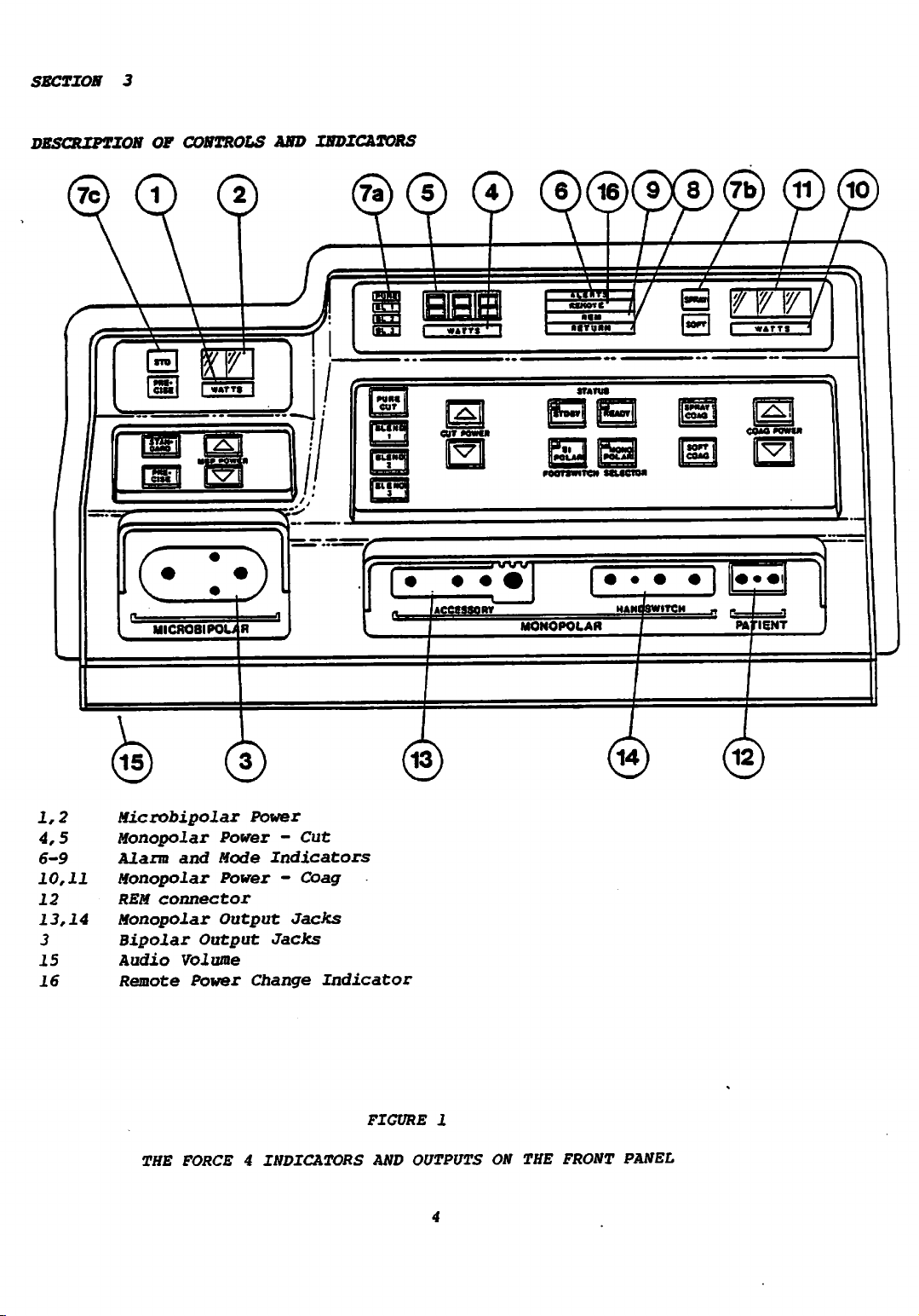
DESCRIPTION
OF CONTROLS AND
MICR08IPOU
R
INDICATORS
• • •
ACCCSSORT
iTVW
6)(16H9Y8)(7b)
mrumi
MONOPOLAR
< \torr\ I
ITCH
(11)
wtts
(10
1
^!
com
rawcii
s2
2
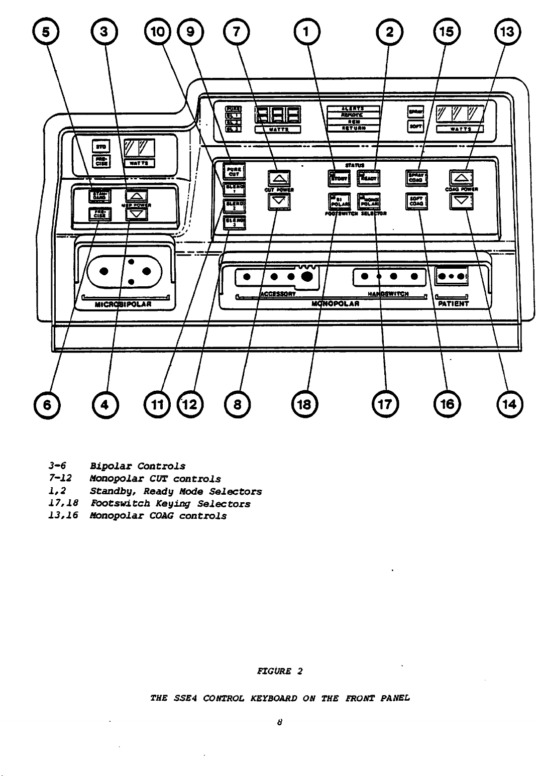
1,2
4,5
6-9
10,11
12
13,14
3
15
16
Microbipolar
Monopolar
Alarm
and
Monopolar
REM
connector
Monopolar
Bipolar
Audio
Remote
THE
Output
Volume
Power
FORCE4INDICATORS
Power
Power-Cut
Mode
Power
Output
Indicators
-
Coag
Jacks
Jacks
Change
Indicator
FIGURE
AND
1
OUTPUTS
ON THE
FRONT
PANEL
Page 8

A.
FRONT PANEL
1.
BIPOLAR
The
at
generator
2.
BIPOLAR
OUTPUT
word
the
Microbipolar
POWER
INDICATORS
ACTIVE
'WATTS'
is
keyed
READOUT
AND OUTPUTS
INDICATOR
will
be
Output Jack
in
the
illuminated
bipolar
(SEE
(3).
mode
when
may
FIG.
useful
Absence
indicate
1)
output
of
illumination
generator
power
is
available
when
the
malfunction.
This
mode
power,
generator
3.
BIPOLAR
This
will
accessories
when
4.
MONOPOLAR
The
the
monopolar
generator
5.
MONOPOLAR
This
mode
cut
generator
digital
(2,
Fig.
in
watts,
is
ACTIVE
receptacle
be
keyed
the
bipolar
CUT
backlit
cut
mode
output
is
CUT
digital
(2,
Fig.
power,
is
LED
2).
keyed
RECEPTACLE
will
by
and
OUTPUT
word
and
keyed
POWER
LED
2).
in
watts,
keyed
display
The number
which
in
the
accept
the
the
bipolar
foot
switch
ACTIVE
'WATTS'
useful
jacks
indicates
READOUT
display
The number
in
is
visible
will
bipolar
the
handswitch.
generator
button,
INDICATOR
will
output
(13) and
a
is
which
the
will
monopolar
when
displayed
be
delivered
mode.
three
prong
It
(18,
be
visible
power
(14).
malfunction.
visible
displayed
be
delivered
cut
will
is
Absence
when
mode.
the
predicts
to a 100
active
also
then
Fig.
when
is
available
the
predicts
generator
bipolar
accept
keyed
2),
is
the
generator
of
illumination
generator
the
to
a 300
the
level
ohm
two
by
pressed.
at
level
ohm
is
in
the
of
load
when
accessories
prong
the
foot
is
either
is
in
the
of
monopolar
load
ready
bipolar
active
switch
keyed
of
when
ready
when
the
and
in
the
the
the
6.
7.
ALERT
This
condition.
MODE
A.
INDICATOR
One
waveform.
selector
INDICATOR
LED
lamp
of
four
is
on
The
audio
LAMPS
CUT
mode
The mode may
push
buttons
whenever
alarm
indicators
(9,10,11,12;
will
be
the
sound
is
changed
generator
twice
illuminated
by
pressing
Fig.
2)
when
is
this
disabled
lamp
to
show
one
of
goes
the
the
by
on.
CUT
four
an
alarm
power
mode
Page 9
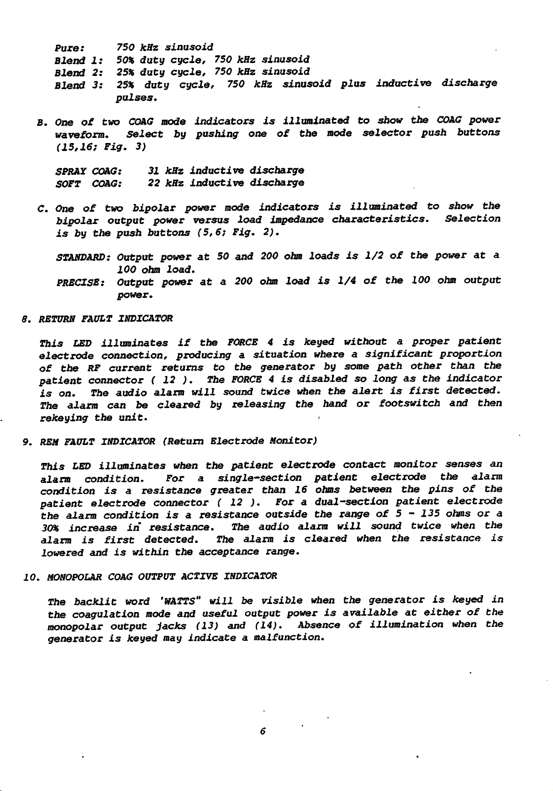
Pure: 750 kHz
Blend
Blend
Blend
1:
2:
3:
50%
duty cycle,
25%
duty
25%
duty
pulses.
sinusoid
cycle,
cycle,
750
kHz
750
kHz
750 kHz
sinusoid j
sinusoid
sinusoid
plus
inductive
discharge
B. One
C. One
8.
RETURN
This
electrode
of
patient
is
The
rekeying
of
two
waveform.
(15,16;
SPRAY COAG:
SOFT
bipolar
is
STANDARD:
COAG:
of
by the
Fig.
two
output
PRECISE:
FAULT
LED
illuminates
connection, producing a
the
RF
current
connector ( 12
on.
alarm
The
can
the
COAG
Select
mode
by
indicators
pushing
is
one
3)
31
kHz
inductive
22
kHz
inductive
bipolar
power
push
buttons (5,6;
Output
100
ohm
Output power
power.
INDICATOR
audio
alarm
power
versus
power
at
50 and 200
load. j
at
if
the
returns
).
to
The
will
be cleared by releasing the
unit.
discharge
discharge j
mode
a 200
indicators
load
Fig.
2). j
ohm
FORCE4is
situation
the
generator
FORCE4is
sound
twice
illuminated
of
the
impedance
ohm
loads
load
keyed without a proper patient ^
where
disabled
when
to
show
mode
is
selector
illuminated
characteristics.
is
1/2
is
1/4
of
a
significant
by
some
path
so long
the
alert is first
hand
•
or footswitch
of
the
the
the
100
other
as
COAG
push
to
buttons
show
power
the
Selection
power
ohm
at
output
a
proportion j
the
than
indicator
the
detected.
and
then J
9.
REM
FAULT
This
alarm
condition
patient
the
alarm
30%
increase in resistance.
alarm
lowered
10.
MONOPOLAR
The
the
coagulation
monopolar
generator
INDICATOR
LED
illuminates
condition.
is
electrode
condition
is
first
and
COAG
backlit
output
is
is
a
within
word
keyed
(Return
when
For
a single-section patient electrode the
resistance
connector ( 12
is
a
resistance
detected.
the
acceptance
OUTPUT
mode and
ACTIVE
'WATTS"
jacks
may
useful
(13) and
indicate
Electrode
the
patient
greater
).
The
The
alarm
INDICATOR
will
be
output
a
Monitor)
electrode
than 16
For a
outside
audio
range.
visible
(14).
malfunction.
alarm
is
power
Absence
cleared
when
contact
ohms
between the
dual-section
the
range
will
the
is
available
of
sound
when
generator
of
illumination
monitor
patient
5 -
135
twice
the
resistance
at
senses
pins
ohms
is
either
an
alarm
of
the J
electrode
or
when
keyed
when
the j
is
of
the
the
a ^
in
Page 10
12.
MONOPOLAR
COAGULATION
POWER READOUT
This
coagulation
when
PATIENT
This
monopolar
actuates
section
13.
MONOPOLAR
This
(Valleylab
output
button
14.
MONOPOLAR
accessories.
have
mode
digital
(2,
Fig.
the
generator
RETURN
2
pin
a
patient
ACTIVE
receptacle
can
(17,
or
coagulation
ACTIVE
receptacle
no
power
or
coagulation
LED
display
2).
power,
is
The
in
keyed
ELECTRODE
receptacle
procedures.
switch
electrode
accepts
within
RECEPTACLE-HAND
will
LectroSwitch)
be
activated
Fig.
This
available
accept
2)
is
mode power may be
RECEPTACLE - HANDSWITCH
will
output
mode
is
visible
number
watts,
in
displayed
which
the
RECEPTACLE
the
A
pin
the
receptacle
used
or
by
pressed
accept
if
power
for
three-prong
standard
the
is
activated
the
generator
may
when
will
monopolar
patient
on
contact
OR
FOOTSWITCH
one-prong
footswitch
or
by
keyed
the
be
keyed
three-prong
the
generator
predicts
be
delivered
coagulation
return
the
patient
to
indicate
area
(REM)
handswitching
active
when
the
handswitching
at
this
only
is
by
keyed
at
this
the
level
electrode
electrode
the
monitoring.
active
accessories.
the
monopolar
receptacle.
handswitching
the
handswitch
by
the
receptacle.
is
to
a
mode.
connector
use
accessory.
footswitch.
in
the
of
monopolar
300
ohm
connector
of
the
accessories
footswitch
and
ready
load
used
dual-
This
Cut
active
will
Cut
15.
16.
AUDIO
The
keyed
forward
volume
REMOTE
This
remote
When
off
VOLUME
volume
may
of
INDICATOR
lamp
power
the
by
switching
to
lamp
CONTROL
of
be
adjusted
increase
the
will
change
the
'bong'
be
is
to
cut
and
with
the
produced
illuminated
feature
on,
remote
standby
coag
this
volume,
(1,
audio
by
is
power
Fig.
tones
4-position
push
and
activated
it
alarm
the
changes
3).
produced
slide
back
conditions
audio
at
can
switch.
to
decrease
is
will
the
handswitching
occur.
when
not
'bong'
The
the
generator
Pull
the
volume.
adjustable.
once
lamp
the
switch
when
accessory.
is
turned
is
The
the
Page 11
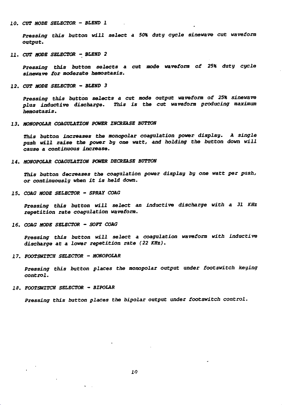
3-6
7-12
1,2
17,18
13,16
Bipolar
Monopolar
Standby,
Footswitch
Monopolar
Controls
CUT
Ready
Keying
COAG
controls
Mode
Selectors
controls
Selectors
THE
SSE4
CONTROL
FIGURE
KEYBOARD
8
2
ON
THE
FRONT
PANEL
Page 12

B.
FRONT PANEL KEYBOARD CONTROLS
1.
STANDBY
In
suppressed.
be
2.
READY
this
blank.
MODE
MODE
mode
SELECTOR
the
Prior
The
generator
SELECTOR
generator
power
level
is
(SEE
cannot
in
FIGURE
settings
standby
be
when
2)
keyed
are
and
retained
power
is
the
but
first
audio
the
displays
applied.
alerts
are
will
3.
4.
5.
6.
7.
Pressing
alarms
BIPOLAR
push,
fully
This
button
the
power by one
the
display
BIPOLAR
Pressing
or
STANDARD
Pressing
PRECISE
Pressing
MONOPOLAR
This
button
increase
the
display
this
POWER
button
active.
INCREASE
increases
to
increase
POWER
this
DECREASE
button
continuously
MODE
MODE
this
this
CUT
SELECTOR
button
SELECTOR
button
POWER
increases
the
power
to
the
the
watt.
decreases
if
will
will
INCREASE
by
mode
places
BUTTON
bipolar
Holding
continuously
BUTTON
the
button
select
select
BUTTON
the
monopolar
one
watt,
maximum.
the
the
generator
power
the
to
bipolar
is
the
Standard
the
Precise
cut
and
holding
readout.
button
70
watts
held
power
in
down
power
down.
Bipolar
Bipolar
readout.
the
service
A
single
continuously
maximum.
display
mode.
mode.
button
with
by
A
single
down
push
will
outputs
will
will
one
watt
push
and
raise
cause
per
will
increase
8.
MONOPOLAR
Pressing
watt
9.
CUT
Pressing
per
MODE
CUT
POWER
this
button
push,
SELECTOR
this
button
DECREASE
or
continuously
-
PURE
will
decreases
CUT
select
BUTTON
the
if
a
monopolar
the
button
continuous
cut
mode
is
held
sinewave
power
down.
cut
display
waveform
by
one
output.
Page 13
10.
CUT
MODE
SELECTOR
- BLEND 1
11.
12.
Pressing
output.
CUT
MODE
Pressing
sinewave
CUT
MODE
this
SELECTOR-BLEND
for
SELECTOR - BLEND 3
button
this
moderate
button
will
2 j
selects
hemostasis.
select
a
Pressing this button selects a cut
plus
hemostasis.
13.
MONOPOLAR
This
push
cause
14.
MONOPOLAR COAGULATION POWER DECREASE BUTTON
This
or
inductive
COAGULATION
button
will raise
a
continuous
button
continuously
discharge.
increases
the
increase.
decreases
when
POWER
the
power
the
it
is
This
INCREASE BUTTON
monopolar
by
one
coagulation
held
down.
a
50%
duty
cut
mode waveform
mode
is
the
coagulation
watt,
and
power
cycle
output
cut
waveform producing
sinewave
waveform
power
holding
display
the
by
cut
waveform
of
25%
of
duty
25%
cycle
sinewave
maximum
display. A single ^
button
one
watt
down
per
will j
push,
15.
COAG MODE
Pressing
repetition
16.
COAG MODE
Pressing
discharge
17.
FOOTSWITCH
Pressing
control.
18.
FOOTSWITCH
Pressing
SELECTOR-SPRAY
this
SELECTOR
this
this
this
button
rate
coagulation
button
at a lower
SELECTOR
button
SELECTOR-BIPOLAR
button
will
-
SOFT
will
repetition
- MONOPOLAR
places
places
COAG
select
waveform.
COAG
select
the
the
an
a
rate
(22
monopolar
bipolar
inductive
coagulation
KHz).
output
output
under
discharge
waveform
under
footswitch
with
with
footswitch
control.
a 31
KHz
inductive
keying
10
Page 14
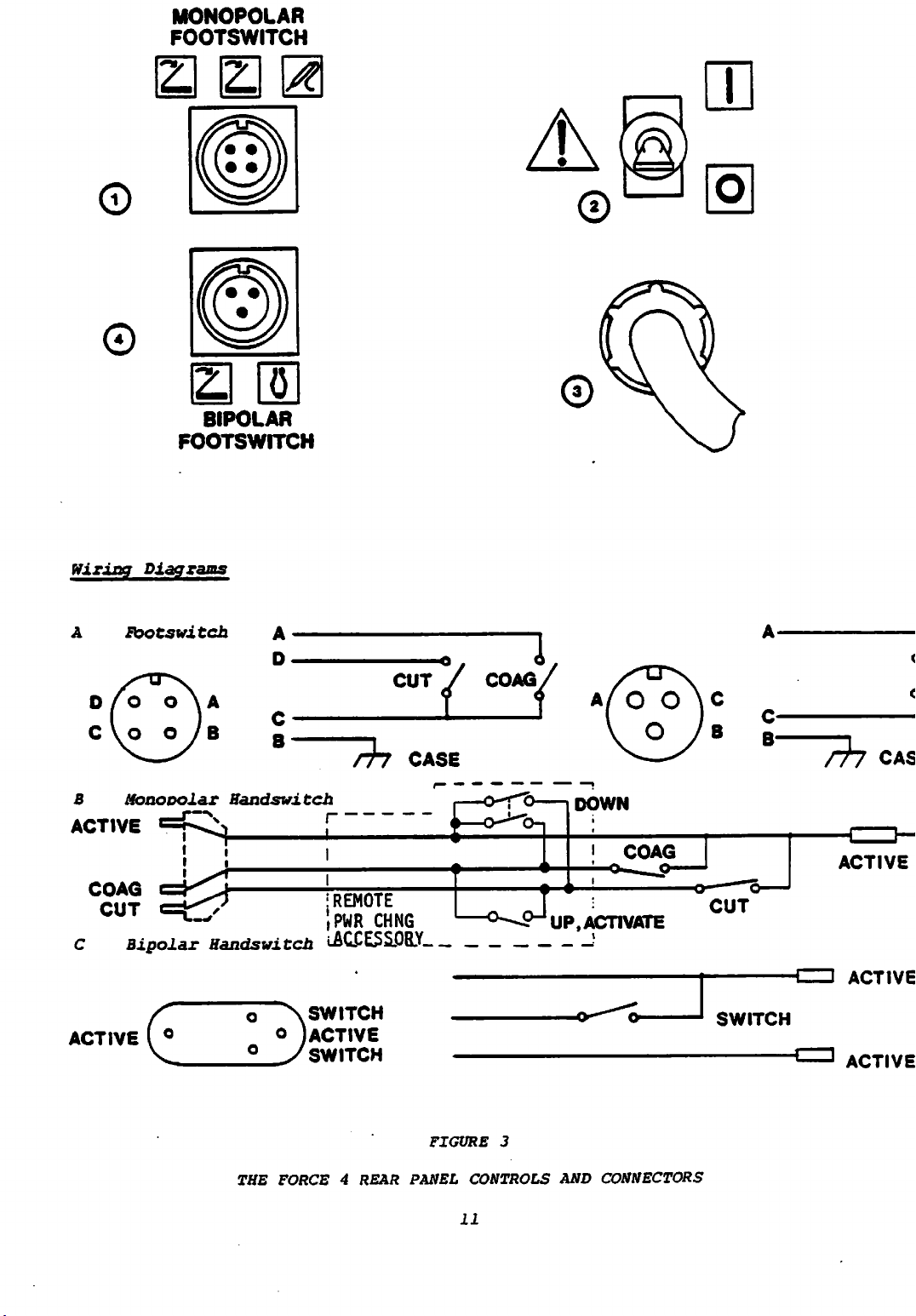
0
©
MONOPOLAR
FOOTSWITCH
21 21 A
BIPOLAR
FOOTSWITCH
Wiring
A
D
C
B
ACTIVE
COAG
footswitch
Ao
\o
Monopolar
cut
Diagrams
OU
OJ B
=*<>
=t^7
C Bipolar
ACTIVE
( °
A
D
C
B
Handswitch
^ r
i ;
JJandswitch
o
ASWITCH
O
° J
CUT
^7
;REMOTE
I
PUR
CHNG
L&C.CE5S.0B.Y
jACTIVE
SWITCH
/
f f
CASE
1
COAG/
O-i
O-l.m
UP.ACT1VATE
/^"CT*\
AfOOV
W
DOWN
i
COAG
!
in
B
CUT
SWITCH
B"
Th
ACTIVE
ACTIVE
1
CASE
ACTIVE
THE
FORCE4REAR
FIGURE
PANEL
3
CONTROLS
11
AND
CONNECTORS
Page 15
REAR
1.
FOOTSWITCH
PANEL
CONTROLS
AND CONNECTORS
RECEPTACLE-MONOPOLAR/BIPOLAR
(SEE
FIG.
3)
This
connector.
2.
POWER
This
apply
3.
POWER
The
connected
4.
FOOTSWITCH
This
connector.
4-pin
SWITCH
power
power
CORD
line
toaproperly
three-pin
The
switch
and
cord
MS-type
wiring
includes
down
is
receptacle
diagram
to
shut
terminated
phased,
RECEPTACLE-BIPOLAR
MS-type
receptacle
a
circuit
power
accepts
is
shown
off.
in
a
grounded
accepts
in
Fig.
breaker.
grounded
receptacle.
the
3.A.
Press
3-pin
the
single-treadle
two-treadle
the
toggle
plug
and
footswitch
upward
should
footswitch
to
be
12
Page 16
SECTION
4
MONOPOLAR
ELBCTROSURGICAL
&
ACCESSORIES
The
FORCE4features
these
HANDSWITCH
switching
switching
output
AND
outputs
pencil.
accessories
is
a
output
nonswitching
accessory
MONOPOLAR
Monopolar
The
or
CONFIGURATION
Accessories
FORCE
operation,
through
contacts
The
on
"active"
Models
the
the
Valleylab
either
E4001
the
since
receptacle.
most
footswitch
E6008
connected
back
generator
Bipolar
activated
4
switching
mixture
spark
standard
panel
has
and
to
in
only.
in
an
currents
of
energy
then
E6009
millijoule.
1/5000
operation.
of
the
BIPOLAR
CONFIGURATIONS
are
used
is
The
reduced
bipolar
by
4
has
the
the
radio
power
accessories
footswitch.
a
patient,
patient's
hand-switching
"Handswitch"
there
and
E4002
The
standard
accessories
controls
footswitches
the
FORCE4by
of
the
CUT/BLEND
The
FORCE4has
the
event
"intrinsically
are
flammable
which
The
energy
amount
three
separate
primarily
designed
MONOPOLAR
or
it
BIPOLAR
radio
frequency
frequency
and
returns
skin.
accessories
or
are
only
coagulation
active
directly
the
means
generator.
or
COAGasneeded.
that
gas
too
both
safe"
low
and
occurs
present
considered
in
for
ACCESSORY
can
be
output
and may he
current
to
"Accessory"
low,
"accessory"
current
are
The E6008
an
override
pedals
footswitch
to
oxygen.
at
the
in
a
outputs
monopolar
use
with
activated
which
(RF)
passes
the
generator
plug
switching
forceps
or
through
flow
designed
of
a
four-pin
circuit
are
cause
a
To
switch
the
FORCE4switching
conservative
which
configurations.
either
output
by
may
activated
grounded
from
into
receptacles.
voltages
also
jack
an
to
the
for
operating
footswitch
footswitch
The E6009
pushed
circuit.
spark
qualify
contacts
limit
may
be
activated.
switching
is
designed
the
footswitch.
be
used
by
either
output.
the
via
a
patient
the
three
All
between
plug
accessory.
into
will
appropriate
accept
pedals
activates
to
insure
simultaneously.
This
even
in
as
intrinsically
the
must be
for
safe,
The
forceps
for
with
switching
the
In
active
plate
banana
three
either
the
adapter.
Both
room
receptacle
use
activate
the
that
only
means
most
less
circuits
open-
Two
of
MONOPOLAR
or
a
use
with
The
third
or
switching
monopolar
accessory,
which
pin
jacks
pins
the
monopolar
plugs
the
and
on
are
pins.
of
The
Model
are
the
the
Force4in
COAG
is
The
FORCE
that
the
dangerous
safe,
the
than 1
is
about
contact
The
In
a
densities
Patient
monopolar
to
Return
configuration,
a
safe
Electrode
level.
a
return
electrode
13
is
used
to
limit
the
current
Page 17

An
accepted
square
per
A
delicate
inches.
as
adherance
method
system
centimeter
hundred
Gelled
Valleylab
of
with
procedure
to
providing
electrosurgical
ground. The
returning
safety
through
from
standard
watts
foam
of
return
of
generator
which
pad
for
gelled
electrode
output.
uses
electrodes,
low
plate
area
(NFPA
power
and
Model E7503, 5, 6, 7 have come
manufacturer's
a
return
current
circuit
ground
patient
burns
the
fault
prevents
instructions,
return
circuit
in
the
is
under
connection.
which
patient
FORCE4operation
excessive
common
fault
or
foil
or
Bulletin
settings
conductive
into
they
The
continuously
circuit
and
thus
conditions.
electrodes
roughly 9
No.
requires
adhesive
common
can
be
FORCE4is
and
the
if
the
provides
is
or
10 square
76CM,
only
electrodes
usage and
an
effective
monitors
power
proportion
a
high
1.5
watts
Part
a
few
with
an
RF
the
distribution
of
degree
inches
II.)
square
such
proper
and
safe
grounded
flow
current
per
of
of
BIPOLAR
Bipolar
The
connected
is
output
CONFIGURATION
Accessories
most
limited
operates
impedance
coagulation
power
when
common
to
to
the
the
bipolar
BIPOLAR
tissue
at
characteristics
at
a
given
the
coagulation
lower
instruments
output
which
power
optimized
power
is
complete.
jacks.
is
grasped
levels
setting
are
In
than
for
and an
forceps,
bipolar
by
the
the
operation
jaws.
MONOPOLAR
desiccation.
automatic
the
jaws
The
of
the
FORCE
output
This
means
reduction
which
current
4 BIPOLAR
and has
of
are
flow
faster
output
14
Page 18
SECTION
5
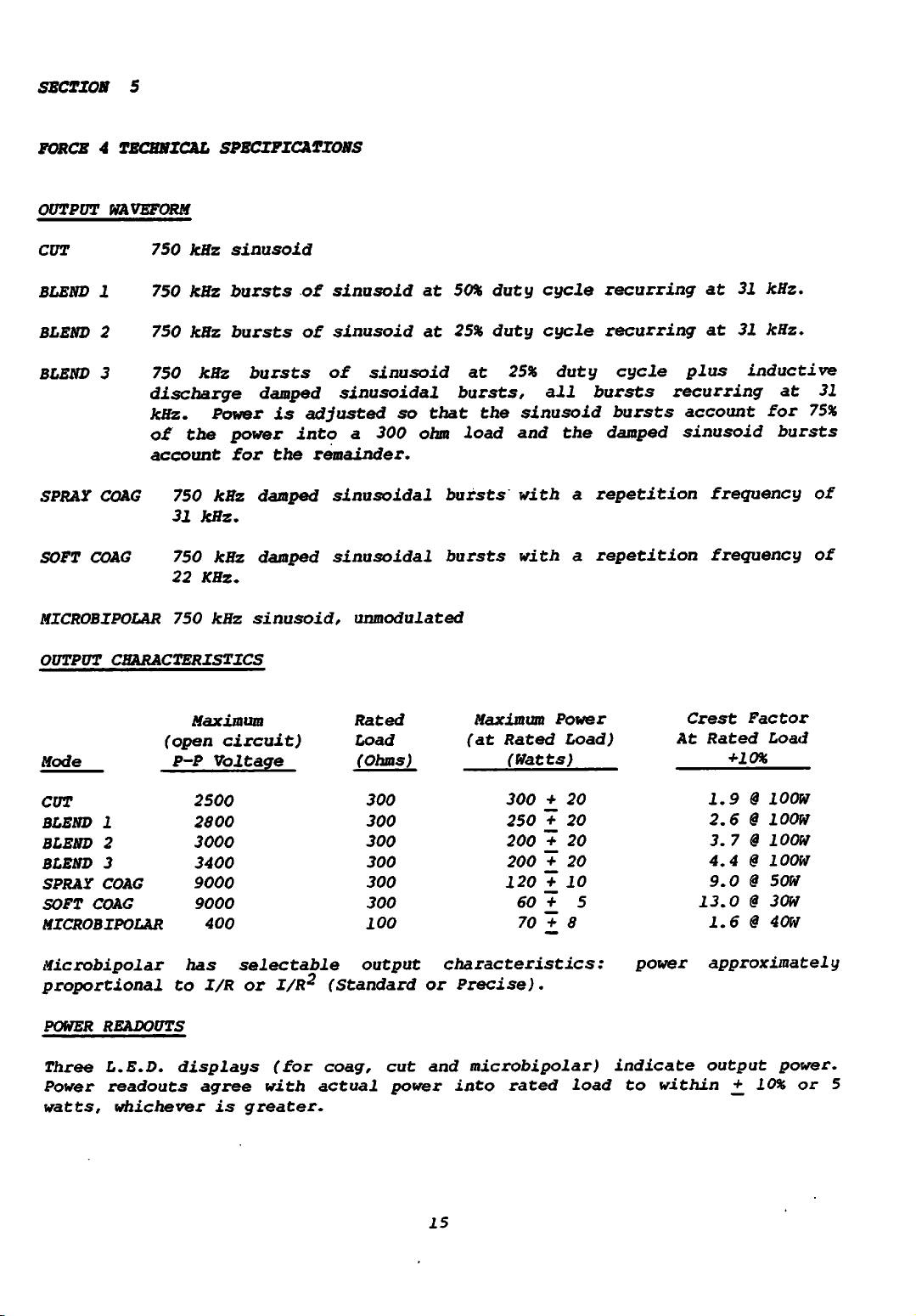
FORCE4TECHNICAL
OUTPUT
CUT
BLEND
BLEND
BLEND
WAVEFORM
750
1
2
750
750
3
750
discharge
kHz. Power
of
the
account
SPRAY
SOFT
MICROBIPOLAR
COAG
COAG
750 kHz damped
31
750 kHz damped
22
750
SPECIFICATIONS
kHz
sinusoid
kHz
bursts
kHz
bursts
kHz
bursts
damped
power
for
kHz.
KHz.
kHz
sinusoid,
is
into
the
of
sinusoid
of
sinusoid
of
sinusoidal
adjusted
a 300
remainder.
sinusoidal
sinusoidal
unmodulated
sinusoid
so
ohm
at
at
that
hursts
bursts
50%
duty
25%
duty
at
bursts,
the
load
cycle
cycle
25%
all
sinusoid
and
with a
with
duty
the
a
recurring
recurring
cycle
bursts
bursts
damped
repetition
repetition
at
31
at
31
plus
recurring
account
sinusoid
frequency
frequency
kHz.
kHz.
inductive
at
for
bursts
31
75%
of
of
OUTPUT
Mode
CUT
BLEND
BLEND
BLEND
SPRAY
SOFT
MICROBIPOLAR
Microbipolar
CHARACTERISTICS
(open
P-P
1
2
3
COAG
COAG
has
Maximum
circuit)
Voltage
2500
2800
3000
3400
9000
9000
400
selectable
Rated
Load
(Ohms)
300
300
300
300
300
300
100
output
proportional to I/R or I/R2 (Standard or
POWER
Three
Power
watts,
READOUTS
L.E.D.
readouts
whichever
displays
agree
is
(for
with
greater.
coag,
actual
cut
power
and
Maximum
Rated
(at
(Watts)
300
+
250
+
200
+
200
+
120
+
60+5
70
+ 8
characteristics:
Precise).
microbipolar)
into
rated
Power
Load)
20
20
20
20
10
load
power
indicate
to
within
Crest
At
Rated
+10%
1.9
2.6
3.7
4.4
9.0
13.0
1.6
approximately
output
+_
Factor
Load
§
100W
6
100W
6
100W
6
100W
§
50W
<?
30W
§
40W
10%
power.
or
5
15
Page 19

LOW
FREQUENCY
LEAKAGE
(50/60
Hertz)
Source
Normal
Normal
Reverse
Sink
HIGH
Bipolar
Trip
Normal
A
conditions,
Patient
rms.
Return
current,
polarity,
polarity,
polarity,
current,
FREQUENCY
RF
capacitance
sensitivity:
trip
defeats output for a period
to
Electrode
Measurement
Measurement
Acceptable
Effective
Dual
area
Single
Mode
range
increases
selected
generator
140
RISK
leakage
a
trip
chassis
Frequency
Current
resistance
RF
mode
area
automatically
by
more
patient
intact
ground
ground
volts
PARAMETERS
current,
(mid
power
130+_15
occurs
voltage,
Monitor
140
1.5
ranges:
pad
resistance
5-135
mode
less
will
than
leads,
chassis
open,
open,
applied,
in
(REM)
kHz+_5
mA+_0.5
ohms
than 20
be
shut
30%
the
all
ground,
less
less
40
pf
setting)
pf
0.15
after
6-30
by
return
down
generator
outputs
than
than
all
output
seconds.
40
ohms
less
30uA
inputs,
of
pf
ohms.
electrode
and
tied
than
30uA
less
to
ground:
one
accessory
fault
will
be
together.
2.0uA
than
150
second
capacitance,
connector.
warning
shut
150uA
+_
down
mA
10%.
given.
and
rms.
Outside
an
Under
less
If
alarm
typical j
than
acceptance
resistance
given.
60
V i
COOLING
Natural
CONTROL
The
control
fluids
INDICATORS
The
RF
power
L.E.D.s,
or
fulgurate
Pure
are
Monopolar
Cut
used
tics.
tone
convection
PANEL
from
entering
indicators
is
available
two
or
with
REM
has
for
fault
and
panel
indicator
modes.
three
MBP
a
warning.
bipolar
cooled.
is
a
the
for
at
lamps
Four
available
to
indicate
"fault"
lamps
No
fan. }
flat
system.
COAG, CUT,
unit
indicator
sealed
output
are
Blend
either
indicator
There
indicate
unit
and
connections.
used
with
lamps
modes,
light
is
also
footswitch
16
with
MBP
will
COAG
are
Bl,
Standard
that
a
no
be
to
used
B2,
or
gives
return
function.
openings
illuminated
In
addition
indicate
with
or
B3.
Precise
CUT
an
fault
thus
only
to
either
to
indicate
Two
indicator
power
intermittant
indicator
preventing
when
the
digital
the
normal
either
characteris
800
light.
RF
lamps
Hz
Page 20
AUDIO
VOLUME
Mode
Adjustable
REM
indicator
fault
FOOTSWITCH
Front
panel
Footswitch
footswitch
OUTPUT
When
power
power
POWER
an
of
of
display
will
range
INPUT
Nominal
Regulation
Operation
Frequency
POWER
tones:
external
tone
is
LOGIC
touch
function
pedals
ADJUSTMENT
"up"
that
button
function
that
for power
from1watt
SOURCE
voltage
range
range
45-64
65
volume
65
dba
buttons
selects
located
function
level
120
volts
95-140
80-140
Hertz
dba
at
starts
is
while
to
volts
volts
at 1
control.
1
meter
select
in
COAG
mode.
on
increased.
is
decreased.
adjusting
a
set
maximum.
rms
rms
rms
meter,
min.
monopolar
the
monopolar
the
instrument
maximum
Not
externally
standard
mode.
control
Whena"down"
The
operator
it
to
the
desired
adjustable.
output
panel
button
can view
or
bipolar
Depression
is
actuated,
is
actuated,
level.
the
Power
output.
of
L.E.D.
levels
both
the
the
CURRENT:
POWER:
LINE
REGULATION
Between
more
than
WEIGHT:
SIZE:
Idle:
Cut:
Coag:
Bipolar
Idle:
Cut:
Coag:
90
2%
38
6 X
and
or
lb,
13
0.4
900
375
140
2
17
X
10
4
3
50
watts.
22
amperes
amperes
amperes
amperes
watts
watts
watts
volts
kg.
inches,
maximum
maximum
maximum
maximum
maximum
maximum
maximum
input,
15
output
X
33X56
power
cm.
into
a
nominal
load
will
vary
no
Specifications
subject
to
change
without
notice.
17
Page 21
l
CO
c
Ul
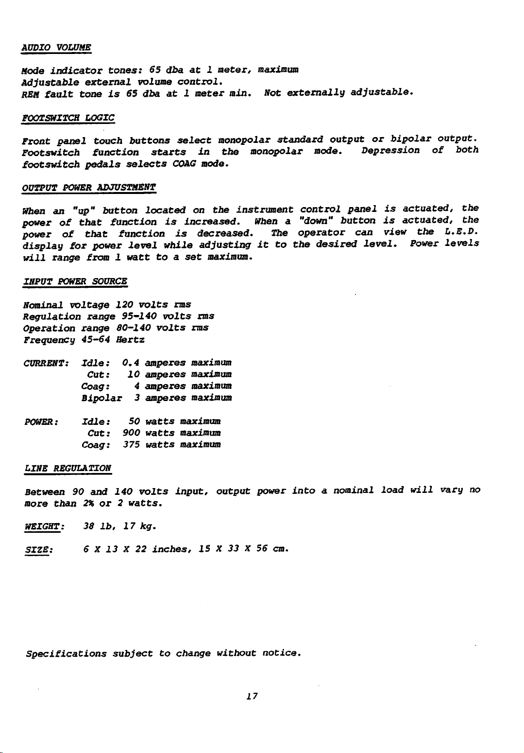
300
200
o
a.
100
100
200
500
1000
2000
RESISTANCE/OHMS
FIGURE
4
OUTPUT
POWER
VS
LOAD-MONOPOLAR
18
OUTPUT
Page 22

CO
1
C
UJ
$
O
Ql
70
56
42
28
a
•
*
PRECISE
MBP
STANDARD
MBP
14
10
20
OUTPUT
50
POWER
100
RESISTANCE/OHMS
FIGURE
VS
LOAD
5
-
BIPOLAR
19
I
150
200
OUTPUT
500
1000
Page 23

<
UJ
BIPOLAR
400
300
g
O
< .
200
100
0,000
8000
n
MONOPOLAR
10
20
30
CONTROL
40
SETTING
50
60
70
COAG
z°-
UJ
0.
o
6000
4000
2000
BLEND
3
CUT
0
MODE
MAXIMUM
OUTPUT
CONTROL
FIGURE
VOLTAGE
VS
20
SETTING
6
CONTROL
SETTING
Page 24
SECTION
6
CIRCUIT
POWER
The
DESCRIPTIONS
SUPPLY
FORCE4power
required
across
the
detector
voltage.
all
connected
voltage.
board
has
transistors
use
extreme
Supply
The
-5V
Tl,
and
regulated
+5V
Supply
MODULE
by
the
output
capacitors.
There
The
the
mounted on
caution
supply
rectified
by
Ul.
supply
generator
transformer
are
four
together
large
high
voltage
when
originates
by
module
circuitry.
There
returns:
at
circuit
the
probing
on
CR2. The
primary
are
pins
board
output
large
the
generates
It
and
four
analog,
1-4
of
is
components.
heat
sink
the
board.
Supply
rectified
the
also
R3
supplies:
digital,
the
and
transformer
the
controller
are
Module.
regulated
contains
which
discharges
+5V,
Controller
The
connected
Input
AC
is
two
high
and
output
power
filtered
and
isolated
load
-5V,
voltage
PCB.
T2
directly
resistors;
the
output
+15V
Transformer
and
and
supplies the high
the
small
board
is
and
passed
by
to
the
C2,
DC
power
peak
high
chassis;
circuit
its
four
line;
through
C3
R2,
Tl
and
is
which
L07
constant
current
inductor
kHz.
reference
shuts
oscillator
+15V
This
CR01. The
a
the
pass
output
the
trigger
ripple,
provides
is
controlled
The
down
output
Supply
regulator
zener
reference,
device
exceeds
inductor
and
a switching supply with
the
60
current
increases
at
-0.
5v
of
1.25V
the
to
output
diode
on,
current
with
runs
overvoltage
microhenry
equal
and
7v
and
by
U01
output
to
oscillator
duty
lower
duty
uses
voltage
CR02
voltage
comparator
current
the
reference.
hysteresis.
at
varying
the
which
is
enable
cycle
a
passes
protection
switching
to
the
when Q04
inductor
has
divided
when
is
cycles.
buck
is
divided
inductor
divided
U05
increases
through
This
frequency
15V
load
down
the
pin
50%
turns
At this
regulator
input and
current.
is
off
current
an
internal
by
output
14
and
regulation
down
by
on
in
CR01.
and
by
firing
buck
inductor,
CR03
decreases.
R13,
and
turn
drops
with
R27, R38.
the
by
LI,
time,
pass
R34,
pass
the
Note
controls
duty
5V
output.
SCR01
When
holds
oscillator
R14
and
on
0.33
is
device
R35,
When
device
0.75
the
pass
that
cycles
U2
to
clamp
operating
Q04
is
the
input
The
duty
running
compared
Q04.
volts
accomplished
U05
the
as
and
the
via
mH
device
is
the
A
below
Q01
R37
output
Q02,
inductor,
wired
output
load
is
a comparator
the
at
on,
the
side
cycle
at
to
second
pin
by
and
catch
and
is
Q03.
is
shut
as
voltage
is
output.
a
nearly
inductor
of
of
about
an
internal
comparator
13.
gating
diode
compared
less
With
until
off
a
schmidt
varied.
the
Q04
25
The
the
to
than
the
the
and
and
21
Page 25
Ancillary
detection
is
the
current
R33.
volts.
output
through
CR05
circuits
of
loss
and
of
crowbar.
the
Q07
shut
provide
the
U06
sense
-5V
off
over
supply.
is
the
resistors
the
voltage
comparator
+15V
CR06
R05,
supply
protection,
is
the
which
R06
exceeds
when
over
the
voltage
shuts
-5V
current
off
the
supply
limit
limiting
sensor
the
goes
and
supply
adjusted
below
and
SCR2
when
by
-3
High
This
input
tap
Voltage
supply
is
of
produce
bridge
which
has
a
catch
from
CR1901,
Drive
equal
with
are
its
current
diode
transformer
pulses
pulse
the
U08/1,
Q05,
C25,
a
voltage
The
set
Q06
the
slowly
error
point
voltage
and
actual
millisecond
provided
T2.
variable
CR4
located
own
source
CR1902
U09
the
to
astable
varying
is
less
voltage
output
Supply
is
an
Transistors
and
smoothed
return
function.
prevent
are
widths
output,
pulse
drive
than
voltage
taken
voltages
time
off-line
by
CR5
width
on
the
wire,
under
T1901
generated
in
width
the
capacitor,
error
the
is
the
generated
from
and
constant
pulse
and
CR3
Q1901, Q1902,
AC
pulses
by
inductor
St
rip
line
labeled
low
duty
Drive
on
saturation
for
the
by
a 2
phase
to
eliminate
controller.
primary
and
voltage
error
voltage.
amplified
in
the
high
its
binary
due
to
width
at
the
cycle
output
of
an
drive.
of
its
and
the
R41,
modulated
in
the
Q1903
the
L2
PCB.
high
conditions
Q1901,
the
astable
overlap
The
T1901.
ramp
the
and
Clock/Control
voltage
output
C22.
module
and
secondary.
and
capacitors
The
negative
voltage
Q1902,
PC
A.
transistors.
U09
The
in
variable
Pulse
waveform.
output
(See
page
integrated
bus.
is
R61
push-pull
and
Q1904
return.
and
Q1903
The
divided
U04
outputs
time
width
width
drive
41.)
U07/1
integrated
is
the
fed
to
conduct
The
output
C1103,
side
a
bridge
and
tapped
by
and
pulses
control
The
ramp
is
enabled
difference
PCB,
and
compares
comparison
switching
the
is
C1104
of
these
Inductor
CR4
Q1904
winding
2
in
are
logically
with
are
is
between
the
by
U07/2
type.
primary
alternately
rectified
and
capacitors
L2
performs
is
supplied
and
U04
to
the
output
amplified
by
U08/1
compared
when
the
actual
the
set
with
calibration.
center
C1105
acts
diodes
ensure
ANDed
Vs,
point
the
uses
with
ramp
the
high
a
DC
to
by
as
of
by
15
Several
set
ready
U08/2
is
the
when
output
below
signal
disables
U08/11
AND
protection
zero,
from
current
is
gates.
disabling
the
the
limit
pulled
circuits
CPU PCB
output
below
R62
are
the
is
AND
comparator.
U08/10
is
the
current
provided
ramp
high,
gates
for
comparator,
indicating
when
The
output
the
comparator
limit
22
the
the
+5
current
calibration.
supply.
by
a
volt
latches
U07/13
standby
supply
The
is
error
and
U07/14
condition.
is
sampled
low
and
voltage
lost.
by
disables
when
U08/13
R07
is
the
and
the
Page 26
INTERFACE
The
function
measurement
the
FORCEAElectrosurgical
of
circuitry
return
return
This
of
the
ground
measurements
The
purpose
located
panel.
monopolar
for
other
are
provided
important
the
FORCE 4
PRINTED
fault
electrode
assembly
electrosurgical
during
on
the
These
outputs
assembly
that
and
which
monitor,
on
of
generator.
CIRCUIT
of
the
control
monitor
contains
operation
or
handling
the
stripline
networks
(for
between
these
interface
functions
are
contained
lamp
(REM).
components
unit
output
example
modules.
components
spacings
ASSEMBLY
unit
enable
and
of
the
this
networks
assembly
provide
Physical
be
printed
which
with
in
circuit,
which
they
FORCE
assembly
with
the
C102),
of
maintained
circuit
link
the
microcomputer
this
are
are
4.
during
are
to
the
necessary
and
spacings
this
module
the
monopolar
assembly
keying
connected
at
high
Use
operation.
connect
output
provide
of
for
assembly
control.
are
isolating
to
voltage
extreme
the
jacks
series
the
approximately
and
other
continued
is
to
perform
output
circuitry
The
the
output
circuit,
the
output
with
caution
output
located
when
transformers
on
capacitors
interconnection
1
modules.
safe
operation
sections
networks,
and
terminals
respect
making
the
front
for
modes
centimeter
It
the
of
the
to
the
is
of
Components
electrode.
however,
patient
amount
typical
Transformers
networks
present
in
this
to
T103
The
return
active
corresponding
dependent
circuit.
further
harmful
C110
These
they
have
to
ground
of
radio
currents
T101,
and
the
on
the
transformer
for
proper
fault
and
return
with
upon
If
electrosurgical
alternate
the
the
FORCE
FORCE4generator.
the
CR106
Further,
output
causes
causes
between
active
network.
C117, C118, and C140
voltage
a
bias
tripping
the
and
dependent
opposite
active
return.
and
R112
components
low
voltages
frequency
in
that
T103,
return
4
be
return
monitor
currents
this
radio
sum
exceeds
return
Active
Higher
from
to
be
electrode
serve
have
impedance
are
current
mode
fault
monopolar
maintained.
current
operation
so
and
T104
fault
provides
flowing
frequency
a
current
and
active
operating
reference
the
approximately
and
to
provide
high
to
under
that
monitor.
actives
operation.
sum
pre-determined
is
will
return
radio
at
the
patient
provide
T101
a
in
is
voltage
inhibitied.
currents
current
impedance
30
current
not
which
direction
related
ground
for
a
grounding
to
frequency
volts
output
T101
and
is
the
compared
in
be
to
the
interface
isolates
it
balanced
summing
monopolar
the
level
present
rms.
mode
ground
is
are
than
through
when summed
of
a
trip.
to
specified
the
a
line
current
C116
and
important
in
with
activated
an
This
during
summed
return
CR106
with
The
given
link
frequency
out
voltage
between
against
response
function
output.
a
reference
alert
function
in
network
the
above
level
load
to
so
that
provides
of
is
high
that
monopolar
is
the
opposite
causes
other
circuit
condition
the
voltages,
typically
phase
minimized.
the
insulation
with
between
A
which
asserted
assures
use
disabling.
provide
of
impedance
return
a
small
with
output
voltages
respect
voltage
output
that
of
sign
currents
function
between
the
is
and
the
in
an
23
Page 27
Adjustment
of
through C140.
as
it
appears
fixed
output
The
either
reference
at
indicator
the
J101-19.
cutting
radio frequency
this on
output
filtered
power
the
amplifier
by
is
coupled
CI25
this
The
net
across
dependant
lamps
power
interface
via
and
to
level
of
voltage
R125
on
or
by
upon
the
the
coagulation
available
board
C124
to
detected in
the
controller
impedance
between
developed within the
comparator
the
FORCE4front
from
are
as
CR105
U109.
through
U110.
five
volt
panel
modes
the output amplifier.
follows:
and
CR104,
A signal indicating the presence
J101-16.
active
Whenever
supply
which
are
enabled
current
rectified,
and
CR106
the
indicate
ground
network
the
voltage
comparator
by
the
The
is
coupled
limited
is
provided
is
measured 1
exceeds
places
activation
presence
a -
an
in
of
provisions for 1
from
by
the
CR108,
of
RF
Activation
capacitively
excessive
allowed
provide
input
keying
optoisolators
The
Interface
function
a matched
square
symmetrically
and
C114.
using the outputs
dependent
radio
to
isolated
voltages
switch
of
capacitor
waves
Voltages
upon
switching
coupled
frequency
float
6
to
states.
to
output
PCB
verifying
at
the
injected
the
independent
comparators
contains
from
resistive
- 3 and J105 - 4.
have
and
fast
matched
capacitor
edges
temperature
temperature
and
are
that the monitoring
electrode
coupled
differential
analog
present
resistance
electrosurgical
amplifier
signal
on
representing
J101
pin
components
to
volt
supplies.
from
acceptable
and
U103
output
currents
present
U105.
The
components
exactly
circuitry
and
also
currents.
U108
19,
calibrated
the
leakage
of
located
elect
currents
grounded
on
the
rosurgical
these
circuitry.
R143-147 and R149-152
in
U101
The
output
the
Interface
the
circuitry
return
form
pins
across
6
into
The
loading
drift
characteristics
coefficients.
opposing
will
and
102
of
the
PCB. ^
necessary
electrode
an
oscillator
and
8
of
the
tuned
the
tuned
network
voltages present across
across
in
the
in
the
oscillator
The
outputs
phase.
have
that the detected outputs
The
detected
and a range adjustment
the
measured
to5volts
value
active
active
switching
which
comparators
impedance
which produces 140
U105.
network
return
by
virtue
These
accessory
output.
Q103-106
are
to
support
These
comprised
are
detected
electrode
and
of
U105
two
components
provide
dependent
is
conditions.
signals
Clll
load
of
similar
pins
conditions
handles
To
driving
are
prevent
must
be
T102
well-defined
the
upon
fed
FORCE
the
through
4's
L101,
kilohertz
by
T105,
by
and
outputs
appear
U107
C112
as
C113
also
are \
J105
tuned networks ^
inductor
6 and 8 have J
assure
repeatable response to return ^
at
of
return
150
outputs
is
provided
ohms.
will
electrode
be independent
are
amplified
by R118.
impedance
of
by
The
is
The
following
FORCE
component
characteristics
4: 1)
types;
characteristics
characteristics
insulation;
5)
component
should
are
be
altered.
performed
of
the Interface
2) creepage
location.
with
24
PCB
distances;
Any
service
care
so
affect
the
safety
of
the T
3) component values; 4) J
operation
that
none
affecting
of
the
these
critical
Page 28
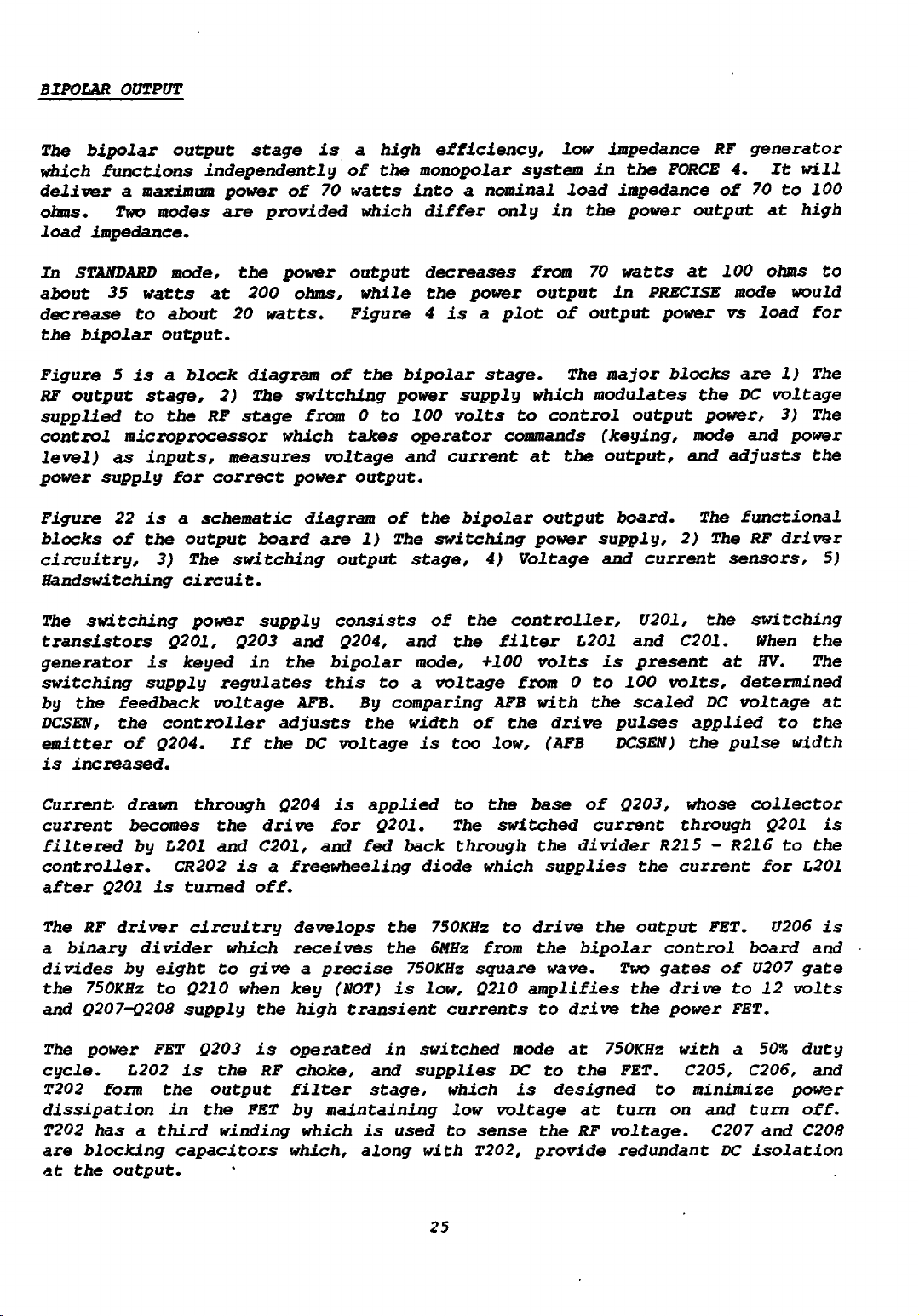
BIPOLAR
OUTPUT
bipolar
which
deliver
load
In
ahout
the
RF
supplied
control
level)
power
Figure
blocks
circuitry,
Handswitching
The
transistors
generator
switching
by
DCSEN,
emitter
is
functions
a
maximum
Two
modes
impedance.
STANDARD
35
watts
bipolar
output stage, 2)
to
microprocessor
as
inputs,
supply
22
is
of
the
3) The
switching
is
supply
the
feedback
the
of
Q204.
increased.
output
independently
mode,
at
output.
block
the
RF
for
correct
a
schematic
output
circuit.
power
Q201,
keyed
regulates
voltage
controller
stage
power
are
provided
the
200 ohms,
diagram
The
stage
measures
board
switching
supply
Q203
in
If
the
is
of
70
power
of
switching
from 0
which
voltage
power
diagram
are
output
consists
and
Q204,
the
bipolar
this
AFB.
adjusts
DC
voltage
a
high
of
the
watts
which
output
while
the
to
takes
output.
1)
to
By
the
efficiency,
monopolar
into
differ
decreases
the
is
bipolar
power
100
operator
and
current
of
the
The
switching
stage,
of
and
mode,
a
voltage
comparing
width
is
a
nominal
power
a
stage.
supply
volts
bipolar
4)
the
the
+100
of
too
system
only
from
output
plot
which
to
commands
at
output
power
Voltage
controller,
filter
volts
from
AFB
with
the
low,
(AFB DCSEN)
low
impedance
in
the
FORCE
load
in
of
The
impedance
the
70
power
watts
in
output
at
PRECISE
output power vs load
major
blocks
modulates the
control
the
L201
0
drive
(keying,
output,
board.
supply,
and
is
to
100
the
pulses
output
current
U201,
and
present
volts,
scaled
mode
and
The
2)
C201.
applied
the
RF
4.
of
100
mode
are
DC
power,
and
adjusts
functional
The RF
sensors,
the
at
determined
DC
voltage
pulse
generator
It
will
70
to
100
at
high
ohms
would
for
1)
The
voltage
3) The
power
the
driver
switching
When
HV. The
to
width
the
the
to
5)
at
Current
current
filtered
controller.
after
The
divides
the
and
The
cycle.
T202
dissipation
T202
are
at
Q201
RF
driver
binary
750KHz
Q207-Q208
power
form
has
blocking
the
output.
drawn
becomes
through
the
Q204
drive
by L201 and C201, and
divider
by
CR202
is
eight
to
turned
is
off.
circuitry
which
to
give
Q210 when
a
freewheeling
develops
receives
a
key
supply the high transient currents to drive the
FET
L202
a
Q203
is
the
in
third
capacitors
the
the
output
winding
is
RF
FET
operated
choke,
filter
by
which
which,
is
applied
for
Q201.
fed
the
the
precise
(NOT)
in
and
stage,
maintaining
is
along
to
the
The
back through
diode
which
750KHz
750KHz
is
low,
switched
supplies
used
with
6MHz
25
square
which
low
to
T202,
from
Q210
sense
base
switched
the
to
drive
the
amplifies
mode
DC
to
is
voltage
the
provide
of
current
divider
supplies
the output
bipolar
wave.
at
the
designed
at
RF
Q203,
the
Two
the
750KHz
FET.
turn
voltage.
redundant
whose
through
R215 - R216
current
FET.
control
gates
drive
power
with
C205,
to
on
minimize
board
of
to
FET.
a
C206,
and
C207
DC
collector
Q201
to
for
U206
U207
gate
12
volts
50%
duty
power
turn
and
isolation
is
the
L201
is
and
and
off.
C208
Page 29
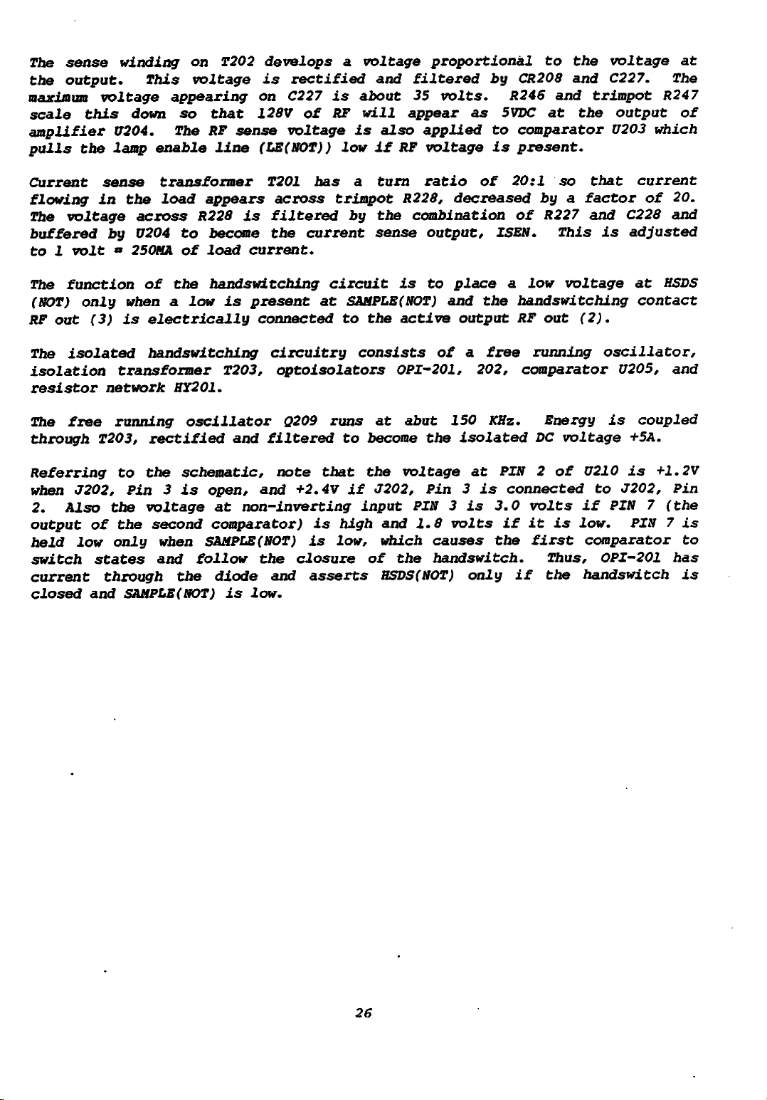
The
sense
the
output.
maximum
scale
this
amplifier
pulls
the
winding
voltage
down
U204.
lamp
This
appearing
The
enable
on
voltage
so
RF
T202
that
line
develops
is
on
128V
sense
(LE(NOT))
rectified
C227
of
is
RF
voltage
a
voltage
and
filtered
about
will
is
low
35
appear
also applied to
if
RF
proportional
volts.
as
voltage
by
CR208
R246
5VDC
comparator
is
present.
to
the
voltage
at
and C227. The j
and
at
trimpot
the
output
U203
R247
of
which
Current
flowing
The
voltage
buffered
to
1
volt
The
function
(NOT)
RF
out
The
isolated
isolation
resistor
The
free
through
Referring
when
2.
J202,
Also
output
held
switch
low
current
closed
sense
in
by
»
only
(3)
network
running
T203,
the
of
only
states
through
and
transformer
to
the
transformer
the
load
across
U204
250MA
when a
is
to
of
of
the
low
electrically
handswitching
HY201.
oscillator
rectified
the
schematic,
Pin
3
is
voltage
second
when
and
follow
the
SAMPLE(NOT)
appears
R228
is
become
load
current.
handswitching
is
present
connected
T203,
and
open,
at
and
non-inverting
comparator)
SAMPLE
(NOT)
the
diode
is
low.
T201
has
across
filtered
the
current
circuit
at
circuitry
optoisolators
Q209
runs
filtered
note
that
+2.4V
is
is
closure
and
asserts
a
trimpot
by
sense
SAMPLE
to
the
consists
at
to
become
the
if
J202,
input
high
low,
of
turn
R228,
the
combination
is
(NOT)
active
OPI-201,
abut
voltage
PIN 3
and
which
the
HSDS
ratio
decreased
output,
to
place
and
of
150
the
Pin3is
1.8
volts
causes
handswitch.
(NOT)
of
ISEN.
the
output
a
free
202,
KHz.
isolated
at
is
3.0
the
only
20:1
of
so
by
R227
a
This
a
low
voltage
handswitching
RF
out
running
comparator
Energy
DC
voltage
PIN 2
of
connected
volts
if
it
is
first
Thus,
if
the
that
current
factor
and
C228
is
adjusted
at
contact
(2).
oscillator,
U205,
is
coupled
+5A.
U210
if
low.
comparator
to
J202,
PIN 7
OPI-201
is
PIN 7
handswitch
of
+1.2V
20.
and
HSDS
and
Pin
(the
is
to
has
is
26
Page 30
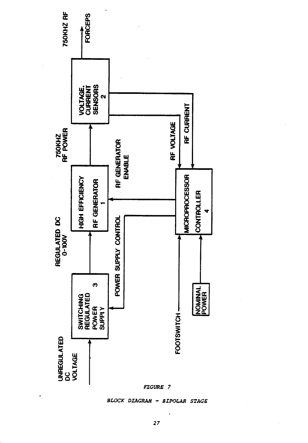
RF
750KHZ
POWER
750KHZ
RF
DC
FORCEPS
2
SENSORS
CURRENT
VOLTAGE.
1
EFFICIENCY
GENERATOR
RF
HIGH
GENERATOR
ENABLE
RF
i i
CURRENT
RF
VOLTAGE
RF
MICROPROCESSOR
CONTROLLER
4
0-100V
REGULATED
REGULATED
SWITCHING
VOLTAGE
DC
UNREGULATED
3
POWER
SUPPIY
to
CONTROL
SUPPLY
POWER
a
a
-
POWER
NOMINAL
FOOTSWITCH
NJ
hi
1
s
p
Co
CO
g
Page 31

BIPOLAR
The
and
bipolar output
The
CONTROL
BOARD
Bipolar Control Board
ECON)
and
sends appropriate signals
board.
Control
Board
analog-todigital
U301
and
miscellaneous
The
Control Board performs
received
(DSIE
or
receives
contains
conversion
logic.
DS2E):
the
(ADC)
the
signals
(KEY(NOT),
microprocessor
U313,
following
from
the
digital
functions
CPU
Board
reset
U307, program memory U302, «
to
(NOT)
analog
when
(DSE,
and
conversion
a
keying
DSIE,
AFB)
to the T
command
DS2E
(DAC)
is
1) Analog
power
70
The
and
2)
output
3)
ADC
4)
level
watts.
digital
the
The
After
reads
From
delivered
or
down
Figure 4 shows
PRECISE. The
100
ohms,
PRECISE
to
(0 to
reset
KEY(NOT)
output
board
a
will
delay
the
the
power
to
achieve
the
mode
digital
line
line
voltage
be
RF
output
voltage
and
the
two
STANDARD
reduces
conversion
70
watts).
is
10
of
which
enabled.
AFB
volts.
about
ECONisset
holds
is
20
mS
voltage
and
current
the load
the
required
required power vs impedance
modes
the
impedance
are
mode
output
identical
dropoff proportional to the square
5)
The
it
line
then
is
processor
goes
unasserted.
back
checks
to
step
for
DSIE
3. Otherwise,
of
the
the
power supply
initially
for
the
(VSEN)
and
measurements
and
power.
at
holds
voltage
of
or
the
the
DS2E.
control
voltage
ECON
sets
at 16.4 watts/volt or 4.25
controller
set
so
circuit
current
the
adjusts the
impedances
output
as
the
impedance
resistance.
If
AFB
is
that
conditions
(ISEN)
for
voltage
the
set
the
DC
to
microprocessor
feedback
the two modes
below
generator
to
constant
rises,
zero
100
and
the
off
is
voltage
stabilize
computes
voltage
STANDARD
ohms.
while
giving
is
still
the
nominal m
volts
for j
disabled
on the ^
the
the
AFB
up
and ^
Above
the
a
power
keyed,
KEY(NOT)
U305 and
periodically
transistor
the
processor
out
within
and
off
used
the
reset
5
(NOT)
and C307
as
the
volt
the
reset
Q301
fails,
1
second.
low.
discharges.
reference
reference
associated
by the
at
20
MSEC
it
The 555
The
for
intervals,
will
timer
CR301
voltage
the
gates
form a
processor.
stop
ADC.
output
will
is
for
issuing
the
'watchdog'
The
keeping
these
is
pulled
reinitialize
a
precision
DAC
and
28
processor
the
voltage
pulses
low,
when
2.5
is
amplified
which
timer
the
volt
pulses
across
and
forces
generator
reference
which
the
by
the base
C309
555
will
key
(NOT)
is
U312
to
must be
of
low.
time
high
turned
which
become
If
is
Page 32

TABLE 1 INPUT & OUTPUT
ANALOG/
NAME
DIGITAL
LINES
VOLTS
- BIPOLAR
DESCRIPTION
CONTROL
DSE
DSIE
DS2E
ECON
DCSEN
ISEN
VSEN
AFB
KEY
D
D
D
A
A
+12
+12
+12
+5
+5
+5
+5
+5
+5
Master
Desiccate
Desiccate
Note:
Test
Analog Power
Watts
Scaled
Scaled
RMS
Scaled
Volts
Analog
20
Low on
Stage
Desiccate
Mode
Mode
DSE
Routine
DC
Supply
RF
RF Load
RMS VSEN =
Drive
Volts
key
DSIE
Set
Load
to
enables
Enable
1
Enable
2
Enable
Voltage:
Voltage:
Current:
Voltage:
ISEN@100
Switching
RF
-
DS2E
drive
From
Causes
1
1
Volt:
1
Volt
1
ohm
Supply:
to
CPU
Volt
Volt
Board
entry
20
=
Load
the
=
Volts
2.56
=
1
Volt
Output
to
16.4
ma
25.6
=
RESET
FSDS
HSDS
+5
Low
on
Footswitch
Handswitch
29
RESET
holds
Desiccate
Desiccate
the
Power
Enable
Enable
Supply
off.
Page 33

CENTRAL
The
functions
provide
which
the
purposes
be
treated
The
second
of
the
conditions.
interpreting
analog
when
control
keyed
voltage
audio
tones
produced.
assurance
PROCESSOR
of
the
interface
status
of
discussion,
as
an
function
generator
In
key
and
EREM
(REM
associated
A
"watchdog"
of
proper
UNIT
the
of
extension
of
in
addition
closures,
voltage
generate
output)
program
(CPU)
CPU
through
various
the
the
response
ECON
the
with
BOARD
Board
systems
front
of
the
CPU
to
to
the
(energy
associated
must
keying
timer
operation.
fall
which
panel
CPU
Board
operator
interfacing
CPU
be
sensed
under
into
the
within
keyboard
Board.
is
to
Board
control)
logic
and
program
two
FORCE
the
provide
input
with
must
input
and
various
categories,
4
is
generator
and
control
as
well
displays
calculate
which
to
processed
alert
control
controlled
display
as
scales
other
on
provides
the
first
are
displayed.
assemblies
of
other
various
and
and
the
circuits.
the
conditions
being
and
subsystems
internal
sensing
generate
output
CPU
card
must
continuous
to
through
For
will
and
the
power
Analog
and
be
The
8039
CPU
address/data
bits
line
at
U403
status
K1102,
addressing
of
allowing
the
is
address
positive
a
bidirectional
of
11
strobes
and
asamultiplexed
Keyboard/display
segment
closure
interface
The
configured
every
displays
of
card.
display
as
10.3mS
accordingly.
which
accessing
Front
scan
8279
low,
Logic
lines
is
software
is
panel
lines
are
thus
input
allowing
stored
only
the
switches
are
internally
a
in
control.
addresses
bus
at
the
transition
front
the
data
4
interface
various
consists
an
while
This
updated
display.
common
key
is
read
the
a
and
the
the
instruction
panel
isobloc
transfer
bit
and
eight
switches
8
by
data
are
biased
closure
input
64
bit
4K
lower
negative
of
the
16
bit
lamps,
circuit
is
address/data
U410
status
of
eight
8
matrix.
the
corresponding
is
stored
as
needed,
arranged
to
the
high.
will
similarly,
to
be
sensor
bytes
four
transition
fetched
PSEN(NOT)
I/O
via
and
and
seven
LED
be
with
sensed.
RAM
of
bits
expander
enables
and
the
bus
3
to
LEDs
read
The
in
a
thus
as
elements
array.
The
sensed
which
program
of
from
steering
resets
lower
when
8
line
on
the
handswitch
segment
eight
segment
64
bit
freeing
Return
scan
as
tri-state
Input
port
of
U407
line.
through
4
this
front
displays
display
in
lines
a
logic
data
may
memory
2.
the
ALE
to
the
bits
device
decoder
displays
drive
the
an
lines
buffers
is
be
via
U406
(address
be
transferred
which
and
cut
"watchdog"
of
port
is
U402
panel
related
and
are
RAM
processor
8
by8matrix
RLO
are
sequentially
zero
updated
accessed
latches
the
relays
2
accessed.
drive
assembly,
eight
scanned
lines
internal
through
on
one
enabled
the
CPU
which
logic
from
every
as
latch
are
needed
multiplexed
the
lower
enable)
to
the
controls
K1101
timer.
functions
the
eight
sense
from
mode
sequentially
asserted
to
the
continually
in
which
RL7
of
asserted
return
by
the
10.3mS
8
bus
the
and
U403
7
the
the
lamps
8279
the
the
line.
scan
and
under
30
Page 34

ECONisproduced by
current
selecting
executingaMOVX
low
address
order
to
FB,
voltage
via
eight
which
address
instruction.
bits
selects
U416,
a
converter.
line
to
address
the
ten
bit
U416
A2 and
Data
is
FA,
BYTE2(N0T)
digital
is
addressed
strobing
transferred
then
writing
input
to
the
mode
analog
as
WR(NOT)
in
the
for
converter
external
two
bytes
high
U416.
memory by
(write)
by
order
and
U415,
line
writing
two
bits
a
chip
by
the
to
Keying
level
ECON
through
input
volts,
keying
U417
EREM
requires
will
executing
Sections
the
generator
for
the
mode
is
calculated
is
the
input
is
every
and
ports
released,
an
1 and 2
presence
and
eight-bit
20
WR(NOT)
640 microseconds.
be
interrupted
a
MOVX
1
and
providesasignal
U421
and
U428. The
multiplied
strobing
address
which
level
V0L1
drives
will
and
through
chime-like
U418 and
every
20
by
the
the
CS(NOT)
F7. U420
the
be
constant
V0L2
the
keyboard
tone
then
mS.
initiates
actuated
and
written
the
mode
of
produce
analog
mS.
2
read
of
to
The
are
via
instruction
U421
a
variable
audio
ratio
line
is
a medium
loudspeaker
when
volume
control
interface
will
diminishing
be
is
of
U414
and function
a
REM
an
alert
to
conversion
enabled
When
the
are
a
level
data
of
power
located
the
created
the
the
following
retrieved
to
U416. Mode
and
buffers
from
enables
fault
digital
INTR(NOT)
two
in
U418
switches
level
or
return
indication.
converter
is
initiated
by
a
MOVX
the
at
address
tone
gain audio
at
PIN 8
write
conversion
line
EF.
oscillator
amplifier
of
U421
(U418) / 255. The
by
executing
OP-AMPina
in
the
generator
U410.
by
first
to
is
in
When
zero
the
writing
program sequence. The power
RAM
and
the
and
U411
cease
fault
instruction
and
bridge
control
keyed,
control
an
alert
in
function
and
condition
which
when
is
conversion
which
comprised
is
the
a
MOVX
panel
and
the
55
successive
required
enables
U413.
and
ECONisset
processes
the
chip
at
complete,
runs
level
audio
write
amplifier
LS1701. The
will
beafunction
panel,
condition
maximum
When
will
continuously
of
at
level
which
audio
value
are
the keying
cancel
analog
select
address
the
processor
data
section
PIN 1
is
instruction
configuration
are
is
present,
steps
for
written
to
zero
the
input
line
EF
and
read
and
3
of
U421
set
audio
of
read
level
occuring
by
of
by
to
a
to
U404
event
or
less
enables.
U405
is
a "watchdog"
of
a CPU
by
the
The
during
the
failure.
CPU,
timer
"Power
timer
will
is
reset
On"
which
It
is
time
by
sequence.
a
out
defeats
oneshot
causing
the
master
all
mode and
timer
output
31
reset
which
PIN 3
generated
function
if
not
to
go
reset
low
by
enables
every
defeating
two
sections
in
500
the
mS
all
of
Page 35
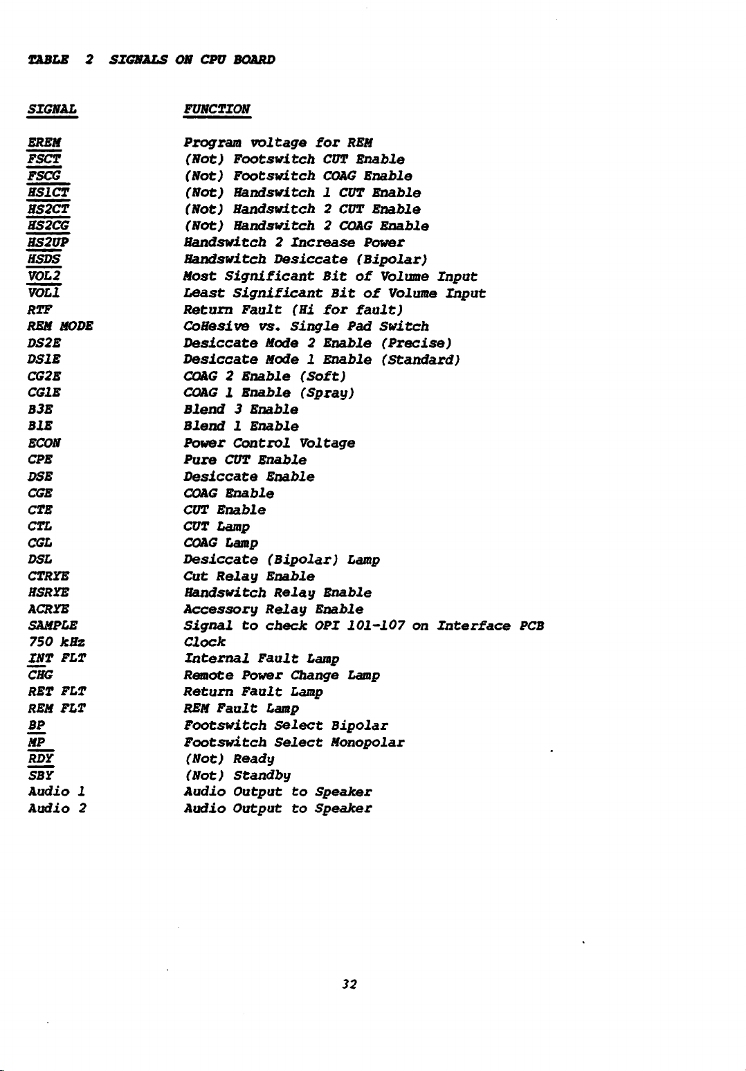
TABLE
2
SIGNALS
ON
CPU
BOARD
SIGNAL
HS1CT
HS2CT
HS2CG
HS2UP
HSDS
FUNCTION
Program
(Not)
(Not)
(Not)
(Not)
(Not)
Handswitch
voltage
Footswitch
Footswitch
Handswitch
Handswitch
Handswitch
Handswitch
Most
Significant
Least
Return
CoHesive
Desiccate
Desiccate
COAG2Enable
Significant
Fault
vs.
Mode2Enable
Mode1Enable
COAG1Enable
Blend
Blend
Power
Pure
Desiccate
COAG
CUT
3
1
Control
CUT
Enable
Enable
Enable
Enable
Enable
Enable
CUT Lamp
COAG
Desiccate
Cut
Lamp
Relay
(Bipolar)
Enable
Handswitch
Accessory
Signal
Clock
Internal
Remote
Return
REM
Fault
Relay
to
check
Fault
Power
Fault
Lamp
Footswitch
Footswitch
(Not)
(Not)
Audio
Audio
Ready
Standby
Output
Output
for
CUT
COAG
1 CUT
2
Increase
Desiccate
Bit
(Hi
for
Single
(Soft)
(Spray)
Voltage
Relay
Enable
Enable
OPI
Lamp
Change
Lamp
Select
Select
to
Speaker
to
Speaker
REM
Enable
Enable
Enable
2 CUT
2 COAG
Enable
Power
(Bipolar)
of
Bit
of
fault)
Pad
Lamp
101-107
Lamp
Bipolar
Monopolar
Enable
Volume
Volume
Switch
(Precise)
(Standard)
on
Input
Input
Interface
PCB
32
Page 36

CLOCK/CONTROL
The
Clock/Control
initiate
supply
to
the
signals
or
saturation
The
in
U615,
and
bursts
used
voltage
card
board
is
gated
for
in
and
from
generates
a
the
terminates
signals.
derived
with
and
is
HW
sets
reset,
flip-flop
To
discuss
The
coag
U607/6,
a
In
from
32
used
the
(VR).
reset
control
and
transistor
also
exceeds
At
the
terminates
U605
on
that
the
drive
transformer
pulse
pulse
output
terminated
the
instance,
below
high.
increases
HW
by
width
(CSCG). When
OND
voltage
the
clamp
If
well
going
the
high,
same
BOARD
terminate
are
the
of
dual
by
the
coag
the
the
the
kHz
as
maximum
It
the
by
Q602
on
three
primary.
possible)
via
by
HW
on
if
CSCG
CSCG
amount.
PCB
by
generating
a
750
sense
the
output
six
4
bit
the
cut
blend
modes.
on
drive
cut
hemostasis
repetition
a
flip-flop
occurs
in
circuitry
pulse
sequence
HW
which
and
allows
the
off
C601
inputs
signal
CSCG
U601.
via
U605/6.
C601
above
and
which
doesn't
voltage
occurs
U602's
generates
each
kHz
board;
clock
counter.
clock
outputs.
modes,
rate
on
time
at
width
goes
drive
the
high
HW,
OND
The
primary
or
until
occurs
For
on
soon
the
C602
CGVCM
the
RF
pulse.
Vs,
the
clock
and
CSCT,
transistors.
signals
The
enable
MC
The
gate
at
U601/2
G
is
window
(16
reset
in
the
a 4
kHz
controlling
control
is
initiated
high
current
by
speed
CGVCM,
goes
current
the
U619/4
a maximum
Pulse
is
the
occur
C602
and
after
clamp
signal
on
It
power
mode
CSCG,
by
master
(CCE)
is
not
clock,
independently
derived
(HW).
kHz
in
circuits
coag
and
circuitry,
at
the
source
forcing
comparator
and
high
sense
clears
pulse
width
average
then
the
HW
voltage
(OND)
also
and
controls
supply
enable
S, OS, which
dividing
clock
to
provide
gated
(G),
from
HW
and
in
coag
controlling
modes.
is
mode
the
power
we
by
CL
same
the
initiating
increases
PCB
regulation
C601's
coag
goes
going
Q601
G
width
value
and
time.
high.
flip-flop
generates
the
pulse
high
high,
off
(OFD)
programming
signals
down
signal
in
pure
controls
of
MC.
2).
independent.
In
the
CL
The
supply
will
which
sets
HW
to
charge
When
U602
output
changing
until
flip-flop
CSCG
of
voltage
there
never
is
the
starts
then
and
control
the
high
from
indicate
the
(MC)
25%
and
cut.
the
any
the
clock
is
not
output
last
set
examine
flip-flops
high
capacitor
the
Q
output
HW
the
COAG
and
done
flip-flop
decreases
as
the
will
be
the
OND
voltage
voltage.
the
current
750 kHz
occurs
50%
Neither
off
other
coag
(CL)
mode
clock
VR
point.
COAG
turns
voltage
(CGVCM)
of
goes
current
terminates
occurs
by
changing
soon
voltage
a
delay
will
signals
CPU
CPU
at
duty
drive
on
modes
are
dependent
pulse
is
is
used
in
off
goes
are
the
low
and
output.
until
as
be
power
Input
and
four
limits
clock
750
kHz
cycle
clock
and
drive
G
signals
width.
voltage
as
detail.
U601/4,
clamp
C606;
on
C606
high.
high
and
output
(maximum
sense
the
OND
For
it
HW
goes
on
C601
between
delayed
to
is
is
a
HW
is
is
Two
additional
step
microseconds
until
SS.
the
circuit
saturation
circuits
It
is
after
coag
is
a_
(S)
pulse
one
millisecond
or
oversaturation
are
generated
HW
goes
is
involved
when
low.
over
HW
Its
and
one-shot
(OS)
with
goes
function
prevent
which
pulses.
33
the
coag
high
false
is
pulse.
and
is
to
computations.
triggered
persists
stop
The
the
first
by
is
single
for
about
microprocessor
The
second
the
sense
5
PCB
Page 37

The
one-shot
also
shorter
The
width.
on
which
The
clock
The
CSCT
LED,
drives
CUT
C610
is
CUT
flip-flop
or
CR601,
Voltage
supply
The
test
U606/10,
the
flip-flop.
The
power
set
by
integrated
to
either
pulses
and
set
pulse
The
to
the
enabled
flip-flop
cleared
the
mode
point
for
U606/11
supply
the
by
4.0
output
the
coag and
and
width
MC
clock
rapid
by
output
saturation
indicates
operation
VMO/CMO
is
set
VR
clock
U621/14
or
2.4V
(M)
boosts
is
unclamps
ramp
the
is
by
the
passes
exceeds
set
point
to
by
asserts
cut
the
controlled
on
CCE
clock.
comprised
current
signal
current
(VMO)
8V
is'
also
and
controller
and
cleared
generate
the
R645,
pulse
power
C604
C604.
of
through
(S)
mode
with
and
done
forces
the
sense
as
the
Vs.
R646,
OFD
width
supply
in
and
C610
U610/4
a
the
operation
S
in
generator
at
VMO
by
and
control
set
a
U603
is
cut
gate
input
control
the
operation
uses
S
In
the
R647
terminates
point
manner
compares
driven
and
(CSCT)
array
VR
clock
flip-flop
or
OS.
dessicate
network.
circuits
voltage.
similar
by
U607/9.
pulse
U612
to
transmission
(CMO)
always
is
driving
until
The
any
output
in
to
a
slowly
transmission
It
is
from
which
with
rate
U606/4,
occurs
when
CSCT
flip-flop
or
COAG
CSCT
a
the
direction
the
varying
set
the
sense
selects
gate
in
when
high
the
occurs,
U605/10.
mode
pulses.
COAG
voltage
gate
by
U611/3
the
board.
either
U611.
control.
the
impedance.
flip-flop
clearing
It
output
Vs
is
M
of
pulse
CL
An
power
is
is
set
34
Page 38

750
KHz
JTJTJlJTJTnJTJTJ^^
LO
CONTROL
L0«
A Q3
I 1
CONTROL B Q1
LO-
1.33MSEC
i 1
•
J 1
CONTROL
LO-
CCE
LO-
CCE
HI'
CCE IF
HI-
MC
L0«
HW
LO-
cl;
LO
U602
B Q2
IF
CPE
IF
B1E
(B-iE'CPEI
IF IB2E > B3EI
vr=cl
PIN
U602
clk/cntrl
PIN
2
FREQ.
= 31.25
= IF IB2E* B3EI
5.33
J
bd
n
*i
u
3
ITYPI
670
KHz
MSEC-
q8oi
CNTRLB0603
7.80
SAME
PRR*7.81
V
PEAK
SCALE
-nJTJXTLTLT
KHz
AS
ABOVE
3.9
VDC
U602
L0«
MC
LO-
U603
U603
HI-
NOTE:
PIN
U603
PIN2ITYPI
PIN
PIN
Propagation
7
3
7
1.33/<SEC
discrepancies
TIMING
WAVEFORMS
not
shown.
FIGURE
-
CLOCK/CONTROL
8
BOARD
35
Page 39

VS
••
OFD
OND
LOGIC
OUTPUT
I
(S)
KEYING.
SUPPLY
CONTROL
VCM
COAG
COAG
CONTROL
VCM
CUT
CUT
CONTROL
M
ONE
SHOT
(OS)
SENSE
SENSE
CLOCK,
8
1
to
to
ti
8
Page 40

BOARD
The
Sense
regulation
sense
signals,
The
sources.
voltage
indicate
volts
go
U807)
saturation
FORCE 4
by
below
with
divider
The
current
two
comparators.
been.
processed
COAG
are
signals
reached/
as
operated
current
VR803. A
units
inputs
with
resistors
R844,
comparator.
867.
Board
of
one
To
supply
that
R803
about
and
by
well
to
source,
bias
differential
are
R829,
generates
output
of
for
CUT
output
insure
is
saturation
and
10
one
input
the
second
drawn
the
the
as
reducing
at
logic
Q801,
voltage
connected
844,
The
CSH, CSL
pulse
the
output
and
one
transistors
class
boosted
is
the
OS
signal
volts.
from
input
from
When
Clock/Control
the
CSCT
HV
levels.
the
the
and
the
level
with
is
inputs
to
857, 867.
voltage
logic
width
for
C
for
occurring.
Both
signals
and
transistors
COAG.
are
operation
high
is
signals
the
output
the
designed
load
fixed
fromareference
HV
supply
comparators
CSCG
Board
length
and
The
high
voltage
supplied
and
CSH, CSL
The
is
signals
and
of
optical
comparator
by
output
inputs
difference
used
high
and
under
resistances.
TheSsignal
and
are
collectors
sensed
trip,
are
terminate
the
next
couplers
power
compliance
Q802.
current
(current
are
must
on
the
voltage
two
are
to
operate
varying
occurs
generated
voltage.
by
the
indicating
generated.
the
output
supply
anda10V
The
amplifiers
sense
biased
exceed
Clock/Control
set.
point.
output
class
load
is
when
through
(U802,
comparators
conditions
The
calibrated
the
by
foil
the
present
pulse.
comprises
high
off
by
the
Two
as
current
C
S
and
at
output
comparators
a
23:1
resistor
current
These
804)
signals
output
The
translate
comparators
voltage
are
Q803,
and
low)
currents
bias
to
Board
signals
as
current
the
OS
signals
about
collectors
(U806,
resistive
board
limit
pulse
a
40
regulator
discrete
804.
through
through
trip
for
sense
high
30
and
has
are
in
the
mA
The
the
The
comparator
generated
the
sources
U805.
power
program)
voltage
The
gates
current
power
pots
adjusted
calibrations
calibrations
The
calibration.
CGPG
U808
setting
R805,
by
output
Q809,
U805
which
to
current
voltage
and
limit
at
the
806
high
for
off
805
pots.
in
and
for
CPU
power
with
op
are
converter.
is
Blend
R804
are
power
cut
coag
bias
amp
and
Board.
setting.
high
offset
The
calibrated
generated
The
3
depends
controls
the
power
power.
voltage
input
gates
pure
levels.
current
This
is
by
voltage
The
adjusted
to
by
R806,
the
are used to
on
the
cut
and
Thus
output,
limit
is
bias
compliance.
U805
ECON
the
coag
37
and
currents
by
is
805.
voltage
cut
pulse
coag
R802,
R801,
is
controlled
proportional
R801,
CTPG,
U805,
alter
power
current
power
R806
by the
to
the
are
generated
The
current
802
and
CGPG
Q805,
passing
is
this
(cut
Q809
through
CGPGinBlend 3.
setting
calibration
are
R805
level
are
rather
the
in
offset
the
ECON
controlled
provides
program,
constitute
square
by
voltage
current
transmission
The
than
the
Blend
pots
corresponding
3.
and
and
root
a
coag
coag
coag
gain
by
low
a
The
are
Page 41
Regulators
circuits.
807
are
level
Q808,
is
not
VR801
R821
used
and
and
shifters
at
VR802
L801
on
present.
provide
isolate
the
the
optical
clean
HV
comparator
coupler
+12V
and
power.
outputs.
-2.5V
The
power
Q810,
display
to
811
the
board
and
Q806,
blanking,
DRIVER
The
driver
1)
2)
3)
The
HVCL
nominal
reference
turns
high
cascades
The
Q1006.
voltage
output
generated
by
the
on
the
shouldn't
BOARD
board
Drive
and
Sense
peak
module.
the
put
the
detector
the
Amplify
and
T/OFF.
(high
on
4.75V
is
Q1001
reference
exceeded,
to
return
drive
of
three
CR1001
by
and
Q1008,
R1022, R1019
falling
exceed
in
the
output
cut
high
the
OND
voltage
connect
on
signals
transistors.
CR1002
edge
0.1
FORCE 4
relays
inductor
voltage
capacitors
and
clamp)
level
a
pins
T/ON
around
Q1003
and
divider.
of
T/ON
microsecond.
has
to
in
clamp
through
OFD
turn
level
(adjust
20
microsecond
the
load
3, C. The
and
The
Q1007
Q1002.
The
because
three
select
the
level
on and
resistor
T/OFF
on
off
Q1002
functions:
the
output
and
R3
turn
is
divided
with
one-shot
reference
are
generated
drive
eliminate
The on
drive
is
is
handswitch
collector
discharge
(750
(R3
ohms)
off
by
R1001)
in
is
regulated
signals
100
(U1002)
the
from
is
amplified
saturation.
drive
to
is
-5V.
used to shut
or
circuit.
the
in
and
by
power
OND
by
about
There
footswitch
output
the
power
to
generate
compared
U1001.
is
triggered
supply)
by
CR1003.
and
Q1001,
The
+10V,
is
some
off
Q1006
collector
When
OFD
Q1007
off
drive
controlled
output
supply
T/ON
to
the
and
to
the
by
two
and
overlap
but
a
is
it
VR1001
provides
regulated
+12V
power
to
the
board
33
circuitry.
Page 42

STRIPLINE
The
Stripline
current
three
relay
the
cut
in
COAG
BOARD
sensing
relays.
K1102,
inductor
modes.
Board
resistor,
One
selects
in
contains
relay,
the
the
the
high
K1101,
handswitch
cut
mode
driver
and
transistors
voltage
selects
output.
selects
power
the
The
a
for
supply
accessory
third
tap
on
the
filter
the
output
output.
relay
output
modules,
capacitors
The
K1103
connects
transformer
a
and
second
There
are
followers
current
as
emitter
bases
The
low
current
J1102.
(current
are
input
power
setting
The HV
This
supply
high
The
handswitch
drives
the
to
E4,
winding
frequency
output
cut
alter
5,
voltage
primary
henries.
three
to
sharing.
followers
when
The
load
sense
to
supply
module
jack
the
footswitch
inductor
the
6,
and
supply.
inductance
turn-on
the
both
sensor
current
high
a
comparator.
on
the
is
is
full
and
noise
load
and
output
the
The
T/ON
Three
T/ON
is
a
20
C1103,
is
and
current
is
signal.
turn-off
to
and
a
and
control
kHz
wave
above
either
connects
jack
CHOI,
tuning.
output
2.5
transistors,
the
T/OFF
T/OFF
low
inductance
is
sensed
low)
signals
The
panel.
switcher
rectified
1104,
the
switching
Tl,
and
connects
1102
All
sense
transformers
and
12
1.5
transistors
signal.
are
to
comparator
whose
1105
to
at
the
El;
are
three
resistor,
microhenries.
Q1104
ohm
not
control
are
and
the
frequency.
upper
or
to
placed
output
1105,
emitter
Q1101,
R1105
present.
0.05
sent
threshold
output
then
stripline.
T2,
E2.
across
which
have
1106,
resistors
1102, 1103,
holds
ohm
foil
the
output
to
the
is
a
filtered
transformer,
the
middle
In
addition,
the
coils
a
in
turn
3:7:32
The
have
cut
connected
ensure
the
resistor
power.
sense
changes
transformer
by
R1101
which
transformer,
transformer
one
connects
turns
inductor
output
board
with
L2
and
in
the
end
ratio
as
equal
are
connected
transistor
mounted
The
CSH, CSL,
where
the
secondary.
in
the
C1116
drives
cut
primaries
connected
to
the
and
is
2
emitter
load
at
they
output
power
reduce
the
which
modes,
to
high
their
micro
The
FORCE 4
performed
and
the output
is
the
from
transformer
inductance
transistors
the
generator
versus
load
load
is
at
a
resistance
front
losses.
is
are
output
impedance
a
controlled
300
power
panel
charged
on
resistance
ohm
and
current
load.
is
roughly proportional to R X [300/(R+300)]^
and
The
300
jacks.
In
the
to
a
this
stored
when
curve
is
flatter
machine.
generator
ohms
Most
coag
calibrated
the
is
the
of
modes,
energy
transistors
in
coag
39
In
acts
generator
this
the
current
is
than
the
cut
as
a
output
output
output
level
discharged
go
in
cut.
modes,
constant
resistance
transformer
into
off.
resistance
when
The
calibration
current
is
the
the
load
output
source
where
viewed
due
primary
output
and
power
is
R
to
Page 43

OUTPUT
The
modules
equal
wire
variation
The
inductance.
the
load
absorbs
the
turn
output
as
transistor
MODULES
FORCE4Output
are
currents.
loop
output
transistor
to
any
turn
off
transistor's
peak
connected
is
provided
due
to
load
This
prevent
transmitted
off
times
transistors
detector
is
mounted
The
V&g
is
reverse
Modules
in
are
parallel
identical
and
most important parameter
for
differences.
is
inductive
load
switched
of
Q1101,
base
for
the
onaheat
current
will
off.
bias
energy
the
drive
output
tend
five
1102,
sensing.
and C4
to
Diode
damage.
through
CR3
1103
when
transistor
sink.
reverse
diodes.
saturation
matching
is
CR3
disconnects
CR3
CR3.
on
They
are
to
those
ensures
is
A
0.1
used
bias
cannot
Capacitor
Diode
the
stripline
occurs.
collector
to he
used
the
ohm
to
the
turn
CR1
replaced
in
that
transistor
emitter
tune
the
collector
the
transistor
off
C3
is
is
board
Diode
voltage.
the
SSE3B.
all
of
fall
resistor
2.5
junction
instantly
used
used
to
and
CR2
as
matched
them
carry
time.
reduces
microhenry
from
and
to
equalize
drive
remove
and CI
Each
output
sets.
Five
A
when
the
CR4
the
the
act
Page 44

(A)
(B)
(C)
U2008.
U2008,
U2008,
U2009.
PIN
6-OSCILLATING
PIN
7-D.C.
PIN 1
PIN
3
^r
(D)
(E)
(F)
U2003,
U2003,
E=B«C«D
U2003.
E=B'C-D
PIN 11
PIN 9
PIN
10
OUTPUT
POWER
FIGURE
SUPPLY
41
10
TIMING
DIAGRAM
Page 45

+
HV
110
VAC
FOOTSWITCH
FRONT
PANEL
DISPLAY
AND
KEYBOARD
POWER
SUPPLY
1
s>
A—*s
^—/
i15
_+5
- 5
CLOCK/
CONTROL
CPU
+
HV
U/vvv
DRIVER
•
KEYING
STRIPLINE
OUTPUT
}£
AND
MODULES
r
ISOBLOC
ACTIVE
OUTPUT
TRANSFORMER
RETURN
Ml—1—!
/YYY^
I-
COAG
CUT
ii
REM
BIPOLAR
HV
BIPOLAR
CONTROL
+
HV
BIPOLAR
OUTPUT
BIPOLAR
OUTPUT
TRANSFORMER
BIPOLAR
ISOBLOC
ACTIVE
BIPOLAR
OUTPUTS
ACTIVE
DES
\
FIGURE
FORCE4BLOCK
11
SCHEMATIC
42
Page 46

SECTION
7
TESTING
OPERATIONAL
The
PROCEDURE
purpose
generator
waveforms.
accurately
A
significant
output
CUT
To
along
by
and
COAG
test
the
withapatient
surgical
be
used.
Switch
attempt
arc
the
to
should
increased.
electrode
CUT
or
BLEND
a
very
strong
TESTING
of
is
functioning
In
the
determine
amount
a
simple
outputs
output
electrodes,
pencil
start
occur,
At
full
about
modes,
arc
-
an
Acceptance
arc-test.
are
of
in
an
growing
output
1/4"
the
should
GENERATOR
operational
the
condition
of
information
present.
the
generator,
plate
a
the
arc
clamp and
"dummy"
SPRAY
to
is
from
the
arc
be
obtained.
and
Test
This
electrode,
the
larger
should
patient
will
OUTPUT
test
generating
Procedure,
of
test
COAG
patient
be
stronger
is
the
can
a
working
patient
mode,
plate.
as
the
be
plate.
to
quickly
the
measurements
generator.
be
obtained
can
be
plate.
with
starting
front
possible
If
and
necessary
used
switching
a
1/8
at
At
low
panel
to
this
larger.
determine
about
to
determine
In
order
inch
a
settings
sustain
test
are
pencil
to
diameter
setting
control
an
is
At full
whether
electrosurgical
described
the
generator's
whether
is
required,
avoid
burning
shaft,
of
(10),
a
very
setting
arc
repeated
small
with
in
output
the
which
the
can
and
is
the
the
(300)
NOTE:
operation.
ACCEPTANCE
Equipment
Tektronix
Tektronix
Tektronix
Tektronix
Fluke
Simpson
Wattmeter
with
E3002).
82
pf,
150
General
Electrosurgical
(Maximum
TEST
PROCEDURE
needed
type
type
type
type
type
Model
,
892OA
0-500
reactive
20%, 6KV
pf,
20%, 6KV
Radio
on
465
P6013A
P6007
P6010
Voltmeter.
1339
phase
Ceramic
Ceramic
1192
generators
time
at
Oscilloscope.
High
X100
X10
Probe.
RMS
RF
Watts
300
angle
Capacitor.
Capacitor.
Frequency
a
power
Voltage
Probe.
Ammeter,
ohm
of
less
Counter.
are
load
not
setting
Probe.
0-250mA.
and
than
100
20°
of
ohm
rated
100
at
load
750
is
for
two
kHz,
continuous
minutes).
2.5mHz
duty
(Valleylab
43
Page 47

NOTE:
order
leads
In
to
must
capacitance
points
must
testing
RF
equipment,
proper
have a reasonable chance
be
can
be
kept
made
affect
with
to
the
readings
care
minimum
adversely.
to
avoid
test
of
duplicating
length
usable;
ground-loop
procedures
The
selection
errors.
must
factory
lead
be
test
inductance
of
suitable
adhered
data.
and
to
in
Test |
stray
"ground"
Keep
scale.
in
mind
Using
that
the
meter
uncompensated
measurementofhigh-voltage
currents
order-of-magnitude
CALIBRATION
GENERAL
The
best
setting
procedure
equipment
recommended
made
needs
NOTE: RF
Special
be
closely
PROCEDURE
are
performance
even
at
the
to
be
care
measured,
PROCEDURE
if
uses
is
used,
equipment.
factory
re-calibrated,
power
calibrated
should
must
accidental
errors
will
the
Performance
equipment
it
before
be
be
taken
with
in
must
Also,
measured
accuracy
scope probes
RF
waveforms.
the
observed
be
obtained
Check
listed
meet,
all
units
proceed
in
Step
the
oscilloscope
of
capacitive
if
is
many RF
When
values.
each
within
instruments
may
cause
fractional
or
inductance
adjustment
the
large
allowable
under "Equipment Needed".
or
calibrations
are
accepted
directly
with
4.
the
The
exceed
to
cover
10X
to
by
step
or
be
the
listed
QA.
six
ON.
100X
used.
specifications
in
If
of
probe
is
5-10%
errors
microampere
coupling
is
made
the
just
the
to
tolerance.
If
procedure
RF
output
procedure.
to
be
of
full
in
the ^
leakage I
may
cause
the
exact
The
substitute
of
the
are
power
used
should
1.
2.
3.
Remove
points.
Adjust
A.
Connect
the
B.
Adjust
Adjust
A.
Connect
and
B.
Adjust
of
the
cover
the+_15
the
ground
R2034
the
high
the
the
ground
R2061
60
volts.
from
volt
digital
test
for
voltage
digital
on
supply:
point
a
test
the
the
FORCE 4
multimeter
6
on
meter
supply
multimeter
point
Power
the
reading
minimum
6
on
Supply
to
expose
between
Power
of
between
the
Controller
Supply
exactly
output:
Power
the
the
the
Supply
internal
_+
15
Printed
+
15.0
High
Board
volt
Circuit
volts.
Voltage
controller
for
controls
test
test
a
meter
point
Board.
Board.
and
point
reading
7
test
and
2
44
Page 48

4.
Adjust
A.
B.
the
Set
Attach
the
High
COAG
a
300
Voltage
display
ohm
load
Clamp:
to
30
from
watts.
the
ACTIVE
output
to
the
PATIENT
output.
C. Key
D.
E.
F.
5.
Potentiometers
power
ohm
A.
B.
C.
D.
generator
Remove
Adjust
Attach
CR3
on
COAG.
positive
peak
volts
adjustments
wattmeter.
Set
R801,
Set
CUT
300
watts
Set
CUT
watt
one
turn.
Set
COAG
for
120
the
the
an
an
Slowly
voltage.
voltage
while
display
display
in
PURE CUT.
watts
in
300
ohm
COAG
display
oscilloscope
output
increase
is
making
R801
of
R802
output
display
to
at
at
output
SPRAY
load.
module
Adjust
475
volts.
this
and
R802
the
mid-setting.
300
in
PURE
1
watt
Repeat
at
120
in
COAG.
to
1.
with
and
the
R100
adjustment.
on
FORCE
watts
CUT.
and
steps
watts
COAG.
Output
a
10X
chassis
COAG
on
Do
the
4.
and
adjust
power
the
not
Sense
Follow
adjust
B
and
power
or
and
adjust
100X
ground.
display
Driver
let
PCB
steps
R806
R802
C
should
probe
the
are
on
if
R805
Board
peak
A
on
the
R802
be
between
Key
and
critical
through
the
Sense
was
~\
on
30+_5
the
observe
so
that
voltage
Level
rotated
the
the
unit
to
E
PC
PC
Level
watts.
the
exceed
the
using
Board
Board
more
anode
in
SPRAY
the
peak
maximum
output
a
for
PC
Board
of
475
300
for
1
than
6.
E.
Set
watt
turn.
Midrange
A.
Follow
B.
Set
If
R806
70-80W.
D.
Repeat
display
watts.
COAG
in
CUT
the
the
display
COAG.
Power
steps
CUT
output
(Level
step
is
Repeat
Calibration
B
through
power
power
PCB),
5, B
300
at
display
and
+_
20
1
watt
is
R802
C
watts;
steps
G
using
less
until
and
D
to
75
(Sense
and
adjust
and
a
watts
than
the
45
300
PCB)
the
R801
E
if
ohm
and
70W
power
output
on
R801
wattmeter.
key
or
more
until
output
was
the
power
at
the
rotated
generator.
than
is
1
Sense
output
at
watt,
PC
80
Board
more
watts,
is
for
than
adjust
between
300+_20 watts,
display
is
1
one
0-4
Page 49

E.
Set
the
output
F.
Set
the
power.
G.
If
the
at 1 watt or +
CUT
display
to
300
watts
and
key
the
generator.
Note
the
power. - T
CUT
output
display
power
30
in
watts
to
1
watt
steps
at
300
and
E
orFis
watts,
key
the
in
repeat
generator.
error
by
sections
more
5
Note
than
and
the
output
+_2watts
6.
Midrange
A.
B.
C.
D.
E.
F.
G.
H.
COAG
Power
See
6.A.
Set
the
COAG
COAG. ^
If
the
output
adjust
between
Repeat
120
Set
COAG.
Set
Note
If
watts
setting
If
must
+
the
the
SWl
low,
the
the
be
R805
20-30
step
COAG
Note
COAG
output
output
at
of
was
repeated.
a
Calibration f
power
(Level
watts.
5,
and
the
display
display
120
moved
power
D
and
the
display
output
power.
power
watts,
during
display
is
PCB),
E
output
to
in
setting
repeat
less
until
at
to
power.
1
steps
Step
to
and
120
watt
25
than
R801
the
1W
display
watts
and
E and F
of
1
Sections
C,
then
watts
20
(Sense
power
watt
and
key
5
CUT
and
watts
PCB)
output
is
0-4
key
the
is
in
or
and
midrange
key
or
watts.
the
generator
error
_+
10
7.
the
more
until
at
120
generator
watts
calibration
generator
than
power
watt
in
by
more
at
in
SPRAY
30
watts,
output
display
in
SPRAY COAG.
than
a
(Step
is
is
SPRAY
+_
display
G)
2
8.
Blend
A.
B.
C.
D.
E.
Mode
Set
the
generator
the
output
Select
Select
Set
the
and
verify
Repeat
Power
CUT
into
Blend
Blend
CUT
step
Calibration
power
power
2
1
display
power
D
for
a
equals
and
and
output
display
300
check
check
Blend
ohm
to
200
75
of
1,
load
for
for
75+_5
Blend
to
watts.
200
200
watts,
46
200
and
watts
adjtest
watts
watts
select
watts.
2.
and
R804
power
power
select
output.
output.
Blend
on
3.
the
Blend
sense
Key
the
3.
board
generator
Key
the
until
Page 50

9.
Bipolar
A.
Connect
terminals
and
B.
Adjust
control
C.
Adjust
control
Output
key
R244
R245
the
of
the
board
board
Power
wattmeter
the
generator.
on
flickers.
on
flickers.
Calibration
bipolar
the
bipolar
the
bipolar
with
output
This
This
a
100
jack.
output
sets
output
sets
board
the
board
the
ohm
load
Set
current
voltage
the
until
until
across
power
CR303 on
sense.
CR304
sense.
the
level
on
two
to
the
the
outside
40
watts
bipolar
bipolar
D. Check
RETURN
Equipment
1.
0-250
2. 300
3.
1200
4.
40
E.F.
PROCEDURE:
1.
Insert
ACTIVE
unit
2.
Insert
ACTIVE
displays
current
3.
Repeat
FAULT
needed:
mA
ohm
and
pf,
Johnson,
from
that
TEST
RF
meter.
non-inductive
550
ohm
110
pf,
300
ohm
to
GROUND.
footswitch.
550
ohm
to
PATIENT.
as
in
returning
step
2
the
output
PROCEDURE
non-inductive
150
pf
Part
No.
load
Set
resistor
step
through
for
Bl,
power
resistance
capacitor
154-8
from
ACTIVE
CUT
Return
from
Key
unit
1.
Return
the
B2,
B3
is
resistance
(3KV
variable
display
fault
ACTIVE
from
chassis
and
40+_4
(350
to
Fault
SOFT
watt
rated)
capacitor.
PATIENT.
to
150W
should
to
footswitch
and
COAG.
watts.
rated).
(30
watt
or
and
not
GROUND.
should
not
through
Insert
trip
rated).
COAG
Insert
with
trip
1200
display
in
any
CUT
indicating
the
ohm
mode.
300
and
patient
to
ohm
load
55W,
load
SPRAY
excessive
terminal.
from
key
from
COAG
4.
5.
6.
Repeat
Attach
picofarad
GROUND.
watts.
SPRAY
COAG.
Attach
picofarad
GROUND.
watts.
Repeat
steps
a 40
Key
Current
a 40
Key
Return
for
1,
2,
picofarad
capacitor
unit
should
picofarad
capacitor
unit
fault
Bl,
B2,
3
for
from
in
capacitor
from
in
B3
and
Handswitch
capacitor
ACTIVE
CUT.
be
less
ACTIVE
CUT.
should
SPRAY COAG.
output.
from
through
Increase
than
from
through
Increase
trip
before
47
ACTIVE
CUT
250
ACTIVE
CUT
to
0-250
Level
mA.
to
0-250
Level
current
GROUND.
RF
Control
Repeat
GROUND.
RF
Control
reaches
Attach
milliamp
from 1
for
Bl,
Attach
milliamp
from 0
250
another
meter
to
B2,
B3
another
meter
to
milliamps.
40
to
300
and
110
to
300
Page 51

7.
Attach
terminal
watts.
picofarads.
B2,
B3
a 40
open.
Return
and
picofarad
Key
SPRAY
Key
fault
unit
COAG.
capacitor
the
should
as
unit
above.
not
in
from
PURE
trip.
Return
ACTIVE
CUT
Now,
fault
with
to
CUT
change
should
GROUND.
Level
the
trip.
Leave
Control
capacitor
Repeat
patient
at
150
to
150
for
Bl,
RETURN ELECTRODE MONITOR
Connect
connector.
5.00V
value
resistance
gradually
ohms).
Continue
alert
Repeat
resistance
resistance
alert
LINE
This
The
The
IK ohm
capacitor
frequency
has
calculated
the
2.0
a
variable
at
J101/19
at which
again
and
Decrease
to
again
above
should
FREQUENCY
test
measures
FORCE4is
current
resistor
is
noise
little
resistor.
microamps
Set
the
record
decrease
turns
test
to
150
and
record
remain
(50/60HZ)
left
is
measured
connected
generated
effect
from
I^E/R,
The maximum
leakage
resistance
resistance
or
J401/22.
the
REM
to
50
the
resistance
on
(5+^2
set-up
ohms.
off
potentially
ON
to
ground
on
is
(REM)
TEST
across
to
Decrease
alert
ohms
and
wait
the
value
and
the
resistance
ohms).
utilizing
Note
value
below
CURRENT LEAKAGE
BUT
at
NOT
that
which
this
dangerous
KEYED.
indirectly
from
across
the
where
the
by
the
50/60
R = IK ohms
acceptable
0.002
volts
PROCEDURE
the
150
ohms
the
turns
for
at
which
note
and
a
the
REM
value
by
observing
each
IK
ohm
oscillator
Hz
leakage
voltage
(2
millivolts).
PATIENT
and
adjust
resistance
off
(130
six
seconds.
the
REM
that
record
non-REM-type
REM
alert
and
TEST
50/60
the
alert
turns
turn
on
PROCEDURE
Hz
the
front
panel
resistor
inside
current.
andEis
across
terminals
+_
20
alert
REM
the
connector.
is
again
leakage
voltage
jack.
to
the
the
using
R118
gradually
for
a
and
ohms)..Decrease
Increase
alert
value
on.
off
currents.
turns
(20
if
the
on
again
at
which
Set
Gradually
j^ 5 ohms).
above.
developed
A
0.15
remove
unit.
any
trace
This
Leakage
voltage
the
measured
IK ohm
a
REM-type
reading
record
resistance
(70
turns
the
variable
decrease
across
microfarad
of
capacitor
current
resistor
the
the
+_
off.
REM
REM
high
across
for
of
10
a
is
INPUT
CIRCUIT:
0.15
mf
VW
1000
48
10.2
—y\AA-
ohms
ohms
Page 52

NOTE:
current
make
keyed,
millivolts
of
currents
a
sophisticated
Because
in
the
50/60
there
of
do
not
of
RF
Hz
can
50/60
the
signals
leakage
be
measuring
change
extreme
measurement
as
much
Hz.
significantly
when
This
difference
the
generator
as
9000
ratio
techniques.
when
volts
(110
when
in
the
peak
db)
In
the
magnitude
is
keyed,
unit
is
to
of
voltages
practice,
unit
is
keyed.
peak
keyed.
of
it
the
is
of
would
the
50/60
very
When
RF
50/60
Hz
difficult
the
compared
require
Hz
leakage
unit
to
the
use
leakage
to
is
20
Third
the
maximum
50
test.
The
AWG
wire
wire
The
leads
and
transformer
secondary.
The
in
current
BIPOLAR
measured.
to
wire
plug
millivolts.
typical
line
leakage
leakage
line
the
current
series
this
and
voltage
cords.
frequency
when a
chassis.
with
should
OUTPUT
test
leakage
connecting
value
and
should
110
with
is
be
RF
the
The
readings
across
Commercially
calculated
the
ground. Caution:
outputtothe other
current
of
Longer
are
not
be
sink
volt,
The
a
120K
110
less
LEAKAGE
RF
leakage
will
is
the
the
IK
50
microamps
line
recommended.
less
than
leakage
50/60
voltage
ohm
from
volt
than
150
TEST
are
Accidental
result
measured
IK
ohm
available
cords
10
is
Hz
current
the
source
microamps.
PROCEDURE
current
made
in
by
ohm
resistor
resistor
is
valid
or
extension
With
microamps.
the
current
potential
source
voltage
and
to
earth
with
an
connection
instant
opening
for
leakage
for
the
is
applied
should
limiting
measured
the
PATIENT
ground from
RF
ammeter from
of
destruction
the
green
from
testers
factory
50
microamps
cords
chassis
may
installed
will
FORCE4turned
that
will
pass
between
be
a
resistor
across
or
the
either
the
meter
of
the meter.
grounding
to
leakage
be
increase
into
110
in
a IK ohm
ACTIVE
bipolar
from
ground.
used
10
off,
a
PATIENT
volt
series
jacks.
bipolar
one
wire
would
for
foot
the
the
the
patient
isolation
resistor
output
bipolar
this
16/3
third
third
lead
with
This
output
at
The
be
a
is
Connect a 250
milliamp
ground. Connect a 40
may
be approximated
bench.
leakage
CHASSIS
Check
chassis
resistance
four
impedance
longer
Set
to
GROUND
for
and
wire
cords
the
ground
INTEGRITY
the
existence
the
third
when
resistance
of
measuring
0.1
is
not
Bipolar
should
ohm
recommended.
RF
ammeter from one
picofarad
by
level
not
TEST
of
wire
this
measuring
is
for
capacitor
draping
exceed
to
a 10
20
150
PROCEDURE
a
low
impedance
ground
technique
the
plug.
impedance
standard
49
of
from
foot
watts
milliamps.
be
connection
To
(0.1
used.
10
foot,
and
avoid
the
bipolar
the
other
accessory
key
any
ohm),
the
it
cord
between
problems
is
The recommended
16/3
AWG
output
output
to
across
generator.
the
with
recommended
maximum
line
cord.
jacks
ground.
the
test
The
generator
contact
that
Use
to
RF
a
of
Page 53

SECTION
8
TROUBLESHOOTING
I.
Introduction
The
FORCE
.generator
Replacement
greatly
module
returned
In
this
boards
these
II.
Symptoms
Each
a
particular
to
your
Symptom 1 - No
simplify
will
to
procedure
or
connections.
symptom
unit.
fault
PROCEDURES
4
is
should
of
a
help
Valleylab
connectors.
listed
assembly.
monopolar
lights
a
modular
consider
suspected
stocking
defective
troubleshooting.
isolate
the
refers
for
technician
Power
RF
on
the
repair
should
to
Check
output.
front
unit
malfunction.
or
is
a
particular
this
panel.
and
anyone
the
modules
module
Replacement
partial
instructed
be
list
Display
credit.
OFF
to
Audio
attempting
can
of
Defective
to
when
procedure
determine
works
either
tones
listed
save
normally.
in
a
suspected
unplug
and
which
CUT,
hours
making
to
in
boards
printed
in
some
are
COAG
repair
Section
of
time
defective
or
breaking
cases
applicable
No
alert
are
the
10.
and
can
circuit
normal.
be
to
or
Symptom
Symptom
2 - No RF
3 -
Symptom 4 -
Symptom 5 -
Symptom 6 -
output
alert
are
normal.
defective
One
or
must
CUT,
be
COAG,
Incorrect
tones.
All
displays,
display
output
normal.
display
current
Unit
appears
briefly
mode.
or
fault
more
activated
settings.
in
settings.
shut-off.
on
in
Also,
and
you
RF
or
Bipolar
audio
audio
monopolar
Output
non-functional.
power-up
monopolar
lights
indicator
follow
have
at
on
first
a
modes
for
CUT/COAG
tones
However, when
or
modules
High
or
power-down.
CUT
front
this
followed
lamps
display
to
correct.
bipolar
J1103
voltage
modes
panel.
procedure
out
setting
activate
warning
settings
modes
thru
power
Display
only
Audio
if
procedure
(CUT,
RF
tones,
RF
J1107
supply
Unit
will
or
COAG
both
COAG,
greater
indicator
or
power
are
is
may
is
modes
tones
CUT
1.0.
MBP).
than
for
correct
increased,
30%
may
dead,
not
in
and
3
lamps.)
alarm
or
more
fail
go
or
activate
only.
CUT,
COAG
(FORCE 4
watts
warning
at
at
higher
into
flickers
in
No
COAG
are
in
low
power
below
over-
any
50
Page 54

Symptom
7 -
REM
circuit
terminating
impedance
defective.
impedance
is
incorrect.
is
REM
present,
alarm
enables
or
REM
even
does
though
not
alarm
proper
when
Symptom
Symptom
Symptom
Symptom
NOTE:
8 -
Return
9 -
Front
(cannot
OK.
10-Inability
11
- No
For
bipolar
activates
JXXX
Schematic,
Fault
Panel
(See
number
Figure
be
changed
Symptom
to
output.
normally.
defective.
displays
6)
key
one
identification,
17.
show
by
or
incomprehensible
power
all
Monopolar
buttons).
handswitches.
output
refer
OK.
All
to
pattern
power
Audio
System
or
supplies
tone
Interconnect
are
in
frozen
check
bipolar
52
Page 55

SYMPTOM
NO
MONOPOLAR
FRONT
1
PANEL.
RF
AUDIO
OUTPUT.
TONES
DISPLAY
IN
CUT,
WORKS
COAG
NORMALLY.
ARE
NORMAL.
NO
ALERT
OR
FAULT
LIGHTS
ON
1.1
IF
SIGH
CONNECTIONS
FROM
TO TRANSFORMER
FACE
ASSY
(FIG.23)
(FIG.15).
ON
STRIPLINE
OK,
GO
1.21
SUPPLY
PROBABLY
BE
AT
IF
ON
+15V
CHECK
TO
FUSt;
HIGH
OK.
OR
VOLTAGE
STRIPLINE
ASSY
RELAYS
PCB.
SYMPTOM
IS
VOLTAGE
CHECK
OV.
IS
(FIG.
INITIAL
CHECK
POINT
(FIG.
OK,
PCB
16)
PROCEDURE
FOR
2
OF
45).
CHECK
(FIG.35)
TO
TO FRONT PANEL
K1101,
IF
ALL
CHECK
2.
GOOD,
TP
(FIG.
U
51)
THEN
SECTION
WHICH
HIGH
POWER
ALL
INTER
ASSY
K1102,
OUT
POWER
SHOULD
VOLTAGE
IS
1.0
SUPPLY
60+2V
CONTROLLER
1.2
LESS,
(FIG.
1.211
SAME
(FIG.
PROBLEM
Q2006,
CHECK
IF
WAVEFORM
Q1904
TO
T2
ON
IF
CHECK
51)*
IF
PCB.
14).
T1901
ON
ON
TEST
PCB
HIGH
VOLTAGE
Fl
TP 8
COMPARE
IF
IS
U2003,
OR
R8
ON OUTPUT PCB
IS
FIG.
FIG.
51.
IS
ON
POWER
IS
HIGH,
WAVEFORM
U2004,
SUPPLY
CHECK TP 5 ON
WITH
IS
J2001,
ON CONTROL
CORRECT, CHECK
43.
ALSO CHECK WIRING
AT
10V
OR
MODULE
PHOTO
# 1
NOT CORRECT
Q2005,
PCB.
(FIG.
ALSO
43).
Q1901-
1.212
(VP7)
52
IF
AND RDY
TP 8
(PIN
IS
LOW, CHECK -H.5V
3,
J2003)
(FIG.
45).
Page 56

1.22
IF
POWER
COMPARE
NOT
REPLACE
Fl
SUPPLY
WITH
IS
OPEN,
CONTROLLER
PHOTO # 1
FUSE.
h
CHECK TP 5 ON
PCB
(FIG.
(FIG.
14).
45).
DO
1.221
IF
ASYMMETRICAL,
FIG.
FIG.
RECT,
FIG.
WAVEFORM
45.
43.
CHECK
45
OR
RETURNS
WAVEFORM
REPLACE
ALSO
IF
WAVEFORM
U2003,
T1901
CHECK
U20U4,
ON
FOLLOW
IS
INCORRECT,
y.2005,
yl901-yl904
IS
FIG.
STEP
STILL
J2001,
43.
1.222.
Q2006
INCOR
OK
ON
ON
R8 ON
WHEN
1.2121
± ,5V,
LIMITED
THE
HIGH
OUTPUT
PCB.
HIGH
REMOVE,
MODULE
RETURNS.
IF
THEN
BECAUSE
VOLTAGE.
MODULE,
REACTIVATE
VOLTAGE
ONE
J1103-J1107
SB?
POWER
(+6QV)
IS
LOW
SUPPLY
OF
EXCESSIVE
REMOVE
J1103
SSE4
IDLE.
BY ONE,
UNTIL
AND TP 7 IS
IS
LOAD
THE
ON
THE
STRIPLINE
AND
CHECK
CONTINUE
EVERY
HIGH
+15V
CURRENT
ON
FIRST
FOR
TO
OUTPUT
VOLTAGE
1.222
CHECK
IF
Q1901-Q1904
DEFECTIVE
UNIT.
ON
Fl
IF
POWER
STAYS
(+60V)
1.2121.
1.21211
REPAIR
CHECK
REPAIRED
OUTPUT
CHECK
(TEKTRONIX
WITH
TESTING
TO
7.4.
1.21212
RETURN,
PCB
Ql, CR2, CR3.
EACH
PHOTO
CHECK
OR
PARENT
WAVEFORMISCORRECT AT TP
Q's;
Fl
SUPPLY
GOOD
DOES
IF
DEFtCTIVE
AND
AT
A
MODULE
P6021,
# 2 (FIG.
PROCEDURE
HIGH
IF
SEARCH
(FIG.
REPLACE
FAILS
MODULE
BUT HIGH
NOT
RETURN,
HIGH
REINSTALLED,
SETTING
WITH
OR
SECTION
VOLTAGE
HIGH
FOR
PCB
(FIGS.
AGAIN
VOLTAGE
OUTPUT
WHEN
OF
A
EQUIV.)
14).
VOLTAGE
SHORT
43).
Fl.
SUSPECT CR4
(FIG.
VOLTAGE
FOLLOW
MODULES ARE
CHECK
10W
CURRENT
THEN
7.
CLAMP
IN
35
AND
REPLACE
TURN
51).
IDLE
STEP
RETURNS,
MODULES.
POWER
IN
COAG.
PROBE
COMPARE
FOLLOW
BE
SURE
SECTION
DOES
STRIPLINE
NOT
18).
5,
ON
IF
1.2122
J401
PIN
MONOPOLAR
1.2123
GO
TO
SYMPTOM
IF
10,
DISPLAY
IF
RDY
TP
J402
7
6.
IS
HIGH,
PIN
BOARD.
IS
NOT
34,
CHECK
FOR
AT
+15V
FIG.
RDY
±
19,
FROM
.5V,
53
Page 57

SYMPTOM
NO
FAULT
FOLLOW
FOLLOWED
INITIAL
PUT
EXTENDER
TP601,
PHOTOS
ACTIVATE
"G".
2.2
AND
THESE
THE
"Gw
WIDTH
SHOULD
OF
THE
FOR
WHEN
MAXIMUM,
PULSE
2
RF
OUTPUT
LIGHTS
THIS
PROCEDURE
PROCEDURE
CLOCK/CONTROL
CARD
SIGNAL
# 3
SSE4
IF
"G"
OFD*
AT PINS 8, J OF FIG. 29.
WAVEFORMS
WAVEFORMS.
OF
THE
VARY
MODE
EXAMPLE,
ACTIVATED
THEN
WIDTH
IN
PROCEDURE
AND
THRU
IN
IS
WAVEFORMS
WITH
BEING
PURE
OND
CUT
IN
MONOPOLAR
ON
FRONT
2.0
BOARD
OBSERVE
7
*
EACH
MODE
CORRECT,
SHOULD
HOWEVER,
THE
ACTIVATED.
CUT
WITH
SHOULD
(SAME
1.0.
WAVEFORM
COMPARE
ON
OBSERVE
BE
OND
DISPLAY
HAD
FOOTSWITCH
AS
PANEL.
IF
J601
FIGURE
AND
SIMILAR
THE
NO
HAVE
NG*).
CUT
BOTH
OBSERVE
PULSE
AND
SETTING
BUT
OUTPUT
WITH
14.
OND
OFD
IF,
FULL
MODES
AUDIO
CUT
ON
ON
TO
AT
AND
ONLY
TONES
COAG
2.1
OR
IN
ARE
COAG
CUT,
DEFECTIVE
IF
MODE, EXAMINE
ON CLOCK CONTROL PCB
88).
CHECK
(FIG.
CHECK
U616
WAVEFORMS
2.21
STILL
ON
IF
Y401,
19).
U615,
ON
IF
NO
THE
(PHOTO
# 8 )
2.22 IF
750KHZ
FIG.
(FIG.
OND,
RF
DRIVER
OND
CHECK PIN
PIN
L,
CSCG
PCB
(FIG.
29).
MODES
COAG
IS
750KHz
WAVEFORM
U405,
IF
ONLY.
ARE
NORMAL.
AND
YOU
NOT
CORRECT
WAVEFORM
(FIG.
U412
WAVEFORM
NO
HAVE
29,
IS
INCORRECT,
ON
CPU
IS
ALERT
AT
CORRECT,
U614, U608, U609, U610,
29.
8
OFD
OUTPUT,
PCB
OR
K,
C3CS FOR CUT
FOR
).
ARE
(PINS
OFD
COAG
REFER
OK
CHECK
9,
BUT
T/ON,
10
TO
THERE
FIG.
IS NOT CORRECT,
MODES,
MODES
ON
ALSO,
FIRST
IN
ANY
PIN
PHOTO
BOARD
TIMING
T/OFF
33)
AND
CONTROL
OR
W
IS
54
Page 58

2.211
THERE
IS
IF
T/ON,
NO
•2U04-O.1106 ON
IF
THEY
ARE
OK,
T/OFF
RF
OUTPUT,
STRIPLINE
GO
TO
STEP
ARE
THEN
PCB
1.2.
OK,
BUT
CHECK
(FIG.35).
2.212
CHECK
IF £1106 IS OK,
£1002,
2.221
CSCT
THEN
"ECON",
19).
.3"
DISPLAY.
TEST.
2.222
CSCG
THEN
2.221.
AT
VDC
58W
IF
Q1006
Q1008,
IF
SHOULD
PROBLEM
TP
"ECON"
IF
SHOULD
FOLLOW
"ECON"
IN
T/ON,
THERE
BE
404
FOR
CUT
THERE
COAG
ON
CR1001,
AT
IS
ON
SHOULD
150W
BE
AT
THE
SHOULD
1.
T/OFF
DRIVER
CHECK
IS
+12V.
IN
SENSE
THE
MUST
IS
+12V.
SAME
ARE
NOT
PCB
Q1007, O.10U,
CR1002.
NO
CUT
IF
PCB
CPU
BE
APPROX.
IN
PURE
BE
ACTIVATED
NO
COAG
IF
PROCEDURE
BE
3.5
CORRECT,
(FIG. 33).
RF
OUTPUT.
IT
IS
NOT,
OR
SIGNAL
BOARD
(FIG.
2.1
CUT
RF
OUTPUT,
IT
IS
+
.3
NOT
VDC
2.223 IF THERE IS NO CUT RF OUTPUT,
CSCT
SHOULD
ACTIVATED. IF
OUTPUT,
COAG
MENTS
IS
DESCRIBE
CLOCK/CONTROL
U602
COAG,
TIMING
AND
BE
CSCG
ACTIVATED.
ASSOCIATED
AND
U603
WAVEFORMS
AT
SHOULD
PCB
-1-12
THERE
THE
IS
FOR
(FIG.
VDC
IS
BE
AT
IF
THESE
SYMPTOM,
DEFECTIVE.
CIRCUITRY
CUT.
8 ).
WHEN
NO
+12
CUT
COAG
VDC
THE
REFER
WHEN
STATE
THE
CHECK
FOR
ON
TO
AS
TO
IS
RF
2.2211
VARY
U416
CHECKJ12
WITH
ON
IF
DISPLAY
CPU
01
"ECON"
BOARD
FOR
IS
AT
SETTING,
(FIG.
INTEGRITY.
0V
OR
CHECK
19).
DOES
NOT
U415,
ALSO
+
2.2212
SENSE PCB
Q809, U802, £810,
IF
"ECON"
O.801,
IS
CORRECT,-
CHECK
U801, U808, U805,
AND
vj811.
55
Page 59

SYMPTOM
3
3.1
DS1303
DS1213
ONE OR
AT
A
DISPLAY
ACTIVATE
ONLY
FOR
FOR
COAG.
MORE
RF
ONE
BIPOLAR,
RF INDICATOR LAMPS OUT (CUT, COAG, MBP)
SETTING
INDICATOR
LAMP
DS1205
INITIAL
DETERMINE
OUT.
GREATER
LAMPS.)
PROCEDURE
REPLACE
FOR
CUT,
THAN
WHICH
3 WATTS
3.0
LAMPS
IN
CUT,
ARE
OUT.
3.2
ALL
CUT
AT
5 WATTS AND OBSERVE LE J
ON INTERFACE PCB
RESEMBLE PHOTO # 9
CUT
IS
NOT
OV
WHEN
(SSE4
MUST BE ACTIVATED
COAG, OR BIPOLAR
THREE LAMPS
ACTIVATED.
CUT
IS
ACTIVATED.
OUT.
(FIG.
(FIG.
MODES
ACTIVATE
101-16
23).
LE SHOULD BE
LE SHOULD
14).
TO
IN
WHEN
AT
3.21
STILL
(FIG.
DISPLAY
LE
OUT.
19)
(FIG.
SIGNAL
SUSPECT
OR
37).
CORRECT,
U403
U1202
ON
ON
ALL
LAMPS
CPU
PCB
MONOPOLAR
3.22
TO
D1213
IF
ZS"
GROUND
•WHEN CUT
LAMPS
INTERFACE
CR103,
IF
U403
U1202
C123,
LAMPS
(FIG.
(FIG.
SIGNAL INCORRECT.
AND OBSERVE
IS
ACTIVATE,
PCB.
DON'T
19)
CHECK
CR108,
ACTIVATE,
OR MONOPOLAR
37).
D1205, D1303,
KEYED
PROBLEM
CR104
SHORT
AT
5
(J101,
ON
FIG.
CHECK CPU
DISPLAY
WATTS.
IS
U1Q9,
23.
ZS
IN
56
Page 60

SYMPTOM
4
INCORRECT
4.1
IDENTICAL
Q401
4.2
CHECK
WAVEFORM
Hz FOR
TP
COMMON
IF
ON
IF
405
ON
AUDIO
COAG
TO
CPU
PCB
AUDIO
PIN
SHOULD
CUT,
FOR 6
TP
FOR
CUT/COAG
INITIAL
ISOLATE
COAG,
DESCRIPTION
ADJUSTMENT, NO
AUDIO
CUT
AUDIO
(FIG.
ABSENT
6
OF
U421
BE 2
lKHz
FOR COAG.
VOLT
P-P
406.
WARNING
PROCEDURE
TONES,ORFOR
4.0
MALFUNCTION TO MODE, (CUT
ALARM, OR
TONE
TONE,
ALL
THREE) AND TO
(VOLUME TOO
VOLUME
SOUNDS
CHECK
AT
ALL.)
HIGH,
19).
OR
DISTORTED,
ON
VOLTS
WITH
FIG.
P-P
ALSO
SCOPE
AT
CHECK
PROBE
19.
400
ALARM
WARNING
TONES.
NO
4.21
IF
SIGNAL
ON
U421,
CORRECT, BUT ' SIGNAL AT TP
INCORRECT,
U418.
4.22
CHECK
C416, C417,
(FIG.
IF
CHECK
19)
SIGNAL
OSCILLATOR
AND
U421, U420,
ON
U421
COMPONENTS
ASSOCIATED
IS
PARTS.
PIN
6
405
U419,
INCORRECT,
R417,
IS
IS
4.3
IF
AUDIO FOR ALARM TONE
WITH VOLUME
CUT,
COAG DOES NOT
SWITCH,
CPU
VOLUME
VOL
IF
PCB.
VOL
AND THRU
(FIG.18).
CHECK VOL
PCB
(FIG.
LOGIC
2
VOL
SIGNALS
IF
1,
VOL 2 ON SPEAKER PCB
1
ARE
NOT,
SWITCH,
19)
IS:
VOLUME
VERY
HI
LO
VERY
OK,
VERIFY
PARENT
OR
VARY
1,
VOL 2
PINS
HI
LO
PROBLEM
PCB
IF
WITH
SIGNALS
F AND
CORRECT
CONNECTIONS
AUDIO
6.
IS
SIGNALS
(FIG.
VARIES
FOR
VOLUME
THE
IN
CPU
41)
ON
57
Page 61

SYMPTOM
ALL
DISPLAYS,
HOWEVER,
MODES
AT
HIGHER
CURRENT
5
IS
SHUT-OFF.
WHEN
30%
DISPLAY
AUDIO
SETTINGS
OR
MORE
TONES
ARE
BELOW
SETTINGS.
CORRECT.
INCREASED,
NORMAL.
HIGH
RF POWER
POWER
OUTPUT
VOLTAGE
CORRECT
OUTPUT
MODULES
POWER
AT
IN
J1103
SUPPLY
LOW
DISPLAY
MONOPOLAR
THRU
MAY
J1107
GO
SETTING.
OR
MAY
INTO
BIPOLAR
FAIL
OVER-
INITIAL
USING
P6021
CURRENT
COAG
FIGURE
WILL
WAVEFORM
PROCEDURE
AC
OR
IN
A?
14,
BE
MUCH
EQUIVALENT.
AN
X100
PCB
(FIG.
ACTIVATE
OUTPUT
100
OUTPUT.
11.
CR602
IT
UNIT
SHOULD
WATTS.
WHEN
ON
SHOULD
IS
NOT
AT
ACTIVATED
CURRENT
EQUIV.)
EACH
A
SETTING
PHOTO 8 2 .
LESS
SHOULD
ALSO
PROBE
ON
35).
SSE4
WITH
E8.
USE
COMPARE
CUT
IS
CLOCK/
COME
ON
COME
ON
5.0
PROBE
(TEKTRONIX
MEASURE COLLECTOR
MODULE
OF
J1103-J1107
25
WATTS.
PEAK
THAN PHOTO 8 2 ,
LOOK
MONITOR
E8
(PHOTO
FOOTSWITCH
ACTIVATE
A
WITH
ACTIVATED,.
CONTROL
FOR
IN
IN
OF
300
FIG.
ANY
COAG.
THE
810,
OHM
BOARD
.3
CUT
VOLTAGE
PURE
14,
NOTICE
SECONDS
CURRENT
GENERALLY
WITH
STRIPLINE
FIG.
14)
TO
GIVE
CUT
LOAD
PHOTO
(FIG.29)
WHEN
MODE.
IN
SEE
BUT
AT
AT
LED
5.1
IF
CR602
DOES
NOT
KEYED,
CHECK
5.2
DURING
MODE
ON THE
811)
A
8
IT
NORMALLY
31.
THAN
THIS
POWER
OVER-SATURATION
3
+3VDC
WHEN
CUT
PAST
100
THE
J,
IF
THE WHOLE
IS
STRIPLINE
MAY BE
MINIMUM
IF
6 V
INDICATES
SUPPLY
(VS)
ON
WHEN
THE
MODE,
+4V
WATTS
ACTIVATED,
ON
COME
It CIRCUIT
OS,
PINS
CR602
INCORRECT.
VOLTAGE
ADJUSTED
THIS
FOR
IS
FIG.
THE
GENERATOR
THIS
WHEN
IN
PURE
THE
ON
BRIEFLY
P,
COMES
PERIOD
PCB
MINIMUM
THE
THAT
NOT
CONDITION.
45.
GENERATOR
VOLTAGE
THE
POWER
CUT.
CLOCK/CONTROL
WHEN
IS
9 ON
FIG.
ON
AND
THAT
THE
WAVEFORM
(FIG.
IT
OF
+15V.
WITH
IS
R803
VOLTAGE
ACTIVATION
THE
HIGH
RESPONDING
IT
SHOULD BE
ACTIVATED
SHOULD
SETTING
PCB
CUT
IS
DEFECTIVE.
31.
STAYS
14),
A
AT
PHOTO
ON
CUT
E2
SHOULD SHOW
THIS
ON
MEASURE
FIG.
IS
LESS
PERIOD,
VOLTAGE
TO
IS
THE
TP
AT
IS
IDLING.
IN
ANY
GO UP
IS
AT
5.3
PROCEDURE
WATTS
PLACE
MEASURE
NOT EXCEED
116
VOLTAGE.
58
IF
WITH
PROBE
WATTS
THE
ALL
5.0,
THE
475V
IN
WAVEFORMS
ACTIVATE
OUTPUT
ON
PEAK
PEAK.
COAG
OPEN
STRIPLINE
VOLTAGE.
AND
LOOK
COAG
CIRCUITED.
PCB
IT
IF
OK,
NOTE CLAMP
OK
AT
E8.
SHOULD
GO TO
IN
58
Page 62

5.1i
FIRST
IF
.3
CHECK
CIRCUITRY
S OR
SECONDS OF
U806,
ON THE
OS
U807,
SENSE
IS
NOT LOW FOR THE
ACTIVATION
AND
PCB,
ASSOCIATED
FIG.
IN
CUT,
31.
5.12
.3
IF
SECONDS
S,
OF
OS
ARE
ACTIVATION
LOW
H, A 1 MS ONE-SHOT SIGNAL
4.
IF
M
IS
NOT
ENABLED,
U619, U614, U613, U611,
5.21
PROPERLY",
SUPPLY,
ASSOCIATED
SHOULD
VOLTAGE
COLLECTORS
AT
5.22
+4V
ACTIVATED
CHECK VR
TIMING
U616,
+15V
IF
CHECK
INCREASE
MINIMUM.
IF
TP 3
OR
PIN
DIAGRAM
U621,
TP 3
THEN
PROBLEM
U2007,
PARTS.
FROM
NECESSARY
VOLTAGE
(VS)
HIGHER
AT
150
6 OF
(FIG.
AND
ASSOCIATED
(VS)
R2061,
THE
60V
TO KEEP THE
(E2
DOES
WHEN
WATTS
U616
8).
FOR
THE
FIRST
IN
CUT,
CHECK
AT
U618,
CHECK
CR602
DOES
IS IN
HIGH
RAMP
U2008,
VOLTAGE
U618,
POWER
AND
UP TO THE DC
ON STRIPLINE)
NOT RAMP UP TO
THE
SSE4
IN
CUT,
(FIG.
CHECK
PARTS.
THEN
29).
U60S,
PIN
UP
IS
SEE
5.31
BUT
ON
5.32
VOLTAGE
CIRCUITRY
U1002,
DRIVER
CONNECTIONS
POWER
CONNECTIONS
THROUGH THE
IF
VOLTAGE
FIG.
33
IF
Q1001,
PCB
SUPPLY
CLAMP
EXCEEDS
FOR
NO
EXCEEDS
IS
TO
TO
PARENT
DOES
475V.
CLAMP
500V,
DEFECTIVE.
AND
ASSOCIATED
(FIG.
R3,
MODULE
THIS
PCB
SEEM
485V,
33).
750
TO
BE
ADJUST
IS
NOTICED
THE
CHECK
ALSO
OHM, ON THE
(FIG.
RESISTOR
(FIG.
18).
WORKING
R1001
CLAMP
U1001,
PARTS'
CHECK
TRAVEL
AND
ON
51).
59
Page 63

SYMPTOM
6
UNIT
OR
INITIAL
CHECK
SUPPLY
CHECK
CHECK
CHECK
PROCEED
REPLACE
BLOWS
CR2001,
LOOK
THE
THE
OVER-VOLTAGE
Fl
TO
APPEARS
POWER-DOWN.
PROCEDURE
+15V
SUPPLY
CONTROLLER PCB
+5V
SUPPLY
-5V
SUPPLY
Fl
ON
FIG.
WITH
6.1-6.3.
AND
REACTIVATE
AGAIN,
R2002,
FOR
+15V
BLOW.
R2001
EXCESSIVE
SUPPLY.
NON-FUNCTIONAL.
UNIT
WILL
6.0
AT
TP
7 ON POWER
(FIG.
AT
PIN
4
AT
PIN
5
51.
IF
Fl
IF
Fl
UNIT.
CHECK
Q2001,
ON
FIG.
EXTERNAL
SCR2001,
CROWBARS,
NOT
OF
OF
IS
45.
LOAD
SCR2002,
CAN
45).
P2003.
P2003.
IS
BLOWN,
IF
Q2002,
ALSO
CAUSE
DISPLAY
ACTIVATE
OK,
Fl
ON
IS
IN
DEAD,
ANY
MODE.
6.1
REGULATION,
STEP
Q2001,
+1SV
SUPPLY
U2006
CIRCUIT.
6.2
REGULATION,
MODULE
ABOVE
SUPPLY
FAILURE
(FIG.
REGULATION.
OR
IF
6.2.
SUPPLY
IF
IF
-3.5V,
21)
FLICKERS
+15V
FIRST
IF
Q2002,
WITH
WILL
THERE
THE
CHECK
(FIG.
THROUGH
OF
<J± ON ANY
CAN CAUSE
BRIEFLY
IS
MORE THAN
-5V
R2002,
R34
CURRENT
IS
-5V
51).
IT
WILL
CHECK
SUPPLY
(FIG.
AN
SUPPLY
Ul,
IF
DISABLE
Q2007
-5V
ON
.5V
-5V
IS
R2001.
45).
LIMIT
EXTERNAL
IS
CR2
-5V
SUPPLY
(FIG.
OUTPUT
TO GO OUT
POWER-UP
OUT OF
SUPPLY,
OK,
CHECK
ADJUST
+15V
THROUGH
SHORT
OUT
ON
SUPPLY
GOES
THE
+15V
45).
MODULE
OF
OF
6.3
OUT
OF
SUPPLY.
U2001,
WILL
EXCEEDS
6.4
DISPLAY
IF
+5V
REGULATION,
IF
Q2004
CURRENT
1.7
IF
IS
SUPPLY
+15V
ON
FIG.
LIMIT
AMPS.
ALL
SUPPLIES
SCRAMBLED,
IS
MORE
FIRST
SUPPLY
IS
45.
IF
EXTERNAL
GO TO SYMPTOM
ARE
THAN
CHECK
OK,
+5V
CHECK
SUPPLY
OK
,3V
+15V
LOAD
AND
9.
60
Page 64

SYMPTOM
REM
CIRCUIT
IMPEDANCE
7
IS
DEFECTIVE.
PRESENT,
OR,
REM
REM
ALARM
DOES
NOT
ENABLES
ALARM
EVEN
WHEN
THOUGH
IMPEDANCE
PROPER
IS
INCORRECT.
TERMINATING
7.1
IS
IF
EREM
IS
SV +
.IV,
IN
CPU BOARD. REPLACE CPU
INITIAL
CHECK
150
PROCEDURE
J101
PINS
OHMS
TERMINATING
THEN PROBLEM
U414
OR
REPLACE ENTIRE PCB AND RETURN FOR
REPAIR.
7.0
19,
W FOR EREM »
IMPEDANCE.
7.2
CHECK
EREM
U105,
COMPONENTS
SHOULD
U108,
OF
IMPEDANCE.
IF
ADJUSTMENT
IS
U104, U108,
SHOW A
PIN
7.5V
SV
AT
EREM
IS
OUT
R118
VERY
ON
LOW,
FIG.
140
CHECK
23.
KHZ
1 SHOULD SHOW A
AT
150
OHMS
OF
(FIG.
AND
SQUARE
REGULATION,
23).
L101,
U103,
ASSOCIATED
U104
PIN
WAVE.
D.C.
LEVEL
TERMINATING
IF
1
61
Page 65

SYMPTOM
8
RETURN
FAULT
DEFECTIVE.
INITIAL
NOTICE
IS
ACTIVE
(FIG.
WHEN
150
AND A
TERMINAL
SHOULD
CAPACITOR
PROCEDURE
WHETHER
RESPONDING
TO
GROUND.
21)
SSE4
IS
WATTS
150pf
TO
BE
IS
U109
ACTIVATED
WITH
CHASSIS
LESS
REMOVED.
8.0
THE
RETURN
TO
CAPACITIVE
CHECK
PIN
2 FOR
OUTPUT
CAPACITOR
THAN
INTERFACE
IN
OPEN
FROM
GROUND.
+.3V
FAULT
LOAD
+.8V
PURE
CIRCUITED
WHEN
ALARM
FROM
PCB
+
,2V
CUT
AT
ACTIVE
VOLTAGE
150pf
8.1
IF
CORRECT,
JlOl
PIN
CAPACITOR
CHECK FOR
IS
REMOVED.
CORRECT,
SAME
RTF
VOLTAGE
CHECK FOR
17,
U
IS
INSERTED
LOGIC
LO
IF
SUSPECT
SIGNAL
AT
AT
(FIG.
(OV)
JlOl
CPU
CPU
U109
LOGIC
PCB.
J401,
23)
WHEN
PIN
PIN
HI
WHEN
AS
17,
CHECK
PIN
2
IS
(+5V)
AT
150pf
IN
8.0.
CAPACITOR
U
IS
FOR
X.
8.2
IF
VOLTAGE
CORRECT, CHECK
ON
INTERFACE
PCB
AT
T101,
(FIG.
U109
T103,
23).
PIN
2
CR106,
IS
IN
U109
62
Page 66

SYMPTOM
9
FRONT
OK.
9.1
PANEL
(SEE
IF
DISPLAY(S)
OPERATIONAL,
CHECK
INDIVIDUAL
PROBLEMS
(FIG.
37).
SYMPTOM
SOME
U1201,
ARE
DISPLAYS
SEGMENTS
BUT
CHECK
U1202,
DISPLAY
CONFINED
6)
J1201
SHOW
INITIAL
DETERMINE
IN
OR WHETHER
RECOGNITION.
ARE
MISSING
OTHERWISE
RA1201.
DS1202-1212
TO
ONE
INCOMPREHENSIBLE
PROCEDURE
IF
SOME
AN
OTHERWISE
PATTERN
FROM
ARE
INTEGRITY.
REPLACE
IF
DISPLAY.
PATTERN.
9.0
SEGMENTS
OPERATIONAL
IS
SCRAMBLED
9.2
SCRAMBLED,
CPU
IF
U403, U407,
PROBLEM
ALL
ARE
DISPLAY,
(FIG.
PROBLEM
POWER
MISSING
BEYOND
IF
PERSISTS,
DISPLAY
SUSPECT
19).
IS
STILL
U410
SUPPLIES
INTERNAL
RESET
APPARENT,
ON
REPLACE
IS
POWER
FIG.
CHECK
HOPELESSLY
CPU
FAULT
SWITCH.
REPLACE
19.
PCB.
IN
IF
63
Page 67

SYMPTOM
10
INABILITY
INITIAL
DETERMINE
MODES
BOTH.
TO
KEY
PROCEDURE
IF
ONLY,
ONE
OR
ALL
10.0
PROBLEM
IS
BIPOLAR MODES
HANDSWITCHES.
MONOPOLAR
ONLY,
OR
10.1
ONLY
VDC.
SHOULD
ACTIVATED.
LOW, CHECK
INCORRECT,
IF
CHECK
HSDS
BE
PROBLEM
C232
PIN
LOW
IF
Q213,
CHECK
5
C232
U209.
IS
(FIG.
OF
WHEN
T203.
IN
BIPOLAR
25)
MBP
OUTPUT
HANDSWITCH
VOLTAGE
IF
FOR
IS
HSDS
MODE
5-8
BOARD
IS
TOO
IS
10.2
ONLY,
ON
U101,
23).
WITH
U101,
AT
NOTED.
LM339
U101
U102
IF
PROBLEM
MEASURE
THE
U102 ON
ALL
MEASUREMENTS
REFERENCETO^d7
TO
\57
AT
CI32
+5V
FOFALL
PIN
2
2
13
13
9
9
2
1
8 MODE
2
1
9
9
MODE
HANDSWITCH
ALL
HANDSWITCH
ALL
SAMPLE
SAMPLE
HANDSWITCH
ALL
HANDSWITCH
ALL
SAMPLE
SAMPLE
MEASUREMENTS
IS
IN
MONOPOLAR
FOLLOWING
INTERFACE
TOR
OTHERS
OTHERS
LOW
HIGH
OTHERS
OTHERS
HIGH
MUST
AT
U102,
COAG
CUT
CUT
COAG
VOLTAGES
PCB
BE
C101
EXCEPT
ONLY
ONLY
ONLY
ONLY
MODE
(FIG.
MADE
FOR
SAMPLE
AS
DC
VOLTS
0
6-8
0
6-8
0
3-5
0
6-8
0
6-8
0
3-5
64
Page 68

10.21
ARE
OK,
ALSO
(FIG.
PROBLEM
IF
CHECK
23).
IS
ALL
CHECK
CTE,
IN
VOLTAGES
OPI101-107
CGE
IF
OPI101-107
CPU
PCB.
PINS
ON
R,
UlOl,
(FIG.
13
ON
ARE OK,
U102
23).
J104
10.22
INCORRECT,
MINIMUM.
REPLACE
P102-105
IF
THEM.
TO
VOLTAGES
CHECK
ALSO
CHECK
FRONT
ClOl,
CHECK
PANEL.
ON
HY101,
WIRE
UlOl,
C132
U102
FOR 6 VDC
HY102
HARNESS
ARE
OR
FROM
65
Page 69
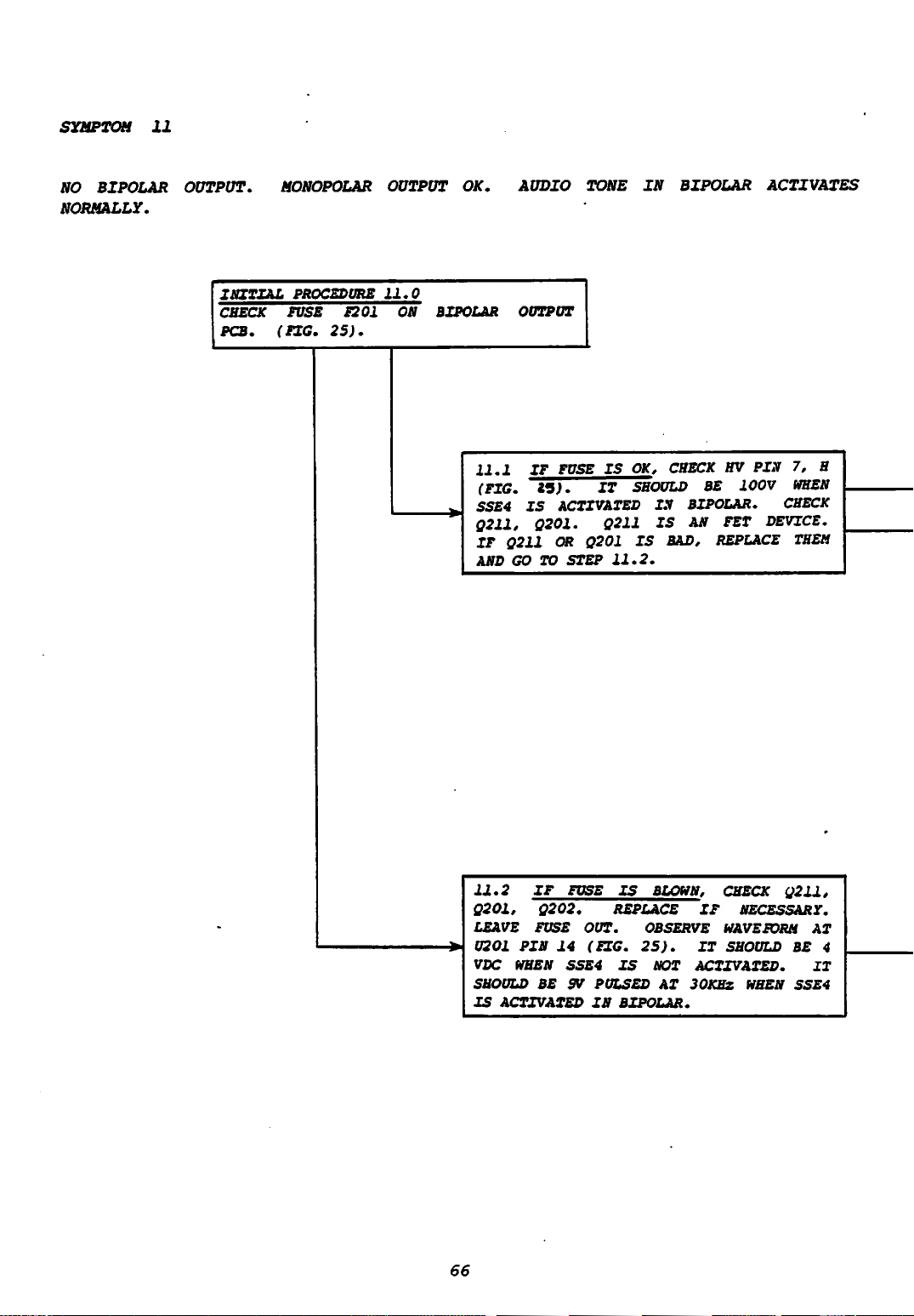
SYMPTOM
NO
BIPOLAR
NORMALLY.
11
OUTPUT.
MONOPOLAR
OUTPUT
OK.
AUDIO
TONE
IN
BIPOLAR
ACTIVATES
INITIAL
CHECK
PCB.
PROCEDURE
FUSE
(FIG.
25).
F201
11.0
ON
BIPOLAR
U.l
(FIG.
SSE4
OUTPUT
IF
V5).
IS
Q211, Q201. Q211
IF
Q2U
AND GO TO
FUSE
IS
IT
ACTIVATED
OR
Q201
STEP
11.2.
OK,
CHECK
SHOULD
IN
IS
IS
BAD,
HV
BE
100V
BIPOLAR.
AN
FET
REPLACE
PIN
CHECK
DEVICE.
7, H
WHEN
THEM
11.2
Q201, Q202.
LEAVE
U201
VDC
SHOULD
IS
ACTIVATED
66
IF
FUSE
PIN
WHEN
BE
14
FUSE
OUT.
SSE4
9V
REPLACE
(FIG.
PULSED
IN
IS
BLOWN,
OBSERVE
25).
IS
NOT
AT
BIPOLAR.
CHECK
IF
NECESSARY.
WAVEFORM
IT
SHOULD
ACTIVATED.
30KHZ
WHEN
Q211,
BE
SSE4
AT
4
IT
Page 70

11.11
PIN
IT
VATED.
IF
HV
IS
NOT
14
ON CLOCK/CONTROL PCB
SHOULD
ALSO
BE
HI
CHECK
WHEN
AT
U621.
100V,
BIPOLAR
CHECK DSE
(FIG.
29).
IS
ACTI
11.12
CHECK
25).
BIPOLAR
BIPOLAR
F201
SHOULD
lOOmS
ALSO
U.
OK,
BIPOLAR.
RESET
BOTH
AND
CHECK
21
REPLACE
IF
HV
IS
IS
OBSERVE
START
AFTER
PIN
IF
WAVEFORM
IF
IS
OK,
PIN
SIGNALS
NOT
ACTIVATED.
LOW
BIPOLAR
W
F201.
F201
Q211, Q201, Q202.
THRU
Q210
IF
Q211
CONTINUES TO
TO
FAIL,
GO TO
BLOW,
11.1.
Q211,
P
AND
KEY
Q201
PIN
SHOULD BE
ACTIVATED,
AFB
AND
GO
FOR6mHz
PIN
IS
LOW
REMOVE
16.
HIGH
ACTIVATED.
CLOCK.
AT U201 PIN
REACTIVATE SSE4 IN
FAILS
ALSO
WAS
AGAIN,
CHECK
BAD.
OR PARTS CONTINUE
ARE
OK,
T
(FIG.
HI
WHEN
WHEN
FUSE
AFB
WITHIN
14
RECHECK
Q207
IF
FUSE
IS
11.121
IF
RESET. KEY, CLOCK OR AFB
ARE INCORRECT, PROBLEM
BIPOLAR CONTROLLER
BIPOLAR
11.122
PCB
kHz
kHz
MODE. CHECK
SQUARE WAVE
CONTROLLER
IF
ALL
SIGNALS
ARE
OK,
CHECK
WAVEFORM, CHECK
ONLY
WHEN
ACTIVATED
Q211
WHEN
ACTIVATED
PCB.
U204
U203
GATE
IS
PCB.
FROM
PIN
PIN
PROBABLY
CONTROLLER
11
3 FOR
IN
FOR 8
IN
BIPOLAR.
IN
REPLACE
FOR
750
750
BIPOLAR
VOLTS
67
Page 71

ALL
WAVEFORMS
HORIZONTAL
VERTICAL
SEEN
ACROSS A
SENSITIVITY-lOus/cm
SENSITIVITY-500V/cm
300
OHM
LOAD
CUT @
300
SPRAY COAG @
116
W
W
FIGURE
MONOPOLAR OUTPUT WAVEFORMS
12
68
Page 72

!!!':;
.iniuiiiiBiaijiiiui
BLEND
1 @ 250 W
BLEND
BLEND 3 9
2 @
200
200
W
W
FIGURE
12
CONTINUED
69
Page 73

KEY MBP
Q211
GATE
2V/div
luS/div
SETTING
300 OHM LOAD
KEY
STD
- 40W
MBP
Q211 DRAIN
50V/div
luS/div
SETTING -40W
100 OHM LOAD
BIPOLAR
FIGURE
OUTPUT
70
13
WAVEFORMS
KEY
STD
MBP
RF OUTPUT
50V/div
luS/div
SETTING - 40W
100 OHM LOAD
Page 74

ov
am
KEY
STD
MBP
Q203 COLLECTOR
20V/div
20uS/div
SETTING -1W
100 OHM LOAD
KEY
STD
MBP
Q201 EMITTER
20V/div
20uS/div
SETTING
100
OHM
- 1W
LOAD
FIGURE
13
CONTINUED
UNKEYED
Q213 COLLECTOR
5V/div
5uS/div
Page 75

SIGNAL COLLECTOR CURRENT
OUTPUT
RED
KEY
CONTROL SETTING 58 WATTS
BOARD
WIRE
COAG
LOOP
(SEE
FIGURE
300 OHM LOAD
21)
SIGNAL
POWER
TEST
F2
(8
HV
SWITCHING
SUPPLY
CONTROLLER
POINT5(SEE
AMP)
REMOVED
FIGURE
BOARD
46)
FIGURE
TROUBLESHOOTING
72
SIGNAL
CLOCK/CONTROL BOARD
TEST
KEY PURE
14
WAVEFORMS
G
POINT
CUT
601
(SEE
FIGURE
30)
Page 76

O
KEY
BLEND
1
O
KEY
BLEND
2
.
•
si
—
--
-
J
HunaBEBB
+ i •
-r-4-
• + «
"r
bMB
5//S
••
-.'
.
^
i
-r-
1
•
1
•"
I
.
§SBBBBBB
BBBBEBB
O
KEY
BLEND
3
SIGNAL
CLOCK/CONTROL BOARD
TEST
(SEE
G
POINT 601
FIGURE
30)
O
KEY
SPRAY
COAG
"'
FIGURE
14
CONTINUED
73
Page 77

©a
KEY
PURE
CUT
Ob
KEY
PURE
CUT
SIGNAL T/ON
DRIVER
(SEE
BOARD PIN 10
FIGURE
34)
CONTROL SETTING 150 WATTS
300 OHM LOAD
SIGNAL
DRIVER
(SEE
FIGURE
T/OFF
BOARD
PIN
34)
9
SSE4
BIPOLAR
NOT
ACTIVATED
IN CUT, COAG, OR
SSE4 ACTIVATED
WITH RF OUTPUT
(ANY
MODE)
O
lV/div,
CPU BOARD U403, PIN 5
(SEE
FIGURE
LAMP
FIG.
14
ENABLE
.5mS/div
19)
CONTINUED
74
SSE4
WITH
(ANY
ACTIVATED
NO RF
OUTPUT
MODE)
Page 78

OV
©
KEY
COAG
©
KEY
PURE
CUT
SIGNAL COLLECTORS
STRIPLINE
KEY
IN FOOTSWITCH MODE
(SEE
CONTROL
BOARD
FIGURE
SETTING
35)
TERMINAL
E2
116W-OPEN
CIRCUIT
SIGNAL
STRIPLINE BOARD TERMINAL E2
KEY IN FOOTSWITCH MODE
CSEE
CONTROL SETTING 150W - 300 OHM LOAD
COLLECTORS
FIGURE
35)
FIGURE
14
CONTINUED
75
Page 79

SECTION
9
ASSEMBLIES
AND
SCHEMATICS
76
Page 80

ID
^
'W
R
CABLE
SUPPLY
POWER
Jp5*jT
v«¥:'
^
ii c
JiCcU]
MODULE
Mnr.i
imp
JHC5M
stripi
STRIPLINE
jlii(;4-J
v-y
/r\2''
JllGJ-j
/"
^
D C
tZI
(5)
MODULE
OUTPUT
< *
< ) £
vZ=D
CZZD
D
D
D C
2
<•
D
finMMn!=tHfrn;r=i?
»f > c
D
c:
CABLE
BD
SPEAKER
OUTPUT
BIP
CABLE
1
1
a
8
a
Co
5!
Page 81

£ZL
(5-
I/Ill
£3
ri.
T
-
\w
)
1)
a.
l V.
^
FIGURE
FORCE 4 COMPONENT/CONNECTOR
75
D
16
LOCATIONS-SIDE
VIEW
Page 82

PATIENT
E3-
=r
j
[wis"
ASSV
I
PW4
| |
MTERFACE PCI
piiz
I
3a—i
ASSY
CONTROLLERPCI
aOa/COHTROL PCI ASSY
•VOLAR
JMI
c«q—-
|
ASSV
PCI
ASSV
SENSE PCI
JMI
|
ASSV
KI
DRIVER
P"5!
ASSV
OUTPUT
TRANSFORMER
~1
ASSYS
ISREBTU
MODULE
ASSY
OUTPUT
nxn
MONOPOLAR
ACCESSORY BAHBSMICH
UCBOBIPOLAS DISPLAY
qo|
|o
oQ\
O
|Q
O?o]
PCSAUY
I-
DISPLAY
MONOPOLAR
J2I2
n
l~
BOARD
l£Y
MONOPOLAR
|
JMI
—|
PCI ASSV
OUTPUT
lOOmilPttAfl
PARENT
ASSV
PCI
CPU
|
-JWM
PCI ASSV SPEAIER
ASSY
PANEL
H^
J
|
|
Jllll
J1M2
|
Will
PIM21
-|
-|
I Jim
J1N3
P1M1
mooue
supply
poker
PCI ASSV OUTPUT
MODULE
•TRlPLtNEPCIASSY 6
T
J1H2
ASSY
RESISTOR
PCI
JS
STRIPLINE
©B
COMCCTORS
fOOTSWTCH
M©
L_
.J
CONTROLLER
ASSY
PCI
MODULE
SUPPLY
POWER
OYBOAfiO
mtaoetPQiAt
FRONT
ft
o
to
a
p
s
nj
bj
h-
§
fe
>
H
bl
o
o
CO
Nl
H
a;
s
g
&
Page 83

POWER
SUPPLY
PIN
J
i
2 HV GNO
3
u
5
6
7
8
9
10
11
12 -
13
♦
MONOPOLAR
FOOTSWITCH
J
PIN
i
0 GNO
2
3
SAMPLE
<t
5
DSCSPL
0 GNO
6
7
SPEAKER
PIN
J
v •"* ~
l
2
t.
3
/ - -
\ . " ! ,
4
3
o
1801
COLL
DISS
HV
HV CL
0 GNO
A GNO
♦
S V
READY
VS
IS
1803
FsTB
FSCT
DSC
1802
. -
:*•.;
BIPOLAR
OUTPUT
PIN
J
201
0 GNO
1
A
0 GNO
♦
2
♦
8
3
C
<4
0
5
c
SV
V
S
F
7
H
8
J
9
K
10
L
11
M
12
N
13
P
IX
R
15
S
16
T
17
U
18
V
19
H
20
X
21
Y
22
Z
23
AA
24
AB
25
AC
26
AO
HV
HV
HV GNO
HV GNO
RESET
OSE OSE
V
SEN
I
SEN
OC
AFB
KEY
SON
DSIE
0S2E
6 MHZ 6
LE
E CON
DSC
DSC
♦
1SV
♦
ISV
-
-
A
GNO
A GNO
5V
SV
OS
SEN
SPL
SV
5V
BIPOLAR
CONTROLLER
J
301
0 GNO
0 GNO
♦
5V
+
5V
OS
RESET
V
SEN
I
SEN
OC
SEN
AFB
KEY
SON
OS1E
0S2E
MHZ
LE
ECCN
♦
I5V
♦
ISV
-
5V
-
SV
A GNO
A GNO
CPU
J
0 GNO
0 GNO
♦
♦
ACC
ACC
VOL
VOL
FSCG
FSCT
READY
HSRYE
CTRYE CTRYE
CTE
OSE
CGE CGE
Bl
CPE
B3
ACRYE
CG2
CGI E
OSI
CS2
750
REM MODE
RTF
E
E CON
AUDIO
AUDIO
♦
♦
-
A GNO
A GNG A GNO A GNO
101
SV
SV
HSCG
HSUO
OS
HSCT
SS
E
KHZ
LE
REM
15V
ISV
SV
SV
CG
CT
1
2
E
E
E
E
1
2
FOOTSWITCH
J
CONTROL
501
0 GNO 0 GNO 0 GNO
0 GNO
♦
SV
*
SV
OS
FSCG
FSCT
HSRYE
SS SS
CTE CTE
HSRYE
OSE
Bl E 81 E
CPE
83
E
ACRYE
CG2
E
CGI E CGI E
OSI
E
0S2
E
7S0
KHZ
750
E CON
♦
ISV
♦
ISV
-
5V
-
5V
A GNO A GNO
ISO.
CLOCK
SENSE
J
601
0 GNO D GNO
♦
SV
♦
5V
J
♦
♦
CNO
OFT)
OS
CSCT
CSCG
CTRYE
S s"
OSE
CGE
CPE
J3
E
ACRYE
CG2
E
OSI
E
0S2
E
KHZ
E
CON
♦
ISV
♦
ISV
-
SV
-
SV
CSCT
CSCG
HSRYE
CTRYE
S3
COLL
COLL
E
♦
♦
-
A GNO
A GNO A GNO
CSH
CSH
CSL
CSL
OND
OFD
OS
CON
801
SV
SV
I5V
15V
SV
SV
DRIVER
J1001
0 GNO
0 GNO HV GNO
♦
♦
HV GNO
HV GNO
CSH
CSH
CSL
CSL
ONO
OFO
T OFF
T OFF
T ON
T ON T ON
HSRYE
CTRYE
STRY
CTRY
HVCL
E
HVCL
DISS
OISS
COLL
COLL
♦
♦
-
-
A GNO
15V
15V
SV
5V
SV
5V
STRIPLINE
'
J 1101
HV GNO
HV GNO
HV GNO
CSH
CSH
CSL
CSL
T
OFF
T
OFF
T ON •^C
HSRYE
A..
RYE
STRY
CTRY
HVCL
HVCL
COLL
COLL
HV
HV
♦
ISV
♦
ISV
-
SV
-
SV
INTERFACE
J 101
HS
CO
HS
C3
REM MODE
REM
MOOE F
ACC CG
&--C CG
HS
CT
HS
CT
HS
UO
HS UO
CT
-.:
CT
O GNO
O GND
O GND
D GNO
♦
ISV
♦
ISV
♦
15V
+
15V
-
SV
-
5V
-
SV
-
sv
♦
5V
♦
sv
♦
sv
♦
sv
LE
LE
RTF
RTF
COLL
COLL
E
REM
E
REM
A GNO
A GNO
A GNO
A GNO
PIN
i
A
2
8
3
C
•4
O
s
E
6
7
H
8
J
9
K
10
L
11
M
12
N
13
P
14
R
15
S
16
T
17
U
18
V
19
W
20
X
21
Y
22
Z
23
AA
24
AB
25
AC
26
AO
PCB
INTERCONNECT
FIGURE
18
LIST
80
Page 84

vo
S
bl
CO
Ci
vl~*=%.
r—-<^
<—-I
Page 85

CPU
FIGURE
SCHEMATIC
20
iu
£<
» » *
«r
9
o
5 s
O o
O
•>
O
8
9
o
s
o
8
O
3
o o o
353
s
S
CD
O
s
O
CD
3
CM
_ O
- -
- -
N
- —
-
—
K
XXX
Sod
CC
^
M
^
mi
Ml
Ml
<o
V
K
s,
•w
f-'
^
n
0>
«
ID
V
s
»«.
n n a
«»
K ^
M
<o
<0
0.
XXX
iu.
5»x
1-
<
CL
>
o
3:
-*
o
3
«o
o
CM
*~3
<<
lx
j
i
SO
3
o
o
fO
2
T
5
T
OB
r»
o
ace
^-3
CC
<f
lx
<fl
O
10
CB *
«4 S!
1
i i
->
T
'
X
-
-
7
3
5
o
n
K
Ml
i
A"5
<0
1x
_J
<r2J
xo«
X
or
XieS
5<
UJ
o
X
GD(
<
Ul
XS
u...
1
UJ
f/
Ul,
(dA
'^-<>He-<Hi«
Ul
uq
X-
Ul,
o
->
f
X
OC
X
s
i
<o
3
K
1
09
2
1
a*
l
o
5
4
'
s
ai
1
2
CM
o
1
i
m
4
at
I
S
1
1
1
o
2
s
1 i
I
CM
CM
X
1
CM
CM
I
ill
CM CM CM
»*> v
1 1 1
ui
CM CM CM
«X) •*•
Sea:
4 4 4
1 1 1
X
0
J)
0»
CM
2
o
2
1
s
lO
1
lO
lO
2
1
2
1
4
X
a:
MJ
4
v0
1
S 2 S
* * 2
p» a> cji
»o
l 1 l
Ml K>
«Jt<3
o
U
3
5
3
3
3
CI
3
3
o
3
3 ;
5 3
5 3
w
u
s
cfuj
o
X
(01
4I<
<0
10
O
w
4
o
<0
O
4
lO
s
(0
o
•a
o
to
<0
o
«0
o
<0
O
•
O
o
•r
O
4
K
e
5 S
> o
r *
• s
0
CD
CD
O
4
o
CD
O
4
>r
5
*
*
K
l<
2
X*
1
Ul,
.u.,,
in
+
OAo^»o
>2|
i
-oH(-<H|i
•Oit^l-
o
o
l
1
i
o
2
3
I
2.
o
1
*>
10
1
Ul
2
1 i
i
i
'
1
X
!
2
'
X
1
1
T
o
3
3
7
i
a
i
s
T
3
2
T
o
a
I 7 1
4
2
i
c
1
2
C
>
- £
Li
i
at
2 :
3 :
i
c
: >
M
i
S
7
tr
4
CC
CM
o
4
o
1
2
X
1
O
CM
Ml
*•
->
2
1
5
1
o
to
0.
1-
o
<
-J
>»
X*
,<P
aX
"3
fflj
«•
->
JLx
tr-;
Ix
CD
+
CD,
«
~3
"3
X
SCO
X
-
-
•
- -
-
•
9
0.
o
s
O
e
IM
«>
S
•
a C
n »
* <
— c
3 C9
M —
CM
o
«
o
«r
a
»
x
-
- -
^
Ml
K
<o
\
ID
-
m
1
-
\\
« r
* «>
Ljl
- •
.
ID
Ml
^
fw
*
Ml
X
X
X
5
s
1
2
s
S
ii
at
cr
c
K
K
z
>
3
5
i
3
5
<S|«M
<D
CD
2
-
*.
co
mi
A
O
e-
.M
-
2
* *
Ml
Ml
mi
a
mi
o
»
<0
<o
2
0
«
2
§
\ /
/
\
/
5
? i *
M C
2
CM
5
s
<D
CM
X
X
co
X
X
s
X
X
X
X
£p
s
'
<
^
^ x
^
S
/^
^
S
^
•^
y
^
V
,^
V
y
v
^
s-
o
X
^
5
3
5
4
<r
u
4
o
w
o
4
5
3
U
5
4
u
5
3
V
9
4
o
M
3
O
O
4
«r
y
O
4
<»
u
M
4
u
o
M
^"
4
o
w
Ml
5
O
u
4
4 4 4
5 * *
tt
o o o
o w o
m
ft
3 2 5
to
o o —
o 0 o
*>
O
4
s
u
U
3
4
3
O
s
4
3
S
X X *
* Ml M
*
O U O
» » v
«r
C X
*
IV
a
O
CM
3
«r
n«
o
=
CM
1
o
1
i
^
V
s
3
S
r*
~
i
in
i
i
i
to
3
i
<o
i/>
i
i
0*
o
1
'
3
3
. *
1
5?
o
o
i
CM CM CM
ff> O N
1 1 •
\o
(M CM <M
1 1 •
«n
«
CM
o
to
CM .
CM
1
M)
i
1 1 '
1
2
X
X *
C X •
7
*
1 1
10
CM
1
CCS
1
Page 86

. i
I
!»?•«!*
Tn
rrrlV
•i
nix*ns'Jia»i
OJ
ll.-lt
!.b;dnrN
Hid
ON*
1|
i— »-» u 4-» - i
i,.-2A5x I
>lT
Jil
^••••^•••••"V-i
^;-,.;..-^^lJ
8
to
CO
8
soa
ssmcxm
oi
Page 87

FIGURE
21
OUTPUT
BOARD
84
Page 88

CLAMP
MR826
CR3
SELECT
OUTPUT
•>
C3
I80PF
-H(-
3300PF
J_C4
1
CR2
SPARE
->
AII5M
T
-> H.V.
SPARE
•>
CI
;0.luf
-> ANTI SAT.
H
CRI
MR8I6/AII5M/S6F
600V
8
->GND
10
BASE
->
PROBE
CURRENT
±\>
Ql
FESEI78
UTR-
CR4
.fAll5M/
560PF
C2
ft
4360
bj
§
Rl
0.1 A
-vw
>•
>
to
> >
8
8
Page 89

Ml
n n n n n
law
it~~icriii
I RI53 I
H
CI27 Q
CI3I O
icniw
CI28
| I
ens
IR73T1
IwTSFl
innnr
I
OCI26
>CI29
<=>
C130
cTc-S
CRI06
o
•o
5
RAIOI
faTgsl
©••
to
[Ri44l
im5n
>Ri4n
o
5
<M
Cjg3
gTSlJ
sp
n=
§|
1
o
•o
5
to
>CI04
0104
,
OOcTO-os
OCI42
CTXI43
OCI2S
<=>CI23
OCI4I
fa
§21
CI06<
UOUUUU
OIOSV-^.^
0106
RTgg
CRI09
Jg5S
<^5CI44
CMS
^-\
OIQIfIL_j0'02
RTS7
RTS4
CRI03I
1CRI04
CI24
CM 7
SEE
hTSS
ML
/-N
CRIIO
CI40
rp:
IgS
CRIOS
CRIOft
IffTTT.
5i2o"
CO
CIO
FIGURE
INTERFACE
]
12
23
BOARD
86
B
Page 90

H—=L
INTERFACE
FIGURE
BOARD
24
SCHEMATIC
o
5«
*T*=I
10
oc
o*t
gSrf'
cjg
Page 91

FIGURE
25
BIPOLAR
OUTPUT
88
BOARD
Page 92

imodisotam
I I 4
11
I
IO-WV
' n *•
7°5^
~s
51-i
39
55
t * *-»
—II
HIll«-
SS
l
It—
55sH"
^npQP^0^!
|—vCvkQh>
??
v v
U>U
I
III!
v"
CN*(D
v
•»<
BIPOLAR
f
FIGURE
OUTPUT
BOARD
89
JJ
26
SCHEMATIC
U0O
Page 93

0?
+ °
w*»
CR302
C309
3|
.1——1,-^
^CD|.<*
C306 C305
Jo
C30I
IR3271
Id
so
so
OS
ft*
(EH
^201
ESS
R3U
3E
UL£
41&
RTT7
ffjtl
gSSl
O
;3»
<£52fo
v
'Ml
C32I
C3I6
C3I3
[K3TS1
O
D
C3I4
alia
0
ESI]
IRJ>j>al
•Ri^9l
(R33T1
1^3731
IK3351
C304
C302
C303
C3>~
CR303
CR304
CR30S
CR306
>m
BIPOLAR
FIGURE
CONTROLLER
27
SO
BOARD
Page 94

FIGURE
! a 2
28
BIPOLAR
CONTROLLER
BOARD
91
SCHEMATIC
Page 95

FIGURE
29
CLOCK/CONTROL
92
BOARD
Page 96

to
o
o
a
P4
8
3
O
iii^ji^
T%^gi::J
|L
Bmj-u
fc^,
f^ew
j-^.^
fL^j
Lm
Ifa^J
Page 97

FIGURE
31
SENSE
BOARD
94
Page 98

8"
*n
i
SENSE
FIGURE
BOARD
32
SCHEMATIC
95
Page 99

5
tr
I
FIGURE
DRIVER
cm
O
S
33
BOARD
0
o
CM
CM
o
O
5
£
• CM
CM
o
£
96
Page 100

J1001
-CM*
I
° bj
i §
si
8
 Loading...