

Page 1

Force
Service
Force
Force
30
40
Manual
Valleylab
5920
Boulder,
For
Copyright © Valleylab
All
permission
Longbow
Colorado
service
rights
Inc
Drive,
80301
information
reserved.
Valleylab
of
P.O.
Contents
Box
9015
USA
1-800-255-8522
call:
Inc,
1992
of
Inc.
publication
this
1-303-530-2300
/
be
not
may
TWX
/
reproduced
910-940-2514
form
any
in
without
the
written
Page 2

Foreword
The
following
equipment
service
described
instructions
in
this
manual.
are
for
use only
by
personnel
qualified
to
repair
and
service
the
Caution:
Federal
Effective
Equipment
REM"
is a trademark
PolyHesive®
Purpose
This
Service
the
Force
30
generator
The
Limited
Valleylab
use
and
replacement,
applicable
to
Valleylab’s
has
been
reliability,
and
reader
Warranty
Inc
service
time
repaired
or
(USA)
Date:
April
covered
in
is a registered
And
Scope
Manual
and
contains
Force
cautions
is
directed
warrants
at
satisfaction,
which
for
the
its
sole
period
or
altered
has
each
period(s)
option,
shown
that
been
law
restricts
1992
this
manual:
of
Valleylab
trademark
information
40
Electrosurgical
and
warnings
to
the
Force 30,40
product
outside
manufactured
set
forth
of
any
product,
below
after
the
product
Valleylab’s
subjected
below.
delivery
to
misuse,
this
device
Valleylab
Force
Inc
of
Valleylab
required
Generators.
concerning
Instruction
by
Valleylab’s
or
part
thereof,
of
the
is
defective.
factory
neglect
to
sale
Part
No.:
30,
40
110 — 120
220 — 240
(user
selected)
Inc
to
electrosurgery
it
to
be
free
obligation
which
product
This
in a way
warranty
or
accident.
to
so
by
or
on
the
945
100
153
Electrosurgical
V-
nominal
V-
nominal
calibrate,
troubleshoot,
Instructions
are
Manual
from
the
as,
defects
under
has
been
original
does
in
Valleylab’s
supplied
in
this
returned
purchaser,
not
apply
order
Generators
for
the
beyond
with
material
warranty
to
to
any
judgment,
of a physician.
maintain,
operation
the
the
and
workmanship
is
limited
it
or
its
and
which
product,
to
of
scope
of
generator.
to
the
Distributor
examination
or
part
affect
its
and
install
the
Force
this
manual.
under
repair
or
within
discloses,
thereof,
stability
normal
the
which
or
The
warranty
Electrosurgical
Mounting
Footswitches
Patient
Sterile
This
warranty
merchantability
Valleylab
use
of
Valleylab's
price
for
disclaims
damages.
This
warranty
Colorado,
Court
Valleylab
any
time
them.
periods
Fixtures
(All
Return
Disposables
neither
any
of
Valleylab's
liability
the
goods
any
liability
USA.
for
the
County
Inc,
its
without
for
Generators
(All
Models)
Models)
Electrodes
is
in
lieu
and
fitness
assumes
with
sold by
hereunder
and
the
rights
The
sole
of
dealers
incurring
Valleylab’s
of
all
other
for a particular
nor
authorizes
products.
respect
Valleylab
forum
Boulder,
and
Notwithstanding
to
this
or
and
obligations
for
State
representatives,
any
obligation
products
One
One
One Year
Shelf
Sterility
warranties,
purpose,
any
agreement
to
customer.
elsewhere
hereunder
resolving
of
Colorado.
to
disputes
make
are
as
follows:
Year
Year
life
only,
only,
expressed
other
person
any
and
There
in
connection
reserve
the
from
date
from
date
from
date
as
as
or
and
of
other
products
are
shal]
arising
the
right
same
of
of
of
stated
stated
implied,
all
other
to
assume
provision
sold
no
warranties
with
be
construed
under
to
or
similar
shipment.
shipment.
shipment.
on
packaging.
on
packaging.
including,
obligations
for
it
herein
hereunder
the
sale
or
relating
make
changes
changes
any
which
of
this
under
without
or
liabilities
other
liability
or
in
any
shall
be
extend
product,
and
in
any
in
equipment
on
equipment
limitation,
on
in
other
limited
beyond
for
indirect
governed
way
to
this
previously
the
the
part
connection
document
to
the
aggregate
the
terms
or
by
the
warranty
built
and/or
warranties
of
or
hereof.
consequential
laws
sold
built
of
Valleylab.
with
the
communication,
purchase
Valleylab
of
the
State
is
the
District
by
them
and/or
sale
sold
or
of
at
by
Page 3

Table
Section
Responsibility
Environmental
Transport
A
Preparing
Power
Power
Proper
Preoperational
Routine
Cleaning
Recommended
Reusable
Reprocessing
Cleaning
Ethylene
Steam
Section
Output
Low
High
REM
Audio
Input
Weight
Overall
Classification
Class
Type
Defibrillator-Proof
Drip
Intermittent
Force
Force
Force
Force
of
Contents
Installation
1
of
Conditions
Storage
and
eeeeeeereerererere
Generator
the
Requirements
....................................
Plug
Grounding
Checkout
Maintenance
Instructions
Electrosurgical
Pencil
に
Oxide
Autoclave
Performance
2
Configuration
Frequency
Frequency
Contact
Volume
Power
CF
Proof
30
30
40
40
Quality
Source
...................................4...
Dimensions
..................................
Equipment
I
Equipment
per
Operation
Output
Output
Output
Output
.................
Manufacturer
the
.......................
.................................
Use
for
............................
..............................
........................
Inspections
and
...........................
Cleaning
Directions
に に
に
に
に
(EtO)
Processing
and
トト
ーー
Processing
......................
ドド
ドー
に
............................
................
..................
..............
Accessories
トー
ドド
トド
ドド
トド
........................
..........
ドド ドド
ドー
Specifications
...........................
...............
Leakage
Risk
.................................
IEC
Waveform
Characteristics
Waveform
Characteristics
(50-60
Parameters
Monitor
.............................
.............................
IEC
per
IEC
per
...................................
601-1
.................................
Hz)
.................
....................
601-1
.......................
......................
601-1
.............................
......................
..................
......................
.......-..........
ыыы
DNA
ND
ο
ババ
DBA
RB
nA
.
JIA
00
00
00
00 00
00
00
00
00
LO
LO
Page 4

Functional
Section
Overview
Microcontroller
Microcontroller
Serial
Footswitch
Watchdog
Voltage
Display
7-Segment
LED
REMLamp
¡11
Front
REMSwitch
Power
Voltage
Interface
¡AS
Handswitch
RF
Dosage
RF
REM
Voltage
REM
Power
AC
LVDC
HVDC
ЕСОМ
Dosage
Ton
Clamp
Load
3
.......
Communication
Decoding
Timer
Regulators
Board
LEDS
Lamps
LO
Sense
Sense / Dosage
Filter
Supply/RF
Line
Generation
.........................................
......
Buttons
Panel
.................
Control
Regulators
Board
Key
........,.........,........................
Error
........................................
Circuitry
Regulators
Board
Hardware
Power
Supply
Power
Supply
Error
........................................
Signals
Enable
........................................
이
κ
レト
기이
기
εν
トト
οκ
0
.....
이아
이이
이기
καν
トー
レイ
ersnsee
κνν
ーー
Description
이기기
기
이기기
기
Board
/
................,................
Pencil
.......................................
...........................
.........................
Memory
.....................................
....................................
................................
Sense
νεο
Board
.....................,................
/1/O
....................
Bus
IIC
the
on
.................................
...................................
0000
..................................
eee
.
Detector
...................................
Error
...................................
..............................
...................................
.................................
................,................
..........................
................................
Gain
Test
......................
κκ < スー
ドド
トド
ドド ・ ト
トレ
.........................
23
23
23
23
24
25
25
26
26
26
26
27
27
27
28
28
28
29
29
29
30
31
32
33
34
34
RFOUutputStage
Voltage
Regulators
.......................
...................................
000.010
e
Page 5

Controls,
Descriptions
Section
Indicators,
Introduction
Status.............
Power
Bipolar
Monopolar
Monopolar
Alarms
Front
Rear
4
and
.......................,...........
Controls
.......................................
...........
Panel
Panel
.........................,.......
.................................
Cut
Coag................................
Receptacles
Functions
Receptacles
0s
...........................
Of
........
게
이
rr
.........................
시
에
사
43
43
47
47
48
48
48
49
50
51
Section
Recommended
General
Pretest
Front
Rear
Chassis
Power
Calibration
General
Setting
Multiplier
REM
Calibration
Summary
Error
5
Test
Inspection
Panel
Panel
Inspection
Self-Test
Up
Instructions
Up
Offset
Filter
Table
Codes
Section
Section
Returning
Returning
Returning
Ordering
7
Calibration
Testing
Test
And
................................ss..sse
....................................
Calibration
for
Calibration
Board
Steps
of
...................................
Component
6
Factory
Generator
the
Force
the
Circuit
Replacement
And
Equipment
Calibration
..............................
....................................
.............................
.....................,............
Calibration
...............................
Calibration
the
...................
Information
νεο
ρο
νοκ
ω
.......................
.....................
....................
Steps
Replacement
............
...............
....................
Subassemblies
40
30,
Boards
Parts
Service
Service
for
Generator
Other
and
............................
.....
..........
κ
οσον
εοσ
...........
εκν
εκ
κοκ
て
....
.........
53
53
54
54
54
55
55
55
56
56
57
57
57
58
62
63
67
69
69
69
69
69
Service
Section
Display
Interface
Microprocessor
Power
REM
Section
Electronic
Cable
Connector
8
PCBA
PCBA
Supply
filter
9
Interface
1:
#
PCBA
Assemblies
Low
#1:
Parts
.................................
................................
PCBA
PCBA
...........................
............................
..............................
List
and
Between
Voltage
Microcontroller
Boards
Interconnect
Board
..........
Schematics
...............
...............
Cable
Board
PSRF
to
..
.......
71
71
72
75
76
80
81
81
81
82
Page 6

List
Figure
Figure
Figure
Figure
Figure
Figure
Figure
Figure
Figure
Figure
Figure
2.1
2.2
2.3
3.1
4.1
4.2
4.3
9.1
9.2
9.3
9.4
of
Figures
Force
Force
Output
Functional
Force
Force
Rear
System
Interface
Power
Display
40
Output
30
Output
Power
40
30
Panel
Supply/RF
vs
Block
Front
Front
..............
Interconnect
Schematic
Board
Power
Power
Panel
Panel
Schematic
vs
vs
Generator
Diagram
......
......
Diagram
.......
Schematic
Load
Load
Setting
..
e...
..........
ecos
...........
e.
............
..
.
.........
.........
......
cs 0 0.
11
15
18
41
45
46
83
84
88
92
Figure
Figure
9.5
Microcontroller
9.6
REM
Filter
Board
Board
Schematic
Schematic
........
ss...
95
97
Page 7

Service
Valleylab
Boulder,
800-255-8522
Valleylab
Stamford,
800-843-2872
Valleylab
Prospect,
61-2-688-4888
Valleylab
Nieuwegein,
31-3402-32456
Valleylab
Ontario,
800-668-1832
Valleylab
London,
44-081-961-9956
inc
Colorado,
Inc
Connecticut,
Australia
AUSTRALIA
Benelux
HOLLAND
Canada
CANADA
Europe,
UNITED
Centers
USA
USA
Middle
KINGDOM
East
and
Africa
ATTENTION:
REFER
TO
ACCOMPANYING
DOCUMENTS
THE
Valleylab
c/o
Lyon,
33—78—096262
Valleylab
Wichmannstrasse
Postfach
D-2000
GERMANY
0049-4089-
Valleylab
London,
CLIMO
FRANCE
France
Germany
520452
Hamburg
6884
UK
UNITED
4
52
KINGDOM
44-081-961-9956
IO
TYPE
CF
LOW
LEAKAGE
SUITABLE
DEFIBRILLATOR-PROOF
EQUIPMENT
FOR
CARDIAC
USE
à
DRIP-PROOF
F
THE
HIGH-FREQUENCY
GENERATOR
PER
IEC
601-2-2
IS
ISOLATED
Page 8

Introduction
Force
The
models
feature).
All
convert
The
available
Note:
available
generators
the
differences
“-”
Force
and
30
this
in
configured
are
generator
between
functions.
indicates
the
Electrosurgical
40
Force
to
110-120
to
two
the
These
differences
mode
is
Mode
Pure
Cut
Blend
Blend
Desiccate
Fulgurate
Spray
Standard
Precise
series
operate
V-
major
not
available
Maximum
1
2
Coag
Bipolar
Bipolar
Generators
Force
are:
220-240
at
operation.
models
are
summarized
on
Power
30,
are
that
designed
are
the
and
40,
Force
nominal.
V~
maximum
the
in
the
particular
Setting
Force
300 300
250
200
200
150
150
50 50
50 50
A
power
following
model.
(watts)
40
ceiling
for
Force
kit
or
40S
available
is
settings
tables.
Force
30
250
一
200
150
一
mounting.
cart
(Simutaneous
Valleylab
from
number
the
and
The
Coag
to
of
40
30,
Force
The
and
panel
touch
a
contains
a
contains
panel
receptacles,
rear
The
potentiometer,
Feature
Handswitching
Footswitching
Simultaneous
Isolated
Power
Autoranging
Blend
Spray
generators
membrane
monopolar
the
handle,
and
Outputs
Control
REM
2
Coag
enclosed
are
switches,
footswitch
power
entry
monopolar
Features
Outputs
Output
Coag
the
in
lighted
receptacle.
module,
bipolar
and
Force
2
yes
option
yes yes
yes
yes yes
yes
yes
metal
same
indicators,
voltage
line
a
footswitch
40
molded
and
digital
displays,
selector
receptacles.
Force
30
2
yes
一
yes
一
一
plastic
high
switch,
enclosure.
voltage
volume
a
control
front
The
output
vi
Page 9

Section
Notify
returns
authorization
Carefully
cartons
service.
If
Valleylab
—
Valleylab
must
and
have
you
1-800-255-8522
Responsibility
only
if:
assembly
©
persons
electrical
the
—
as
IEC
—
the
equipment
1
to
have
number
remove
packing
questions
any
or
responsible
is
Inc
operations,
authorized
installation
and
BSI.
Installation
arrange
the
the
your
is
for
approval
be
must
generator
Force
materials
concerning
Valleylab
of
the
for
extensions,
by
Valleylab
of
used
in
accordance
replacement
repair
displayed
to
or
Valleylab
the
from
the
on
all
and
transporting
when
use
contents,
the
representative.
package
accessories
Manufacturer
safety,
the
the
effects
on
readjustments,
Inc.
with
room
the
relevant
parts
any
of
Customer
contact
reliability
modifications
complies
instructions
Service
label.
from
generator
the
Valleylab
with
damaged
shipping
the
performance
and
or
local
for
use.
from
Department.
package.
when
or
Customer
repairs
codes
Service
are
and
shipping.
return
The
all
Save
returning
the
of
carried
requirements
it
at
equipment
out
All
for
by
such
Environmental
Transport
Ambient
Relative
Atmospheric
and
Temperature:
Humidity:
Pressure:
Operation
Ambient
Relative
Atmospheric
Preparing
The
installed
hospital
Provide
cooling.
be
Temperature:
Humidity:
Pressure:
the
electrosurgical
ceiling
a
in
procedures
least
at
Under
warm.
DANGER
Explosion
anesthetics,
Conditions
Storage
Between
Between
Between
Between
Between
Between
Generator
generator
mount
local
or
six
to
four
continuous
Hazard.
gases,
Do
liquids,
10%
30%
may
system.
codes
inches
for
use
install
not
or
—40
and
and
100%,
500
and
+10
and
and
75%,
700
and
for
placed
be
is
It
detailed
for
space
of
extended
the
objects.
+70
degrees
noncondensing.
1060
millibar.
+40
degrees
noncondensing.
1060
millibar.
Use
mounting
a
on
recommended
information.
around
electrosurgical
the
periods
of
C.
C.
that
sides
time,
generator
(available
cart
carts
top
and
normal
is
it
have
of
in
the
Valleylab)
from
conductive
generator
top
the
for
using
areas
or
wheels.
for
and
flammable
Refer
convection
rear
be
panel
to
to
Force
30,
40
Service
Manual
1
Page 10

Power
The
280
50-60
Power
The
your
if
different
The
using
periodically
pull
Proper
important
An
grounding.
dangerous
failure.
Requirements
30,
Force
50-60
V~,
Hz.
Plug
generator
Force
country
from
connector
extension
the
cord
on
Grounding
currents
Electrosurgical
40
The
Hz.
is
equip
will
that
supplied.
meets
inspected
consideration
The
all
or
cords
by
itself.
ground
will
Generator
output
shipped
your
will
with
Valleylab
requirements
three-prong
assuring
the
in
the
from
personnel.
qualified
in
wire
flow
remain
hospital
a
generator
for
two-prong
to
patient
power
cabinet
designed
is
constant
grade
grounding.
safe
Cords
safety
is
cable
of
to
over
power
the
with
adapters.
should
while
connected
generator
the
operate
ranges
the
plug.
proper
purpose
Its
The
always
using
the
to
in
between
90-135
of
Valleylab
The
connector
should
power
the
cord
grasped
be
electrical
chassis
event
140
—
85
or
V~
representative
your
for
be
not
assembly
the
by
equipment
insures
and
internal
an
of
170
or
V~
180-270
operating
defeated
should
Do
plug.
proper
is
no
that
electrical
-
~,
V
in
room,
by
be
not
Hz
Undesirable
power
the
power
Preoperational
Refer
to
Routine
Valleylab
This
year.
procedures.
supply
Cleaning
Clean
the
clean
alcohol,
50-60
generator.
the
to
outlets
Section
5,
Maintenance
recommends
Service
major
For
any
parts
Instructions
generator
the
generator
caustic,
corrosive,
furnishing
Power
Manual
or
information
leakage
the
is
It
power
Checkout
Up
Self-Test.
the
that
describes
repairs,
standard
using
keyboard
cover,
abrasive
or
currents
responsibility
and
Force
the
needed
are
to
the
Force
Inspections
generator
recommended
the
generator
to
repair
hospital
cord.
and
cleaning
affected
also
user
the
of
generator.
inspected
be
returned
be
can
the
Force
procedures.
not
Do
materials.
polarization
the
by
assure
to
by
inspection,
to
generator.
a
Use
fluids
allow
generator
The
proper
gualified
testing,
Valleylab.
mild
to
service
detergent
enter
cannot
input
the
of
grounding
personnel
calibration
and
desired,
If
and
chassis.
the
be
50-60
polarity
and
twice
Valleylab
cloth
damp
use
not
Do
sterilized.
Hz
in
a
will
to
2
Force
30,
Service
40
Manual
Page 11

Recommended
Valleylab
Valleylab
Valleylab
Valleylab
Valleylab
Valleylab
Valleylab
Valleylab
E7507/E7509
E2515/E2516
E2525
E2517
Bipolar
E2400
E6008B
E6009
Electrosurgical
REM
PolyHesive
Disposable
Reusable
Disposable
Forceps
Disposable
Monopolar
Bipolar
Handswitching
Power
Insulating
Footswitch
Footswitch
Accessories
II
Patient
Handswitching
Pencil
Control
Pencil
Holster
Return
Pencil
Electrode
|
Force
30,
40
Service
Manual
Page 12

Reusable
(For
Valleylab
NOTE
These
Refer
Cleaning
pencil
The
1.
electronic
disposable
a
If
2.
matter
cleaning
pencil
3.
Dry
Sterilize
4.
autoclave
Ethylene
Coil
1.
wrapping
(blood,
with
thoroughly.
the
Pencil
Reusable
directions
to
the
should
components.
solution
a
the
sterilization,
Oxide
cord
of
are
instructions
be
electrode
mucus,
or
water-dampened
using
pencil
(EtO)
loosely
cord
the
Cleaning
Handswitching
intended
not
provided
processed
has
tissue)
blood
following
Processing
prior
will
with
been
by
dissolving
cloth.
standard
inserting
to
decrease
And
used
wiping
the
Reprocessing
electrosurgical
for
by
the
manufacturer.
delicate
other
the
in
the
detergent.
not
Do
hospital
handling
pencil
the
the
useful
Pencils)
accessories
surgical
pencil,
entire
immerse
procedures
life
remove
pencil
Remove
the
for
recommendations
EtO
an
into
pencil.
the
of
Directions
not
instruments
discard.
and
cloth
a
with
cleansing
any
pencil
in
Ethylene
below.
pouch.
manufactured
order
in
Remove
pad
gauze
or
agents
reprocessing
Oxide
Tight
by
sterilization
“bunching”
Valleylab.
by
gross
mild
a
the
steam
or
or
the
protect
to
all
and
wiping
solutions.
2.
Estimated
Steam
1.
2.
3.
4.
5.
Recommended
Autoclave
Do
not
the
Lay
the
Fold
lengthwise
NOTE
Keep
the
pencil.
Apply
a
autoclave.
not
Do
will
be
number
autoclave
pencil
the
exceed
reduced
body
material
(Fig.
.
pencil
Do
second
wrapping
a
when
wrapping
not
of
uses
when
Processing
the
pencil
center
the
in
pencil
the
over
2)
dord
body,
use
rubber
material
processing
this
product
procedure
reprocessed
unwrapped.
the
of
body
connector
plug
and
bands,
temperature
for
string,
the
to
is
steam
normal
by
wrapping
proceed
and
or
tape
packet
135°C
of
autoclaved.
autoclaving:
11
this
method:
material
coil
to
contacting
from
to
produced
(275°F
as
the
secure
in
for
)
20
shown.
cord
each
the
cord.
Step
minutes.
20
(Fig.
around
other
above
2
1)
material
the
prolong
to
(Fig.
The
the
Tape
3).
number
of
life
and
uses
of
4
r:
[|
|
2
7
Fig.
1
k
Fig.
2
T
Force
30,
KR
Fig.
Service
40
3
Manual
Page 13

Testing
During
Insert
1.
The
surgical
pencil
the
patient
procedure
connector
return
electrode
set
up,
into
must
inspect
appropriate
the
be
product
in
place
and
active
on
the
confirm
handswitch
patient.
product
function.
receptacle
on
generator.
the
the
Using
2.
generator
The
3.
Reset
button.
CAUTION
Set
NOTE
Observe
tone
the
Press
4.
illuminates.
Press
5.
illuminates.
NOTE
either
If
CAUTION
Inspect
damaged,
electrical
generator
and
Cut
the
sounds,
yellow
blue
the
the
the
shock
front
conduct
will
power
Coag
generator.
indicates
this
Cut
blue
the
If
Coag
yellow
the
If
Coag
or
Cut
and
pencil
use.
not
do
to
the
panel
settings
If
button
Coag
button
Cut
lamp
cord
Failure
patient
On/Off
self-test
a
error
an
malfunctioning
a
on
lamp
on
lamp
does
for
or
and
the
to
code
pencil
the
illuminates,
pencil
the
illuminates,
not
breaks,
observe
to
operating
the
switch,
lowest
(119-122) appears
illuminate,
cracks,
turn
power
and
and
settings
setting
accessory.
verify
discard
verify
discard
nicks,
precaution
this
room
personnel.
before
that
that
discard
or
generator
display
will
testing
the
in
the
pencil.
blue
the
pencil.
the
damage
with
the
yellow
pencil.
every
Discard
the
the
other
On.
1
the
power
pencil.
lamp
lamp
before
use
Do
watt.
pencil.
INES
setting
the
in
the
in
use.
result
may
press
not
displays
mode
Cut
mode
Coag
If
injury
in
and
the
a
or
6.
Place
Force
30,
the
generator
Service
40
in
the
Manual
Off
mode
until
ready
for
surgery.
5
Page 14

Force
30,
40
Service
Manual
Page 15

Section 2 Performance
Specifications
Section,
this
In
temperature
Output
Isolated
Low
All
Source
Normal
Normal
Reverse
Frequency
patient-connected
High
are
subject
"typical"
(25°
C)
and
Configuration
output.
Leakage
terminals
Current
Frequency
Polarity
Risk
to
change
to
refers
nominal
Ground
intact
open
open
Parameters
without
specification
a
input
power
(50-60
tied
together:
Leakage
Specifications
notice.
of
20%
is
that
voltage.
Hz)
Leakage
10µΑ
«
pA
100
<
pA
100
<
within
+
(110-120V~)
stated
a
Leakage
<2.0
50
<
<50
value
нА
pA
pA
room
at
(220-240V-)
Monopolar
Bipolar
REM
Measurement
Frequency
70
If
REM
resistance,
+ 5 kHz
impedance
the
mode,
RF
Contact
Audio
audio
The
Keying
Alarm
Tone
Tone
RF
leakage
leakage
measured
resistance
if
alarm
an
Volume
keying
(Fixed)
current
current
Quality
Measurement
Current
<
10
mA
is
increases
be
will
adjustable.
are
tones
Audio
45
>
Monitor
outside
generated.
to>
65
the
more
by
Level @ 1
65
dBA
<
150
mA
<
50
mA
Acceptable
Single
<
20
acceptance
than
alarm
The
dBA
RMS
RMS
ohms
40%
meter
area
range,
above
tones
Resistance
pad
REM
a
nominal
the
adjustable.
not
are
Dual
5
—
fault
Range
area
135
ohms
condition
value
pad
or
will
135
occur.
ohms
In
the
Force
30,
Service
40
Manual
7
Page 16

Input
Nominal
Regulation
Operating
Current:
Power
Voltage:
Voltage
Range:
Idle
Cut
Coag
Bipolar
Source
Weight
20
Ib
(9.1
kg)
Overall
7.8
in. H x
Classification
Class I Equipment
Protection
protective
basic
Dimensions
16.lin. W x
against
conductor
earth
insulation.
110-120
90-135
85-140
0.4
A,
7.0
A,
4.0
A,
2.0
A,
11.9
per
IEC
electric
shock
in
RMS
V
V
RMS
RMS
V
max
max
max
max
in. D (199
601-1
provided
is
way
a
such
or
or
or
.or
or
or
or
mm x 409
by
they
that
mm x 303
connection
cannot
220-240
180-270
170-280
0.2
A,
max
3.5
A,
max
2.0
A,
max
1.0
A,
max
mm)
accessible
of
become
RMS
V
V
RMS
RMS
V
live
in
conductive
event
the
parts
failure
a
of
to
the
of
Type
CF
Equipment
30,40
Force
The
allowable
used
be
Defibrillator-Proof
The
discharge.
Drip
The
generator’s
Intermittent
The
conditions
seconds
30
30,40
temperatures.
leakage
the
on
can
electrode
per
30,40
safe
Operation
(Pure
off
used
be
neutral
Proof
Force
generator
per
provides
currents
heart.
IEC
601-1
enclosure
and
satisfactory
cooled
is
Cut,
operation
for
IEC
601-1
high
a
and
terminals
will
natural
by
watt
300
one
for
greater
activation
degree
CF
a
has
Force
the
of
prevent
operation.
convection.
setting,
With
hour.
protection
of
isolated
type
30,40
reasonable
Under
load)
ohm
300
lesser
durations
against
(floating)
withstand
can
amounts
maximum
Force
the
settings
without
electric
of
and
generating
shock,
applied
the
falling
power
30,40
other
particularly
part.
effects
liquid
load
of
from
setting
suitable
is
impedances,
excessive
regarding
seconds
10
the
part
load
Force
applied
The
defibrillator
interfering
rated
and
for
internal
may
with
on,
the
8
Force
30,
Service
40
Manual
Page 17

watts,
5
+
or
15%
Note:
Power
whichever
units
by
Force
is
35
30
watts
readouts
greater.
or
35%,
agree
Dosage
whichever
with
error
actual
occurs
is
greater.
power
when
into
the
load
rated
measured
within
to
output
+
power
exceeds
displayed
the
Output
Cut
Blend
Desiccate
Fulgurate
Standard
Precise
Bipolar
Output
Mode
Cut
Blend
Desiccate
Fulgurate
Standard
Waveform
500
kHz
sinusoid.
bursts
kHz
500
damped
kHz
500
damped
kHz
500
Bipolar
500
500
kHz
sinusoid.
kHz
sinusoid.
Characteristics
Maximum
circuit)
(open
voltage
P-P
3300
3800
3500
6500
Bipolar
550
sinusoid
of
sinusoidal
sinusoidal
Rated
Load
(ohms)
300
300
300
300
100
50%
@
bursts
bursts
+
duty
with
with
recurring
cycle,
repetition
a
repetition
a
Nominal
Power
(watts)
300
250
200
150
99
31.25
@
frequency
frequency
kHz.
250
of
62.5
of
Crest
Factor
(typical
2.1
3.5
3.5
6.0
1.9
kHz.
kHz.
100W
@
100W
@
100W
@
100W
@
20W
@
Precise
Force
30,
Bipolar
40
Service
550
Manual
100
70
1.9
@
20W
Page 18

watts,
5
+
or
15%
Power
Note:
whichever
units
by
Force
is
35
40
watts
readouts
greater.
or
35%,
agree
Dosage
whichever
with
error
actual
occurs
is
greater.
power
when
into
the
load
rated
measured
within
to
output
+
power
exceeds
displayed
the
Output
Cut
1
Blend
2
Blend
Desiccate
Fulgurate
Coag
Spray
Standard
Precise
Output
Mode
Cut
1
Blend
Waveform
500
kHz
sinusoid.
bursts
kHz
500
bursts
kHz
500
damped
kHz
500
damped
kHz
500
damped
kHz
500
500
kHz
sinusoid.
500 kHz
sinusoid.
Characteristics
Maximum
circuit)
(open
voltage
P-P
3300
3800
sinusoid
of
sinusoid
of
sinusoidal
sinusoidal
sinusoidal
Rated
Load
(ohms)
300
300
50%
@
37.5%
@
bursts
bursts
bursts
duty
duty
with
with
with
recurring
cycle,
recurring
cycle,
repetition
a
repetition
a
repetition
a
Nominal
Power
(watts)
300
250
31.25
@
31.25
@
frequency
frequency
frequency
kHz.
kHz.
250
of
62.5
of
31.25
of
Crest
Factor
(typical)
2.1
3.5
kHz.
kHz.
kHz.
100W
@
100W
@
2
Blend
Desiccate
Fulgurate
Coag
Spray
Standard
Precise
10
4000
3500
6500
9000
550
550
300
300
300
300
100
100
200
200
150
150
99
70
Force
30,
4.0
3.5
6.0
8.5
1.9
1.9
40
100W
@
100W
@
100W
@
100W
@
20W
@
20W
@
Service
Manual
Page 19

601-2-2.
IEC
Monopolar
All
output
measurements
are
made
using
procedures
the
described
in
PURE
OUTPUT
POWER
(WATTS)
|
0
200
400
600
800
1000
1200
1400
1600 1800
|
|
IMPEDANCE
(OHMS)
CUT
GENERATOR
SETTING
300
150
2000
BLEND1
GENERATOR
SETTING
OUTPUT
POWER
(WATTS)
Force
30,
Service
40
O
Manual
200
Figure
400
2.1
800
600
IMPEDANCE
Force
40
1000
(OHMS)
Output
1200
Power
1400
vs
Load
1600 1800
250
130
2000
11
Page 20

OUTPUT
00068.
300
270
240
210
18
150
1204H
gol
60
30
0
0
DS
/
/
Al
/
200
|
一
400
600
800
IMPEDANCE
1000
nm]
==
1200
1400
(OHMS)
1600
BLEND
1800
2000
2
GENERATOR
SETTING
200
100
OUTPUT
POWER
(WATTS)
30
0
0
200
400
600
IMPEDANCE
800
1000
1200
(OHMS)
1400
DESICCATE
1800
1600
GENERATOR
SETTING
200
100
2000
12
2.1
Force
40
Output
Power
vs
Load
(cont'd)
Force
30,
Service
40
Manual
Page 21

output
POWER
(WATTS)
180
160
140
120
100
80
60
40
20
0
0
一
и
/
ーー
£
200
一
400
一
一
600
800
IMPEDANCE
1200
1000
(OHNS)
1400
FULGURATE
1800
1600
GENERATOR
SETTING
150
75
2000
OUTPUT
POWER
(WATTS)
180
160
140
120
100
80
60
40
20
0
0
4
/
V
/
200
400
600
IMPEDANCE
1000
800
1200
(OHMS)
1600 1800
1400
4
SPRAY
2000
GENERATOR
SETTING
150
75
Force
30,
Service
40
Manual
2.1
Force
40
Output
Power
vs
Load
(cont'd)
13
Page 22

Bipolar
IEC
601-2-2.
OUTPUT
POWER
(WATTS)
measurements
60
50
40
30
20
10
made
are
κ
[
N
A
0
0
200
using
TN
X
<
>
400
bipolar
forceps
X
800
600
the
on
人
1000
insulating
1400
1200
surface
STANDARD
l
1600
described
|
2000
1800
in
GENERATOR
SETTING
OUTPUT
POWER
(WATTS)
60
50
4 十 A
\
30
10
0
\
>=
400
200
м
600 800
IMPEDANCE
1000 1200 1400
(OHMS)
PRECISE
1600
2000
1800
GENERATOR
SETTING
50
26
14
2.1
Force
IMPEDANCE
40
Output
Power
(OHMS)
vs
Load
(cont'd)
Force
30,
40
Service
Manual
Page 23

601-2-2.
IEC
monopolar
All
output
measurements
are
made
using
procedures
the
described
in
|
OUTPUT
POWER
(WATTS)
0
200
400
600
800
IMPEDANCE
1000
(OHMS)
1200
1400
PURE
1600
CUT
1800
2000
BLEND1
GENERATOR
SETTING
300
150
GENERATOR
SETTING
OUTPUT
Force
POWER
(WATTS)
Service
40
30,
80
40
0
0
200
Manual
400
Figure
600
2.2
800
IMPEDANCE
Force
30
1000
(OHMS)
Output
1200 1400
Power
vs
Load
1600
1800
250
130
2000
15
Page 24

DESICCATE
GENERATOR
SETTING
OUTPUT
POWER
(WATTS)
0
200
400
600
800
IMPEDANCE
1000
(OHMS)
1200
1400 1600
FULGURATE
200
100
1800 2000
GENERATOR
SETTING
150
OUTPUT
POWER
(WATTS)
16
0
200
2.2
400
Force
800
600
IMPEDANCE
30
Output
1000
Power
1400
1200
(OHMS)
vs
Load
1600
(cont'd)
1800 2000
30,
Force
Service
40
75
Manual
Page 25

Bipolar
601--2-2.
IEC
OUTPUT
POWER
(WATTS)
measurements
60
50+
40
30
10
made
are
ГУ
/
N
0
200
0
bipolar
using
600
400
N
forceps
800
on
1000
insulating
the
1400
1200
surface
STANDARD
mm
="
1600
described
2000
1800
in
GENERATOR
SETTING
50
24
OUTPUT
POWER
(WATTS)
60
50
A
4014
30
20
\
10
0
0
\
M
SL
400
200
IMPEDANCE
—
800
600
(OHMS)
1000 1200
1600 1800
1400
PRECISE
2000
GENERATOR
SETTING
50
24
Force
30,
Service
40
Manual
2.2
Force
IMPEDANCE
30
Output
Power
(OHMS)
vs
Load
(cont'd)
17
Page 26

OUTPUT
POWER
(WATTS)
300
270
240
210
180
—
50
120
90
60
30
240
210
A
Lá
30 60 90
~
120
GENERATOR
180
150
SETTING
BLEND/BLEND
CUT @ 300
240 270
210
1 @ 300
ohms
ン
/
300
ohms
レン
OUTPUT
POWER
(WATTS)
180
150
120
90
60
30
A
30 60
Figure
2.3
<
Output
90
GENERATOR
Power
120 150 180
vs
SETTING
Generator
Setting
210 240
18
Force
30,
40
Service
Manual
Page 27

200
180
160
140
OUTPUT
NA,
120
o
200
80
60
40
o
0
180
ST
20 40 60
L
一
GENERATOR
BLEND 2 O
LA
VA
レン
80
100 120 140 160 180
SETTING
DESICCATE
300
A
ya
@
300
ohms
<
200
ohms
Рой
OUTPUT
POWER
(WATTS)
160
140
120
100
80
60
40
20
0
20
2.3
40
Output
60
Power
80
100
GENERATOR
vs
Generator
120
SETTING
Setting
140
160 180
(cont'd)
200
Force
30,
40
Service
Manual
19
Page 28

OUTPUT
POWER
(WATTS)
140
120
100
80
60
40
20
0
140
20
40 60 80
A
Lá
GENERATOR
FULGURATE
A
100
SETTING
SPRAY
@
300
-一
Y
120
@
300
ohms
À
ohms
一
140
OUTPUT
POWER
(WATTS)
120
100
80
60
40
20
0
20
2.3
Output
40
GENERATOR
Power
vs
60 80
Generator
<
100
SETTING
Setting
A
(cont'd)
120
140
20
Force
30,
40
Service
Manual
Page 29

OUTPUT
POWER
(WATTS)
50
40
30
20
10
50
<
レブ
10
STANDARD
20
GENERATOR
30
SETTING
PRECISE
BIPOLAR @ 100
pá
BIPOLAR @ 100
40
ohms
L
50
ohms
OUTPUT
POWER
(WATTS)
40
30
20
10
2.3
一
10
Output
<
Power
20
GENERATOR
vs
Generator
30
SETTING
Setting
40 50
(cont'd)
ン
レプ
Force
30,
40
Service
Manual
21
Page 30

22
Force
30,
40
Service
Manual
Page 31

Section 3 Functional
Overview
between
At
five
The
Board
Board
contain
any
Board
Board
appears
generators
40
30,
Force
The
differences
models.
implemented
models
A
PCBs.
The
identical.
are
Microcontroller
Display
Interface
Power
REM
Functional
software.
in
Supply/RF
Filter
Block
Microcontroller
Board
Board
Diagram
Microcontroller / Memory / I/O
control
to
with
enable
used
range
the
of
lower
signal
microcontroller
The
addressable
microcontroller
the
address
memory
latch
the
given
PCB's
64K.
bits
8
and
five
electronic
are:
(PSRF)
at
the
The
of
a
level
Description
printed
available)
(and
end
the
30,
Force
lower
data
the
triggered
circuit
capabilities
of
bits
8
bus.
boards
power
section.
this
generators
40
address
the
of
Demultiplexing
latch
(U23).
of
(PCBs).
different
the
setting,
Section
U22.
is
line
The
generator
output
the
contains
9
The
multiplexed
are
these
of
are
PCBs
performances
schematics
device
has
signals
identical
an
in
done
are
the
models
is
in
all
of
for
with
all
the
The
occupies
the
PAL
A
chip-select
address
external
to
that
The
level-triggered
buffers,
read
generate
Three
generate
ECON
supply
ICON
output
roll-off
microcontroller
lower
the
last
16
bytes
used
is
(U26)
signals
accessed.
being
address
well
as
DACs
the
control
8-bit
control
two
input
latch
respective
the
signals
the
correct
digital-to—analog
the
analog
analog
an
is
PSRF
the
on
analog
the
is
the
It
power
stage.
of
addresses
56K
which
to
for
further
are
as
8-bit
is
buffered
(U20).
(in
polarity
control
control
PCB.
control
mainly
curve.
both
address
the
of
are
used
for
When
addresses
external
an
decoded
decode
either
generating
and
input
by
an
Note
control
U3C,
signals
U3B),
on
the
converters
voltages
voltage
voltage
controls
external
an
space,
memory-mapped
external
ROM,
external
demultiplexing
a
by
control
two
the
output
the
ports
8—bit
buffer
generate
to
that
must
fully
to
chip-select
U17,
(U16,
ECON,
impedance
low
determines
controls
which
which
ROM
the
and
external
address
I/O
the
on
(U4A,
logically
be
specify
control
U19)
LCON,
(U24)
takes
RAM
ГО.
microcontroller
the
to
RAM,
being
is
IC
signals
the
which
the
INPUT’
bus
data
U4B)
and
proper
NORed
of
pins.
the
on
and
ICON,
output
the
absolute
current
external
and
rest
the
I/O
an
or
accessed,
which
(U18)
(pin
microcontroller,
the
of
the
output
chip-select
write
with
buffers
the
external
and
data
respectively.
voltage
maximum
thereby
RAM
of
IC,
device
address
decodes
and
12)
is
signals
(in
being
is
bus
the
of
RF
controls
(U25).
total
the
generates
and
function
a
as
bits
the
OUTPUT/
buffered
for
U3A)
accessed
the
of
high
current
the
ROM
The
the
the
A3
two
to
power
RF
for
the
of
access
11)
with
except
64K,
of
—
Al
memory
(pin
respectively.
by
a
these
ORed
and
and
microcontroller,
voltage
the
in
impedance
low
Force
30,
40
Service
Manual
23
Page 32

LCON
All
level
Each
to
reference
voltage
voltage.
Serial
The
bus.
driven
connected
“wired~AND”
A
The
master
the
DACs,
Both
is
an
of
three
and
function
the
of
convert
the
voltage
reference
Communication
microcontroller
consists
This
the
by
to
device
that
device
are
slave
ICs
display
data
and
analog
these
DACs
the
that
“slaves.”
voltage
analog
of
the
a
has
output
microcontroller
output
sends
current
-3.68
of
(U6)
whose
communicates
serial
a
of
volt
+5
such
message
a
controls
the
In
are
transmitters
drivers,
clock
etc.).
lines
which
controls
calculated
voltages
activated
non-inverting
volts
supply
as
the
remain
are
mode.
signal
(supplied
output
on
the
line
data
a
via
rail.
the
drain
a
is
message
30,
Force
(e.g.
high
of
is
IIC
with
MOSFET
(Any
“transmitter,”
is
40
the
the
RF
buffer
the
inverted
amplifier
DAC
pin
on
to
and
Bus
circuits
serial
DATA)
(IIC-
(Q1
other
terminal
“master”
the
generators,
input
ports)
when
the
leakage
the
by
analog
an
AD-VREF).
by
13
amplified
and
Q2,
and
device
of
an
N-channel
a
and
and
the
and
bus
is
of
the
generator.
microcontroller
That
(U9A)
clock
these
MOSFET.)
receives
that
receivers
(U9C,
to
which
output
its
on
voltage.
Display
the
on
serial
a
respectively)
drives
that
device
devices
the
microcontroller
some
are
not
busy.
function
a
as
U9B,
DACs
The
signal
generate
Interface
and
(IIC-CLK).
line
a
and
lines
are
the
is
(e.g.
USD,
require
supplied
is
the
pull-up
must
also
message
a
controlled
master.
only
the
power
the
of
respectively)
negative
a
a
by
required
the
Each
resistor
do
a
is
by
output
via
line
with
so
“receiver.”
the
Some
ports,
PCBs,
IIC
is
a
of
condition
start
The
condition
stop
The
transfer
Data
transferred
bytes
data
is
bit
data
One
high
during
interpreted
Each
bus
A
Also,
out
acknowledge
acknowledge-related
A
on
data
The
frequency
the
8-bit
the
by
receiver
slave
master
a
the
of
master
last
the
line
maximum
as
byte
transmitter,
slave
receiver
byte
high
generated
is
(S)
(P)
be
may
transferred
period
control
followed
is
that
must
transmitter.
pulse,
clock
must
that
to
enable
IIC-CLK
defined
is
defined
is
initiated
transmitter
from
during
the
of
signals.
by
whereas
addressed
is
generate
that
so
pulse,
clock
signal
been
has
the
master
bus
inside
high-to-low
a
as
low-to-high
a
as
when
only
clock
each
pulse,
clock
acknowledge
1
master
the
generate
must
acknowledge
an
device
A
an
clocked
clock
the
that
SDA
the
setup
with
end—of-data
out
to
generate
speed
microcontroller
bus
the
receiver
to
pulse.
changes
as
The
bit.
generates
an
after
acknowledges
stable
is
line
hold
and
the
to
slave.
the
of
a
stop
kHz.
100
is
transition
transition
busy.
not
is
between
data
The
the
on
acknowledge
extra
an
acknowledge
reception
the
has
low
times
transmitter
this
In
condition.
minimum
No
speed
high
via
line
data
the
of
line
data
the
of
limit
no
is
There
stop
and
start
the
line
SDA
the
on
during
line
data
high
a
is
bit
acknowledge-related
reception
the
after
byte
every
of
the
down
pull
to
high
taken
event,
output
the
into
by
bus
account.
generating
not
transmitter
the
clock
(HSO)
during
the
while
the
while
the
to
conditions.
must
time
this
level
has
that
line
SDA
speed
bit
of
an
is
1,
period
is
clock
is
clock
number
remain
placed
clock
of
the
must
by
stable
be
will
on
pulse.
every
been
during
acknowledge
leave
specified.
software.
the
high.
high.
of
the
byte.
clocked
the
the
The
24
Force
30,
40
Service
Manual
Page 33

2
port
on
read
is
and
7,
bit
2
bit
let
port
low
the
on
turn
to
line
the
off
go
bus.
the
high,
When
MOSFET
pull
or
the
low,
it
and
driven
The
is
driver
line
control
IIC-DATA
6.
bit
microcontroller
relinquish
as
required.
by
employs
receiving
is
the
of
inverted
the
IIC
a
data
bus.
output
MOSFET
from
The
(G1),
bus,
the
slave
microcontroller’s
the
of
permit
to
the
sets
it
transmitter
bidirectionality
output
then
can
data
send
To
frequency
same
the
determined
IC
is
type
to
which
one
Footswitch
panel
rear
The
decoded
are
the
primary
is
(U2A,
need
signal
ISOCLK
circuitry,
ISOCLK
as
well
the
of
from
created
be
to
synchronously
reflected
isolation
through
The
which
counter
not
disable)
The
decode
The
as
impedance.
up
the
out,
as
by
another.
Decoding
Bipolar
circuitry
by
logic
the
i-to-1
windings
This
turns
dividing
by
U2B).
generated,
high,
which
frequency
the
for
signal
switches
done
is
impedance
microcontroller
the
the
and
on
level
ratio.
the
of
When
the
is
REM
clocking
for
IIC-CLK
voltage(s)
Monopolar
the
circuitry,
transformers
down
the
microcontroller
clears
used
the
each
rate.
Microcontroller
the
generator
the
the
as
impedance
voltage
the
footswitch
ground
to
writes
counter
parallel
slave
Each
address
the
at
footswitches,
PCB.
reflect
and
driven,
are
the
is
on
the
in
shuts
(U2).
signal
fundamental
detection
across
decode
in
the
circuitry
applying
by
series
out
data
the
on
pin(s)
the
and
Transformers
switch
the
through
CLKOUT
Standby
ISOCLK
the
clocking
circuitry,
primary
measure
to
the
known
a
with
7
bit
to
bus
IIC
IC,
each
of
panel
front
T1
impedances
buffer
a
of
line
and
mode
by
off
frequency
for
and
isolating
the
of
the
switch
impedance.
bit
2
port
of
assigned
is
manner
a
in
Monopolar
through
to
back
(U11),
the
the
setting
for
the
voltage
signal
by
microcontroller
ISOCLK
ISODIS
isolated
the
dosage
footswitch
across
a
to
bit
by
unique
a
that
footswitch,
provide
T3
control
the
ISOCLK
the
frequency
test-circuitry.
error
the
voltage
(serially),
address
varies
electrical
with
(isolated
at
from
all
circuitry
signal,
a
does
clock
footswitch
transformer,
reflected
divider
made
synchronous
Each
signal
this
and
switching
switch
(U4)
The
the
are
(U6)
The
Handswitch
generated
all
closure
then
and
magnitude
transformer,
specified
powered
input
through
pass
Watchdog
power-up,
At
watchdog
the
hardware
+4.75
below
30,
Force
detector
then
is
impedance)
acknowledged
is
appears
Viso
of
equal
operate.
to
the
from
buffer
on
(74HC240
receptacle,
Interface
the
low-pass
Timer
the
after
timer
reset.
40
Thereafter,
shuts
volts,
Service
compared
a
by
a
as
empirically
is
the
to
It
volt
+5
and
filters
volt
+5
(U21)
IC
the
Manual
time-averages
(a
Viso
to
comparator
and
“high”
maximum
set
is
supply
U4B)
—
dosage
the
PCB,
supply
releases
the
microcontroller
(U5A
output
the
the
on
defined
switching
voltage
a
by
rail.
receives
error
therefore
and
(R6—R8,
rail
the
watchdog
sampled
the
reference
and
of
microcontroller’s
the
as
divider
addition
in
signal
(as
C5-C7),
remained
has
RESET/
monitors
IC
by
off
voltage
voltage
the
If
U8).
comparator
the
voltage
impedance
(R5,
two
(DOS—
all
for
reduce
to
above
and
line
the
taking
data
R13)
signals
the
through
which
generated
signals
ERR/).
RF
allows
+5
sets
sampled
goes
bus.
ohms)
(200
supplied
(HSW1
All
that
interference.
+4.75
the
supply
volt
RESET/
lowpass
a
the
voltage
That
low.
load
a
by
at
a
by
and
three
passed
are
for
volts
microcontroller
rail
signal
filter
allowed
less
is
output
the
on
+2.5
these
of
given
a
and,
low.
the
volt
HSW2)
between
which
R9,
(e.g.
maximum
Viso,
than
buffered
is
secondary
footswitches
diode
zener
from
the
execute
to
it
are
drops
signals
amount
when
C9),
a
of
the
PCBs),
time,
of
a
25
Page 34

is
it
in
the
that
proper
IC
resets
addition,
In
toggled
software,
sequence.
the
every
the
If
microcontroller
watchdog
the
seconds
0.6
watchdog
watchdog
the
in
by
timer
the
monitors
timer
microcontroller.
the
toggled
is
toggled
is
timer
as
way
same
input
the
regularly
less
at
at
does
it
the
of
During
while
than
power
WATCHDOG
normal
program
the
proper
the
up.
line
execution
proceeding
is
frequency,
checks
and
microcontroller
the
of
watchdog
the
Voltage
The
supply
V
and
Each
supply
The
protects
input
Regulators
voltage
rails
+15V,
these
of
noise
reverse-biased
the
side.
Display
7-Segment
7-segment
The
ICs
(U6,
U11).
desired
The
Both
bus.
IIC
the
to
input
from
corrupting
regulators
logic
the
for
respectively.
provided
are
ICs
C88,
(C87,
diode
regulator
from
Board
LEDs
that
LEDs
Each
IC
each
of
state
control
the
of
Display
PCB
the
displays.
Microcontroller
the
on
the
on
with
C19,
C20,
connected
damage
display
multiplexes
segment
lines
(R14-R19,
Board
Microcontroller
C29).
pairs
off)
or
this
reverse
capacitors
input
to
settings
of
7-segment
sent
is
(IIC-CLK
bus
and
C14,
bypass
C25,
from
from
power
two
(on
for
C13,
(U27,
Board,
output
discharge
are
from
both
at
of
controlled
the
by
and
R45—R50,
generate
U13)
U10,
supply
raw
input
each
3-pin
event
the
in
two
by
LEDs
with
microcontroller
IIC-DATA)
C27)
C28,
voltages
output
and
regulator
a
of
multiplexed
decimal
to
are
prevent
to
V,
+5
reduce
to
IC
circuit
short
points.
driver
the
heavily
V,
—12
V,
+9
of
power
(CR3,
CRI,
on
display
over
IC
filtered
interference
RF
+12
and
V,
—15
CR2)
the
driver
the
the
at
display
Each
11)
(pin
set
by
the
The
MX1
anodes
x
point,
of
U6)
The
driver
the
hence
current
LED
Lamps
The
LED
anodes
The
group
other
these
at
of
2
pin
MX1
The
lamps.
driver
MX2
and
capacitor
and
pair
a
of
two
for
2
are
connected
circuits
brightness
limiting
lamps
of
of
are
pins
driver.
the
and
selects
IC
14).
(pin
(C15,
MX2
pins
are
7-segment
of
directly
inside
of
are
lamps
lamps
pins
for
the
controlled
are
are
digits;
resistors
also
the
LED
complementary,
MX2
or
one
signals
The
C29)
connected
buffered
displays
example,
to
the
cathodes
the
ICs
are
displays)
LED
are
therefore
by
interconnected
output
the
via
and
buffered
pair
other
the
these
at
to
pin
by
NPN
transistors
(D1-D8).
DSP0-A0
of
controlled
be
can
not
required.
the
IIC
bus
two
in
multiplex
switch
by
at
transistors
NPN
displays
of
complementary,
are
pins
2
of
the
driver.
(Q1,
LED
by
other
segments
sources,
the
Sixteen
DSP0-A7
to
the
current
set
and a display
groups.
MX1
pins
frequency
a
(Q3,
output
the
via
and
Q2,
Q4,
Q6)
which
output
and
microcontroller
The
(pin
set
Q5)
lines
DSP0-B0
and
and
the
driver
display
and
11)
capacitor
the
by
which
to
decimal
amount
IC
(U9).
driver
MX2
drive
multiplex
switch
each
segments
(7
DSP0-B7,
points.
of
the
via
selects
IC
(pin
(C26)
anodes
the
pins
frequency
a
at
drive
+
in
current
bus.
IIC
one
The
14).
connected
MX1
the
decimal
a
case
the
(and
External
the
or
signals
the
of
to
LED
26
Force
30,
40
Service
Manual
Page 35

16
The
and
the
is
IIC
IC.
(and
Coag
drive
used
value
bus.
hence
current
modes
current
buffer
to
(+5IIC
the
lamp
Each
driver
circuits
brightness
limiting
The
(D9,
requirements
the
The
for
resistors
incandescent
D11)
D10,
lines
signal
address
volts
0
U6;
controlled
is
inside
LED
the
of
are
lamps
also
these
for
that
(pin
pin
U11)
for
individually
are
IC
the
lamps)
therefore
which
controlled
are
lamps
of
these
each
control
1)
which
by
controlled
set
be
can
not
required.
indicate
U9,
by
exceed
the
incandescent
multiplexed
the
of
defines
a
the
of
one
current
microcontroller
the
by
delivery
but
capabilities
of
require
display
unique
display
output
16
sources,
power
RF
external
ofthe
lamps.
display
address
lines
the
and
via
the
in
buffering
A
IC.
drivers
for
the
of
amount
IIC
the
Bipolar,
driver
tied
is
IC
that
display
current
of
bus.
Cut,
because
(U10)
IC
analog
an
to
the
on
driver
External
REM
The
red
and
are
Each
connected
red
Lamp
REM
light.
versa,
vice
lit).
8-LED
LEDs
indicator
(Each
lamp
full
a
in
one
in
microcontroller
to
be
emitted
address
The
the
from
display
from
pin
supply
V
+5
address
EEPROM
generator
the
1-3)
of
IC
features
The
potentiometer
offset
control
off.
EEPROM
The
pins
on
set
uses
contains
that
so
is
driven
bridge
the
of
two
sets
each
1)
(pin
rail
for
that
Force
the
settings)
are
(U1
bidirectional
two
LEDs,
eight
direction
the
by
four
configuration.
lamps,
two
output
the
of
of
the
two
multiplexed
the
of
potential
a
by
IC
on
the
generators
40
30,
performed
is
contained
Display
the
on
four
current
of
MOSFETs
turning
or
pins
LED
IIC
bus.
EEPROM,
in
PCB)
arrays
LED
and
red
flow
(Q10,
Turning
on
(P12
arrays.
display
divider;
selected
are
software.
by
read
is
(D27,
green,
four
through
Q11, Q14, Q17,
FETs
on
Q11
FETs
P13)
and
driver
R42,
(U9)
R43
by
The
are
and
and
from
D28)
connected
four
the
and
Q12
Q13
and
driver
of
tied
is
case)
this
in
software,
values
retained
written
that
pairs
and
Q10
will
IC
to
and
and
even
to
emit
can
each
pairs
in
determines
Q12, Q13, Q15,
example)
(for
the
light
determine
to
U9
analog
an
calibration
all
flags
when
the IIC
(via
defines
used
the
which
or
either
green
anode-to-cathode
which
LEDs
Q16)
the
light
will
LEDs.
green
which
(derived
value
unique
a
(except
the
by
generator
address
bus;
The
color
for
software
turned
is
000,
is
to
the
of
copy
A
generator.
ensure
Front
The
only
data
Panel
button
only
buttons
Up/Down
button
Each
pressing
Force
as
30,
result
一
at
power
—
at
turn
-
at
turn
contents
time
Each
integrity.
Buttons
that
active
buttons.
monitored
is
Service
40
up,
on
off
of
the
is
when
first
Manual
(when
(when
active
the
chip
the
EEPROM
toggled
the
is
when
generator
separately,
and
one
generator
read,
the
so
the
then
into
Ready
is
toggled
maintained
is
microcontroller
the
generator
providing
is
several
other
buttons
(providing
mode)
into
in
the
in
is
RF
Standby
during
RAM
recomputes
Standby
be
that
are
pressed
they
output
may
mode).
normal
the
mode
On/Off
the
not
do
operation
EEPROM
On/Off
the
is
key
to
once
at
contradict
of
checksum
button.
the
and
achieve
each
the
to
Power
same
the
other).
The
For
27
Page 36

Up
Cut
example,
the
and
buttons
the
All
of
times
settings
the
Coag
mS.
60
per
may
user
buttons
Up
membrane
are
The
second.
the
raise
simultaneously.
momentary
rate
ramp
delay
The
power
continuous
for
for
time
Cut
in
contact
ramping
Coag
and
switches
switch
to
the
at
depression
0.5
is
start
same
with
seconds.
time
the
feel.
Up/Down
tactile
of
pressing
by
All
the
have
buttons
debounce
six
is
the
states
The
(U5,
ICs
IIC-INT2)
microcontroller
The
changed
bus
access
Each
different
The
unique
REM
REM
The
equipped
REM
Display
the
microcontroller.
Power
presence
The
pair
Power
the
sense
to
R52
of
U8)
U7,
when
state.
its
has
output
must
addresses
address
Switch
switch
with
activation
Board
Control
(OPT1)
(which
which
Control
presence
the
sets
ended.
location
the
of
on
keys
monitor
each
an
input
polls
IIC
The
written
be
contained
is
REM
the
on
pin
the
in
The
REM
Pencil
Valleylab
a
detects
Handswitch
of
sensitivity
the
keyboard
the
inputs
changes
signals
those
input
with
these
for
in
the
IIC
in
feature.
patient
manner
same
signal
Detector
Power
insertion
the
pin
the
of
state.
port
a
IIC
input
the
The
return
(REM
Control
Active
set
is
the
are
also
pins
on
responds
and
automatically
IC
before
1
input
plastic
housing
by
photo
it
port
address
housing
electrode
standard
a
as
SWITCH)
Pencil
the
of
receptacle.
R44
transistor
transmitted
and
P7
—
PO
by
read,
be
can
are
ICs
space.
that
contains
cord
key
interfaces
detected
is
mechanical
The
(which
sets
receiver).
the
on
generate
reading
removes
programmed
is
microswitch
a
is
the
whichever
its
because
standard
plugged
closure,
to
a
via
on
pin
amount
transmitter
bus.
IIC
signal
a
signal
in.
for
IIC
an
the
of
(IIC-INTn)
ports
the
pins
on
Valleylab
all
on
is
that
This
interpretation
input
infrared
Power
reflected
LED’s
keyboard
The
(IIC-INTO,
input
IIC
bidirectional.
are
1-3,
activated
signal
port
IC
transmitter/receiver
(IR)
Control
radiation
IR
drive
IIC-INT1,
has
port
after
each
give
to
generators
when
transmitted
is
the
by
(U7,
pin
Pencil
current)
interface
or
IIC
the
a
IC
the
to
7).
into
cord
required
by
and
As
with
the
transmitted
PENCIL
Voltage
The
supply
The
values.
properly.
supply
Also, the
that
The
protects
input
28
signal
Regulators
3-pin
regulators
rails,
IIC
VO
If
the
For
the
IIC
occur
in
reverse—biased
the
side.
REM
switch,
to
the
Display
into
an
on
respectively,
port
ICs
are
bus
lines
this
reason,
IIC
I/O
ports
and
LED
the
display
diode
regulator
from
the
Board
IIC
input
the
from
very
rise
the IIC
at
the
power
power
(CRi,
signal
in
port
Display
unregulated
sensitive
above
the
supply
far
end
supplies
supply
CR2,
damage
indicating
the
IC
Board
to
supply
of
are
as
CR3)
from
that a Power
same
manner
(U7,
pin
(U2,
U3,
+9 V and
voltage differences
rail
rail
(+5
the
IIC
bus.
segregated
the
multiplexed
connected
reverse
Control
as a standard
6),
for
interpretation
U4)
generate
+12 V supplies.
by
even
0.1
IIC)
must
be
to
isolate
drive
input
from
discharge
in
Pencil
key
the
+5
between
volts,
transmitted
the
their
the
the IIC
circuitry
output
to
event
is
plugged
closure,
by the
IIC,
supply
IIC
ICs
to
bus
from
turns
of
short
a
of
Force
in
is
via
the
POWER
microcontroller.
+5
LED,
and
+12
rail
and
the
may
not
function
the
Interface
the
the
each
circuit
30,
current
LEDs
3-pin
40
PCB
surges
on
and
regulator
the
on
Service
V
bus
to
off.
İC
Manual
Page 37

Interface
Board
Audio
control
audio
"The
This
is
tone.
audio
The
microcontroller
the
Output
Microcontroller
Second,
minimum
attenuated
is
panel.
rear
loading
negative
Thus,
software.
audio
For
potentiometer
resulting
input
set
freguencies
used
is
3)
software
the
volume
by
The
affecting
from
summing
potentiometer
the
if
the
If
alarms,
audio
inverting
an
to
has
circuit
by
as
PCB
has
microcontroller.
the
the
for
same
the
in
freguency
a
AUDIO-FREQ
the
as
controls
signal
level
from
its
divider
value,
potential
a
output
amplifier
is
potentiometer
software
the
effect),
no
modulated
signal
is
power
amplifier
control
two
different
that
way
output.
volume
the
through
formed
potential
the
added
and
to
set
is
sets
sets
to
zero
at
the
(U24B)
set
and
by
parameters.
alarms
and
tones
clock
IIC
the
signal
This
signal.
tone
the
of
(U26)
DAC
a
resistor
a
by
the
the
the
ohms,
is
minimum
audio
volume
the
divider
to
create
ohms,
10k
AUDIO-THROTTLE
AUDIO-MIN
the
frequency
audio
the
drives
which
(U25)
first
The
that
generated.
is
buffered
is
setting
by
the
on
(R97)
buffered
volume
is
volume
signal
the
freguency
the
is
generator
the
Output
volume
The
the
voltage
a
signal
before
volume
a
bus.
IIC
and
by
volume
(U5B)
signal.
the
dB,
45
at
maximum
its
at
is
zero
to
to
cause
a
signal
(AUDIO-FREQ)
speaker.
target
the
of
sounds,
HS0.3
throttle
are
(High
exiting
signal
the
AUDIO-THROTTLE
potentiometer
follower
(U24A)
(AUDIO-MIN)
minimum
(so
dB
65
and
set
65
of
the
that
output.
then
dB.
is
audio
generated
Speed
anda
signal
the
on
prevent
to
a
by
the
by
The
the
as
used
by
that
shapes
C83)
its
on
as
rail
audio
output.
several
to
high
(via
with
(U32)
ground
to
coils
the
deactivation
or
interface
IC
error
between
elsewhere
signal
the
input
two
voltage
its
signals
I/O
voltage
relays)
internal
(C100,
from
and
the
of
(U29).
circuitry)
PWR-BIP
in
create
to
(IIC-CLK,
lines
reference,
Interface
the
on
steer
clamp
diodes
C103-C105)
back
there,
relay.
These
signals
and
document.
this
R101,
filtering
has
supply
V
on
bus
IIC
which
driver
back
IIC
the
the
of
error
described
are
ensures
the
IC
into
dosage
FREQ3
latch)
capacitor
The
network
that
Note
IIC-DATA,
(R104,
|
Relays
An
these
proper
The
On
from
where
Four
The
C85)
IIC
signals
output
relay
the
coupling
RF
other
TEST
—
MUXO
—
AUTO
—
DOSCLK
—
definitions
(C88)
the
at
DAC
the
pin
to
output
(xxxRly)
receptacles.
drive
outputs
through
noise
control
(used
(used
(not
to
input
the IIC
on
The
3).
minimize
(U29)
latch
are
are
lines
driver
the
of
might
signals
during
control
to
used)
(used
uses
and
amplifier
the
uses
DAC
power
interfaces
relay
amplified
IC,
relay
the
spurious
cause
are
power
clear
to
these
of
(U26)
bus
the
supply
drive
by
bypass
contacts
latched
to
up
definition
the
dosage
the
signals
(C82,
+12
noise
the
lines
a
capacitors
activation
by
test
speaker
the
with
series
in
through
flow
not
will
DC
it.
audio
the
pin
low-pass
a
via
PCB.
output
RF
the
the
for
prevent
the
into
are:
PWR-MONO)
tone.
and
4
Four
relay
noise
RF
driver
filter
of
the
to
coils.
IC
filter
RC
An
Force
30,
Service
40
Manual
29
Page 38

Handswitch
The
configuration
Microcontroller
RF
side)
of
each
the
active
rectifies
RF-environment
Each
of a voltage
The
Each
(ISOREF1)
impedance
corresponding
A
multiphase
(ACC-COAG)
generated
The
addition
addition
into
makes
lines
microcontroller
accessory
the
impedance
impedance
divider
synchronous
sensed
handswitch
the
(HSW1
voltage
by a comparator
at
which
key
clock
or
180°
of a 330
of a second
circuit
it
possible
and
Key
Sense
of
the
handswitch
Board,
impedance-reflecting
out
using
to
except
from
sense
side
of
the
is
sensed
whose
detection
is
low-pass
keying
closure
(ISOCLK/
the
CUT
of
phase
keying
ohm
circuit
resistor
AC
voltage
HSWO
to
decode
HSW2).
determine
for
the
coupling
voltage
transformer
by
reflecting
output
further
is
(ACC-CUT)
Note
is
filtered
(U22A,
will
occur.
sensed.
and
by an
has
(R110)
source
as
the
all
four
that a total
actual
through
ISOCLK2)
inverter
much
keying
addition
ISOBLOC
the
from
the
(thereby
it
back
detected
improves
by an
U9).
The
The
keys
(U6B).
the
in
parallel
via a MOSFET
control
switch
switch
line
closures
closure,
sense
circuitry
of a diode
transformer
ISOBLOC
sense
reducing
through
bridge
circuitry
the
synchronously
RF
noise
rejection.
RC
network
value
of
ISOREF1
output
on
of
the
is
used
to
the
electrosurgical
The
same
topology
with
the
(G1)
comparator
sense
multiphase
switches
into a NAND
on
the
of
two
samples
one
when
is
similar
(CR25-CR29)
(T3-T7).
transformer
so
that
EMI
emissions
transformer
and
compared
and
then
compared
determines
the
key
accessory.
clock
as
the
accessory
being
on
the
primary,
gate
(U23C).
Power
on
Control
these
HSWO
lines
is
to
that
used
on
Each
bridge
into
the
it
becomes
from
(1-to-1
to a reference
the
goes
low
when
closures
of
The
minimizes
keying
sensed,
which
The
Pencil,
is
required
high
and
on
the
the
secondary
blocks
sense
DC
on
the
accessories).
coupling)
RF
circuitry,
the
as
voltage.
to a reference
maximum
the
either
the
COAG
two
clocks
EMI
emissions.
circuit,
as
well
can
second
using
one
when
be
AC
just
by
as
the
with
the
switched
source
two
it
(the
from
and
one
half
voltage
are
the
signal
is
low.
The
following
input
signal
HSWO=0:
HSW0=1:
where
ISOREF1
on
voltage
remove
>>> = near-infinite
the
Interface
level
chart
and
—-=
no
is
the
reference
PCB.
by a potential
RF
noise.
shows
the
key
the
being
None
T3 | T4
ーー | >>>
R110 | >>>
signal
voltage
It
is
reflected
pressed:
Cut
T3 | T4
-- | >>> | --
0 | >>> | А110|
impedance
for
all
derived
divider
from a zener
(R48, R49).
impedance
of
the
key
on
Coag
T3 | T4
closure
diode
The
output
each
0
0
(U10)
of
the
transformers
U
T3 | T4
ーー | А110]1
]|>А110]>А110]
impedance
whose
of
the
level
output
divider
as a function
T3 | T4
--
O 0
comparisons
is
divided
is
low-pass
Down
to
the
filtered
of
the
0
performed
proper
to
30
Force
30,
40
Service
Manual
Page 39

ISOREF1
from
HSW0=0:
HSW0=1:
RF
The
multiplying
The
and
coupling
The
dissipation
used
discharge
bias
back-to-back
input
is
comparators:
the
Sense
output
output
T8,
output
for
power
respectively).
efficiency
in
1000X
in
paths.
the
stages
that
so
set
09]
them
current
voltage
V-,
P2
0
1
the
of
together.
is
and
is
sense
the
oscilloscope
This
multiplier
V+
diodes
zener
multipliers.
the
of
Handswitch
the
None
PI
|
1
1
generator
sensed
In
sensed
is
in
Bipolar
resulting
via
circuitry,
probes.
accomplished
(e.g.
Cut
|
P2
0
0
measured
is
Monopolar
both
(T8)
signal
capacitive
and
Bleeder
inputs,
and
CR6
impedances
Pi
1
1
primary
two
the
at
dividers
provide
to
resistors
the
in
similarly
and
CR8)
tabulated
Coag
|
P2
0
1
0.1
Monopolar
ensure
sensing
by
Bipolar
and
turns
watt
(e.g.
electrical
across
the
in
that
above
|
Pi
0
0
both
by
needed
are
settings
C108,
isolation.
the
circuitry
Bipolar
the
cause
U
P2
0
1
the
the
of
C109,
capacitors
signal
Pi
0
1
voltage
of
use
ensure
to
generator.
the
C110,
This
R12
by
circuitry
voltages
following
the
P2
|
current, then
and
current
a
C11)
similar
is
the
in
R13,
and
R84
by
do
outputs
Down
PI
|
0
0
sufficiently
to
divider
not
0
0
circuitry
the
provide
provide
R85.
large
transformers
minimize
to
which
and
overload
(T1
power
DC
The
the
sensed
The
outputs:
monopolar
the
In
thereby
two
1)
2)
In
two
algorithm
generates
purposes.
While
the
the
microcontroller
During
factors
high
the
power
=
V
bipolar
identical
are
into
which
power
the
whereas
(P
voltage
U2
U17
U14
U19
calibration
for
V/R).
x
and
(Monopolar
(Bipolar
(Bipolar
(Bipolar
mode,
signal
a
generator
to
various
the
voltage
the
power
known
a
for
range
relationship
mode,
those
to
is
active
the
sensed
multiplier
determine
of
impedance.
any
current
power)
V
x
V)
power)
Ix
D
proportional
activated,
is
Monopolar
the
modes.
supply
given
between
computed
the
of
while
signals
multiplies
U2
to
this
if
too
much
modes,
scale
Each
voltage
That
(i.e.
mode
the
power
monopolar
RF
power
then
are
sensed
the
output
the
signal
power
factor
(HVDC)
multiplication
ECON
output
signal
mode.
is
being
power.
compared
is
is
being
computed
the
a
is
needed
linearly
is
power
multiplier
from
additional
The
generated.
multiplier
four
to
fed
voltage
That
to
delivered.
multiplication
enable
to
factor
the
and
by
computed
dosage
a
has
HVDC
U14
use
power
the
been
serves
is
output
proportional
ICs
sensed
the
power
limit
error
used
is
factor
that
stage
RF
to
found
the
to
a
is
level
three
microcontroller
a
in
buffered
with
current
signal
value
set
to
relates
deliver
to
constant
be
HVDC
square
purposes.
level)
root
and
used
is
by
set
scale
the
ECON
given
a
across
function
The
feedback
for
the
to
first
Force
30,
40
Service
Manual
31
Page 40

fourth
a
multiplier
third
A
multiplier
those
of
both
those
Using
(change
versus
ohms).
of
Precise).
(U19)
IC
computed
values
power
(U17)
IC
calculates
signals
microcontroller
the
versus
The
change
microcontroller
calculates
square
the
determine
to
impedance)
of
uses
the
then
square
the
of
the
reduces
that
ICON
the
of
sensed
bipolar
the
depends
limit
to
sensed
bipolar
power
power
upon
output
the
bipolar
current.
output
into
voltage,
and
high
operating
the
power
The
and
microcontroller
impedance
the
mode
impedances
low
loads
impedance
into
uses
the
of
rate
a
at
(Standard
load.
(<100
current
The
operates
readings
outputs
The
frequency
train
Microcontroller
resolution
The
VFC
(U1A,
voltage
frequency—encoded
The
emerge
(U4D,
U1A,
(U2,
which
At
the
internal
(1000.0
Dosage
multiplier
power
at
the
over
all
of
when
circuits
U7B,
U18A,
the
U3)
the
high
in
FREQ2
between
and
latter
speed
offsets
on
U21A)
of
microcontroller
Hz — 6400.0
Error
utilized
is
(U19)
250
to
up
levels
load
of
range
full
multipliers
the
voltage-to-frequency
a
by
increase
to
PCB,
read
is
signal
the
each
consist
U18B).
multipliers.
the
and
the
Bipolar
the
two
modes
these
event
Hz with + 0.1
of a VFC
U11,
signals
derived
FREQ]
frequency—encoded
power
is
pulse
capture
at
volts
impedances
analog
are
immunity
noise
the
by
IC
U16,
and
adjustment
That
from
lines,
multiplier
being
sensed.
trains
module
Hz
resolution).
current
RMS.
converter
microcontroller.
(U3,
U20
respectively.
are
digitizes
levels
dual
This
output
and
voltages.
(VFC)
the
in
U11,
U16,
use a 10k
is
(Bipolar
U19
(U14,
to
the
derived
High
signals
input
Each
made
FREQ3
U7B,
below
approach
power.
analog
before
environment
RF
U20)
multiturn
at
I)
x
I
from
U11).
Speed
input
frequencies
voltage
The
mA.
400
allows
being
and a preamplifier
VFC
a
and
is
switched
the
The
Inputs
maximum
encoded
voltage
potentiometer
U17
is
transmitted
well
as
output
frequency
(Bipolar
by
transmission
Monopolar
MUXO
signal
(HSI.1
over a 54,000-count
multiplier
resolution
into
the
to
increase
to
as
integration
to
zero—out
of
V)
x
V
multiplier
power
determines
to
HSI.3)
(U17)
of
pulse
a
stage
kHz.
1
multipliers
gates
where
an
range
The
dosage
the
front
The
microcontroller
and
this
The
dosage
powers
respectively)
R26).
The
sum
a)
two
output
b) a positive
panel
c)
an
...
is
low-pass
lasting
32
error
panel
is
converted
error
computed
and
of
those
negative-going
powers
power
offset
zero-trim
less
than 1 mS)
circuitry
power
circuitry
by
adds
four
(from
voltage
setting)
disables
setting.
generates a frequency
to a positive
(U7A,
the
Monopolar
in a dosage
signals...
voltages
the
two
proportional
derived
voltage
filtered
(R34,
and
C41)
then
the
generator
voltage
pin
2)
subtracts
power
offset
linearly
power
from
(from
multipliers)
to
the
DOS-FREQ
R26)
to
increase
compared
if
proportional
(DOSLMT)
that
and
the
Bipolar
(a
zero
trim
proportional
maximum
noise
immunity
to
ground
output
power
to
the
by a frequency-to—voltage
power
voltage
to
the
permitted
potential
exceeds a specified
output
setting
power
which
measured
(e.g.
power
signal
multipliers
can
be
power
(U12A).
(i.e.
to
suppress
adjusted
monopolar
proportional
Force
setting
converter
from
the
(U2
transient
30,
percentage
(DOS-FREQ)
sum
of
and
U14,
by
potentiometer
and
bipolar
to
“overdoses”
Service
40
IC
the
the
of
(U13).
front
Manual
Page 41

If
the
sum
of
those
four
dosage
Q4)
to
The
MOSFET
0/+5
volts
input
limit
preset
for
to
the
values
DOSERR
(Q4)
from
is
required
error
derived
the
compatibility
dosage
front
the
latch
with
latch
exceeds
panel
(U31B),
to
shift
the
U31B.
(U31B)
is
zero
(meaning
power
taking
It
negative—true.
setting),
DOSERR/
voltage
also
it
inverts
swing
that
then
from
the
the
measured
U12A
low
(pin
+5/-12
output
output
switch
will
8)
and
volts
signal
power
high
indicating a dosage
at
the
of
U12A
exceeds
(via
output
since
MOSFET
of
U12A,
the
preset
the
error.
to
During
and
During
potentiometer
multipliers
control
condition
power
Note:
of
displayed
and a limit
nominal
maximum
RF
During
confirm
Next,
ISOCLOCK)
U4B,
also
run
mode,
then
back
calibration
(U2,
over
the
occurs.
on
reset
The
nominal
RF
power.
on
the
of
maximum
dosage
Sense / Dosage
power
that
it
it
applies
to
U21B,
enables
U21C).
I-CLK
the
only
ON
(from
mode,
R26
can
be
U14).
dosage
calibration
Dosage
135
on
does
test
the
In
This
value
range
error
front
panel
watts
frequency
error
reset,
still
signals
inputs
All
and
error
frequency
the
way
to
reset
the
the
front
or
rear
panel).
the
microcontroller
set
to
compensate
addition,
checks.
for
occurs
by
before
Error
microcontroller outputs
cause a dosage
V-CLK
of
four
V-CLK
in
the
signal
is
all
transmission
then
the
dosage
when
35
watts,
dosage
of
525
(DOS-FREQ)
Gain
four
via a NAND
by
slowly
stored
error
the
error, the
Hz
(for
Test
error.
and
I-CLK
multipliers
calibration
or
gates
latch
and
controls
for
the
decreasing
in
the
EEPROM
frequency
measured
35%,
whichever
nominal
300
watts
that
(5
volt
(U2,
are
gate
(U23A).
clear
this
the
DOSCLK
combined
mode,
the
the
enabled
the
the
frequency
as a reference
(DOS-FREQ)
output
is
frequency
with a limit
microcontroller
stored
peak-to-peak
U17,
U14,
simultaneously
error
is
to
turn
line
(U31B,
output
power
greater.
calibration
offsets
microcontroller
(DOS-FREQ)
value
is
120
exceeds
Thus,
would
be
of
405
watts).
will
value
pulse
waveforms
U19)
via
transmission
the
generator
pin
of
the
two
checks
for
Hz
offset
the
output
for a 100
255
Hz.
The
generate
for
DOS-FREQ
by
the
11)
so
that
power
that
it
until
an
subsequent
and 1 Hz/watt
power
watt
setting
This
gives
absolute
is
600
Hz.
derived
gates
(U4A,
TEST
line,
OFF
has
error
a
to
from
which
The microcontroller
(calibrated)
frequency
and
the
tolerance
generator
When
calibrated
condition
sounds
Force
until
dosage
range
cannot
the
test
offset
(DOSERR\)
and
the
30,
40
value
the
error
of
be
is
completed,
value,
generator
Service
required
circuit
the
sets
the
test
for a dosage
indicates a dosage
circuitry
calibrated
activated.
and
clears.
Manual
lie
the
toggles
If
cannot
frequency
error
within
value,
software
the
be
their
and
the
dosage
condition
activated.
(DOS-FREQ)
condition
error
allowed
the
self-test
removes
clock
remains
to
(via
DOSERR\).
tolerances,
succeeds.
the
TEST
(DOSCLK)
after
slightly
be
cleared.
signal,
signal
several
higher
this
than
the
It
then
gradually
If
the
gains
of
frequency
If
not,
sets
DOS~
until
attempts, a dosage
the
self—test
FREQ
the
will
dosage
already
decreases
the
multipliers
lie
within
fails
back
error
error
known
and
to
the
alarm
the
the
the
33
Page 42

REM
Circuitry
connected
is
transformer
REM
HV
The
REM
the
directly
to
frequency-encoded
algorithms
to
frequency
a
can
using
perform
Filter
VFC
a
signal
the
acts
(T2)
Board.
and
(U5)
(FREQ0)
REM
isolated
an
as
REMOUT
The
associated
its
passed
is
monitoring
impedance
voltage
DC
integrating
microcontroller
to
back
requirements.
sensing
the
from
amplifier
device
REM
input
that
Filter
(U1B).
HSI.0,
Board
resulting
The
that
so
converted
is
firmware
Voltage
There
supply
supply
supply,
do
not
four
All
against
REM
U3
transformer
detector
transformer
amplifier
Board.
are
a
to
rails.
to
interfere
regulators
damage
Filter
U4
and
(U1)
Regulators
four
power
for
3-pin
supply
V
+5
fourth
The
the
with
have
from
Board
RC
an
form
connected
is
outputs
secondary.
noise
any
regulators
Two
rail.
creates
(U33)
drive
relay
the
control
reverse—biased
reverse
a
discharge
Oscillator
directly
voltage
DC
used
is
U2
not
is
that
the
on
others
only.
lines
logic
on
that
the
to
that
a
as
filtered.
Interface
(U28,
isolated
an
the
diodes
in
drives
HV
is
summing
PCB.
U30)
is
This
Interface
(CR21
event
the
T1, the
REM
proportional
REMOUT
The
(U27)
One
supply
V
PCB.
CR24)
short
a
voltage
the
to
voltage
unregulated
for
convert
+12
ensure
to
—
of
low
transformer
amplifier
converts
from
rail
turn
that
connected
circuit
on
impedance
the
across
REM
Interface
the
detected
C6
at
unregulated
an
supplies
V
15
+
V
+15
the
spikes
off
across
transformer.
across
input
is
from
them
input.
an
Board.
the
signal
to
and
the
V
+9
12
+
to
unregulated
relay
the
protect
to
REM
LV
The
synchronous
A
REM
LV
difference
a
Interface
V
coils
them
34
Force
30,
40
Service
Manual
Page 43

Power
AC
AC
Select
The
voltage
The
hospital
LVDC
The
transformer
Supply/RF
Line
WARNING
AC
The
voltages
High
components
appropriate
Take
etc.)
rule”,
power
line
switch,
voltage
line
range
generator
grade
Power
voltage
low
Hardware
circuitry
Line
exist
on
the
precautions
taking
when
enters
and
line
Power
(110-120
used
is
three—pin
Supply
power
mounted
(T4)
Board
potentially
has
power
the
on
PSRF
Board.
measurements
generator
the
fuses,
Select
220-240
or
a
with
plug,
supply
on
connector,
as
(such
through
all
mounted
switch
V-,
AWG
16
terminated
Force
the
for
back
the
and
AC
lethal
power
isolated
of
use
troubleshooting
or
in
Power
the
on
the
rear
recessed
a
is
50-60
3-conductor
panel.
Hz)
with
30,40
a
voltages.
DC
switch,
tools
switch,
panel.
plastic
red
indicated
is
cord
line
three—pin
generators
is
It
aluminum
the
equipment;
and
area
this
in
suppressor,
EMI
switch.
beside
220
a
with
receptacle
consists
isolated
not
heatsinks,
the
of
selected
The
it.
volt
the
at
110-220
a
of
from
the
of
use
generator.
line
or
plug,
generator
V~
AC
the
certain
and
“one
voltage
nominal
a
with
end.
line
line.
hand
Power
line
110
volt
three
its
of
One
bridge
The
+9
All
of
A
HVDC
rectifier
other
V
and
the
noise
green
two
+15
supplies
raw
between
LED
Power
WARNING
HVDC
The
from
the
voltages
High
components
appropriate
Take
rule”,
hand
line
AC
The
the
doubler
approximately
on
secondaries
(CR18)
windings
V
rails,
are
shared
(CR26)
Supply
Power
AC
line.
exist
on
the
etc.)
feeds
also
PSRF
310
VDC,
center-tapped
is
which
respectively.
on
precautions
when
PCB.
supplies
feed
each
regulated
power
the
Supply
on
directly
PSRF
the
PSRF
taking
The
at
nominal
supply
circuitry
power
Printed
a
Board
(such
measurements
the
to
unregulated
raw
the
wave
full
various
the
on
rails
indicates
has
connector,
Circuit
as
high
line
voltage
provide
(to
unregulated
+
bridge
is
greatly
potentially
Board.
use
voltage
output
rectifier
PCBs,
reduced.
that
lethal
power
isolated
of
troubleshooting
or
in
full
voltage
and
no
ground
a
rail
(CR19,
required.
as
unregulated
the
AC
switch,
tools
bridge
wave
(between
load.
(+15UR,
and
aluminum
the
and
return)
and
-15UR).
CR20)
DC
equipment;
in
(CR80)
which
manner,
this
In
V
+9
voltages.
heatsinks,
area
this
and
+VDC
the
feeds
supply
supply
is
It
of
use
the
of
120
the
and
wave
full
a
raw
the
cross—coupling
on.
is
isolated
not
certain
and
“one
the
generator.
voltage
V
-VDC
rails)
is
Force
30,
40
Service
Manual
35
Page 44

raw
the
as
used
then
and
C2)
and
unregulated
This
a
voltage
input
capacitors
inductance
full
The
circuitry
consists
gate—capacitance
T2
Note:
assembled
T2D.
into
to
when
between
bridge
each
for
51
a
of
consists
side
consists
ohm
by
HVDC
full
AC
the
the
FET
resistor
bleed
two
of
side
smoothed
supply
bridge
line
input
of
transformer—coupled
is
resistor
transformers
into
is
DC-to-DC
disconnected.
is
capacitors
FETs
four
R7,
(R5,
(R6,
same
the
(Q1-Q4)
R12,
R8,
case.
line
by
converter.
Filter
full
the
and
which
through
eliminate
to
R10)
R11)
R13,
electrically
T2A
and
magnetically
is
capacitors
Bleeder
capacitor
bridge
operate
T2
speed
to
magnetically
(C1
resistors
reduces
C3
DC-to—DC
AC
at
provide
to
turn
switching.
up
coupled
and
(R1
the
converter.
potential.
line
isolation
oscillations,
off
isolated
T2B,
to
R2)
effect
from
and
from
and
discharge
wiring
of
gate
The
AC
the
ohm
1k
a
other,
each
is
T2C
the
driver
and
line,
but
coupled
are
switch
FETs
The
supply
prevents
C4)
(W1),
current.
The
(CR1-CR4).
DC
for
The
generator.
(+VDC
DC
reduces
series
in
output
output
feedback
regulated
ECON
microcontroller
The
the
on
U16
compared
is
ECON
pulse-width
low-pass
The
increase
addition,
the
filter
feedback
the
the
feedback
switching
main
the
-VDC).
to
current
inductive
with
the
from
snubber
A
into
DC
is
the
output
voltage
Microcontroller
cycle
duty
on
ECON
voltage
bandwidth
feedback
circuit.
A
flowing
from
spikes
primary
the
switching
the
on
filtered
regulator
from
controls
Board).
feedback
the
to
the
of
(R28,
passes
the
of
filter
capacitor
through
reflected
and
winding,
transformer
secondary
C66
L1,
by
IC
(U1).
supply
this
high
the
voltage
circuitry
drive
C10)
reduces
through
supply
ensures
that
series
A
used
full
is
C30)
C67,
the
DC
for
RF
that
power
(T1)
with
snubber
control
by
wave
reduces
and
high
output
voltage
the
full
the
noise
the
of
supply
transformer
in
(C5),
it.
secondary
is
(R21,
and
is
voltage
from
two-pole/two-zero
a
beyond
no
forth
and
back
primary
the
circuit
diode-switching
rectified
then
voltage
via
bridge
on
this
output
across
circuitry
a
by
diode-switching
the
reduced
the
divider
filter
oscillations
by
input
DC
analog
(R26,
arrangement
signal.
(R23,
L-C
across
winding
the
spikes.
sense
to
voltage
high
voltage
a
the
to
value
R25),
R24,
(L1,
filter
occur
unregulated
the
the
of
primary
current
A
limit
and
diode
spikes.
divider
stage
RF
ECON
of
and
FETs.
the
of
C13, R27,
C66,
zero
the
at
HVDC
transformer,
winding
sets
C11,
C67).
(R9
transformer
primary
the
bridge
raw
The
R25)
(R26,
the
of
(generated
the
The
C12)
In
crossings
and
by
to
of
that
voltage
and
value
high
the
that
of
(C7,
output
The
signals
feedback
OUTA,
pins
(T2A/B
primaries
output
The
transformer,
reference
limit,
sequence
36
pulse-width
the
pulse-width
are
from
OUTB
T2C/D)
C6)
current
the
of
full
is
of
voltage
was
power
the
are
U1,
of
totem
via
ensure
wave
0.3
initiated
that
transformer
rectified
inside
V
supply
modulation
modulated
supply
applied
amplifiers
pole
no
DC
(CR5
PWM
the
automatically
is
AC
when
(PWM)
a
as
output
primaries
the
to
current
(W1),
CR8)
—
regulator
power
line
regulator
function
the
(i.e.
Q9,
(Q8,
through
flows
series
in
then
and
IC
off
shut
was
the
of
HVDC
the
of
and
with
filtered
(U1).
and
first
(U1)
IC
difference
line).
isolating
two
Q7).
Q6,
them.
primary
the
(R15,
the
If
repeats
then
applied.
pair
a
is
between
These
capacitors
The
the
of
R30,
current
the
180°
of
ECON
output
two
gate—drive
in
switching
main
and
C17)
primary
the
in
soft—start
same
40
30,
Force
phase
of
out
the
and
signals,
transformers
series
compared
Service
from
with
to
exceeds
Manual
the
a
its
Page 45

start
soft
The
PWM
inside
the
increases
and
Dosage
The
a
If
supply
Ton
An
The
be
generated
The
lines
drive
significant)
applied
train
The
generate
are
if
a
the
(R16,
Ct
Error
DOSERR
dosage
8
oscillator
8
synchronized
dosage
error
is
shut
Generation
packaged
MHz
MHz
(AO-A7)
different
the
pins
to
to
generate.
counter’s
the
error
capacitor
regulator
output
set
C8)
signal
occurs,
off.
controlled
is
to
minimize
output
address
from
PROM
a
for
generator
lines
A8—A10),
outputs
Ton-drive
with
occurs
(C9)
IC
width
pulse
fundamental
the
coupled
is
the
crystal
by
RF
the
(U4)
(the
and
toggle
signal
set
8
the
TON-START
soft
the
sets
charges
(U1)
until
operating
the
into
current
oscillator
noise
oscillator
modes.
these
the
limit
(U2)
signal
the
within
feeds
is
which
The
MODEO-MODE2
operate
input
(TON-START)
fundamental
MHz
is
time
start
capacitor
this
output
the
PWM
reference
generates
OSC-EN
the
programmed
microcontroller
lines
voltage
frequency
regulator
and
generator.
series
a
lines
“mode
a
as
selected
the
of
and
clock
disabled
and
the
for
and
(HVDC)
IC
voltage
reference
the
MOSFET
a
counters
of
generate
to
drives
filtered
are
bank
Ton-drive
the
two
by
TON-STP
power
resulting
the
supply
the
of
parallel
in
pulled
is
(U3)
the
to
select”
“switch
clocked
is
supply.
reaches
(100
with
(via
low
frequency
and
(Q10)
generate
that
appropriate
the
three
produce
signal
bank”
reset
flip-flops
enabled.
constant
A
ramp
level
the
kHz).
the
Q5,
signal
runs
remaining
MO-M2,
which
sequentially,
signal
(USA,
current
voltage
set
current
and
R96)
for
only
eight
pulse
(and
which
selects
and
(TONSTP),
U5B).
source
gradually
ECON.
by
signal.
limit
the
stage.
RF
the
RF
when
address
most
are
which
thereby
to
pulse
trains
which
Note
Rt
to
is
that
A
select
The
Another
whether
flip-flop
Whenever
The
programmed
lines
PAL
(U7)
output
the
flip-flop
a
set
by
high
held
is
output
off
Clamp
The
HVCLAMP,
the
The
TON-START
drive
rising
signals
length
times
two
RF
stage.
second
for
edge
of
Signals
signals
the
PAL
decoded
are
also
signal
current
RF
within
reading
mode
the
to
(true)
TON-START
TONSTP,
of
TON-START
TON-START
LCLAMP,
(U9)
PAL
TONSTP.
and
stage.
RF
TONSTP.
of
inverts
(U7)
activate
to
generates
(RF-LMT)
limit
PAL
the
RF-LMT,
inputs
line
enable
the
and
H-IMP/
programmed
is
TON/
the
the
bipolar
is
(ICLAMP)
taking
by
and
(M0-M2)
MHz
8
the
TONSTP
and
drive
Ton
TONSTP
and
and
RF
The
turned
is
MHz
8
leakage
active
by
used
feedback
RF-SET
resets
it
oscillator
reset
depend
TONSTP,
OSC-EN),
a
as
drive
on
signal
control
the
(via
signal
microcontroller
circuit
high.
with
RF-RESET.
valid
clocked
are
pulse,
upon
conjunction
in
generate
flip-flop,
signal
the
by
a
(U2).
varies
TON/
rising
supply
TON
(OSC)
LDSEL)
(BIPSEL).
The
code
Since
(i.e.
what
the
(active
edge
in
in
the
the
The
OSC/.
Monopolar
calibration
RF
generate
to
active.
is
microcontroller
PROM
the
to
PROM
the
125
updated)
with
has
with
basic
which
of
at
mode
the
programmed
been
several
pulse
RF
and
set
is
is
low)
TON-START
generated
Additionally,
modes
mode
current
monitors
the
(U4),
clocked
is
nS
selected.
feedback
drive
reset
at
intervals.
The
into
signals
signal
the
by
as
turned
and
the
only.
determine
to
feedback
state
the
OSC-EN
MHz,
8
actual
PROM.
the
(ICLAMP/,
(TON/)
inputs
basic
the
off
mode
circuits
the
of
signal
the
and
on
for
pulse
the
by
Force
30,
40
Service
Manual
37
Page 46

OSC-EN
the
If
generated.
not
If
H-IMP
generation
The
impedance
the
The
The
RF
train.
ONESHOT-1
approximately
resistor
TON-START
RF-SET
Load
LCLAMP/
pulse
drivers
ICLAMP
impedance
high
current
stage
used
is
Enable
is
not
of
loads,
high
signal
active,
RF
the
(leakage
HVCLAMP
if
for
signal
control
is
used
15
LS,
to
reduce
pulse,
whenever
TON/
the
low,
is
the
ICLAMP/
drive-pulses.
control)
an
extended
is
not
input
(ICLAMP)
as
an
as
in
the
and
lasts
signal
(the
active
in
(H-IMP)
input
several
RF
leakage.
for
the
ICLAMP/
pulse
signal
The
inhibits
high
period
the
ensures
feedback
for
leakage
of
the
15
LS.
does
will
reset
TON-
next
the
voltage
of
time.
Fulgurate
that
loops
control
Coag
modes.
The
ONESHOT-1
circuit
has
flip—flop
the
set
not
the
flip-flop
drive
is
circuit
high
not
This
pulse
not
Coag
impedance
compete
pulses
reduces
signal
START
TON/
clamp)
See
the
or
Spray
the
do
when
shortened a TON/
and
immediately
initiate
will
pulses
active
when
(i.e.
description
modes
is
of
RF
trying
in
are
separated
power
generated
pulse.
therefore
and
next
the
keying
LCLAMP
low).
is
that
follows.
the
generator.
control
to
by
at
(LCLAMP)
the
leakage
dissipation
drive
stop
drive
into
the
more
in
start
pulses
the
high
TON/
than
the
of
are
pulse.
disables
the
and
drive
load
each
A
150
ohm,
50 W load
and
3)
at
all
times,
The
LOAD-EN/
the
leakage
transformer
ringing
of
the
control
primary
output
ICON
The
current
stage
FETs,
characteristics
constant
The
sampled
which,
ground.
the
signal.
voltage
signal.
op-amp
of
negative-going
current
in
the
with a current
over
the
current
because
Transmission
The
is
fed
to
Since
the
(U20B),
pulses
in
resistor
to
limit
signal
circuitry,
winding
voltage
RF
of
the
FETs,
operating
signal
of
the
transformer
positive
one
input
positive
it
is a common
pulses
the
RF
is
the
peak
turns
on a MOSFET
and
via
into
output
gate
stage
transformer
the
ratio
current
(ISENSE)
U19C
baseline
of
an
op-amp
baseline
mode
with
amplitudes
transformer.
connected
primary
this
pins 1 and 2 of
high
is
range.
coupling,
is
opened
of
the
component
across
voltage.
(Q18)
connects a second
impedances.
measured
(T5).
Because
of
the
sampled
consists
has a baseline
(by
ISENSE
(U20B),
signal
and
(referred
the
via a high
J12.
by
sampling
of a low
TONSTP)
signal
with
of
ISENSE
is
removed.
to
RF
transformer
150
This
second
of
the
current
duty
that
only
therefore
the
other
appears
ground
speed
driver
ohm,
50 W resistor
150
the
current
uniformity
(ISENSE)
cycle
train
is
at a positive
in
between
charges
input
connected
at
both
The
output
potential)
primary
ohm
to
of
proportional
winding
IC
(U28)
across
resistor
through
of
the
electrical
the
total
negative-going
potential
the
negative
C75,
and
to
input
terminals
from
the
at
the
the
reduces
one
of
current
the
resulting
the
raw
op-amp
to
the
(J12,
pins
behest
the
pulses
relative
excursions
of
RF
the
four
RF
is
nearly
to
ISENSE
of
the
is a train
primary
1
of
A
second
negative-going
pulse
from
(via
38
transmission
train.
the
ICON)
That
microcontroller,
and
gate
pulse,
and
(negative)
of
the
delivered
(U19B)
so
level
obtain
to
C52
output
is
opened
charges
is
then
level
DC
a
current
(by
to
the
summed
that
TONSTP\)
(negative)
(U20A)
function
a
is
(via
ISENSE).
only
average
with
the
both
for
the
duration
value
of
(positive)
the
of
Force
of
each
that
ground-referred
ICON
control
generator’s
40
30,
signal
power
Service
setting
Manual
Page 47

clamp
the
that
Potentiometer
zener
DC
The
output
truncate
and
more
the
way,
ramp
The
V
+2.5
diodes
the
(CR24,
level
current
comparator
current
waveform
approximately
to
trims
R56
(TP14)
excessive,
is
drive
the
output
the
CR25)
then
is
pulse
(U17)
from
obtained
is
—0.7
IPK-
of
gain
needed
are
compared
negative-going
a
the
to
advances
the
by
V,
to
(U17)
output
RF
the
generator
charging
then
and
through
with
voltage
a
prevent
pulse
FETs.
limited
is
C48
edge
(via
leading
recharging
summing
overload
signal
ramp
appears
larger
The
the
of
a
on
R52)
(“fly
C48
on
U20A.
input
amplifier
initiated
ICLAMP\
on
excess
the
truncating
pulse-by-pulse
positive
a
from
back,”
via
Note
pin
TONSTP\
by
reset
to
output
of
ICLAMP\
basis.
baseline
back
R51)
U17
of
3
TON
the
current,
pulse.
approximately
of
+2.5
to
(also
(Q11).
flip-flop
this
In
V.
TP14).
the
If
the
LCON
pulse-width
leakage
The
modulating
frequency
consecutive
strings
current
of
control
control
the
the
for
(LCON)
pulse
drive
leakage
RF
drive
circuitry
circuitry
to
train
control
pulses,
described
limits
FET
the
circuitry
rather
in
the
previous
the
drivers
is
than
output
RMS
of
7.8125
truncating
by
Section).
the
kHz,
leakage
output
RF
therefore
and
individual
current
stage.
by
The
works
it
pulses
fundamental
inhibiting
by
case
the
in
(as
of
the
is
input
to
is
varies
signal
transformer
applied
the
developed
with
signal
VSENSE
The
output
RF
the
of
the
voltage
VSENSE
proportional
transformer,
voltage
(negative)
This
microcontroller,
8
the
output
TON
FETs.
RMS
order
that
initiated
MHz
to
+3.0
(WAK-RAMP)
locked
If
disable
RF
way,
output
The
to)
RMS
the
the
output
the
if
in
WAK-RAMP
approximately
Note
V.
+2.5
become
operative.
obtained
is
(T6)
to
the
to a negative
negative
across
the
load
summed
is
result
the
and
WAK-FREQ,
by
that
clock
leakage
flip-flop
The
leakage
reduce
current
in
larger
current
it
waveform
approximatley
to
V
does
C56
a
from
ground.
to
primary
peaks
peak
of
winding
detector
the
C62.
impedance.
(U18B)
(TP17)
drives
excessive,
is
second
the
excess
the
found
is
again.
obtained
is
charge
up
potential
is
It
of
(U21B)
voltage
that
Note
the
with
compared
then
is
low
a
PROM
the
(U9),
PAL
leakage
of
be
to
charging
by
V,
-0.5
point
the
to
divider
therefore
the
applied
for
(R85,
directly
RF
output
so
that a negative
to
given
a
(positive)
(U16)
pulse
cycle
duty
(U4).
negative-going
a
thereby
and
current,
generator
rising,
and
the
C56
then
where
(via
discharging
the
connected
R77)
proportional
transformer.
primary
the
output
RF
with
control
a
LCON
train
pulse
inhibit
longer
the
RA3)
R47,
clamp
zener
from
the
to
voltage
winding
power,
(VPEAK-),
the
signal
of
magnitude
generated
negative-going
derived
a
the
pulse-width
C56
from
appears
string
LCLAMP\
a
from
(“fly
diodes
on
drive
of
modulates
positive
back,”
(CR16,
primary
the
negative
RF
the
ramp
therefore
(and
LCLAMP\
pulses
pulse.
baseline
R47)
via
CR17)
of
peaks
output
this
of
the
by
to
the
to
this
In
RF
the
back
of
to
Potentiometer
H-IMP/
The
fixed
a
H-IMP/
summation
voltage
30,
Force
signal
of
value
(derived
of
see
—
Service
40
trims
R65
prevents
VSENSE
from
negative
the
above),
the
that
U15,
comparing
and
Manual
of
gain
ICLAMP\
corresponds
is
7)
pin
voltage
peak
VPEAK—
truncating
from
a
to
generated
signal
result
that
through
impedance
load
taking
by
(derived
with
summing
drive
the
from
fixed
a
amplifier
pulses
signal
into
approximately
of
at
VSENSE)
threshold
U18B.
“high
(the
TP17
the
with
voltage
impedance”
ohms.
500
result
of
LCON
R35
by
set
loads,
the
control
R36.
and
at
39
Page 48

RF
Output
TON/
The
of
gates
resistor
The
resistor
the
when
devices
those
primary
The
are
C95
operational
output
RF
relay
The
spikes
from
Stage
drive
pulse
four
the
series
in
parallel
in
is
FET
against
the
of
always
connected
modes
transformer
is
(K1)
the
relay
signal
(Q14-Q17)
FETs
with
with
turning
the
transformer
RF
the
of
driven
coil.
drives
gate
each
gate
each
The
off.
negative
the
in
generator.
selected
are
MOSFET
a
by
inverting
four
RF
the
in
(R86,
R89, R91,
(R87,
diodes
voltage
is
(T6)
circuit.
The
relay
by
(Q13).
driver
output
R88,
(CR32-CR35),
swings
split
However,
resonating
K1.
stage.
R92)
R90,
R93)
the
of
two
into
C93
capacitances
diode
A
(U24-U27).
ICs
eliminates
speeds
series
in
primary
windings.
is
also
(CR27)
turn
discharge
up
the
with
the
of
Resonating
switched
windings
and
protects
These
RF
into
the
drivers
oscillations,
off
gate
the
of
the
output
capacitors
circuit
the
of
MOSFET
of
transformer
the
drains
the
drive
while
capacitance
FETs,
C94
some
in
primary
voltage
from
the
protect
(T6).
and
the
of
Voltage
There
generate
supply.
(U13)
(CR10-CR14,
The
different
in
supplies).
Regulators
are
seven
+12
One
generates
multiple
of
use
3-pin
from
V
regulator
V
—5
CR31,
of
areas
voltage
+15
raw
a
generates
(U12)
the
from
CR36)
regulators
the
connected
circuitry
regulators
supply.
V
+5
У
—15
raw
from
eliminates
low
(e.g.
on
the
PSRF
Board.
regulator
One
raw
the
from
V
3—pin
supply.
input
cross—coupling
power
Each
output
to
control
(U10)
V
+9
regulator
protect
to
between
versus
logic
Four
regulators
generates
supply.
against
regulated
the
the
(U11,
from
V
—12
seventh
The
reverse-biased
a
has
reverse
voltage
current
high
U14,
U23,
-15
raw
a
regulator
diode
discharge.
supply
driver
FET
U29)
V
rails
40
Force
30,
40
Service
Manual
Page 49

22104
'0£
OP
SOMOS
JENUBW
61Π6Ι:!
Le
leuolloun4
yoold
wes6eig
г
I
|
I
| I
|
|
|
|
|
I 1
PSRF
|
|
|
|
|
|
し
LY
mmm
,
PCBA's
other
To
Voltage
Low
Power
Supply
PCBA
el
L;
HVDC
Supply
Power
Г
Output
RE
A
Drive
RF
-一 一 一 一 一 一 一 一 一 一 mo
|
DISPLAY
|
Jacks
eee
T
|
rp
|
1
|
INTERFACE
|__|
}
|
|
|
|
|
|
|
|
!
|
}
1
I I
|
>
|
|
İL
t
Re
PCBA
Multipliers
Multiplexers
Output
Sensing,
Power
Muhipiler
sui
+
АЕ
у
г-----------
|
|
На
Kaying”
Output
Relay
Voltage
Frequency
mo]
|
ireaina
Conversion
Dosage
>
o
uE-—
|
n
Drive
to
rsion
Í
retti
|A]
+
1
1
|
ーー
1
|
|
|
|
|
|
1
|
|
PCBA
十
Micro-
processor
Å
|]
>]
Displays
Keyboards
JB-
—)
plic
2
rc
[EB
MICROPROCESSOR
|
HS
—
Fn
て
RAM
т
|
|
|
|
|
I
|
|
|
EEPROMÍ
and
ROM
PC8A
o
+
|
|
1
|
|
|
|
]
|
|
|
|
|
i
|
|
|
|
|
|
|]
Page 50

42
Force
30,
40
Service
Manual
Page 51

Section
Introduction
generator
While
Those
the
disabled
are
which
—
Disabled
—
—
—
-
-
or
are
Autoranging
front
volume
activation
functions
front
panel
waveform
Power
Reset
Autoranging
Descriptions
4
and
is
limited.
fully
panel
On/Off
control
control
include:
footswitch
select
Control
Receptacles
delivering
functional
(except
REM
control
(footswitch,
(both
Pencil
REM
Up/Down
when
output
RF
include:
when
select
mode
for
generator
Controls,
Of
power,
activated
handswitch,
activated
control
activated
is
some
in
etc.)
and
features
bipolar
any
other
in
modes)
any
Indicators,
functional
fully
are
mode)
bipolar
mode
while
others
Limited
functions
front
—
include:
panel
power
control
which
limited
is
to
a
50%
increase
decrease
or
in
the
power
setting
|
Force
30,
Service
40
Manual
43
Page 52

44
Figure
4.1
Force
40
Front
Panel
Force
30,
40
Service
Manual
Page 53

N
f
|
FORCE
30
|,
Force
30,
Service
40
Manual
Figure
4.2
Force
30
Front
Panel
45
Page 54

C
、
ee
|
ag
IAN
MONOPOLAR
46
Figure
4.3
Rear
Panel
Force
30,
40
Service
Manual
Page 55

Status
©
1/0
=
RESET
<
©
クー
Power
On/Off - This
the
A
©
indicator
be
Turning
level
Reset — Pressing
power
button.
Footswitch
function
of
indicator
selected.
Controls
off
state,
illuminates,
activated.
the
settings
settings
of
the
the
button
on
button
the
generator
into
that
Selector - This
footswitch
illuminates
the
toggles
generator
modes
off
memory.
this
button
were
right
illuminates
using
last
receptacle
when
the
is
not
and
causes
stored
button
generator
available
power
this
button
the
in
memory
toggles
on
the
bipolar
when
between
for
use.
levels
can
be
front
the
places
front
the
panel
using
between
panel.
footswitching
the
monopolar
an
“on”
and
In
the
on
state,
set,
and
current
to
display
the
front
the
Monopolar
The
indicator
mode
footswitching
“off”
the
the
generator
mode
the
mode
panel
is
selected.
state.
and
power
and
On/Off
and
Bipolar
on
the
mode
In
can
left
The
is
會
县
—
que
ΙΙ]
VN
[E
POWERCONTROL
@
|)
Power
press
of
key
gradually
Power
generator
power,
activated.
The color-coded
(Cut,
One
of
the
visual
Power
Handswitching
automatically
The
once
changes
Up/Down - Increases
the
key
changes
increases/decreases
Setting
in
watts,
Coag,
the
Control
Power
when
Display — The
. .
in
the
On
state.
In
the
Bipolar)
three
output
activates
Control
this
be
can
which
indicator
will
Off
state
illuminates
distinct
power
Feature
Pencil
indicator
feature
by
made
or
decreases
the
power
digital
The
number
be
delivered
the
displays
located
mode
indicator
indicator.
Inserting
—
into
the
the
this
feature.
will
activated.
is
surgeon
the
by
one
the
power
power
directly
when
that
Power
illuminate
When
using
power
setting.
in
to
maximum/minimum
setting
displayed
to
the
patient
are
blank.
under
each
output
tones
will
Valleylab
a
Control
and
indicator
this
Power
the
the
selected
Continuously
display
μμ
indicates
when
power
power
sound
Power
output
the
is
the
the
setting
has
been
in
conjunction
Control
receptacle
audio
alarm
illuminated,
is
Control
mode.
pressing
level.
visible
nominal
on
,
mode
is
display
activated.
will
pencil.
A single
the
the
with
sound
power
Force
30,
Service
40
Manual
47
Page 56

Bipolar
STANDARD
1
C
PRECISE
ES
Standard
indicator
Precise
indicator
—
Selects
-
will
illuminate
Selects
will
illuminate
Microbipolar
the
when
Microbipolar
the
when
this
this
mode
mode
mode
mode
standard
for
is
selected.
fine
for
is
selected.
desiccation.
desiccation.
The
button
The
button
Monopolar
PURE
CUT
33
BLEND
1
Monopolar
DESICCATE
à
Cut
Cut
Pure
illuminate
Blend/Blend
illuminate
—
Blend
illuminate
2
Coag
Desiccate
button
indicator
Selects
—
when
1 -
when
Selects
when
Selects
—
Cut
this
mode
Selects
mode
this
with
Cut
this
mode
coagulation
illuminate
will
with
is
Cut
is
maximum
is
lowest
selected.
selected.
level
minimum
with
selected.
current
when
hemostasis.
of
hemostasis.
hemostasis.
waveform
mode
this
The
low
for
selected.
is
The
The
button
voltage
button
button
indicator
desiccation.
indicator
indicator
will
will
will
The
FULGURATE
a
Fulgurate
5
applications.
Spray
The
Selects
—
button
Selects
—
button
The
coagulation
indicator
coagulation
indicator
illuminate
will
current
current
illuminate
will
waveform
when
waveform
for
mode
this
general
for
this
when
performance
high
selected.
is
fulguration
is
mode
Force
30,
selected.
fulguration.
40
Service
Manual
Page 57
Alarms
REM
그
С
Alarm
electrode
patient
patient
sound
output
The
Contact
is
between
twice
alarm
within
If
anon-REM
indicator
indicator
Indicator — This
is
connected
contact
return
power
Quality
the
quality
electrode
when
when
condition
Monitoring
the
acceptance
patient
does
not
patient
illuminates
to
the
generator.
monitoring
and
the
condition
the
this
alarm
cleared
is
System
range.
return
illuminate,
return
electrode
red.
indicator
system
patient
first
is
condition
the
and
senses
electrode
unless
the
and
illuminates
The
indicator
senses
is
not
adequate.
detected.
exists.
indicator
the
that
is
inserted
generator
the
generator.
red
until a patient
flashes
contact
that
The
generator
The
green
changes
into
to
patient/pad
the
Patient
detects a break
In
this
red
when
between
audio
tone
will
when
contact
receptacle
in
case,
return
the
REM
the
will
produce
not
REM
the
resistance
continuity
the
this
Dosage
the
will
turn
indicator
Error
front
appear
the
Do
Bipolar
light,
Alarm
by
panel
the
in
generator
for
this
alarm.
not
apply a patient
forceps
but
If
-
watts
35
OFF
Setting
then
Power
the
generator
measured
the
35%,
or
ON
return
are
connected
whichever
Display,
the
using
electrode
to
the
can
be
activated
generator
greater,
is
generator
the
and
On/Off
in a Bipolar-only
Bipolar
output
button
receptacle,
in
Bipolar.
exceeds
alarm
an
will
the
on
the
will
deliver
not
front
procedure.
the
REM
output
sound,
output
panel.
indicator
power
error
the
There
When
displayed
code
power.
not
is
the
will
"87"
To
an
on
reset,
Force
30,
Service
40
Manual
49
Page 58

Front
(E)
REA
Panel
Receptacles
№
Monopolar
accepts
monopolar
footswitch
Footswitch
Bipolar
handswitching
activated.
accessories.
Monopolar
standard
either
footswitch
require
accessories
Footswitch
two-treadle
a
footswitch
in
Select
Active
This
one-pin
footswitch
the
receptacle
universal
a
to
either
Active
the
button
Receptacle
bipolar
receptacle
footswitching
1/4
this
receptacle.
Receptacle
Monopolar
receptacle
this
to
Monopolar
on
the
This
—
accessories.
also
will
Footswitch
receptacle
inch
on
adapter.
located
This
—
footswitch
allows
Bipolar
or
front
panel.
receptacle
accept
on
panel.
rear
Do
accessories
two—pin
not
These
Receptacle
accessories
located
the
four—pin
connector.
surgeon
the
mode,
accept
will
bipolar
This
—
which
the
can
front
Some
connect
receptacle
Connecting
to
using
by
three—pin
also
can
footswitching
receptacle
activated
be
or
panel
accessories
bipolar
a
the
use
the
footswitch
be
accepts
the
may
active
by
0 0
©
©)
POWER
Оооо
=.
回
o
CONTROL
Monopolar
standard
modes
receptacle
connect
Power
receptacle
accessories
illuminates
Power
handswitch
receptacle.
receptacle.
this
receptacle.
Patient
accepts
procedures.
conventional
Active
three-pin
be
may
activated
is
bipolar
Control
accepts
and
when
output
mechanism.
Note:
Return
patient
the
The
Handswitch
handswitching
activated
active
from
patient
accessories
Monopolar
both
Valleylab
the
Power
a
this
The
not
Do
Electrode
return
receptacle
return
this
at
by
only
standard
Control
receptacle
Cut
Power
connect
electrode
Receptacle
active
receptacle.
the
using
this
to
Active
three—-pin
Power
and
Control
Receptacle
will
electrode
Control
Pencil
activated
is
Coag
feature
bipolar
'
connector
accept
handswitch
receptacle.
Handswitch
modes
active
both
connectors.
-
accessories.
Power
handswitching
is
—
output
mechanism.
Receptacle
Pencil.
inserted
is
accessories
This
REM
The
in
by
only
be
may
functional
only
two-pin
in
used
(dual-section)
and
Cut
from
active
indicator
this
using
activated
to
receptacle
monopolar
receptacle
This
accepts
Coag
this
not
Do
This
—
receptacle.
the
this
at
through
this
and
50
Force
30,
40
Service
Manual
Page 59

Rear
A
Panel
110-120V
POWER
SELECT
Functions
220-240V
Input
either
Power
and
fuse
Equipotential
ground
Power
115
V-
Switch — This
includes a fuse
with
type
with
the
Source
power
(nominal)
and
and
rating
Ground
furnished
Switch — The
or
220
switch
assembly
power
cord
as
marked.
Lug — This
eguipotential
receptacle.
Force
V-
meets
lug
may
grounding
generator
power
(nominal).
IEC
To
be
connected
will
power
reduce
cable.
operate
on/off
risk
of
to
earth
on
reguirements
fire,
replace
BIPOLAR
FOOTSWITCH
raj
MONOPOLAR
FOOTSWITCH
<
0
VOLUME
Bipolar
single-treadle
activated
Monopolar
two-treadle
activated
Audio
indicator
this
adjustable.
Footswitch
from
from
Volume
tones
control.
Footswitch
Monopolar
The
Receptacle — This
bipolar
this
this
Control — The
produced
footswitch
receptacle.
footswitch
receptacle.
when
volume
of
Receptacle — This
the
volume
the
audio
three-pin
connector.
connector.
of
the
generator
tone
for
Only
bipolar
four-pin
Only
monopolar
Cut,
Coag,
is
activated
alarm
receptacle
output
receptacle
and Bipolar
may
be
conditions
accepts
can
be
accepts
output
mode
adjusted
is
not
a
can
a
be
with
Force
30,
Service
40
Manual
51
Page 60

52
Force
30,
40
Service
Manual
Page 61

Section 5 Testing
procedures
section
This
Electrosurgical
describes
Generators.
Recommended
Description
Voltmeter
Wide
Band
Current
Decade
Transformer
Resistor
the
Test
Equipment
AC
Input
Frequency
Resolution
(Fluke
Output
(Pearson
0 — 200
make-before-break
And
ification
true
Calibration
functionally
to
RMS,
impedance:
range: 2 MHz
0.05%
8920A)
volts
per
411)
ohm, + 1% , 1/4
test
AC + DC
10M
of
range
amp:
contacts.
calibrate
and
true
RMS
ohms
max
0.100
W. 1 ohm
the
steps.
40
30,
Force
Non-inductive,
Resistive
Isolated
Milliammeter
Loads
Oscilloscope
Leakage
substitute
If
equipment.
Table
equipment
used,
is
100
(2
units),
Non-inductive
(Dale
NH-250)
0 — 250
(Simpson
Tektronix
Per
it
mA
true
model
2445,
IEC
specifications
meet
must
200, 300,
RMS
05350)
or
equivalent
exceed
or
500
ohm,
thermal
specifications
the
all
250
converter
watt,
the
of
1%
tolerance
recommended
Force
30,
40
Service
Manual
53
Page 62

General
WARNING
High
components
Take
rule”,
CAUTION
The
free
chassis.
Observe
generator.
Use
errors.
Electrostatic
generator
the
Test
voltages
appropriate
etc.)
electrosurgical
work
And
exist
on
the
taking
when
station.
remove
not
Do
Discharge
chassis
Calibration
on
PSRF
precautions
generator
The
power
the
Printed
(such
measurements
contains
technician
PCBAs
(ESD)
reference
as
information
connector,
Circuit
must
unless
Board.
of
use
as
or
in
static-sensitive
wear
necessary.
control
ground.
procedures
Select
power
switch,
isolated
troubleshooting
ESD
an
ground
the
tools
devices.
wrist
Handle
when
and
strap
PCBAs
points
aluminum
equipment;
these
in
Open
while
working
carefully
heatsinks,
areas
chassis
working
by
only
within
and
the
of
use
generator.
the
of
a
at
only
the
within
edges.
the
electrosurgical
the
ground-loop
avoid
to
certain
hand
"one
static
testing
When
data.
test
readings
meter
uncompensated
of
Use
waveforms.
inductive
Pretest
Front
Panel
1.
Check
a.
Bipolar
b.
Monopolar
c.
Monopolar
d.
Monopolar
e.
Patient
f.
Footswitch
Using
2.
(universal
connections
equipment,
RF
leads
test
Keep
adversely.
scope
When
coupling
fractional
may
inspection
the
following
Handswitch
Footswitch
Handswitch
Connector
banana
a
jack,
active
are
loose,
adapter)
proper
short
as
probes
microampere
cause
front
check
replace
testing
as
may
order-of-magnitude
panel
receptacles
(Power
each
the
in
the
procedures
possible.
cause
Control)
connector
footswitching
staked
Lead
large
leakage
for
for
control
be
must
inductance
the
in
errors
currents
errors
damage
obstruction
receptacle
panel
are
the
in
or
assembly.
followed
stray
and
measurement
measured,
observed
corrosion:
secure
and
check
and
to
order
in
capacitance
high
of
accidental
values.
a
Use
fit.
secure
a
for
duplicate
affect
can
voltage
capacitive
jack
inch
1/4
the
If
fit.
factory
RF
or
3.
54
Check
broken
the
pin
Patient
obstruction.
or
receptacle
for
damaged
or
bent
pins.
Check
the
center
Force
REM
30,
connection
Service
40
a
for
Manual
Page 63

Rear
Panel
1.
Check
a.
On/Off
b.
Volume
c.
Monopolar
d.
Bipolar
Remove
2.
3.
Install
4.
Remove
Disassemble
.
5
connector
6.
Assemble
7.
Clean
Chassis
1.
Remove
2.
Visually
the
following
switch
control
Footswitch
Footswitch
and
fuse
the
fuse
and
check
the
power
power
the
screws
power
power
are
connector
cord
with a damp
Inspection
top
cover.
inspect
each
for
damage
Connector
inspect
for
cord
retaining
cord
tight.
board
or
Connector
housing
fuse
secure
fit.
bracket
connector
and
inspect
cloth
for
damaged
corrosion:
and
and
inspect
and
power
and
mild
components,
damage
for
cap
power
cord
detergent.
cord.
for
for
damage
damage.
wires,
corrosion.
or
corrosion.
or
cracks
and
corrosion.
Ensure
that
3.
Check
4.
Install
5.
Wipe
6.
Install
Power
1.
2.
3.
4.
5.
that
all
the
top
top
cover
power
Up
Self-Test
Connect a footswitch
Plug
the
generator
Place
the
power
Press
the
On/Off
The
generator
generator
The
a.
b.
The
green
connectors
cover.
and
cord
assembly
switch
button
will
first
“power”
are
control
power
conduct a self-test.
panel
and
to
the
generator.
cord
on
the
on
the
performs
indicator
fully
seated.
with a damp
secure
into a hospital
rear
front
several
illuminates.
with
panel
panel
Check
to
internal
cloth
bracket
grade,
the
On
to
illuminate
the
following:
tests
moistened
and
two
grounded
position.
the
which
with a mild
screws.
receptacle.
“power
take
on”
approximately
detergent.
indicator.
four
seconds.
ο.
.
a
.
©
30,
Force
power-up
A
All
digital
Mode,
Service
40
display
alert,
sounds
tone
and
power
Manual
at
segments
indicator
frequency
a
light
(all
lamps
440
of
"8"s)
seguentially.
are
illuminated
Hz
(+5/-0)
45
at
sequentially.
dB
to
(+10/-5)
65
dB.
55
Page 64

following:
Control
of
any
and
a
dB).
the
connected
Pencil
self-
the
error
an
five
of
series
generator).
the
to
installed.
is
done
tests
(a
code
alarm
during
number
tones
is
the
After
6.
a.
Each
b.
The
c.
Bipolar
d.
Coag
e.
Cut
The
f.
See
The
g.
error
an
If
operation,
between
sounded
0
at
internal
digital
Monopolar
is
in
is
in
the
is
in
the
indicator
REM
Section
Power
results
dashes
and
(-
999)
a
frequency
self-check
display
Footswitch
the
Standard
Desiccate
Pure
4,
REM
Control
the
from
are
—)
displayed
is
of
and
indicates
mode.
mode.
Cut
mode.
illuminated
is
Alarm
Indicator
indicator
self-tests
displayed
the
in
659
Hz
at
display
1
indicator
will
during
in
a
volume
test,
watt.
no
(if
illuminate
initialization
Bipolar
the
display.
Cut
generator
the
is
illuminated.
patient
return
only
and
During
of
65
dB
(+5
if
or
Coag
dB
displays
electrode
Power
a
from
displays
time,
this
or
-0
error
generator
Press
errors
codes
the
On/Off
several
If
seconds.
The
prevent
corrected.
7.
Calibration
General
Calibration
performed
calibration
at
If
the
error
An
Step),
still
corrected
follow
to
Instructions
completely
time
any
error
before
code
indicates
occurs,
before
these
is
performed
values.
an
91,
there
detected,
are
are
listed
at
activation
button
in
order
in
code
error
proceeding.
the
hardware
a
is
next
occurs
previous
Step
which
that
the
instructions
codes
their
the
end
until the
to
return
16
Steps.
continue
to
appears,
after
Step
problem
be
can
result
may
are
of
this
generator
to
the
Each
|
check
pressing
was
with
done.
damage
in
displayed
Section
Standby
Calibration
to
the
unsuccessful.
Failure
the
error
the
the
with
is
turned
mode.
Calibration
next
code
Bipolar
circuit
to
the
to
at
turn
in
explanations
off
and
Step
contains
the
at
list
key
Up
occurs,
this
If
calibrated.
being
correct
error
generator.
maximum
a
for
back
substeps
Step.
end
move
(to
codes
rate
each.
All
on
and/or
Calibration
of
go
before
this
the
to
back
This
the
that
Section
next
and
problem
proceeding
every
1
of
errors
will
problem
must
be
15
Step
and
Calibration
again.
try
must
12
is
the
saves
correct
Ifit
be
failure
or
maximize
To
value
All
currents
56
the
specified
in
accuracy
in
the
this
procedure
calibration,
of
procedure.
are
RMS
the
set
unless
currents
indicated
as
close
as
otherwise.
possible
Force
(within
40
30,
mA)
1
+
Service
the
to
Manual
Page 65

Setting
1.
Check
Remove
2.
the
3.
Inspect
4.
Replace
5.
Place
6.
Allow
top
the
Up
that
cover.
the
the
interior
the
power
Multiplier
1.
Connect
potentiometer
2.
Place a drop
changed.
R74,
an
TP5
for
Calibration
the
power
cover
top
six
of
generator
top
cover.
switch
generator
Offset
oscilloscope
of
to
Calibration
so
that
R112,
epoxy
switch
retaining
The
on
the
warm
probe
the
measured
TP6
on
each
on
the
screws
for
loose
screws
need
rear
panel
up
for a minimum
to
the
of
the
rear
panel
(three
screws,
not
be
to
the
following
frequency
R42,
TP4
three
potentiometer
is
set
to
the
Off
each
screws
debris,
replaced
On
of
test
is
approximately 1 kHz.
on
and
loose
at
this
position.
ten
minutes.
points
and
screws
adjust
position.
and
side
connector
time.
the
to
ensure
rear)
on
two
wiring.
corresponding
that
they
cannot
and
off
lift
be
3.
Turn
R26
so
yet.)
4.
Press
the
On/Off
5.
When
the
self
REM
1.
2.
3.
4.
Filter
Disconnect
Connect
R14
be
Connect a voltmeter
—2.00
Place a drop
for
70
kHz + 4
volts
an
maximum
that
the
wiper
button
tests
are
Board
any
oscilloscope
Calibration
load
from
peak
kHz.
from
DC.
of
epoxy
on
is
at
—12
on
the
front
complete,
the
REM
probe
fro
to
peak
output.
the
left
each
potentiometer
volts
panel
enter
the
adapter.
the
right
side
of
(fully
to
place
Calibration
side
of
The
output
R13
to
screw.
clockwise).
the
generator
mode.
R19
to
ground
must
exceed
ground
and
(Do
not
and
8.0
adjust
apply
epoxy
in
the
Ready
adjust
Vp-p.
the
potentiometer
to
mode.
the
potentiometer
The
frequency
this
R&8
screw
must
for
Force
30,
Service
40
Manual
57
Page 66

Calibration
calibration
the
enter
To
will
panel
front
information
a
have
Step
Place
.
calibration.
at
.
Turn
Place
.
Press
.
Verify
.
upper
If
Press
.
substeps 2 through
related
display.
Model
—
1
probe
a
TP12
should
the
drop
a
the
that
left
generator
the
the
potentiometer
Cut
the
corner
Bipolar
Steps
mode,
the
to
And
TP12
on
be
low
epoxy
button
Up
number
of
has
the
Option
the
Simultaneous
Up
5.
display
(Frequency
of
Reset,
the
press
Step
Step
will
Calibration
current
Display
the
press
and
either
C43,
on
(about 0 volts.)
R26
until
the
potentiometer
the
on
dosage
end
to
displayed
front
button
in
panel.
Coag,
proceed
to
number
appear
And
Up
Cut
side,
voltage
error
Cut
the
verify
to
Standard,
the
in
Cut
the
in
Dosage
button
or
at
screw
offset
window
calibration
to
pin
U13
TP12
ensure
to
potentiometer
is
an
that
Precise
and
Bipolar
Coag
and
Error
dosage
start
should
1
just
switches
that
identical
appears
S
2.
Step
buttons
Display,
Offset
change
it
calibration.
to
in
a
If
and
Displays.
Adjustment
error
to
high
(about 5 volts.)
cannot
model
the
Coag
the
dosage
simultaneously.
numerical
16
Step
potentiometer
offset
The
Hz.)
120
changed.
be
number
display
occurs,
error
not
does
voltage
the
on
window.
repeat
The
Step 2 —
1.
Ensure
generator.
Connect
.
current
3.
Activate
(for
load
the
generator
the
Use
.
displayed
down
change
a
in
that
Note
not
the
case,
Deactivate
5.
Step 3 -
Connect
1.
active
plugs.
Monopolar
speaker
the
that
(Failure
ohm
300
a
transformer
generator
the
example,
with
Up
Coag
the
in
causes
key
the
1.
of
current
RF
the
check
the
generator,
the
Bipolar
ohm
100
a
not
Do
wire.
Calibration
is
so
do
to
across
load
around
using
using
if
the
front
Down
and
Coag
and
Cut
value
the
should
setup
and
Current
across
load
bipolar
a
use
plugged
may
the
the
or
then
into
result
monopolar
any
active
appropriate
the
inch
1/4
rear
monopolar
buttons
display
increment
to
mA
600
be
the
RF
press
wire.
Monopolar
to
windows)
output
the
Calibration
bipolar
the
forceps
Interface
the
inaccurate
in
active
method
increase
by
mA
200
+
circuitry
Bipolar
output
for
cord
Board,
calibration
output
whichever
for
Active
footswitch).
and
until
whereas
10’s,
before
Up
jacks with
this
Footswitch
decrease
current
the
changing
for
problems.
button
Step;
replace
and
the
of
the
and
output
ECON
the
is
individual
the
proceed
to
current
a
standard
use
cover
the
generator.)
patient
600
return,
connected
is
receptacle
setting
mA.
presses
key
ECON
calibration
to
transformer
test
the
on
with
jack,
(which
that
Note
each
setting.
Step
around
with
leads
a
the
to
activate
is
holding
result
is
this
If
3.
the
banana
Toggle
2.
front
generator
the
panel
Footswitch
footswitch
using
the
Select
jack
footswitch.
switch
connect
or
Bipolar
to
bipolar
a
monopolar
the
if
footswitch
to
the
rear
footswitch
panel.
Force
30,
connected
is
Activate
40
Service
the
the
to
Manual
Page 67

3.
Use
the
displayed
Note
that
not
the
4.
Deactivate
Step
Press
1.
the
case,
4
either
Coag
Bipolar
in
the
RF
current
check
the
front
Up
and
Down
Cut
and
should
the
setup
generator,
Power
footswitch
panel
Coag
be
and
then
And
buttons
display
400
mA + 100
the
RF
press
Voltage
pedal
to
increase
windows)
mA
output
the
circuitry
Bipolar
Calibration
the
or
and
until
before
Up
rear
decrease
the
current
changing
for
problems.
button
bipolar
the
ECON
is
400
the
ECON
to
proceed
footswitch,
setting
mA.
setting.
to
calibration
activate
to
(which
If
Step
generator.
the
is
this
4.
is
the
Use
2.
displayed
that
Note
not
the
case,
3.
Deactivate
Step 5 —
1.
Connect a 500
active
Press
2.
the
Use
3.
displayed
Deactivate
4.
Step 6 —
1.
Perform
Fulgurate,
connected
Coag
in
RF
the
check
the
Sense
wire.
either
Coag
in
the
ECON
the
Precise,
to
Down
and
Up
and
Cut
the
current
the
generator
should
setup
Power
ohm
load
panel
front
Down
and
Up
the
Cut
and
generator,
Calibration
following
any
substeps
etc.)
active
buttons
display
Coag
700
be
and
the
RF
and
press
And
Voltage
across
footswitch
with a 100
monopolar
Coag
then
the
buttons
display
press
(2
increase
to
windows)
200
+
mA
output
the
Bipolar
Calibration
bipolar
pedal
through
ohm
receptacle
output
or
increase
to
windows)
Bipolar
the
4)
load
decrease
and
the
until
before
mA
circuitry
the
for
across
and
for
problems.
Up
button
jacks with a current
bipolar
rear
decrease
and
until
the
button
Up
each
available
the
bipolar
the
patient
the
current
changing
to
proceed
footswitch
the
current
proceed
to
mode
output
receptacle.
ECON
700
is
ECON
the
to
transformer
to
ECON
is
15
mA.
to
(Pure
jacks
setting
mA.
calibration
activate
setting
calibration
(which
setting.
the
(which
Cut,
Blend
and a 300
is
this
If
Step
5.
around
the
generator.
is
Step
1,
ohm
is
6.
load
2.
Press
activate
output.
3.
The
4.
The
activated
5.
Select
6.
Press
Force
the
the
software
software
the
the
Service
40
30,
footswitch
generator.
will
then
will
then
in
the
next
next
mode
Bipolar
Up
Manual
or
handswitch
The
software
change
reset
mode.
and
repeat
key
to
which
ECON
ECON
substeps 2 through 4 until
proceed
controls
will
immediately
to
create a higher
to 0 and
to
deactivate
calibration
the
output
set
the
Step
jack
ECON
RF
output.
generator.
all
modes
7.
of
the
mode
to
create a low
It
is
are
selected,
now
done.
power
ready
to
RF
to
be
59
Page 68

Step 7 —
1.
Perform
following
Standard
Precise
Pure
Cut
Blend
Blend
Desiccate
Fulgurate
Spray
2.
Press
output
3.
When
activation
4.
When
calibration
Step 8 —
ICON
bipolar
1
2
Coag
the
power
ICON
the
LCON
Calibration
substeps 2 and 3 for
load
values
bipolar
appropriate
to a value
stops
input
calibration
Step
for
100
100
200
200
200
200
skip
skip
mode-selection
changing
and
set
of
8.
Calibration
each
the
corresponding
ohms
ohms
ohms
ohms
ohms
ohms
based
on
for
the
up
the
next
all
modes
available
button
the
mode
second
mode
is
completed,
mode
(Pure
modes:
to
activate
activated,
time
and
to
be
calibrated.
press
Cut,
the
and
the
generator
the
Blend
generator.
will
find
Bipolar
1,
Fulgurate,
The
software
the
appropriate
deactivates
Up
button
to
etc.)
will
ICON.
itself,
release
proceed
using
set
to
the
the
the
1.
Place
the
Monopolar
return
an
RF
around
2.
Perform
Desiccate,
3.
Activate
Down
will
set
4.
Activate
LCON
will
set
90%
of
Note:
re-entered.
may
Once a mode
be
recalibrated,
5.
Press
the
generator
Active
electrode
millammeter
the
the
the
buttons
the
the
until
the
the
Only
Bipolar
to
wire
from
following
Fulgurate,
RF
output
to
change
power
RF
output
the
current
power
previous
is
those
if
on
one
end
Handswitch
the
Patient
to
the
equipotential
the
load
two
substeps
and
Spray).
by
pressing
LCON
to
the
maximum
in
the
is < 120
to
on
half
of
level.
calibrated,
modes
desired.
Up
button
it
which
of
the
leakage
receptacle
receptacle.
to
ground.
in
each
Note:
the
appropriate
until
the
for
that
same
mode
mA
or
the
maximum
may
not
have
been
to
proceed
table.
(not
the
Connect,
lug
on
the
Connect
of
the
Bipolar
current
and
until
be
to
leakage
mode.
use
the
for
that
recalibrated
changed
Step
9.
Connect
Power
in
series, a 200
rear
panel.
the
current
monopolar
calibration
key
on
is
between
the
Coag
LCON
mode
unless
will
value
be
an
electrosurgical
Control
receptacle)
ohm
Place a current
transformer
modes
the
125
Up
and
stored.
(Pure,
is
pencil
mA
and
Down
will
go
will
limit
this
calibration
Thus,
load
not
and
and
no
higher.
pencil
and a patient
from
transformer
to
an
RMS
Blend
use
130
1,
required.
the
mA.
buttons
The
the
LCON
step
only
certain
to
the
meter.
Blend
Coag
The
to
change
software
value
is
exited
the
pencil
modes
to
2,
Up
and
software
to
and
Step 9 —
1.
Press
frequency
The
software
on,
and
60
Dosage
the
Cut
value
find
Up
will
the
Error
or
Down
down
then
dosage
Calibration
button
to
determine
increase
error
the
gain
test
to
start
calibration.
the
offset.
frequency
frequency.
This
to
350
The
value
Hz,
software
is
shown
turn
the
will
in
the
dosage
Force
ramp
Coag
error
30,
the
dosage
display
gain
test
Service
40
error
window.
signal
Manual
Page 69

any
to
load
ohm
300
When
2.
monopolar
bipolar
frequency
the
output
output.
value
receptacle
Perform
changing
stops
and
substeps
the
3
and
and
patient
for
4
600
to
set
is
receptacle,
monopolar
both
and
connect
Hz,
connect
and
a
100
a
bipolar
ohm
(in
load
either
the
to
order).
the
Press
3.
software
ramp
the
When
4.
Step
1.
2.
3.
Step
1.
2.
the
mode.
next
calibration
10 — REM
Disconnect
the
Press
an
open
load
Press
the
11 — REM
Connect a decade
the
Press
10
ohms
appropriate
activate
will
dosage
generator
both
If
Step
error
10.
Contact
any
load
Up
Cut
(generator
Bipolar
Calibration
resistance
Cut Up
(the
generator
input
the
frequency
no
is
modes
from
Down
or
Up
button
Down
or
activate
to
generator
longer
have
Quality
the
REM
button
will
sound
to
at
box
button
will
beep
the
300
at
down
until
activated,
calibrated,
been
Monitor
adapter.
notify
to
a
tone
proceed
10
Ohms
to
the
REM
notify
to
to
confirm
generator
for
watts
there
release
press
Calibration
software
the
to
confirm
to
calibration
adapter
software
the
the
key-press).
Pure
in
monopolar,
is
a
dosage
footswitch
the
Bipolar
the
that
key
press).
Step11.
and
set
that
Cut
error
At
the
it
the
Standard
or
at
and
condition.
and
Up
Open
REM
to
10
ohms.
REM
Bipolar.
watts
50
button
substep
to
repeat
Circuit
resistance
resistance
bipolar,
for
for
3
proceed
been
has
been
has
The
to
and
the
set
set
to
to
3.
Press
Step
1.
Set
Press
2.
135
3.
Press
internal
Step
This
Step
This
Step
1.
When
button
the
Bipolar
12 - REM
the
decade
Cut
the
ohms
(the
the
Bipolar
use
Up
Calibration
resistance
Down
or
Up
generator
Up
only.
The
13 — Valieylab Use
Step
is
for
internal
14 — Service
internal
for
is
Step
15 — Save
Step
15
on
the
Valleylab
Mode
Valleylab
Calibration
appears
front
panel.
button
button
calibration
box
button
will
to
proceed
at
135
to
135
sound
to
proceed
Only
use
use
Values
in
the
Bipolar
Ohms
ohms.
notify
to
a
tone
will
skip
only.
only.
Display,
to
calibration
software
the
to
confirm
to
the
next
to
Step
the
Press
turn
Step
that
the
key—press).
step.
14.
Bipolar
the
generator
12.
the
Note:
Up
REM
Step
button
Off
resistance
13
is
for
proceed
to
by
pressing
been
has
Valleylab
Step
to
the
On/Off
set
15.
to
Wait
2.
Off.
Force
30,
at
40
least
Service
seconds,
2
Manual
and
then
turn
off
AC
line
power
turning
by
the
rear
panel
Power
switch
61
Page 70

Step
16 — Adjust
Turn
1.
generator
the
rear
ON.
100
power
ohm
switch
Current
Press
ON.
the
ON/OFF
button
on
the
front
panel
to
turn
the
Connect
2.
with
Activate
3.
Turn
4.
5.
Turn
a
a
current
the
R56
the
generator
Summary
Calibration
Model/Options*
Analog
Mono
Bipolar
Bipolar
Voltage
Step
Current
Power
ohm
100
transformer
generator
the
on
Table
&
load
PSRF
Off.
of
Bipolar
1
2
3
4
across
in
Board
the
the
around
Cut
Pure
counterclockwise
Calibration
Display
1/4
the
at
inch
footswitching
active
maximum
wire.
Steps
Display
Cut
Model
(30,40)
Number
1000’s
1000’s
1000's
digit
digit
digit
setting
until
of
of
of
receptacle
using
current
ECON
ECON
ECON
footswitch.
the
output
Coag
Sim
(---,--S)
Lower
Lower
Lower
and
1.5
is
Option
patient
the
0.05
+
Display
digits
3
digits
3
digits
3
receptacle
amperes.
ECON**
of
ECON
of
ECON
of
Power
Sense
Voltage
ECON
ICON
LCON
Dosage
at
REM
at
REM
at
REM
*
Factory
**
Use
Error
open
ohms
10
135
set;
Coag
&
ohms
not
adjustable
Up/Down
5
6
7
8
9
10
11
12
keys
in
the
to
change
field.
setting
1000’s
1000's
1000's
1000's
of
digit
of
digit
of
digit
digit
of
ECON
ECON
ICON
LCON
Lower
Lower
Lower
Lower
Dosage
REM
REM
REM
digits
3
digits
3
digits
3
digits
3
frequency
target
target
target
(999
(10
(135
ECON
of
ECON
of
ICON
of
LCON
of
=
ohms)
ohms)
open)
62
Force
30,
Service
40
Manual
Page 71

Error
Code
0
10
Codes
Diagnosis
IIC
output
HC
output
HC
output
IIC
output
ИС
output
IIC
output
IIC
output
IIC
output
EEPROM
JIC
output
fail
channel 0 (bipolar/cut
fail
channel 1 (cut/coag
fail
channel 2 (led
fail
channel 4 (audio
fail
channel 5 (coag
fail
channel 6 (cut
fail
channel 7 (micro
fail
channel 8 (relays,
checksum
not
being
error
written
display) — Display
dwn
correctly
display) — Display
display) — Display
volume
up
key,
dac) — Interface
key,
etc.) — Display
key,
etc) — Display
etc) — Display
etc) — Interface
to
channel 8 —
Board
Board
Board
Board
U6
Board
U11
US
Board
Board
U8
Board
U7
US
U29
Interface
Board
U26
U29
26
35
36
39
41
45
55
56
57
73
74
75
unable
DOSAGE
DOSAGE
EEPROM
EEPROM
EEPROM
invalid
HSI
to
calibrate
FREO
FREO
failed
to
read
failed — Display
write
failed — Display
handswitch
overflow — Interface
WARNING — HSI4
calibrate
unable
to
sense
calibrate
unable
unable
to
calibrate
to
ECON
OUT
OUT
OF
OF
due
to
BOUNDS
BOUNDS
bad
respond — Display
Board
Board
reading — Interface
Board
frequencies
interrupt — Interface
monopolar
bipolar
bipolar
power
and
power
current
due
freguency
Board
reading
U1
U1
U1
Board
handswitch
out
of
bounds
Board frequencies
of
out
freq
to
due
freq
to
freq
due
out
of
range
voltage
to
on
power
circuit
out
range
out
—
or
power
problem
of
bounds
Interface
—
—
range
of
Interface
Board
bip
power
Board
Interface
Board
84
86
87
Force
30,
40
SEVERE
dosage
dosage
Service
error
error
Manual
RAM
check
test
gain
while
failed
failed
active
—
Microcontroller
recalibrate
—
both
Board
power
U25
muttipliers
and
dosage
error
Page 72

Code
91
100
101
102
103
104
108
109
110
111
112
Diagnosis
calibration
conversion
conversion
conversion
conversion
conversion
one
Fulgurate,
one
one
Bipolar
rear
rear
failed
more
or
Desiccate,
more
or
more
or
Dwn,
bipolar
coag
footswitch
setup
setup
setup
setup
setup
error
error
error
error
error
following
the
of
BL2,
following
the
of
following
the
of
Ftsw
Sel,
footswitch
may
Interface
—
Interface
—
Interface
—
Interface
—
Interface
—
keys
BL1,
keys
keys
Rst,
On
may
be
be
stuck
Board
Board
Board
Board
Board
may
Cut
may
may
stuck
Up
—
—
—
—
—
be
be
be
FREQO
FREQ1
FREQ2
FREQ3
FREO3
stuck:
stuck:
stuck:
(REM)
(Bipolar
(Bipolar
(Bipolar
(Monopolar
Up,
Coag
Dwn
Cut
Precise,
range
of
out
out
V2)
of
out
12)
Power)
Power)
Dwn,
Coag
Pure
key,
Standard,
range
of
range
of
out
out
Spray
key
Cut
Bipolar
range
range
of
Coag,
Up,
113
114
115
116
117
118
119
120
121
122
124
130
135
rear
cut
footswitch
front
coag
front
cut
footswitch
monopolar
monopolar
bipolar
monopolar
monopolar
monopolar
monopolar
dosage
EPROM
EEPROM
handswitching
error
may
be
stuck
footswitch
handswitch
handswitch
power
power
power
power
not
checksum
segment 0 (cal_u_table)
may
may
accessory
accessory
forcep
control
control
control
control
true
on
test
be
stuck
be
stuck
input
handswitch
handswitch
handswitch
handswitch
start
up — adjust
failed — bad
cut
key
may
be
coag
key
may
may
be
stuck
accessory
accessory
accessory
accessory
pot
or
EPROM — re-bum
value
out
of
stuck
be
stuck
cut
key
coag
key
up
key
down
key
correct
range
may
be
may
may
be
may
circuit
problem
and
try
stuck
be
stuck
stuck
be
stuck
again
136
137
138
64
EEPROM
EEPROM
EEPROM
segment 1 (audio
segment 2 (econ
segment 3 (icon
table)
table)
table)
value
value
value
out
out
out
of
of
of
range
range
range
30,
Force
Service
40
Manual
Page 73
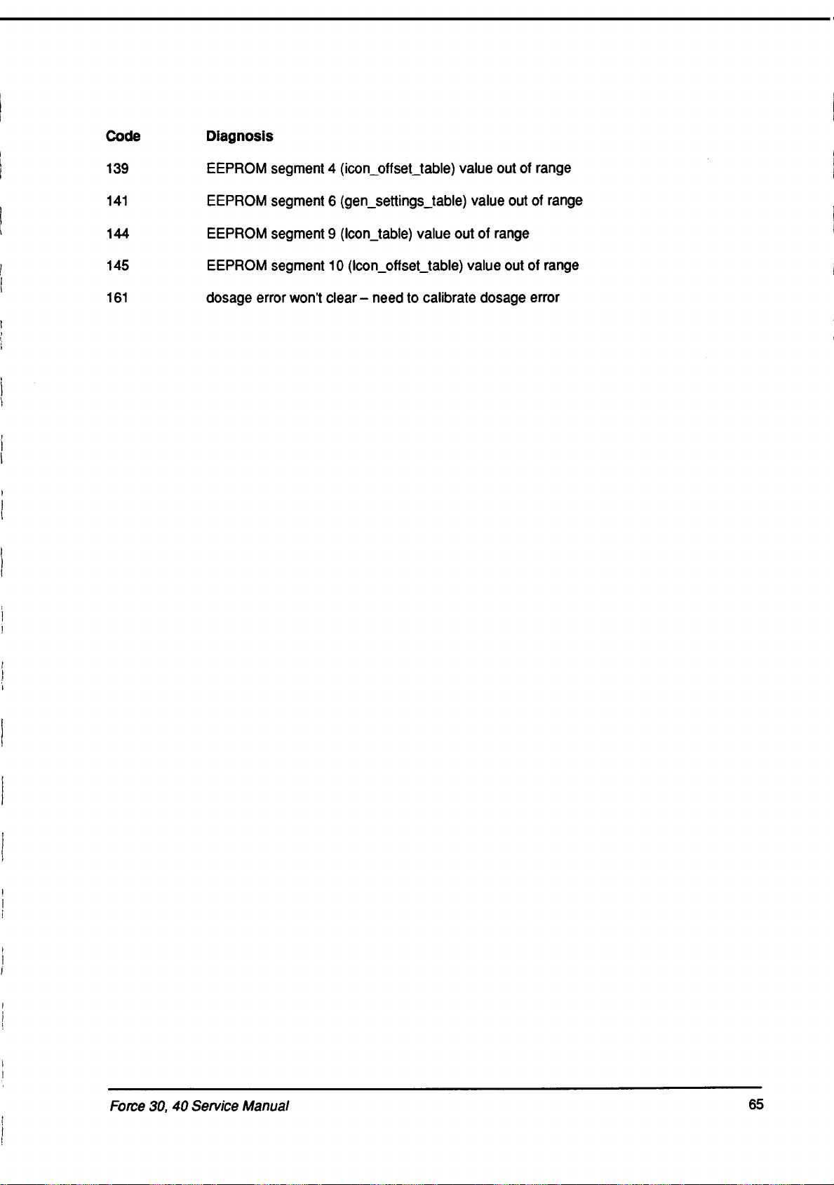
Code
139
141
144
145
161
Diagnosis
EEPROM
EEPROM
EEPROM
EEPROM
dosage
error
segment 4 (icon_offset_table)
segment 6 (gen_settings_table)
segment 9 (icon_tabie)
segment
won't
10
(Icon
clear — need
value
offset
to
value
value
out
table)
value
calibrate
out
out
of
range
out
dosage
of
range
of
of
error
range
range
Force
30,
40
Service
Manual
Page 74

66
Force
30,
40
Service
Manual
Page 75

Section 6 Component
WARNING
High
components
Ensure
generator
CAUTION
The
generator,
electrostatic
an
The
following
Install
1.
voltages
electrosurgical
antistatic
all
exist
on
on
the
PSRF
that
the
equipment
or
replacing
generator
work
at a static
sensitive
container
are
guidelines
nonpolarized
the
power
Printed
is
disconnected
components.
contains
control
components.
for
transport
that
relate
components
Replacement
connector,
Circuit
workstation.
Handle
of
electrostatic
to
so
power
Board.
from
the
electrostatic
Wear a grounding
the
circuit
sensitive
installing
that
the
and
value,
sensitive
switch,
the
AC
line
boards
mounting
tolerance,
aluminum
before
components.
by
components
disassembling
strap
their
nonconductive
components
and
heatsinks,
When
when
handling
and
circuit
on
part
number
and
the
repairing
edges.
boards.
the
circuit
are
certain
the
Use
boards.
visible.
Install
2.
polarization
.
Components
that
lead
leads.
.
Center
the
cathode
required,
.
Position
of
the
three
weight
.
Properly
with
another
.
Do
not
prevent
.
When
board,
.
installing
Mount
polarized
enters
the
with
lead-mounted
in
excess
insulate
stress
damage
insulate
resistors
components
markings
with
the
component
lead
longer
the
major
of
component
component
to
components
the
rated
are
coating
component
body
than
mounting
components
planes
1/2
ounce
all
component
the
component
sleeving
at 2 watts
so
visible
on
the
between
the
holes
(sides)
by
lead
or
leads
between
on
of
the
that
the
and
the
leads
body.
For
bends
anode
prior
so
of
the
means
leads
which
circuit.
and
circuit
components
or
less
positive
correct
may
have
example,
(except
lead
for
to
installation.
that
the
Unit.
Mechanically
other
than
are,
mounting
solder
boards
flush
pins.
with
to
symbol
polarity.
the
identification).
major
or
pins.
with
the
(+),
negative
coating
use a soldering
for
axis
the
could
the
metallic
circuit
removed
miniature
of
the
support
leads.
be,
forced
Provide
circuitry
bodies.
board
symbol
only
iron
to
diodes,
Line
component
an
on
(0.0 — 0.006
it
up
the
any
component
into a shorting
adequate
the
component
(—),
to
the
point
remove
is
desirable
leads,
is
parallel
strain
inch
or
other
where
coating
to
leave
where
to
any
having
condition
relief
to
side
of
the
clearance).
on
a
the
two
Mount
10.
circuit
Radial
11.
closer
surface
Force
30,
to
40
resistors
board.
lead
capacitors
the
body
to
the
potting
Service
of
greater
than
Manual
than 2 watts
(dip):
if
installation
0.06
inch.
material.
or
more
requires
Mounting
0.25 + 0.06
bending
height
should
inch
from
the
lead,
be
0.032 — 0.25
the
the
surface
bend
should
inch
from
of
the
be
the
printed
no
board
67
Page 76

12.
Soldered
13.
Control
14.
Remove
remove
surfaces
soldering
flux
residue
the
flux
residue.
should
temperature
on
be
the
clean
board
and
to
prevent
surface.
free
damage
of
contaminants
to
For
example,
that
components
use
isopropyl!
would
result
or
circuitry.
alcohol
in
poor
soldering.
and a brush
to
68
Force
30,
Service
40
Manual
Page 77

Section
Returning
Before
(1-800-255-8522)
assistance.
Attach a tag
Returning
you
e
HospitaVclinic
e
Technician's
e
Telephone
e
Department/address
e
City,
e
Model
e
Serial
e
Description
e
Type
7
the
return
Have
state,
number
number
of
repair
with
the
Factory Service
Generator
the
electrosurgical
for a Return
the
following
name/customer
name
number
and ZIP
of
this
Force
code
problem
to
be
done
same
30,
information
for
Service
generator
Authorization
information
number
to
40
Generator
to
Number,
ready:
the
generator
Valleylab,
or
call
when
call
the
your
shipping
Valleylab
Valleylab
it
for
Service
representative
service.
Department
for
Package
not
the
available,
e
Use a packing
e
Place a plastic
e
Use
non-abrasive
e
Use
four
Returning
When
packaging
e
Place
e
Provide a separate
Ordering
When
ordering
e
Model
e
Serial
e
Part
Number
generator
use
crossed
Circuit
each
in
the
following
container
bag
straps
Boards
circuit
PCBA
boards
or
the
over
packing
packing
Replacement
replacement
Number
Number
(located
(located
(refer
original
guidelines
with
double
the
generator.
material
to
secure
and
Other
or
other
subassembly
container
Parts
parts
for
on
the
rear
on
the
rear
to
Section
8,
packaging
the
container,
for
packaging:
wall
construction.
that
will
box.
Subassemblies
subassemblies,
in
an
ESD
for
each
the
generator,
of
the
unit)
of
the
unit)
“Service
Parts
if
available.
not
damage
use
(Electrostatic
PCBA
include
List”)
the
the
following
Discharge)
or
subassembly.
this
information:
If
the
surface
guidelines:
original
of
the
bag
packaging
generator.
or
container.
is
Force
30,
40
Service
Manual
69
Page 78

70
Force
30,
40
Service
Manual
Page 79

Section 8 Service
replaced
be
components
All
ratings
adversely
Note:
Valleylab.
Components
and
SAFETY
Display
REFERENCE
DESIGNATOR
Resistors
13,
8,
4,
R1,
12,
7,
5,
R2,
10,
9,
6,
R3,
24,25
R11,
R20
R35
R42
R43
R44
R51
R52
54
R53,
56
R55,
RA1-4
must
tolerances
affected
Patient
by
CRITICAL
are
marked
PCBA
19,
14,
18,
15,
17,
16,
must
be
substitution
COMPONENTS
23,
22,
21,
can
with
26,
27,
28,
29,
30,
31,
safety
equal
adversely
be
an
asterisk
32,
33,
34,
Parts
parts
with
or
better
of
lower
grade
must
affected
(*)
47,50
39,
36,
46,49
40,
37,
45,48
41,
38,
List
identical
of
than
original.
parts.
be
replaced
by
in
the
following
DESCRIPTION
56kQ+5%,
100
12kQ
4.3
43
51
1.2
750
82
10
1М
100
1k
1k
construction
Generator
only
alternate
of
use
listings:
5%,
+
Q
5%,
+
5%,
+
Q
k
1/2W
5%,
+
Q
+
Q
+
5%,
+
5%,
+
+
5%,
+
5%,
5%,
1/2W
5%,
5%,
1/2W
1/4W
1/4W
1/4W
015%,
k
Q
Q
+
Q
Q
Q
SIP
with
1/4W
1/4W
1/4W
1/4W
1/4W
1/4W
1/2W
value.
and
performance
parts
obtained
components.
Replacement
can
be
from
Safety
201
Critical
275
VALLEYLAB
NUMBER
PART
105
024
234
039
024
234
089
024
234
078
024
234
081
014
234
083
014
234
065
024
234
060
024
234
037
024
234
046
014
234
135
024
234
088
014
234
063
024
234
134
100
234
part
000
Capacitors
17,
16,
10,
C1,
14,
13,
3,
C2,
C4-9
22
21,
12,
C11,
29
26,
C15,
C33
integrated
U1*
3
U2,
U4
7,8
U5,
11
9,
U6,
U10
component
this
If
*
Force
30,
40
30,
23,
20,
24,
19,
18,
Circuits
replaced,
is
Service
Manual
31,
25,
32
27,
28
generator
the
must
20%,
+
uf
0.1
15%,
+
100pf
20%,
+
uf
1
+
uf
0.01
0.0033
0.001
pf
pf
+
X2402
LM7805
LM7812
PCF8574
SAA1064
DS3669
returned
be
50V
100V
50V
20%,
20%,
+
20%,
to
50V
100V
100V
Valleylab
for
007
118
204
013
200
204
014
118
204
001
118
204
031
200
204
025
200
204
008
720
210
083
300
210
085
300
210
016
760
210
800
210
800
210
recalibration.
full
015
017
Page 80

Transistors
Q1-
6
Q7
Q8,
9,
12,
Q10,
11, 14,
LEDs/Lamps
13,
17
15,
16
2N3904
VN10KM
IRFD110
IRFD9120
239
239
239
239
015
200
200
200
000
012
027
028
D1-8
11
10,
D9,
28
15,
53,
9,
16,
7,
70
14,
11
13,
56
16-18,
73,
50,
65,
46,
72,
43,
35,
34,
PCBA
66,
51,
D12-14,
D27,
Miscellaneous
OPT1
CR1-3
Interface
REFERENCE
DESIGNATOR
Resistors
R1,
R2
R3,
R4,
RS
R6,
R8,
R10,
R12,
R17,
R18
29,
28,
21,
R19,
R20
R23
110
R24,
86
R25,
R26
R27
38,
37,
36,
R31,
R33
77,87,97
R41,
112
74,
R42,
98
R47,
R48
20-26
93
76,
68,
75,
92
84,
30,
59,
79,
91,
85
32,
60,
80,
104,
39,
90,
89
111
44,
40,
103,
45,
107
94,
102
7-Segment
Lamp
LED
Bicolor
Reflective
Diode
Heatsink
DESCRIPTION
Q
k
75
910k
КО
33.2
Q
100
7.5k0
0+
13k
0+
k
27
100 k © + 1%,
k
100
6.49
Q
56k
Ω
330
015%,
1M
Q+
464
Q
332
КО
120
TRIMPOT
k
47
k
10
51.1
ΚΩ
220
TRIMPOT
1kQ+5%,
3.01
Ind.
RF
Lamp
Sensor
1N4148
5%,
+
5%,
Q+
+
5%,
+
1%,
+
1%,
5%,
5%,
2+
+
Q
k
+5%,
5%,
+
1%,
1%,
+
5%,
+
5
5%,
+
Q
5%,
+
Q
Q+
k
5%,
+
0+
k
Display
1%,
1%,
1/4W
1%,
10
1%,
12V
(red/green)
OPB703A
1/4W
1/4W
1/8W
1/4W
1/8W
1/8W
1/4W
1/8W
1/4W
1/8W
1/4W
1/4W
1/8W
1/8W
1/4W
k
1/4W
1/4W
1/8W
1/4W
k
1/4W
1/8W
239
750
051
077
200
215
063
750
239
052
750
239
053
750
239
000
014
239
223
400
546
276
201
VALLEYLAB
NUMBER
PART
108
024
234
134
024
234
435
201
234
039
024
234
373
201
234
396
201
234
097
024
234
234
201
481
111
024
234
367
201
234
105
024
234
051
024
234
135
024
234
257
201
234
243
201
234
113
024
234
006
010
236
103
024
234
087
024
234
453
201
234
119
024
234
007
010
236
063
024
234
335
201
234
002
72
Force
30,
Service
40
Manual
Page 81

234
201
201
201
201
201
201
024
201
201
024
201
201
201
024
024
024
024
318
457
531
365
393
350
055
402
519
118
357
330
510
046
077
110
082
075
R49,
R52
R54,
R55
R57
R58
R61
R62
R63
R81
R82
R83
R88
R95,
R96
R99
R100
R101
69,
64,
105,
71
67,
78
106, 108,
109
2.00 k Q+
56.2 k Q + 1%,
332 k O + 1%,
6.19 k 0+
12.1kQ+
4.32 k Q+
470
2+
15k
249 k Q + 1%,
200 k Q + 5%,
5.11k
2.67kQ+
200 k Q+
200 Q +
3.9 k 2 + 5%,
91 k O + 5%,
6.2 k Q + 5%,
3.3 k Q + 5%,
Q+
Q+
1%,
1%,
1%,
1%,
5%,
1%,
1%,
1%,
1%,
5%,
1/4W
1/8W
1/4W
1/4W
1/8W
1/8W
1/8W
1/8W
1/8W
1/8W
1/8W
1/4W
1/8W
1/8W
1/8W
1/4W
1/4W
1/4W
234
234
234
234
234
234
234
234
234
234
234
234
234
234 024
234
234
234
Capacitors
C1,
6,
24,
44,
C2,
5,
8,
10, 13, 16,
39,
42,
48,
48,
68,69,
C3,
C7,
C9,
C14,
C15,
C38,
106,
C41,
C45
C61,65
C88
C91,
C108-110,
C111,
C116,
11,
17,
51,
25,
23,
46,
107,
99,
92,
112
131,
72, 73,
12,
47,
52,
59, 71,
58,
70
32
40,
56,
82,
83,
117-124,
100,
96,
97
113-115,
132
62,
67
18,
49,
50,
74,
76-81,
54,
64
84
75
85,
89,
127,
103-105,
125,
19,
53,
55, 57,
86,
90, 93,
128
133
126,
21,
22,
87, 95,
94, 98,
129,
26-31,
60, 63, 66,
101,
130
33-87,
102
0.01uf + 10%,
0.01
pf + 20%,
1000pf + 10%,
1000pf + 15%,
22
pf + 15%,
10
pf + 10%, 25V
1500
pf + 10%,
0.1
uf + 20%,
1
uf + 20%,
0.47
pf + 20%,
330pf + 5%,
220
pf + 20%,
100pf + 5%,
10
pf + 20%, 6 kV
0.0022
0.0047
uf + 10%, 6 kV
pf + 20%, 6 kV
50V
50V
50V
100V
100V
50V
50V
50V
50V
35V
100V
NPO
NPO
50V
NPO
NPO
204
200
284
204
118
001
204
200
273
204
200
025
204
200
005
204
102
008
204
200
275
204
118
007
204
118
014
204
118
012
204
200
268
204
500
124
204 200 013
204
200
286
204
025
044
025
204
050
Force
30,
40
Service
Manual
73
Page 82

Integrated
U1,
7,
18,
24
U2,
14, 17,
U3,
5,
U6
U8,
15,
U9
U10
U12,
U13
U23
U25
U26
U27
U28,
U29
U30
U31
U32
Diodes
CR1,
CR2,
CR11
CR25-29
11, 16,
21
22
33
7,
12,
3, 6,
19
13,
8-10,
Circuits
20
20-24
14-19
LF412
XR-2228
LM331
74HC14
DG445
LM339
LM336
LM393
LM2917
74HC00
LM386
TDAB444
LM7805C
LM7812C
PCF8574
LM7912C
74HC74
DS3669
1N4148
1N5236B
1N5817
VSB52
210
400
210
100
210
740
210
230
210
200
210
300
210
300
210
300
210
750
210
300
210
400
210 750
210
300
210
300 085
210
760
210
300
210
230
210
800
239
014
239
600
239
700 005
239
700 025
016
030
007
004
041
015
016
011
003
007
019
004
083
016
087
006
017
000
636
Relays
K1-4
Miscellaneous
013
Q4
T1,8
T2-7
HV
Reed
Relay
FET
VN10KM
FET
IRFD110
Inductor,
Transformer,
Current
Heatsink
Sense
isoBloc
230 009
239 200
239
200
251
300
251
300
223
400
000
012
027
008
006
546
74
Force
30,
40
Service
Manual
Page 83

Microprocessor
REFERENCE
DESIGNATOR
Resistors
R1,
3,
6-9,
14-22,
R2
R4,
23
R5
R10
R11
R12
R13,
29-32
R33
RA1,
RA3
RA2
Capacitors
C1,
2,
5-7,
9,
41-52,
C3,
53,
C20,
C32-34,
C80,
54-58,
4,
8,
10-12,
59-64,
25,
71,
87
39,
82
13,
14,
65-70,
15,
78,
40
24-28,
16, 18,
83,
PCBA
34-39
17,
21-23,
72-77,
19,
85,
86,
26,
28,
79, 81,
24,
27,
88
35-38,
84
29-31,
DESCRIPTION
330 Q +
100
10k
k
Q+
Q
5%,
5%,
+
5%,
1/4W
1/4W
1.8 k Q + 5%,
1kQ+5%,
10k
0+
6.81 k Q+
2.2k Q +
270
2+
Resistor
Resistor
0.01
uf + 20%,
0.1
uf + 20%,
1
uf + 20%,
330
pf + 5%,
22
pf + 5%,
1/4W
1%,
1%,
5%,
5%,
1/4W
Array
Array
50V
100V
100V
1/8W
1/4W
1/4W
1/8W
1/4W
3.3
k
1
50V
50V
k
201
278
VALLEYLAB
PART
NUMBER
234
024
051
111
024
234
234
024
087
234 024
234
234
234
234
234
234
234
204
204
204
204
204
024
201
201
024
024
100
100
118
118
118
200
200
069
063
385
369
071
049
097
168
001
007
014
019
005
003
Integrated
U1
υο
U3
U4
U5
U6
U7,
12
U8
U9
U10
U11,
14,
15
U13
U16
U17,
19
U18
U20,
23
U21
U22
U24
U25
Circuits
DS8921
74HC393
74HC02
74HC240
LM393
LM336
DG445
LM339
LF444
79L12
74HC14
LM78L12
DAC1230
DAC1006
74HC138
74HC373
DS1232
80C196
27512
6264
EPROM
SRAM
210
800 013
210
220
210
230
210
230
210
300
210
300
210 200
210
300
210
400
210
300 092
210
230
210
300
210
750
210
750 000
210 230
210
230
210
760 015
210
710
210 730
210
770
393
011
009
011
016
041
015
017
004
091
005
003
001
004
092
001
Force
30,
40
Service
Manual
75
Page 84

U26
U27
Transistors
Q1,
Q2
Diodes
CR1-3
Crystals
x1
Transformers
T1,
2,
3
Miscellaneous
Power
Supply
PCBA
PAL14L4
LM7805CT
VN10KM
1N4148
11
MHz
Dual
Pulse
Heatsink
Transformer
210
790
210
300
239
200
239
014
250 010
251
300
223 400
201
277
005
083
012
000
015
010
546
000
REFERENCE
DESIGNATOR
Resistors
R1,2
4
R3,
R5,
7,
10,
12
R6,
8,
11, 13,
87,
89,
RQ
84
R14,
R15
R16
R17,
20 27
R18,
19
R21 150 © +
R22,
40
R23
R24,
31-34,
R25
R26,
64,
R27
R28
R29,
79
R30
R35
91,
71,
37,
93,
95,
39,
73-75
42,
96
46,
44,
66,
49,
78
54,
77,
81,
82,
DESCRIPTION
20kQ+5%,8W
Thermistor
51 Q +
1kQ+5%,
150
2+
2+
100
6.98 k Q + 1%,
1.8k Q +
Q+
4.7 Q +
200 k Q + 5%,
1.6k O +
10 k Q + 5%,
2.7 k Q + 5%,
100 k Q + 5%,
330 O +
68 k Q + 5%,
10
2+
787 O +
39 k O + 5%,
5%,
5%,
5%,
5%,
5%,
5%,
5%,
5%,
5%,
5%,
1%,
1/4W
1/4W
20W
1/4W
1/8W
1/4W
1/4W
1/2W
8W
1/4W
1/4W
1/4W
1/4W
1/4W
1/4W
1/4W
1/4W
1/8W
1/4W
VALLEYLAB
PART
NUMBER
017
000
234
003
003
240
234
024
032
234 024
234
234
234
234 024
234
234
234
234
234
234
234 024
234
234
234
234
234
234
400
024
201
024
014
400
024
024
024
024
024
024
024
201
024
063
251
039
370
069
025
060
250
118
068
087
073
111
051
107
015
279
101
76
Force
30,
40
Service
Manual
Page 85

234
024
R36,
R38,
R43
R45
R47
R48,
R51
R52
R53,
R55,
R56,
R57
R58
R59
R61
R62
R63
R67
R69,
R76
R85
R86,
R97,
41
50,
83
60
68
72
65
70
88, 90, 92,
98
94
2kQ+
10M Q +
91k
430 O +
75
20 k O + 5%,
390
9.09 Q +
470 Q +
5.1k
Trimpot
430 k O + 5%,
51 k Q + 5%,
30 k O + 5%,
47
270 k O + 5%,
18k O +
4.7kQ+5%,
510 O +
2.2k0+5%,
27
4.7 0 +
150
5%,
5%,
025%,
5%,
КО + 5%,
2+
5%,
1%,
5%,
015%,
20
k
КО + 5%,
5%,
5%,
КО + 5%,
5%,
Q,50W
1/4W
1/4W
1/4W
1/4W
1/4W
1/4W
1/4W
1/4W
1/8W
1/4W
1/4W
2W
1/4W
1/4W
1/4W
1/4W
1/4W
1/4W
1/2W
1/4W
1/2W
234
234
234
234
234
234
234
234
234
236
234
234
234
234
234
234
234
234
234
234
234
234
070
024
158
024
110
024 054
024
108
024
094
024 053
201
381
024
055
024
080
200
080
024
126
024
104
024
098
024
103
024
121
024
093
024
079
014
096
024
071
014
006
024
007
003 005
Capacitors
C1,2
C3
C4
C5
C6,
7,
32, 34,
C8,
10,
12, 16,
C9,
35,
37,
72,
73,
C11
C17
C28
C30
C48
C50,
C51,
C52,
C54,
C56
C66,
C68,
C70,
13-15,
39,
76-79,
59
53,
58,
75
61
67
69
71
18-21,
41-47,
36,
22,
82, 85,
62
38,
25,
23,
49,
40,
83,
81,
84,
24,
26, 27, 29,
55, 57,
88,
91,
102
87,
60,
98,
90,
63,
101
97
31, 33,
64,
65,
1000
pf
+50% — 10%,
2
uf + 10%,
0.0015
1
1
0.01
0.1
0.47
180
1500
680
330
1000
0.047
220
0.33
750
15
4700
470
pf + 5%,
uf + 10%,
uf + 20%,
uf + 20%,
uf + 20%,
if + 20%,
pf + 20%,
pf + 10%,
pf + 5%,
pf + 15%,
pf + 15%,
pt + 20%,
pf + 10%,
pf + 20%,
pf + 10%,
uf + 10%,
uf
+30% — 20%,
if
+30% — 20%,
400V
500V
250V
50V
50V
50V
50V
100V
50V
500V
100V
100V
50V
50V
50V
500V
200V
400V
NPO
NPO
35V
35V
204
500
204 400
204
105
204 400
204
118
204
118
204
118
204
118
204
200
204
200
204
105
204 200
204
200
204
118
204
200
204
118
204
106
204
400
204
500
204
500
159
001
030
153
014
001
007
012
016
275
022
019
025
005
266
011
031
150
158
125
Force
30,
40
Service
Manual
Page 86

204
102
085
080
200
030
007
000
013
C86,
89,
C93
C94,
95
C103
92,
99,
100
22
uf + 20%,
9100
pf + 5%,
7500
pf + 5%,
100
pf + 5%,
35V
500V
500V
100V
204
204
204
Integrated
U1
U2
U3,
6
U4
US
U7
U8
U9
U10
U11,
14,
23,
29
U12
U13
U15,
16,
17,
22
U18
U19
U20
U21
U24-28
Diodes
CR1-4
CR5-15,
CR16,
CR18-20
CR21
CR22-25
CR26
CR32-35
CR37
CR80
27,
17
Circuits
28, 30,
31,
36
UC3825
8
MHz
74F393
82S185A
74HC74
16L8
PAL
74HC123
16L8
PAL
LM7912C
LM7812
LM7805
LM7905
LT1016
TLO52
DG445
MC34082
LM319
TSC4429
FES8JT
1N4148
1N5228
Full
Wave
1N5239
1N5235
LED
MUR880
1N5231B
MDA3504
X-TAL
PROM
Programmed
Programmed
Bridge
Programmed
200V
300
210
250
010
210
220
210
730
210
230
210 790
210 230
210 790
210
300
210
300
210
300
210 300
210
410 000
210
400 020
210
200
210
400
210
410
210
800
239
700
239 014
239
075
239
700
239 600
239 600
239
750
239 700
239
600
239
700
081
017
394
088
006
006
012
007
087
085
083
093
041
021
001
014
051
000
000
050
638
637
011
055
003
003
Transistors
Q1-4
Q5,
10, 12,
Q6,8
Q7,9
Q11
Q14-17
Q18
Transformers
T
T2
T3,5
T6
78
13
IRFBC40
VN10KM
IRFD110
IRFD9120
2N3906
APT8075
BUZ80
Switching
Pulse
Transformer
RF
Transformer
Transformer
Output
Transformer
PE-52686
Force
239
239 200
239
239 200
239
239
239
251
251
251
251
30,
40
200
026
012
200
027
028
047
000
200
033
200
020
200
047
300
014
300
008
200
052
Service
Manual
Page 87

Miscellaneous
215
100
F1
K1
上
1
L2
2
16
17
25
39
Fuse,
F6.3
Relay
AZ421
Inductor,
Cut
Heatsink
Heatsink
Heatsink
Heatsink
Heatsink
0.75mH
Inductor,
Amp
4.1
WH
230
251
251
223
223
223
223
223
041
007
002
039
000
100
077
400
521
400
508
400
529
400 546
400
543
Force
30,
40
Service
Manual
79
Page 88

201
299
REM
Filter
PCBA
000
REFERENCE
DESIGNATOR
Resistors
R1-4
R5,
12
R6,
9-11
R7
R8
R13
R14
R15,
22
R17,
18
R19,
24
R21
Capacitors
C1-5,
14, 15,
C6,
12,
13
C7,8,9
C10,
11
C16,
17
C18
19-21
DESCRIPTION
100 k © + 5%,
15k O +
5.6 Q +
1kQ+5%,
Trimpot 2 k
10k O +
Trimpot
8.2 k Q + 5%,
2 k Q + 5%,
4.7 k Q + 5%,
12 k Q + 5%,
0.01
1.0
0.1
10
0.22
330
5%,
5%,
1/4W
Q
5%,
20 k 92
1/4W
mf + 20%,
pf + 20%,
uf + 20%,
pf + 10%,
uf + 10%,
pf + 5%,
1/4W
1/4W
1/4W
1/4W
1/4W
1/4W
1/4W
50V
50V
50V
25V
250V
500V
VALLEYLAB
PART
NUMBER
234 024
234
234
234
236
234
236
234 024
234
234
234
204
204
204
204
204
204
111
024
091
024
081
024
063
010
105
024 087
010
108
085
024
070
024
079
024
089
118
001
118
014
118
007
102
008
400
120
105
014
Integrated
U1,5
U2
U3
U4
U6
Transformers
τι
Circuits
IC
Quad
Analog
LF412
74HC14
4013B
LM393N
Transformer — RF
Switch
Input
210
200
210
400 016
210
230
210 027
210
300
202 900
041
004
001
011
017
80
Force
30,
40
Service
Manual
Page 89

Section
Electronic
Cable # 1:
Pin
Assignments
Low
1
3
4
5
6
7
8
9
10
11
12
9
Assemblies
Interface
Voltage
Frame
digital
HC-DATA
digital
IIC-CLK
digital
IIC-INTO
digital
+9
unregulated
+15
IIC-INT1
digital
Interconnect
Ground
ground
ground
ground
ground
unregulated
ground
Between
Cable
and
Boards
Schematics
25
26
27
28
29
30
31
32
33
34
35
36
digital
ground
FREQO
digital
ground
FREQ1
digital
ground
FREQ2
digital
ground
FREQ3
digital
ground
BIPHSW
digital
ground
ACC-CUT
13
14
15
16
17
18
19
20
21
22
23
24
1IC-INT2
digital
ground
+5
IIC
digital
ground
digital
ground
AUDIO-FREQ
digital
ground
VPOT
digital
ground
DOS-FREQ
digital
ground
DOSERR\
37
38
39
40
41
42
43
44
45
46
47
48
49
50
digital
ground
ACC-COAG
digital
ground
ISOCLK
digital
ground
HSWO
digital
ground
HSW1
digital
ground
HSW2
analog
—15
analog
+15
ground
unregulated
ground
unregulated
Force
30,
Service
40
Manual
81
Page 90

Connector
Signals
voltage
A15
analog
Al
B1
C1
A2
B2
C2
A3
B3
C3
A4
B4
C4
A5
B5
C5
#1:
Microcontroller
through
IIC-DATA
IIC-CLK
IIC-INTO
UC-INT1
IIC-INT2
AUDIO-FREQ
digital
digital
C16
and
digital
ground
DOS-ERR\
DOS-FREQ
ground
FREQO
FREQ1
ground
digital
FREO2
FREQ3
for
are
lines.
Board
isolated
the
to
PSRF
Board
footswitch
circuits.
A9
The
B9
C9
A10
B10
C10
A11
B11
C11
A12
B12
C12
A13
B13
C13
remaining
digital
MODE0
MODE1
digital
MODE2
CUTREL
RF-RESET
RF-LMT
ECON
ICON
LCON
AUTOPOT
unregulated
=-15
=
unregulated
+15
unregulated
+9
signals
ground
ground
are
low
A6
B6
C6
A7
B7
C7
A8
B8
C8
ground
digital
BIPHSW
ACC-CUT
ACC-COAG
ISOCLK
HSWO
ground
digital
HSW1
HSW2
A14
B14
C14
A15
B15
615
A16
B16
C16
reserved
reserved
reserved
RFJBIP
RFJCOG
RFJCUT
FFJCOG
FFJCUT
FJCOM
isolation
for
isolation
for
isolation
for
82
Force
30,
40
Service
Manual
Page 91

Front
Panel
Restore
eyboar
Bipolar
Keyboard
Monopolar
Keyboard
REM
Front
Footswitch
ps...
,
External
à.
Jeminal
PCBA
J502
P502
____
|
J5o1lPso1
4
|
|
|
|
|
|
|
I
|
|
|
|
|
|
.
:
©
i
|
Handswitch
|
Receptacie
|
|
|
Accessory
|
Receptacie
너그
P408
Internal
Cover
Assembly
A
P902
4202 9208
|J208
J212 4206
J601|
Paoe
Front
Panel,
|Р903 _ _Р904|
Interface
REM
Fitter
dicono
4204
PCBA
1201
P301
P804 | 1304
Footswitch
Receptacle
Bipolar
Receptacle
P905
9205
J207 | P207
4209[Р1009_
T306
High | Peo1ir コ J301
voltage
—
LI
———aromrane
| |
3103]
P103
Display
PCBA
3
| |
|
|
|
|
|
#
A
P303 P908
J303
PSRF
4104
4105}
J106
P1006
PCBA
J312r—1
[トー
Р104
Р105
P712
|
| |
I
1
|
|
|
|
|
|
|
1
|
|
L 一 一 一 一 一 一 一 一 一 一 一 一 一 J
Microprocessor
J308
ree
Assembly
Heatsink
J307 | P307
able
J306 | P806
—_——=
eee
eee
ee
ewe
ee
ee
fe
ee
ee
ee
ee
Line
Cord
—
m
Force
30,
40
Service
сои
reaker
Manual
O
ee
O
me
Figure
J302 J314
P802
~
6815 | 4315
9.1
System
Transformer
Rear
PB14 P805
=
mos
Voltage
Panel
Interconnect
mo
amoo
cmi
ct
ce
emp
Volume
Control
Diagram
J305
to
ft
co
tos
ent
co
to
fato
to,
o,
o,
mo mo
e, e,
Rear
Bipolar
Footswitch
Rear
Monopolar
Footswitch
83
cm
maos
mr
me
Page 92

|
n
W5A $ изв
|
J1
RE
49
Mono
Ὕ
ont
“了
C116
==
61ΠΕΙ1
26
95BJSiul
3ieuusu5S
po
92104
‘08
Op
S01A18S
[OSS-FREO)-
[епиви
+
Waa
ei
一
C132
k
C109
C110
-一
0115
σι
HH
C130
ph
A
I
C108
上-
|
0114
0113
T2
4
AZ
RFBIP-
ος
C129
T8
was
ns
$
1
T
C11
С12
一
1
AFBIPs
cet
2
TURNS
『
^
=
=
|
1
그
T
Rot
$
«
!
$
ar
>
pan
$
4
$
>
nes
Res
ce
VMONO-
CRE
CR8
1
CR10
CR9
REM-AC
VBIP+
cris
CR14
var-
CR17
CR16
BP
CR19
CR18
2
|
{
|
18
E
0218
15
8
Т
Uz1C
10 a À
C43
44
[Dr
CM
C
[
4
]
ar
사브
16
ja
11
[
4
VOX
KLD,
V-CLK
нак
Cauro]
7
4
As
Γ
」
+5!
cag
VMONO+
IMONO
VMONO-
УВ»
VBIP-
971
$
$
$
rss
$
Hone
V
」
urs
€
Vw
11
42
$
|
上
cso-
マ
3
+
と
“E
——
V-
USA
m
Reo
$
857
121K
-12
-
>
è
12
R62
8
056
бо
4
Р-
+12
」
14
|
zel
^
c
』
$
Ἱ,
|
Sao
165
E
Ui68
R27
3
C52
«12
Page 93

6910
06
OP
9οιλιθς
jenuey
76
panuiuos
g8
PWR-MONO
>
>
«
они? Ž R63
1
"T
"
AAA
AN
o
R2
BiP
+12
Sa
35
^
p
PWR-BIP
R42
8
ANA
C24
4
U7B
R434
27
+12
4
。
10
C40
RSI
D
del
TP12
O
1
y
Ê
1
+5
A
VREM
νν
vasip__
R112
we
d—
8
om
+12
any.
-12
pop
T
|.
|
“2
RY
~
3
R20
79
νν
R77
2
MA
, a
ツン
JS
R87
AAA
ΤΡΙ
0
TP4
©
MUXO
6
5
=
C67
2
2
νι8
8
U18B
R92$
$
i
|
+
|
)
a
2
「
CR13
fer
CR20
4
fer
cr
11416.
LM331
Vec
EF
y
R
GNU
く
Re5
j
1
マ
和
>
я
V
VC
К
GNÚ
gr
L
L
+
İ
$
~
て
+
V R
GN
+
R16
AAT
023
2
Bo
AE.
8
2
nas
C75
NAV
8111
ON
TP2
0
TPS
res
0
5
EBEO0A
rat
A,
FnEos
|
——
ure
FREOO..3]
K
FREGIO..3]
d
|
Page 94

¡ENUEN
——.
C79
99195
ϱΡ
“DE
ce
U10
è
3
R49
αλλ...
vw
©
a
©
ISOREF1
+
y
I
L..
+12RELAY
L
TP3
92/0
+12
fm
panunuos
50
PO
+
15UR
AUDIO-FREQ
GND
ド
C
GE
引
一
一
1
088
49
4
ро
P——©
AGND
AGND
omy
U25
Gi
УЗ
I
36
43
45
41
5
D—-0
Den
LS
90
0
OGND
HSW2_
„VOLUME
VOLUME-POT
ce?
GNO
GND
GND
воск
HSWI
HSWO
AUDIO-THROTTLE
R97
+
2
37
GND
ACC-COAG
30
3
35
=
>
0
ano
BIP-HSW
E
р
一
AUDIO-MIN
R99
i
"DI
È
cos
coo
1
οι
bi
==
ci
23
22
р
P
[Εβεπία
α
>
A
CR23
κ
CR24
a:
19
O
GND
VOLUME-POT
|
rem
1P18
25
23
Sb
P
È
-15UR
©
изо
м
8
VOP—2—4-0
-12
+1SURRFO-F—
U33
VI
в
vaio
+12RELAY
14
12
18
17
GND
GND
GND__AUDI0-FREQ
GND
muro
J
주
093
VW
ç
8
2
voka—-e*l?
0%
=
13
eur
+
L
C89
zo
$
G“
στα
+5
98
19
8
9
8
7
GND
GND
+9UR
+1SURRF
cod
+
cx
+
„ыко
+
GND
=
U28
4
CR22
U27
κ
CR21
S
4
1
сю
Как
в
F
ane
Rios
2
a
2
,
2
g
+
g
pi
1
the
a
GET
BASS
BEE
BACI
AGI
SEE
=
lo
τα
AUDIOTHROTTLE
O
TP16
TP15
T
+
Page 95

109-95
691
μια!
Sty
87
1180
ιο
ocean
OMSH
>
ved
dem
86n
cen
pore
Fr
4540S!
60
PM
?
|
ゴト
een
+
v
før
ic
o
9
z+
a
rey
ει
£
rà
νι
İanoosı>
92080
9080
suo
F
E
0010
p
mio]
of
f
бы
=]
BEM
61H
MIOS!
6110081
continued
9.2
96ο
949
veen
IST
VO9-OOY
MSH-dig
Otdi
vn
oen
43HOSI
Tx
VEM
nr
вен
r
|
vy
asn
<]
91
Os!
sr
VOM
vr
BIM
Manual
Service
40
30,
Force
Page 96

88
-1
ain5d
56
JSAod
HIddnS
25meusuoS
99104
'0E
Op
SINOS
JENUBW
WAK-FREO
PAL
RENANE
FOR
=
no_caco
CI
AE
Dos-EBEQ__GN8
<
BEDO
Ω
Q2
03
BIPHSW
ACC
АСС-СОАС
o
HSWO
HSM
HSM
GND
0
h
RE
RİK
PIN 1 FGND
SEPERATION
GNS
GNB
std
+15URR ウ ーー
GNS
NES
CNS
GNS
GNS
GNS
GN8
GNG
GNB
GNB
_GNE
GNB
ΟΝΕ
GNO——4
GNE
WS
Bumper
Е
=
с
а
с
y
о
=
с
8
о
o
o
a
a
RENAME
AGND
FOR
PIN
GND
47848
SEPERATION
Usa
REXT-CEXT
CEXT
q
+12A
-12А
С72
C73
ISENSE
TP15
TP11
E
Page 97

JP2
95104
‘0$
ΟΡ
SIMAS
ΙΡΠΙΒΙΝ
£'6
penunuoo
R814
4
>
By
x = Y
JP1
R88
68
VSENSE
1218
—12A
VPEAK
‹
sz
>
も
8
€
>
Page 98

06
CRI
5'6
репициоэ
©
cas
7021
C4
O
C40
TP10
TP13
TP18
TP9
TP
12
©
+15UR
Τ
Tess
-15UR
$
2
as
Του
~15UR
Es
«pe
R3
+
ì
RON.
一
四
站
E
和
TT
+
İRİ
o
©
=
9
0
+15URRF
+15URR
14 y go
GAR
+15URRF
—
Toe
+15URRF
=
Tes
+9UR
“τν
037
LAV
1
U29
U23
м
U14
U12
м
CR36
2
CR31
8
2
“=
CR10
gr
2
—
>
CR12
8
2
~
+12C
©
3
T
+128
ør
C102
C8
vor
+12
3
a
cx
+5
νο[--3
ca
U11
γι
U10
м
U13
CR14
g
2
CAN
8
1
V
CR13
+12A
T
-12A
3
die
T
SA
ørn
99/04
‘0E
Op
99IM9S
JENUEN
J8
sara
FFJCOG
J5
NA"
&
=
ON
NARA
O
J4
Page 99

92104
‘08
др
ээмлас
jenuey
g6
penunuoo
+6
JUMPER
T3
Page 100

2
90356
95935
V-D35
a
2“
“AM,
000-060
LUIS
TEST
ET
Ed
td
=
점
ONO
oo
2
on
“4
っ
G+
Lope?
au
ONS+
39-935
3-035
oe
5
T
SCdSO
УСТ
TEST
ZOSST
eg
le
dd
vos
ws
vr
te
=
그
Vw
9118
OST
Oy
oNy
NV
sejodia
И
上
で
0379+
Nr
Nasi
ea
аи]
a
|
Sid
"9
eld
Sid
A
e
o
ειο
=
nu
10
Nostra
TI
gid
ΖΧ
хи
o
é
oust
og
inv
60
Le
5
+
910
“İŞ
4
atu
“et
y
VIVO-ONI
Ш
SL
9935
5
ISIN
TOSUN
ТРО
N
_
#19
614
$335
POLE
mur
"ola-dsa
"ola-d
0
VIVE
CE
УР
MM
#-936
w-Das
sa
Lojy-dsQ
UgerSSU
td
994
Ln
beer
Sar
1
0-938
2-938
7938
;
Ὃ
ZY=TASU
т
Petas
τοσα
9d
га
νά
Ed
OND
=
=
060
es
°
h
Sarasa
mů
t
ed
SE
#2
Mi
I
958
+
ory
NIN
-
i-
ow
+
мо
E
0379+
和
Nera
Nー
一
て
errasn
Erasg
esa
一
RI]
一
사기
上
cid
Sid
bid
Hav
T
=
iv
vo
Ne
Netos
Sid
219
ον
=
TI
хи
хи
o
so
T
于
oe
ONV
им
40
m
=
|
AN
DA
ΝΙΝΟ-ΟΙΙ
Ш
Joss
DOS
ds
9-935
8935
7938
+936
上
2
rm
PETISTA
Zİ
παν
Tartas
TESTIST
TS
o”
N
—
NN
29
=
=
osu
у
Οἱ
Ню
936
6809
ola-dsa
EP
TESTA
92
a
y
ar
Figure
ano
ーー
og:
<
È
9.4
——_——————Ò
O1NI-OIl
YN6+
ONO
QNo
O0]
Ol]
od9
qs
9
6
Display
Board
2LNI-Oll
ΗΝΙΓΟΙΙ
Hnzl+
AND
nes
Querem]
0-4
21
OL
||
DIST
ans
OND
o—d
o—d
ひ
ーーd
エー
9!
vi
Si
Schematic
Force
30,
40
Service
Manual
 Loading...