

UNITRODE UCC1808-1, UCC1808-2, UCC2808-1, UCC2808-2, UCC3808-1 Technical data
...
查询UCC1808-供应商
Low Power Current Mode Push-Pull PWM
UCC1808-1/-2
UCC2808-1/-2
UCC3808-1/-2
FEATURES
• 130µA Typical Starting Current
• 1mA Typical Run Current
• Operation to 1MHz
• Internal Soft Start
• On Chip Error Amplifier With 2MHz
Gain Bandwidth Product
• On Chip VDD Clamping
• Dual Output Drive Stages In Push-Pull
Configuration
• Output Drive Stages Capable Of
500mA Peak Source Current, 1A
Peak Sink Current
DESCRIPTION
The UCC3808 is a family of BiCMOS push-pull, high-speed, low power,
pulse width modulators. The UCC3808 contains all of the control and drive
circuitry required for off-line or DC-to-DC fixed frequency current-mode
switching power supplies with minimal external parts count.
The UCC3808 dual output drive stages are arranged in a push-pull configuration. Both outputs switch at half the oscillator frequency using a toggle
flip-flop. The dead time between the two outputs is typically 60ns to 200ns
depending on the values of the timing capacitor and resistors, thus limits
each output stage duty cycle to less than 50%.
The UCC3808 family offers a variety of package options temperature range
options, and choice of undervoltage lockout levels. The family has UVLO
thresholds and hysteresis options for off-line and battery powered systems.
Thresholds are shown in the table below.
Part Number Turn on Threshold Turn off Threshold
UCCx808-1 12.5V 8.3V
UCCx808-2 4.3V 4.1V
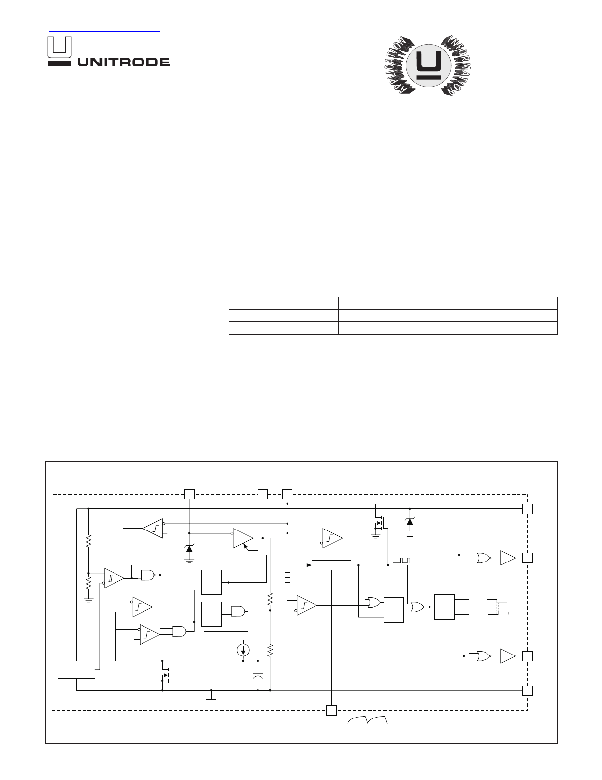
BLOCK DIAGRAM
OVERCURRENT
COMPARATOR
VDD OK
VDD–1V
0.5V
VOLTAGE
REFERENCE
0.75V
SOFT START
FB COMP CS
2.0V
2.2V
S
Q
R
S
Q
R
SLOPE = 1V/ms
VDD
1.2R
R
312
PEAK CURRENT
COMPARATOR
0.5V
OSCILLATOR
0.8V
PWM
COMPARATOR
VDD
8
14V
7
OUTA
PWM
LATCH
S
Q
R
4
RC
Q
T
Q
6
OUTB
5
GND
UDG-99076
04/99
ABSOLUTE MAXIMUM RATINGS
Supply Voltage (IDD ≤ 10mA) . . . . . . . . . . . . . . . . . . . . . . . 15V
Supply Current . . . . . . . . . . . . . . . . . . . . . . . . . . . . . . . . . 20mA
OUTA/OUTB Source Current (peak) . . . . . . . . . . . . . . . . –0.5A
OUTA/OUTB Sink Current (peak) . . . . . . . . . . . . . . . . . . . 1.0A
Analog Inputs (FB, CS) . –0.3V to VDD+0.3V, not to exceed 6V
Power Dissipation at TA = 25°C (N Package). . . . . . . . . . . . 1W
Power Dissipation at TA = 25°C (D Package) . . . . . . . . 650mW
Storage Temperature . . . . . . . . . . . . . . . . . . . –65°C to +150°C
Junction Temperature. . . . . . . . . . . . . . . . . . . –55°C to +150°C
Lead Temperature (Soldering, 10sec.) . . . . . . . . . . . . . +300°C
Currents are positive into, negative out of the specified terminal.
Consult Packaging Section of Databook for thermal limitations
and considerations of package.
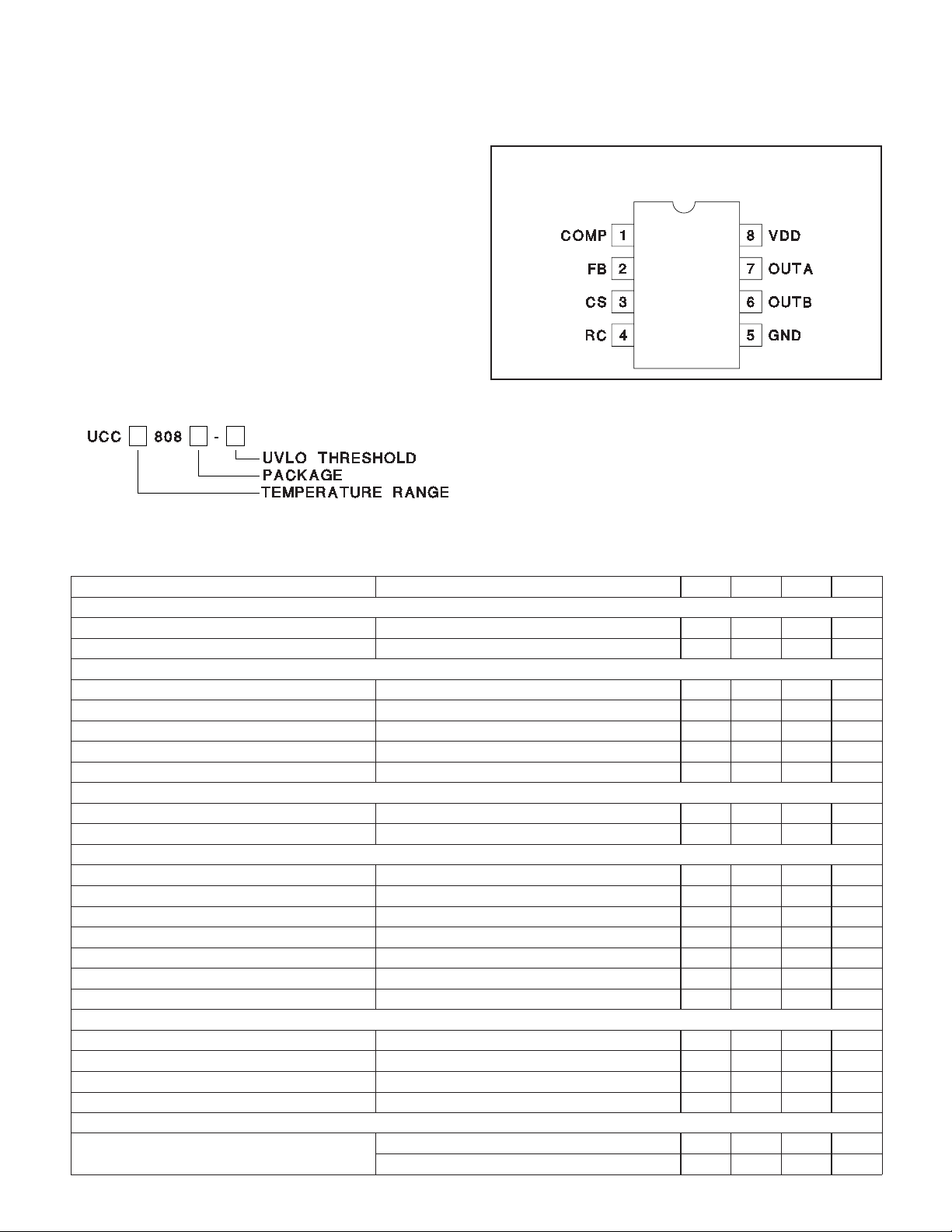
ORDER INFORMATION
UCC1808-1/-2
UCC2808-1/-2
UCC3808-1/-2
CONNECTION DIAGRAM
DIL-8, SOIC-8 (Top View)
J or N Package, D Package
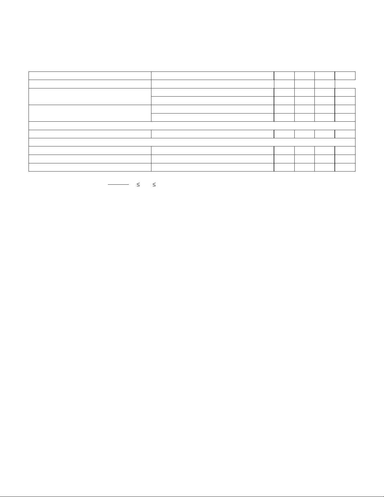
ELECTRICAL CHARACTERISTICS:
the UCC2808-X and –55°C to 125°C for the UCC1808-X, VDD = 10V (Note 6), 1µF capacitor from VDD to GND, R = 22kΩ,
C = 330pF. TA=TJ.
PARAMETER TEST CONDITIONS MIN TYP MAX UNITS
Oscillator Section
Oscillator Frequency 175 194 213 kHz
Oscillator Amplitude/VDD (Note 1) 0.44 0.5 0.56 V/V
Error Amplifier Section
Input Voltage COMP = 2V 1.95 2 2.05 V
Input Bias Current –1 1 µA
Open Loop Voltage Gain 60 80 dB
COMP Sink Current FB = 2.2V, COMP = 1V 0.3 2.5 mA
COMP Source Current FB = 1.3V, COMP = 3.5V –0.2 –0.5 mA
PWM Section
Maximum Duty Cycle Measured at OUTA or OUTB 48 49 50 %
Minimum Duty Cycle COMP = 0V 0 %
Current Sense Section
Gain (Note 2) 1.9 2.2 2.5 V/V
Maximum Input Signal COMP = 5V (Note 3) 0.45 0.5 0.55 V
CS to Output Delay COMP = 3.5V, CS from 0 to 600mV 100 200 ns
CS Source Current –200 nA
CS Sink Current CS = 0.5V, RC = 5.5V (Note 7) 5 10 mA
Over Current Threshold 0.7 0.75 0.8 V
COMP to CS Offset CS = 0V 0.35 0.8 1.2 V
Output Section
OUT Low Level I = 100mA 0.5 1 V
OUT High Level I = –50mA, VDD – OUT 0.5 1 V
Rise Time C
Fall Time CL= 1nF 25 60 ns
Undervoltage Lockout Section
Start Threshold UCCx808-1 (Note 6) 11.5 12.5 13.5 V
Unless otherwise specified,TA = 0°C to 70°C for the UCC3808-X, –40°C to 85°C for
= 1nF 25 60 ns
L
UCCx808-2 4.1 4.3 4.5 V
2
UCC1808-1/-2
UCC2808-1/-2
UCC3808-1/-2
ELECTRICAL CHARACTERISTICS:
the UCC2808-X and –55°C to 125°C for the UCC1808-X, VDD = 10V (Note 6), 1µF capacitor from VDD to GND, R = 22kΩ,
C = 330pF. TA=TJ.
PARAMETER TEST CONDITIONS MIN TYP MAX UNITS
Undervoltage Lockout Section (cont.)
Minimum Operating Voltage After Start UCCx808-1 7.6 8.3 9 V
Hysteresis UCCx808-1 3.5 4.2 5.1 V
Soft Start Section
COMP Rise Time FB = 1.8V, Rise from 0.5V to 4V 3.5 20 ms
Overall Section
Startup Current VDD < Start Threshold 130 260 µA
Operating Supply Current FB = 0V, CS = 0V (Note 5 and 6) 1 2 mA
VDD Zener Shunt Voltage IDD = 10mA (Note 4) 13 14 15 V
Note 1: Measured at RC. Signal amplitude tracks VDD.
Note 2: Gain is defined by
Note 3: Parameter measured at trip point of latch with FB at 0V.
Note 4: Start threshold and Zener Shunt threshold track one another.
Note 5: Does not include current in the external oscillator network.
Note 6: For UCCx808-1, set VDD above the start threshold before setting at 10V.
Note 7: The internal current sink on the CS pin is designed to discharge an external filter capacitor. It is not intended to be a DC
sink path.
V
∆
COMP
A
=
V
∆
CS
Unless otherwise specified,TA = 0°C to 70°C for the UCC3808-X, –40°C to 85°C for
UCCx808-2 3.9 4.1 4.3 V
UCCx808-2 0.1 0.2 0.3 V
, 0 VCS0.4V.
PIN DESCRIPTIONS
COMP: COMP is the output of the error amplifier and the
input of the PWM comparator. The error amplifier in the
UCC3808 is a true low-output impedance, 2MHz operational amplifier. As such, the COMP pin can both source
and sink current. However, the error amplifier is internally
current limited, so that zero duty cycle can be externally
forced by pulling COMP to GND.
The UCC3808 family features built-in full cycle soft start.
Soft start is implemented as a clamp on the maximum
COMP voltage.
CS: The input to the PWM, peak current, and
overcurrent comparators. The overcurrent comparator is
only intended for fault sensing. Exceeding the
overcurrent threshold will cause a soft start cycle. An internal MOSFET discharges the current sense filter capacitor to improve dynamic performance of the power
converter.
FB: The inverting input to the error amplifier. For best
stability, keep FB lead length as short as possible and FB
stray capacitance as small as possible.
GND: Reference ground and power ground for all functions. Due to high currents, and high frequency operation
of the UCC3808, a low impedance circuit board ground
plane is highly recommended.
OUTA and OUTB: Alternating high current output
stages. Both stages are capable of driving the gate of a
power MOSFET. Each stage is capable of 500mA peak
source current, and 1A peak sink current.
The output stages switch at half the oscillator frequency,
in a push/pull configuration. When the voltage on the RC
pin is rising, one of the two outputs is high, but during fall
time, both outputs are off. This “dead time” between the
two outputs, along with a slower output rise time than fall
time, insures that the two outputs can not be on at the
same time. This dead time is typically 60ns to 200ns and
depends upon the values of the timing capacitor and resistor.
The high-current output drivers consist of MOSFET output devices, which switch from VDD to GND. Each output stage also provides a very low impedance to
overshoot and undershoot. This means that in many
cases, external schottky clamp diodes are not required.
RC: The oscillator programming pin. The UCC3808’s oscillator tracks VDD and GND internally, so that variations
in power supply rails minimally affect frequency stability.
Fig. 1 shows the oscillator block diagram.
Only two components are required to program the oscillator, a resistor (tied to the VDD and RC), and a capacitor (tied to the RC and GND). The approximate oscillator
frequency is determined by the simple formula:
3
 Loading...