

查询UCC180000D供应商
Low-Power BiCMOS Current-Mode PWM
UCC1800/1/2/3/4/5
UCC2800/1/2/3/4/5
UCC3800/1/2/3/4/5
FEATURES
µA Typical Starting Supply Current
• 100
µA Typical Operating Supply
• 500
Current
• Operation to 1MHz
• Internal Soft Start
• Internal Fault Soft Start
DESCRIPTION
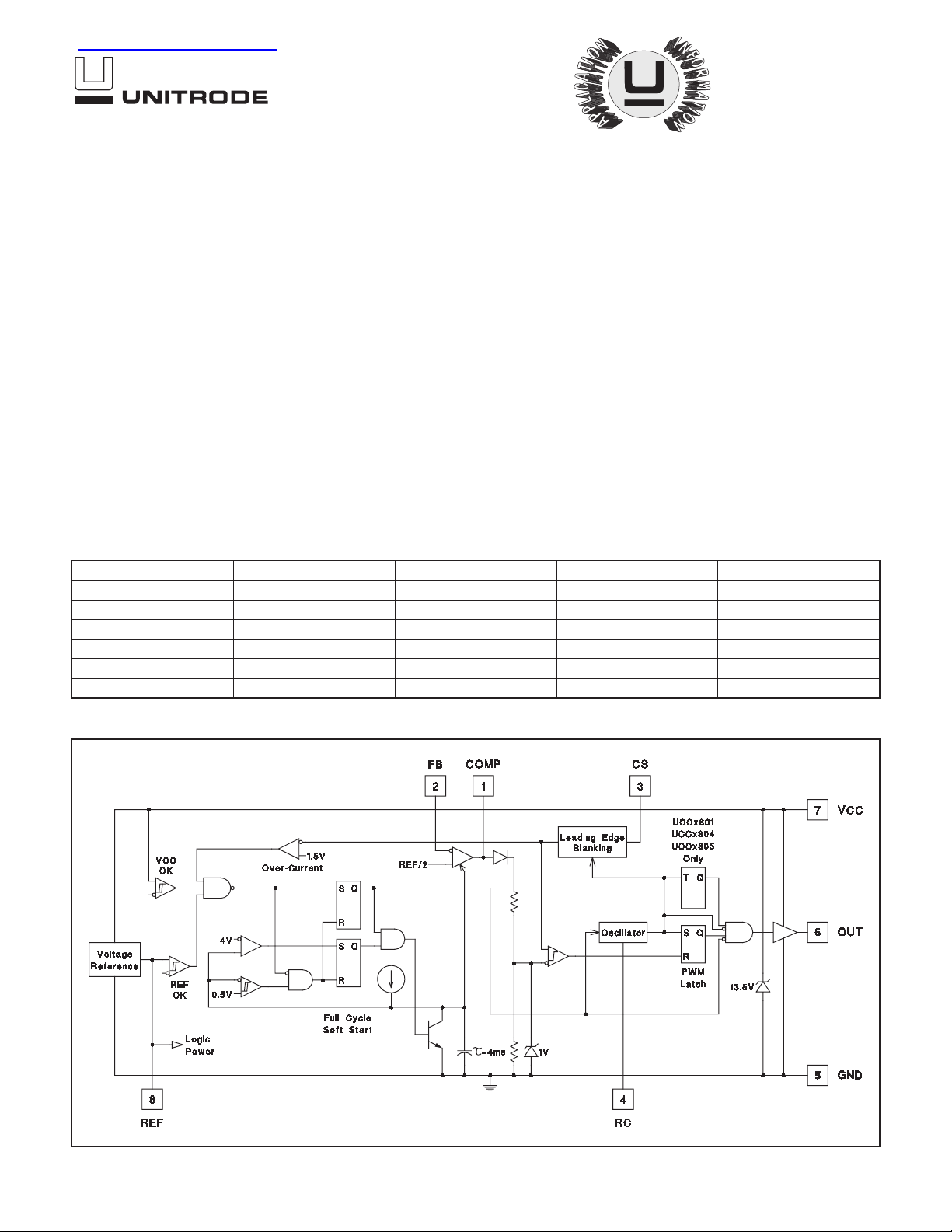
The UCC1800/1/2/3/4/5 family of high-speed, low-power integrated circuits contain all of the control and drive components required for off-line
and DC-to-DC fixed frequency current-mode switching power supplies
with minimal parts count.
These devices have the same pin configuration as the UC1842/3/4/5
family, and also offer the added features of internal full-cycle soft start
and internal leading-edge blanking of the current-sense input.
The UCC1800/1/2/3/4/5 family offers a variety of package options, tem-
• Internal Leading-Edge Blanking of the
Current Sense Signal
• 1 Amp Totem-Pole Output
perature range options, choice of maximum duty cycle, and choice of critical voltage levels. Lower reference parts such as the UCC1803 and
UCC1805 fit best into battery operated systems, while the higher reference and the higher UVLO hysteresis of the UCC1802 and UCC1804
• 70ns Typical Response from
Current-Sense to Gate Drive Output
• 1.5% Tolerance Voltage Reference
• Same Pinout as UC3842 and
make these ideal choices for use in off-line power supplies.
The UCC180x series is specified for operation from –55
the UCC280x series is specified for operation from –40
the UCC380x series is specified for operation from 0
o
Cto+85oC, and
o
C to +70oC.
UC3842A
Part Number Maximum Duty Cycle Reference Voltage Turn-On Threshold Turn-Off Threshold
UCCx800 100% 5V 7.2V 6.9V
UCCx801 50% 5V 9.4V 7.4V
UCCx802 100% 5V 12.5V 8.3V
UCCx803 100% 4V 4.1V 3.6V
UCCx804 50% 5V 12.5V 8.3V
UCCx805 50% 4V 4.1V 3.6V
o
C to +125oC,
BLOCK DIAGRAM
03/99
UDG92009-3
ABSOLUTE MAXIMUM RATINGS (Note 1)
VCCVoltage (Note 2). . . . . . . . . . . . . . . . . . . . . . . . . . . . 12.0V
VCCCurrent . . . . . . . . . . . . . . . . . . . . . . . . . . . . . . . . . 30.0mA
OUT Current. . . . . . . . . . . . . . . . . . . . . . . . . . . . . . . . . . . ±1.0A
OUT Energy (Capacitive Load) . . . . . . . . . . . . . . . . . . . 20.0µJ
Analog Inputs (FB, CS). . . . . . . . . . . . . . . . . . . . –0.3V to 6.3V
Power Dissipation at TA< +25°C (N or J Package) . . . . . 1.0W
Power Dissipation at TA< +25°C (D Package). . . . . . . . 0.65W
Storage Temperature Range. . . . . . . . . . . . . –65°C to +150°C
Lead Temperature (Soldering, 10 Seconds) . . . . . . . . +300°C
Note 1: All voltages are with respect to GND.All currents are
positive into the specified terminal. Consult Unitrode
databook for information regarding thermal specifications and limitations of packages.
Note 2: In normal operation V
is powered through a current
CC
limiting resistor.Absolute maximum of 12V applies
when V
that I
is driven from a low impedance source such
CC
does not exceed 30mA.
CC
TEMPERATURE AND PACKAGE SELECTION
Temperature Range Available Packages
UCC1800 –55°C to +125°C J
UCC2800 –40°C to +85°C N, D, PW
UCC3800 0°C to +70°C N, D, PW
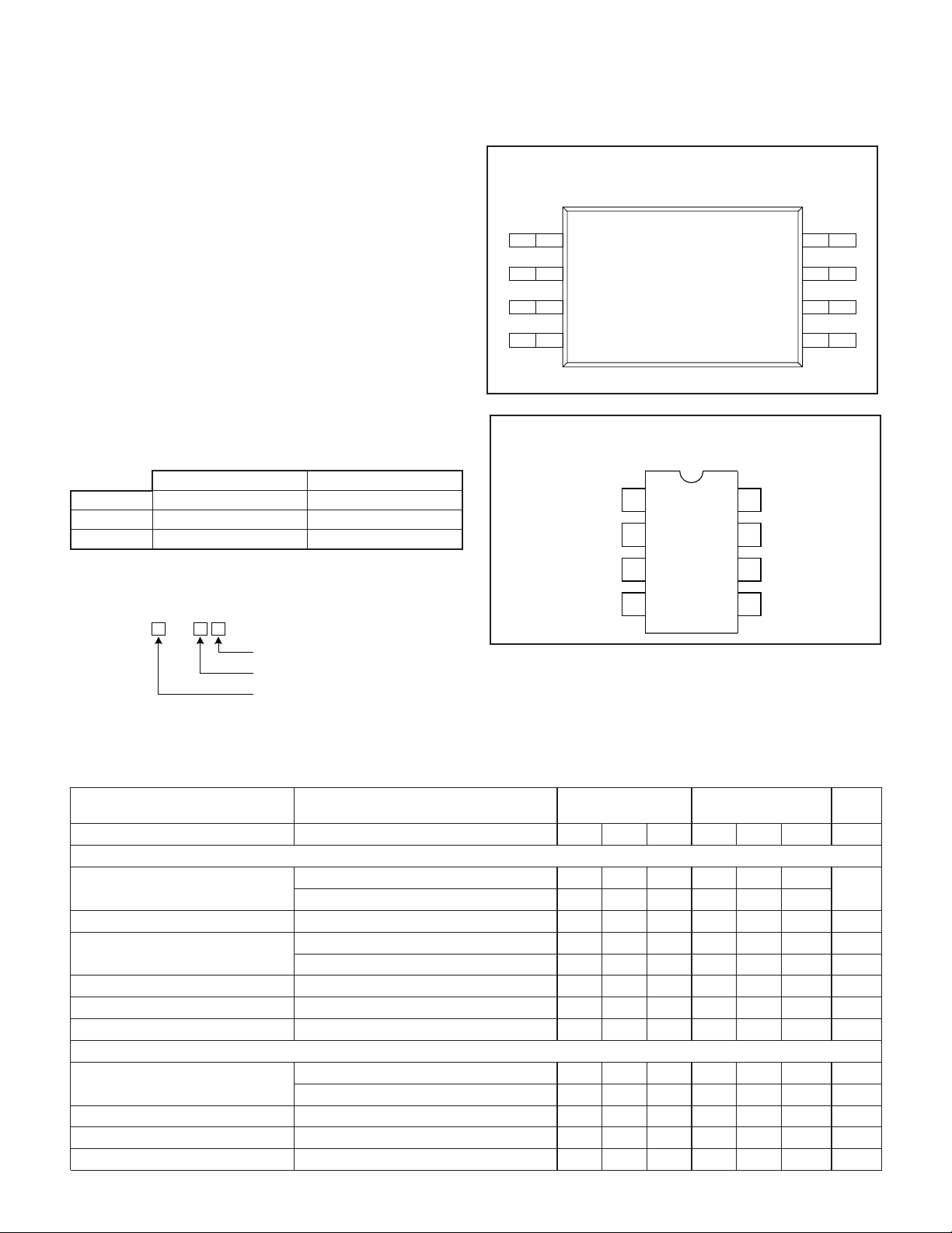
CONNECTION DIAGRAMS
TSSOP-8 (Top View)
PW Package
COMP
1
FB
2
CS
3
RC
4
DIL-8, SOIC-8 (Top View)
J or N, D Package
COMP
FB
1
2
UCC1800/1/2/3/4/5
UCC2800/1/2/3/4/5
UCC3800/1/2/3/4/5
REF
VCC
OUT
GND
8
7
8
7
6
5
REF
VCC
OUT
6
GND
5
ORDERING INFORMATION
UCC
80
CS
RC
3
4
PACKAGE
PRODUCT OPTION
TEMPERATURE RANGE
ELECTRICAL CHARACTERISTICS Unless otherwise stated, these specifications apply for –55°C ≤ T
≤ +125°C for
A
UCC180x; –40°C ≤ TA≤ +85°C for UCC280x; 0°C ≤ TA≤ +70°C for UCC380x; VCC=10V (Note 3); RT=100k from REF to RC;
CT=330pF from RC to GND; 0.1µF capacitor from VCCto GND; 0.1µF capacitor from V
PARAMETER TEST CONDITIONS UCC180X
to GND. TA=TJ.
REF
UCC380X UNITS
UCC280X
MIN TYP MAX MIN TYP MAX
Reference Section
Output Voltage T
=+25°C, I=0.2mA, UCCx800/1/2/4 4.925 5.00 5.075 4.925 5.00 5.075 V
J
=+25°C, I=0.2mA, UCCx803/5 3.94 4.00 4.06 3.94 4.00 4.06
T
J
Load Regulation 0.2mA<I<5mA 10 30 10 25 mV
Total Variation UCCx800/1/2/4 (Note 7) 4.88 5.00 5.10 4.88 5.00 5.10 V
UCCx803/5 (Note 7) 3.90 4.00 4.08 3.90 4.00 4.08 V
Output Noise Voltage 10Hz ≤ f ≤ 10kHz, T
Long Term Stability T
=+125°C, 1000 Hours (Note 9) 5 5 mV
A
=+25°C (Note 9) 130 130 µV
J
Output Short Circuit –5 –35 –5 –35 mA
Oscillator Section
Oscillator Frequency UCCx800/1/2/4 (Note 4) 40 46 52 40 46 52 kHz
UCCx803/5 (Note 4) 26 31 36 26 31 36 kHz
Temperature Stability (Note 9) 2.5 2.5 %
Amplitude peak-to-peak 2.25 2.40 2.55 2.25 2.40 2.55 V
Oscillator Peak Voltage 2.45 2.45 V
2
UCC1800/1/2/3/4/5
UCC2800/1/2/3/4/5
UCC3800/1/2/3/4/5
ELECTRICAL CHARACTERISTICS
UCC180x; –40°C ≤ TA≤ +85°C for UCC280x; 0°C ≤ TA≤ +70°C for UCC380x; VCC=10V (Note 3); RT=100k from REF to RC;
CT=330pF from RC to GND; 0.1µF capacitor from VCCto GND; 0.1µF capacitor from V
PARAMETER TEST CONDITIONS UCC180X
Error Amplifier Section
Input Voltage COMP=2.5V; UCCx800/1/2/4 2.44 2.50 2.56 2.44 2.50 2.56 V
COMP=2.0V; UCCx803/5 1.95 2.0 2.05 1.95 2.0 2.05
Input Bias Current
Open Loop Voltage Gain 60 80 60 80 dB
COMP Sink Current FB=2.7V, COMP=1.1V 0.3 3.5 0.4 2.5 mA
COMP Source Current FB=1.8V, COMP=REF–1.2V –0.2 –0.5 –0.8 –0.2 –0.5 –0.8 mA
Gain Bandwidth Product (Note 9) 2 2 MHz
PWM Section
Maximum Duty Cycle UCCx800/2/3 97 99 100 97 99 100 %
UCCx801/4/5 48 49 50 48 49 50
Minimum Duty Cycle COMP=0V 0 0 %
Current Sense Section
Gain (Note 5) 1.10 1.65 1.80 1.10 1.65 1.80 V/V
Maximum Input Signal COMP=5V (Note 6) 0.9 1.0 1.1 0.9 1.0 1.1 V
Input Bias Current
CS Blank Time 50 100 150 50 100 150 ns
Over-Current Threshold 1.42 1.55 1.68 1.42 1.55 1.68 V
COMP to CS Offset CS=0V 0.45 0.90 1.35 0.45 0.90 1.35 V
Output Section
OUT Low Level I=20mA, all parts 0.1 0.4 0.1 0.4 V
I=200mA, all parts 0.35 0.90 0.35 0.90 V
I=50mA, VCC=5V, UCCx803/5 0.15 0.40 0.15 0.40 V
I=20mA, VCC=0V, all parts 0.7 1.2 0.7 1.2 V
OUT High V
(VCC-OUT)
Rise Time C
Fall Time C
Undervoltage Lockout Section
Start Threshold (Note 8) UCCx800 6.6 7.2 7.8 6.6 7.2 7.8 V
Stop Threshold (Note 8) UCCx1800 6.3 6.9 7.5 6.3 6.9 7.5 V
Start to Stop Hysteresis UCCx800 0.12 0.3 0.48 0.12 0.3 0.48 V
SAT
I=–20mA, all parts 0.15 0.40 0.15 0.40 V
I=–200mA, all parts 1.0 1.9 1.0 1.9 V
I=–50mA,VCC=5V, UCCx803/5 0.4 0.9 0.4 0.9 V
UCCx801 8.6 9.4 10.2 8.6 9.4 10.2 V
UCCx802/4 11.5 12.5 13.5 11.5 12.5 13.5 V
UCCx803/5 3.7 4.1 4.5 3.7 4.1 4.5 V
UCCx1801 6.8 7.4 8.0 6.8 7.4 8.0 V
UCCx802/4 7.6 8.3 9.0 7.6 8.3 9.0 V
UCCx803/5 3.2 3.6 4.0 3.2 3.6 4.0 V
UCCx801 1.6 2 2.4 1.6 2 2.4 V
UCCx802/4 3.5 4.2 5.1 3.5 4.2 5.1 V
UCCx803/5 0.2 0.5 0.8 0.2 0.5 0.8 V
Unless otherwise stated, these specifications apply for –55°C ≤ TA≤ +125°C for
to GND. TA=TJ.
REF
UCC280X
UCC380X UNITS
–11–11µA
–200 200 –200 200 nA
=1nF 41 70 41 70 ns
L
=1nF 44 75 44 75 ns
L
3
 Loading...