

查询UCC1921供应商
Latchable Negative Floating Hot Swap Power Manager
UCC1921
UCC2921
UCC3921
FEATURES
• Precision Fault Threshold
• Programmable:
Average Power Limiting, Linear
Current Control, Overcurrent Limit
and Fault Time
• Fault Output Indication Signal
• Automatic Retry Mode or Latched
Operation Mode
• Shutdown Control
• Undervoltage Lockout
• 250µs Glitch Filter on the SDFLTCH
pin
• 8-Pin DIL and SOIC
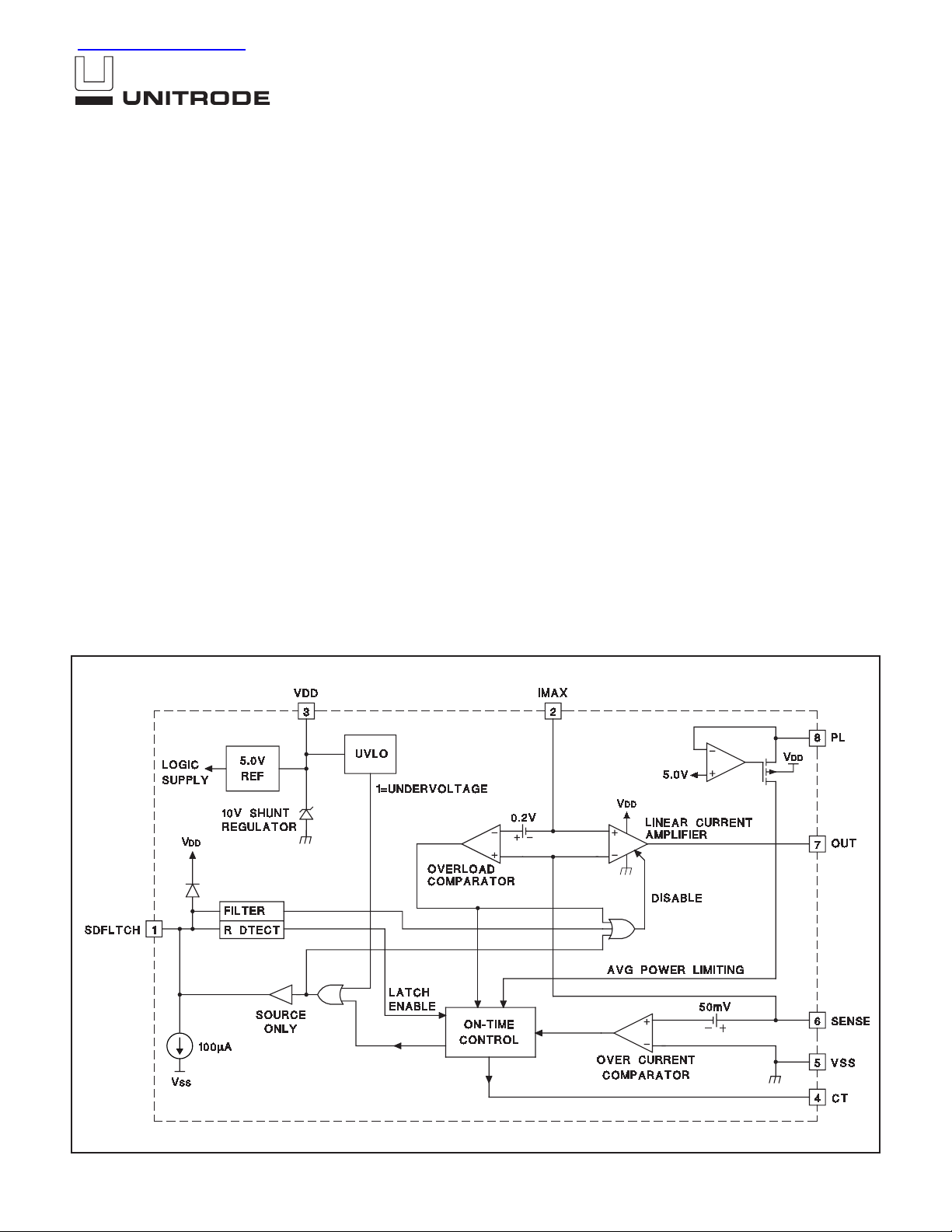
DESCRIPTION
The UCC3921 family of negative floating hot swap power managers provides complete power management, hot swap, and fault handling capability. The IC is referenced to the negative input voltage and is powered
through an external resistor connected to ground, which is essentially a
current drive as opposed to the traditional voltage drive. The onboard
10V shunt regulator protects the IC from excess voltage and serves as a
reference for programming the maximum allowable output sourcing current during a fault. All control and housekeeping functions are integrated
and externally programmable. These include the fault current level, maximum output sourcing current, maximum fault time, selection of Retry or
Latched mode, soft start time, and average power limiting. In the event of
a constant fault, the internal timer will limit the on time from less than
0.1% to a maximum of 3% duty cycle. The duty cycle modulation depends on the current into PL, which is a function of the voltage across
the FET, thus limiting average power dissipation in the FET. The fault
level is fixed at 50mV across the current sense amplifier to minimize total
(continued)
BLOCK DIAGRAM
3/98
UDG-99052
DESCRIPTION (continued)
dropout. The fault current level is set with an external
current sense resistor, while the maximum allowable
sourcing current is programmed with a voltage divider
from VDD to generate a fixed voltage on IMAX. The current level, when the output acts as a current source, is
equal to V
start up can be programmed with a capacitor on IMAX.
When the output current is below the fault level, the output device is switched on. When the output current exceeds the fault level, but is less than the maximum
sourcing level programmed by IMAX, the output remains
switched on, and the fault timer starts charging C
IMAX/RSENSE. If desired, a controlled current
T. Once
UCC1921
UCC2921
UCC3921
C
T charges to 2.5V, the output device is turned off and
performs a retry some time later (provided that the selected mode of operation is Automatic Retry Mode).
When the output current reaches the maximum sourcing
current level, the output acts as a current source, limiting
the output current to the set value defined by IMAX.
Other features of the UCC3921 include undervoltage
lockout, 8-pin Small Outline (SOIC) and Dual-In-Line
(DIL) packages, and a Latched Operation Mode option,
in which the output is latched off once C
2.5V and stays off until either SDFLTCH is toggled (for
greater than 1ms) or the IC is powered down and then
back up.
T charges to
ABSOLUTE MAXIMUM RATINGS
IVDD..........................................50mA
SDFLTCH Current ..............................10mA
PL Current ....................................10mA
IMAX Input Voltage ..............................VDD
Storage Temperature ...................−65°C to +150°C
Junction Temperature...................–55°C to +150°C
Lead Temperature (Soldering, 10 sec.) .............+300°C
All voltages are with respect to VSS(the most negative voltage).
Currents are positive into, negative out of the specified terminal.
Consult Packaging Section of Databook for thermal limitations and
considerations of packages.
ELECTRICAL CHARACTERISTICS
for the UCC2921, and –55°C to 125°C for the UCC1921; I
resistor connected between the SDFLTCH and VSS pins. TA=TJ.
PARAMETER TEST CONDITIONS MIN TYP MAX UNITS
VDD Section
IDD 12mA
Regulator Voltage I
UVLO Off Voltage 678V
Fault Timing Section
Overcurrent Threshold T
Overcurrent Input Bias 50 500 nA
CT Charge Current V
CT Discharge Current VCT= 1V, IPL= 0 0.6 1 1.5 µA
CT Fault Threshold 2.2 2.45 2.6 V
CT Reset Threshold 0.41 0.49 0.57 V
Output Duty Cycle Fault Condition, I
Unless otherwise specified, TA= 0°C to 70°C for the UCC3921 and –40°C to 85°C
= 2mA, CT= 1nF (the minimum allowable value), there is no
VDD
SOURCE
I
SOURCE
Over Operating Temperature 46 50 53.5 mV
Overload Condition, V
= 2mA 9 9.5 10.0 V
= 10mA 9.15 9.6 10.15 V
= 25°C 47.5 50 53.5 mV
J
= 1V, IPL= 0 –50 –36 –22 µA
CT
= 0 1.7 2.7 3.7 %
PL
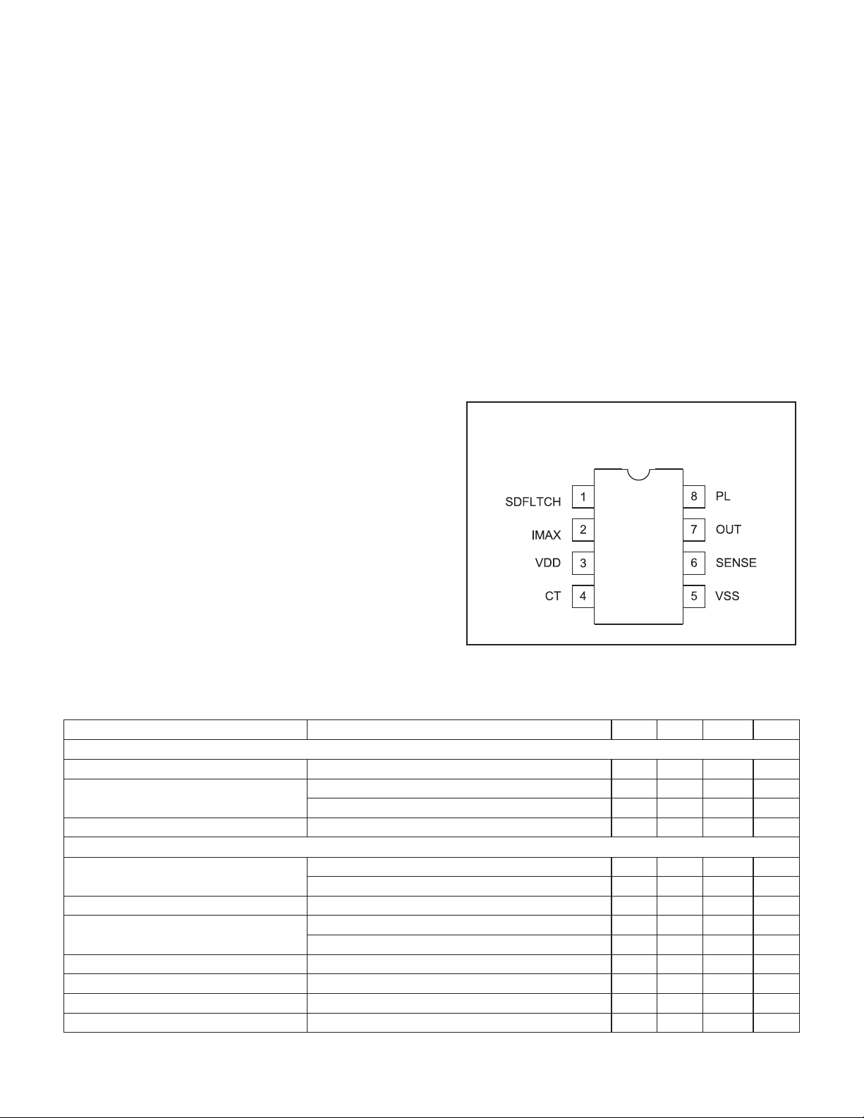
CONNECTION DIAGRAM
DIL-8 , SOIC-8 (Top View)
NorJ,DPackages
SENSE-VIMAX
= 300mV –1.7 –1.2 –0.7 mA
2
UCC1921
UCC2921
UCC3921
ELECTRICAL CHARACTERISTICS
for the UCC2921, and –55°C to 125°C for the UCC1921; I
resistor connected between the SDFLTCH and VSS pins. TA=TJ.
PARAMETER TEST CONDITIONS MIN TYP MAX UNITS
Output Section
Output High Voltage I
Output Low Voltage I
Linear Amplifier Section
Sense Control Voltage V
Input Bias 50 500 nA
Power Limiting Section
SENSE Regulator Voltage I
V
Duty Cycle Control IPL=64µA 0.6 1.2 1.7 %
Overload Section
Delay to Output Note 1 300 500 ns
Output Sink Current V
Threshold Relative to IMAX 140 200 260 mV
Shutdown/Fault/Latch Section
Shutdown Threshold 3 5 VDD+1 V
Input Current V
Filter Delay Time (Delay to Output) 250 500 1000 µs
Fault Output High 6 9.5 V
Fault Output Low 010mV
Output Duty Cycle Fault Condition, I
Unless otherwise specified, TA= 0°C to 70°C for the UCC3921 and –40°C to 85°C
= 2mA, CT= 1nF (the minimum allowable value), there is no
VDD
= 0mA 8.5 10 V
OUT
I
= –1mA 6 8 V
OUT
= 0mA, V
OUT
I
= 2mA, V
OUT
= 100mV 85 100 115 mV
IMAX
= 400mV 370 400 430 mV
V
IMAX
=64µA 4.35 4.85 5.35 V
PL
IPL= 1mA 0.045 0.1 0.17 %
SENSE–VIMAX
SDFLTCH
I
SDFLTCH
I
SDFLTCH
SENSE–VIMAX
SENSE–VIMAX
= 300mV 40 100 mA
= 5V 50 110 250 µA
= –100µA 5 8.5 V
= 0 1.7 2.7 3.7 %
PL
= –100µA, Fault Condition, IPL=0 0 %
= 100mV 0 10 mV
= 100mV 200 600 mV
Note 1: Guaranteed by design. Not 100% tested in production.
PIN DESCRIPTIONS
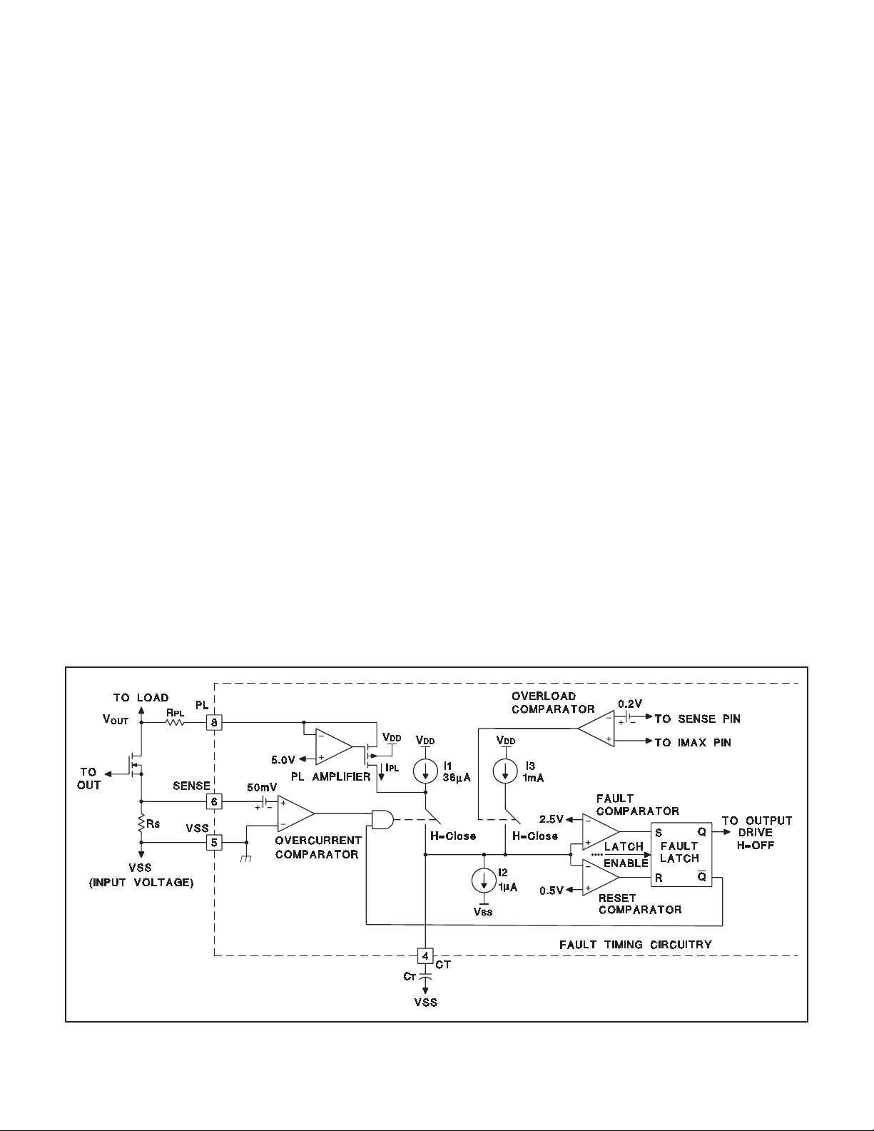
CT: A capacitor is connected to this pin in order to set
the fault time. The fault time must be longer than the time
to charge external load capacitance. The fault time is
defined as:
C
•
2
T
FAULT
where ICH =36µA+IPL, and IPL is the current into the
power limit pin. Once the maximum fault time is reached
the output will shutdown for a time given by:
=• •
210
TC
SD T
IMAX: This pin programs the maximum allowable
sourcing current. Since VDD is a regulated voltage, a
voltage divider can be derived from VDD to generate the
program level for IMAX. The current level at which the
output appears as a current source is equal to the
T
=
I
CH
6
voltage on IMAX over the current sense resistor. If
desired, a controlled current start up can be programmed
with a capacitor on IMAX, and a programmed start delay
can be achieved by driving the shutdown with an open
collector/drain device into an RC network.
OUT: This pin provides gate output drive to the MOSFET
pass element.
PL: This feature ensures that the average MOSFET
power dissipation is controlled. A resistor is connected
from this pin to the drain of the NMOS pass element.
When the voltage across the NMOS exceeds 5V, current
will flow into the PL pin which adds to the fault timer
charge current, reducing the duty cycle from the 3%
level. When I
>>36µA, then the average MOSFET
PL
power dissipation is given by:
−
P avg IMAX R
MOSFET PL
=•••
110
6
3
PIN DESCRIPTIONS (continued)
SENSE: Input voltage from the current sense resistor.
When there is greater than 50mV across this pin with
respect to VSS, then a fault is sensed, and C
charge.
SDFLTCH: This pin provides fault output indication,
shutdown control, and operating mode selection.
Interface into and out of this pin is usually performed
through level shift transistors. When open, and under a
non-fault condition, this pin pulls to a low state with
respect to VSS. When a fault is detected by the fault
timer, or undervoltage lockout, this pin will drive to a high
state with respect fo VSS, indicating the NMOS pass
element is OFF. When > 250µA is sourced into this pin
for > 1ms, it drives high causing the output to disable the
NMOS pass device.
starts to
T
UCC1921
UCC2921
UCC3921
If an 5k < R
to VSS, then the latched operating mode will be invoked.
Upon the occurrence of a fault, under the latched mode
of operation, once the C
the NMOS pass element latches off. A retry will not
periodically occur. To reset the latched off device, either
SDFLTCH is toggled high for a duration greater than 1ms
or the IC is powered down and then up.
VDD: Current driven with a resistor to a voltage approximately 10V more positive than VSS. Typically a resistor is
connected to ground. The 10V shunt regulator clamps
VDD approximately 10V above VSS, and is also used as
an output reference to program the maximum allowable
sourcing current.
VSS: Ground reference for the IC and the most negative
voltage available.
< 250kΩ resistor is placed from this pin
LATCH
capacitor charges up to 2.5V
T
APPLICATION INFORMATION
Figure 1. Fault Timing Circuitry for the UCC3921, Including Power Limit Overload
UDG-96275-1
4
 Loading...