

UNITRODE UCC1890, UCC2890, UCC3890 Technical data
查询UCC1890供应商
Off-Line Battery Charger Circuit
UCC1890
UCC2890
UCC3890
FEATURES
• Transformerless Off-Line
Operation
• Low Voltage Operation to 0.8V
• Ideal for Battery Trickle Charger
Applications
• Current Mode Operation With
100mV Shunt
• Voltage Mode Operation With
Fixed 1.25V Output or Resistor
Adjustable Output
• Efficient BiCMOS Design
• Inherent Short Circuit Protection
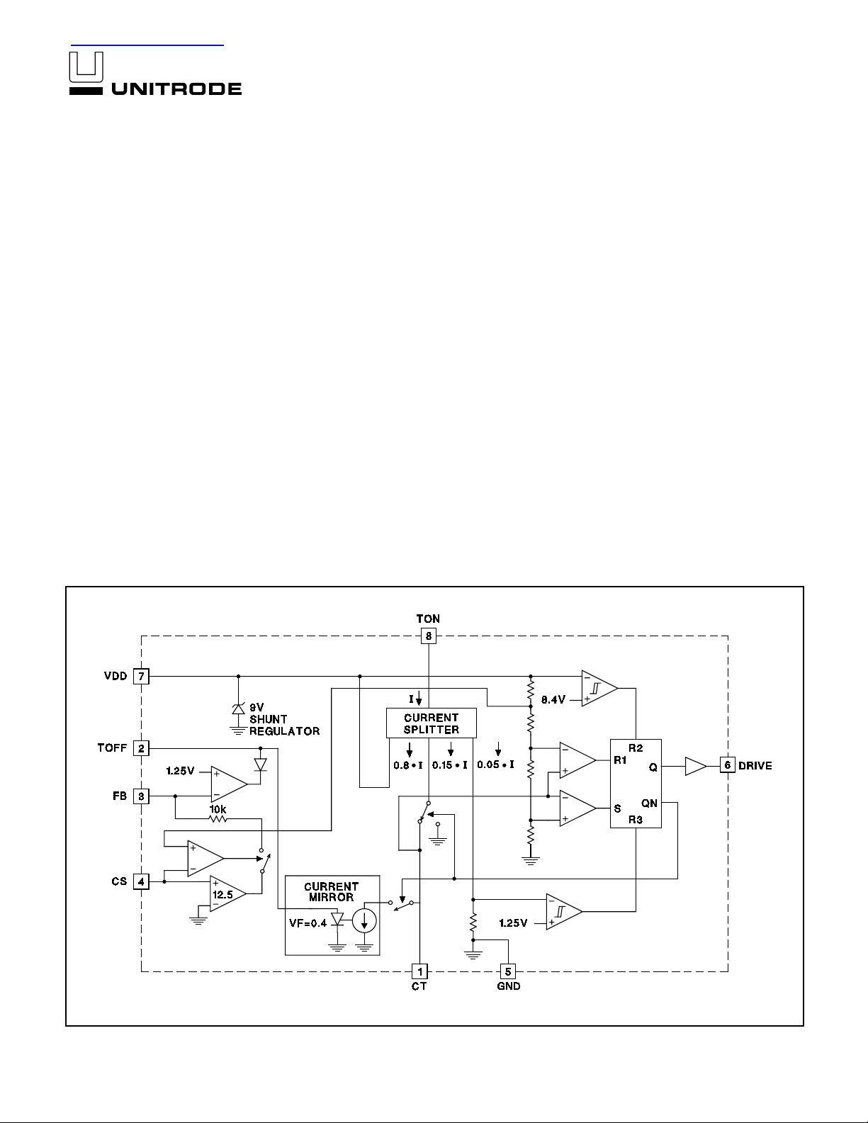
BLOCK DIAGRAM
DESCRIPTION
The UCC3890 controller is optimized for use as an off-line, low power, low
voltage, regulated current supply, ideally suited for battery trickle charger
applications. The unique circuit topology used in this device can be visualized as two cascaded flyba ck converters; each operating in the discontinuous mode, and both driven from a s ingle external power switch. The
significant benefit of this approach is the ability to charge low voltage batteries in off-line applications with no transformer, and low internal losses.
The control algorithm used by the UCC3890 forces a switch on time inversely pr oportional to t he input line v oltage, whil e the switch off time is
inversely proportional to the output voltage. This action is automatically
controlled by an internal fe ed ba c k l oo p a nd reference. The cascaded c onfiguration al lows a large voltage c onversion ratio with r easonable switch
duty cycle.
While the UCC3890 is ideally suited for control of constant current battery
chargers, provision is also made to operate as a fixed 1.25V regulated
supply, or to use a resistor vo l tage di vi der to obtain output vol tages hi gher
than 1.25V.
Note: This device incorporates patented technology used under license from
Lambda Electronics, Inc.
3/97
UDG-96052
UCC1890
UCC2890
UCC3890
ABSOLUTE MAXIMUM RATINGS
IDD . . . . . . . . . . . . . . . . . . . . . . . . . . . . . . . . . . . . . . . . . . 7.5mA
Current into TON . . . . . . . . . . . . . . . . . . . . . . . . . . . . . . . 7.5mA
Voltage on V
OUT . . . . . . . . . . . . . . . . . . . . . . . . . . . . . . . . . . . . . . . . . . .
20V
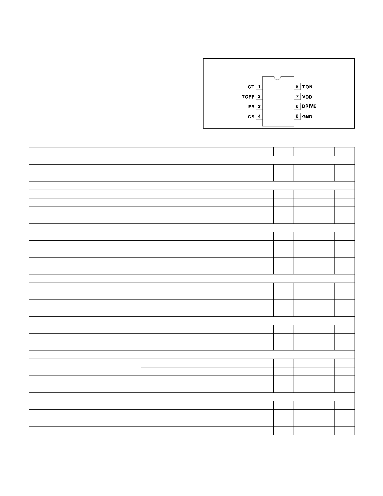
CONNECTION DIAGRAMS
DIL-8, SOIC-8 (Top View)
J, N, or D Packages
Current into TOFF . . . . . . . . . . . . . . . . . . . . . . . . . . . . . . 250µA
Storage Temperature . . . . . . . . . . . . . . . . . . . –65°C to +150°C
Junction Temperature . . . . . . . . . . . . . . . . . . –55°C to +150°C
Lead Temperature (Soldering, 10 sec.) . . . . . . . . . . . . . +300°C
Currents are positive into, negative out of the specified terminal.
Consult Packaging Section of Databook for thermal limitations
and considerations of packages.
ELECTRICAL CHARACTERISTICS:
UCC1890, –40°C to 85°C for the UCC2890, and 0°C to 70°C for the UCC3890. No load at DRIVE pin (C
Unless otherwise stated, these specifications apply for TA = –55°C to 125°C for
= 0), TA = TJ.
LOAD
PARAMETER TEST CONDITIONS MIN TYP MAX UNITS
General
VDD Zener Voltage I
Minimum Operat in g C urre nt I
TON
= 4.75mA,I
DD
= 0mA 8.3 9.0 9.4 V
TON
IDD = –1mA, F = 150kHz 1.65 2.0 mA
Undervoltage Lockout
Minimum Voltage to Start FB = 0 7.8 8.6 9.2 V
Minimum Voltage after Start FB = 0 5.75 6.3 6.65 V
Hysteresis FB = 0 1.8 2.3 2.6 V
VDD – V
START
FB = 0 0.2 0.4 0.7 V
Oscillator
Amplitude I
TON
= 3mA; I
= 50µA; VFB = 0V CT = 100pF 3.1 3.4 3.7 V
TOFF
CT to DRIVE High Delay Overdrive = 200mV 80 200 ns
CT to DRIVE Low Delay Overdrive = 200mV 50 100 ns
Charge Coefficient I
CT/ITON
Discharge Coefficent I
CT/ITOFF
I
= 3mA; V
TON
I
= 50µA; VCT = 3.0V 0.95 1.00 1.05µA/µA
TOFF
= 3.0V 0.135 0.15 0.165µA/µA
CT
Driver
V
OL
V
OH
Rise Time C
Fall Time C
I = 100mA (Note 1) 0.7 1.8 V
I = –100mA referred to VDD (Note 1) –2.9 –1.5 V
= 1nF 35 70 ns
L
= 1nF 30 60 ns
L
Line Voltage Detection
Minimum I
Detector Hysteresis 110
TON
I
for Fault 1.0 1.5 2.0 mA
TON
On Time During Fault 0.5
OUT
V
Error Amplifier
Reference Level I
Voltage at TOFF I
Regulation gm I
= 50µA, ICT = 25µA, TJ = 25°C 1.20 1.25 1.30 V
TOFF
= 50µA, ICT = 25µA, Over Temperature 1.15 1.25 1.35 V
TOFF
I
= 50µA 0.3 0.4 0.5 V
TOFF
= 50µA (Note 2) 2.0 4.0 7.7 mA/V
TOFF
Current Sense Amplifier
Gain VCS = 90 – 110mV 11.8 12. 5 13.0 V/V
Input Offset Voltage V
Input Voltage for CS Amplifier Enabled I
Input Voltage for CS Amplifier Disabled I
= 90 – 110mV –5 0 5 mV
CS
= 3mA, Referred to VDD –1.5 –0.8 V
TON
= 3mA, Referred to VDD –0.8 –0.3 V
TON
µ
A
µ
s
Note 1: VDD forced to 100mV below VDD Zener Voltage
∆
CT
Note 2: gm is defined as
are for I
at 65% amd 35% of its maximum value.
CT
I
for the values of VFB where the error amp is in regulation. The two points used to calculate gm
∆
FB
V
2
PIN DESCRIPTIONS
CS:
The high side of the current sense shunt is connected to this pi n. Short CS to VDD for voltage feedback
operation.
UCC1890
UCC2890
UCC3890
TOFF:
Resistor R
this pin to provide a maximum capacitor discharge current proportional to output voltage.
OFF
connects from voltage output to
CT:
Oscillator timing capacitor is connected to this pin.
DRIVE:
FB:
Gate drive to external power switch.
Output of current sense amplifier. This pin can be
used for direct output voltage feedback if the current
sense amp input pin CS is shorted to the VDD pin.
GND:
Ground pin.
APPLICATION INFORMATION
TON:
Resistor R
ON
connects f rom lin e in put to this pin to
provide capacitor charge current proportional to line voltage. The current in R
ON
also provides power for the 9V
shunt regulator at VDD.
VDD:
Output of 9V shunt regulator.
Figure 1. Typical Voltage Mode Application
OPERATION (VOLTAGE OUTPUT)
Figure 1 shows a typical voltage mode application.
When input voltage is first applied, all of the current
through R
DD
and 80% of the current through R
ON,
charge the ext ernal ca paci tor C3 conn ected to VDD. As
the volta ge builds on VDD, u ndervoltage lockout holds
the circuit off and the output DRIVE low until VDD
reaches 8.4 V. At this time, DRI VE go es h igh, turning on
the external power switch Q1, and 15% of the current
into TON is directed to the timing capacitor C
T
. The voltage at TON is fixed at approximately 11V, so C
charges to a fixed threshold with current
IN
V
I = 0.2 •
– 11V
ON
R
Since the input line is much greater than 11V, the
charge current is approximately proportional to the input
T
line voltage. DRIVE is only high while C
is charging, so
the power swi tc h on time i s inver sely pr oportional to l ine
voltage. Thi s provides a constant line voltage-switch on
time product.
At the end of the switc h on time, Q1 i s turned off, and
ON
the 15% of the R
current which was charging CT is
diverted to ground . The power switch off time is controlled by discharge of C
T
, which is determined by the outut
voltage as described here:
T
3
UDG-96053
UDG-96054
 Loading...