

UNITRODE UCC1810, UCC2810, UCC3810 Technical data
查询UCC1810供应商
Dual Channel Synchronized Current Mode PWM
UCC1810
UCC2810
UCC3810
FEATURES
• Single Oscillator Synchronizes Two
PWMs
• 150
• 2mA Operating Supply Current
• Operation to 1MHz
• Internal Soft Start
• Full-Cycle Fault Restart
• Internal Leading Edge Blanking of the
• 1 Amp Totem Pole Outputs
• 75ns Typical Response from Current
• 1.5% Tolerance Voltage Reference
A Startup Supply Current
Current Sense Signal
Sense to Output
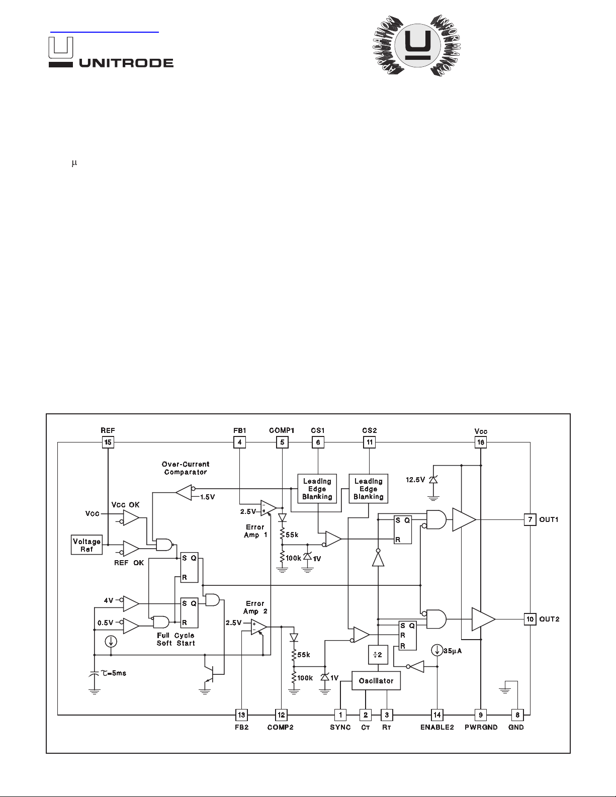
BLOCK DIAGRAM
DESCRIPTION
The UCC3810 is a high-speed BiCMOS integrated circuit which implements two synchronized pulse width modulators for use in off-line and
DC-to-DC power supplies.
The UCC3810 provides perfect synchronization between two PWMs by using the same oscillator. The oscillator’s sawtooth waveform can be used for
slope compensation if required.
Using a toggle flip flop to alternate between modulators, the UCC3810 ensures that one PWM will not slave, interfere, or otherwise affect the other
PWM. This toggle flip flop also ensures that each PWM will be limited to
50% maximum duty cycle, insuring adequate off-time to reset magnetic elements.
This IC contains many of the same elements of the UC3842 current mode
controller family, combined with the enhancements of the UCC3802. This
minimizes power supply parts count. Enhancements include leading edge
blanking of the current sense signals, full cycle fault restart, CMOS output
drivers, and outputs which remain low even when the supply voltage is removed.
02/99
UDG-92062-1
ABSOLUTE MAXIMUM RATINGS
VCCVoltage (Note 3). . . . . . . . . . . . . . . . . . . . . . . . . . . . . . 11V
VCCCurrent . . . . . . . . . . . . . . . . . . . . . . . . . . . . . . . . . . . 20mA
OUT1, OUT2 Current, Peak, 5% Duty Cycle. . . . . . . . . . . .±1A
OUT1, OUT2 Energy (Capacitive Load) . . . . . . . . . . . . . . 20µJ
Analog Inputs (FB1, FB2, CS1, CS2, SYNC). . . . –0.3V to 6.3V
Operating Junction Temperature. . . . . . . . . . . . . . . . . . +150°C
Storage Temperature Range . . . . . . . . . . . . . –65°C to +150°C
Lead Temperature (Soldering, 10 seconds) . . . . . . . . . . 300°C
UCC1810
UCC2810
UCC3810
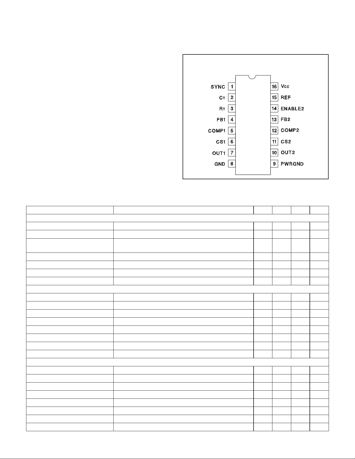
CONNECTION DIAGRAM
DIL-16, SOIC-16 (TOP VIEW)
J or N Package, DW Package
Note 1: All voltages are with respect to GND. All currents are
positive into the specified terminals.
Note 2: Consult Unitrode Integrated Circuits Product & Appli-
cations Handbook for information regarding thermal
specifications and limitations of packages.
Note 3: In normal operation, V
is powered through a current
CC
limiting resistor. Absolute maximum of 11V applies
when driven from a low impedance such that the V
CC
current does not exceed 20mA.
ELECTRICAL CHARACTERISTICS:
UCC1810; –40°C≤T
85°C for UCC2810; 0°C≤T
≤
A
Unless otherwise stated, these specifications apply for –55°C≤T
70°C for UCC3810; V
≤
A
= 10V (Note 4); RT= 150k; CT= 120pF;
CC
125°C for
≤
A
No Load; TA= TJ. All parameters are the same for both channels.
PARAMETER TEST CONDITIONS MIN TYP MAX UNITS
Reference Section
Output Voltage T
Load Regulation 0mA < I
Line Regulation UVLO Stop Threshold Voltage +0.5V < VCC< Shunt
= 25°C 4.925 5.000 5.075 V
J
< 5mA 5 25 mV
REF
12 mV
Voltage
Output Voltage Full temperature range, 0mA < I
< 5mA 4.85 5.00 5.10 V
REF
Output Noise Voltage 10Hz < f < 10kHz, TJ= +25°C (Note 10) 235 µV
Long Term Stability TA= +125°C, 1000 Hours (Note 10) 5 mV
Output Short Circuit Current –8 –25 mA
Oscillator Section
Oscillator Frequency R
= 30k, CT= 120pF (Note 5) 840 940 1040 kHz
T
Oscillator Frequency RT= 150k, CT= 120pF (Note 5) 200 220 240 kHz
Temperature Stability (Note 10) 2.5 %
Peak Voltage 2.5 V
Valley Voltage 0.05 V
Peak-to-Peak Amplitude 2.25 2.45 2.65 V
SYNC Threshold 0.80 1.65 2.2 V
SYNC Input Current SYNC = 5V 30 µA
Error Amplifier Section
FB Input Voltage COMP = 2.5V 2.44 2.50 2.56 V
FB Input Bias Current ±1 µA
Open Loop Voltage Gain 60 73 dB
Unity Gain Bandwidth (Note 10) 2 MHz
COMP Sink Current FB = 2.7V, COMP = 1V 0.3 1.4 3.5 mA
COMP Source Current FB = 1.8V, COMP = 4V –0.2 –0.5 –0.8 mA
Minimum Duty Cycle COMP = 0V 0 %
COMP Soft Start Rise Time FB = 1.8V, Rise from 0.5V to REF–1.5V 5 ms
2
UCC1810
UCC2810
UCC3810
ELECTRICAL CHARACTERISTICS:
UCC1810; –40°C≤T
85°C for UCC2810; 0°C≤T
≤
A
Unless otherwise stated, these specifications apply for –55°C≤T
70°C for UCC3810; VCC= 10V (Note 4); RT= 150k; CT= 120pF;
≤
A
125°C for
≤
A
No Load; TA= TJ. All parameters are the same for both channels.
PARAMETER TEST CONDITIONS MIN TYP MAX UNITS
Current Sense Section
Gain (Note 6) 1.20 1.55 1.80 V/V
Maximum Input Signal COMP = 5V (Note 7) 0.9 1.0 1.1 V
CS Input Bias Current
±
200 nA
CS to OUT Propagation Delay CS steps from 0V to 1.2V, COMP = 2.5V 75 ns
CS Blank Time (Note 8) 55 ns
CS Overcurrent Threshold 1.35 1.55 1.85 V
COMP to CS Offset CS = 0V 0.65 0.95 1.4 V
PWM Section
Maximum Duty Cycle R
T = 150k, CT = 120pF (Note 10) 45 49 50 %
Maximum Duty Cycle RT = 30k, CT = 120pF (Note 10) 40 45 48 %
Minimum On Time CS =1.2V, COMP = 5V 130 ns
Output Section
OUT Low Level I
OUT = 20mA 0.12 0.42 V
IOUT = 200mA 0.48 1.10 V
IOUT = 20mA, VCC = 0V 0.7 1.20 V
OUT High Level
(VCC - OUT)
OUT Rise Time C
IOUT = –20mA 0.15 0.42 V
IOUT = –200mA 1.20 2.30 V
OUT = 1nF 20 50 ns
OUT Fall Time COUT = 1nF 30 60 ns
Undervoltage Lockout Section
Start Threshold 9.9 11.3 13.2 V
Stop Threshold 7.5 8.3 9.5 V
Start to Stop Hysteresis 1.7 3.0 4.7 V
ENABLE2 Input Bias Current ENABLE2 = 0V –20 –35 –55 µA
ENABLE2 Input Threshold
0.80 1.53 2.00 V
Voltage
Overall Section
Startup Current V
Operating Supply Current,
CC < Start Threshold Voltage 0.15 0.25 mA
VCC = 10V, FB = 2.75V 2.0 3.0 mA
Outputs Off
Operating Supply Current,
CC = 10V, FB = 0V, CS = 0V, RT = 150k 3.2 5.1 mA
V
Outputs On
Operating Supply Current,
CC = 10V, FB = 0V, CS = 0V, RT = 30k 8.5 14.5 mA
V
Outputs On
CC Internal Zener Voltage ICC = 10mA (Note 9) 11.0 12.9 14.0 V
V
VCC Internal Zener Voltage Minus
0.4 1.2 V
Start Threshold Voltage
Note 4: Adjust VCCabove the start threshold before setting at 10V.
Note 5: Oscillator frequency is twice the output frequency.
VCOMP
Note 6: Current Sense Gain A is defined by:
∆
A
=≤≤
VCS
∆
F
OSC
008.
4
≈
RT CT
×
VCS V
.
Note 7: Parameter measured at trip point of latch with FB = 0V.
Note 8: CS Blank Time is measured as the difference between the minimum non-zero on-time and the CS to OUT delay.
Note 9: Start Threshold Voltage and V
Internal Zener Voltage track each other.
CC
Note 10: Guaranteed by design. Not 100% tested in production.
3
 Loading...