

Quad FET Driver
UCC1776
UCC2776
UCC3776
PRELIMINARY
FEATURES
• High Peak Output Current
Each Output – 1.5A Source,
2.0A Sink
• Wide Operating Voltage
Range 4.5V to 18V
• Thermal Shutdown
• CMOS Compatible Inputs
• Outputs Are Active Low
for Undervoltage Lockout
Condition
DESCRIPTION
The UCC3776 is a four output BCDMOS buffer/driver designed to drive highly
capacitive loads such as power MOSFET gates at high speeds. The device
can be configured as either an inverting or non-inverting driver via the POL
pin.The outputs are enabled by ENBL.When disabled, all outputs are active
low. The device incorporates thermal shutdown with hysteresis for stability.
The device also includes an undervoltage lockout circuit (UVLO) with hysteresis which disables the outputs when VDD is below a preset threshold. The
outputs are held low during undervoltage lockout, even in the absence of
VDD power to the device.This helps prevent MOSFET turn-on due to capacitive current through the gate-drain capacitance of the power MOSFET in the
presence of high dV/dts. The logic input thresholds are compatible with
standard 5V HCMOS logic.
3/97
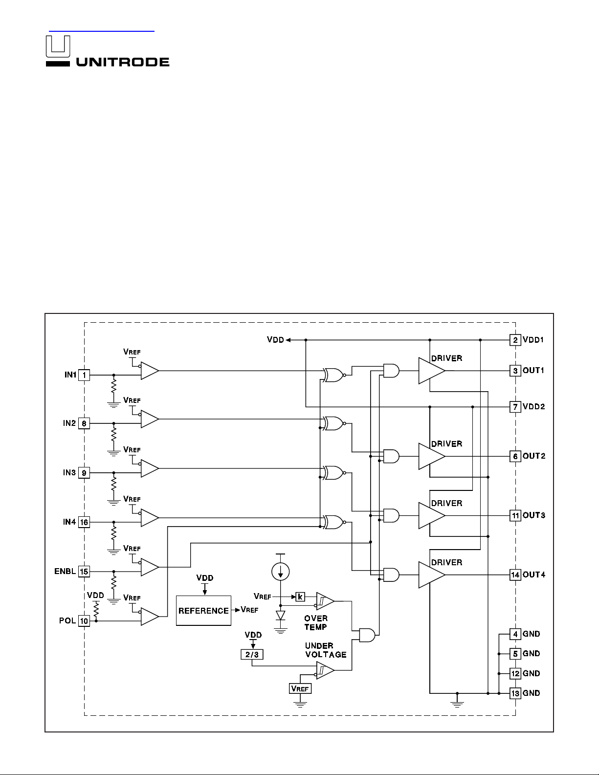
BLOCK DIAGRAM
UDG-95129-2
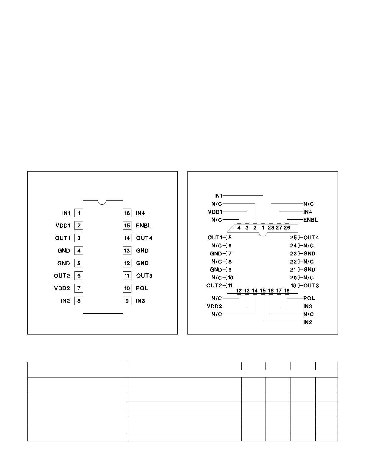
Note:Pin connections shown refer to 16-pin packages.
1
查询UCC1776供应商
2
UCC1776
UCC2776
UCC3776
ABSOLUTE MAXIMUM RATINGS
Input Supply Voltage, VDD1, VDD2 . . . . . . . . . . . . . . . . . . . . . . . . . . . . . . . . . . . . .20V
Maximum DC Voltage Difference, VDD1 vs.VDD2 . . . . . . . . . . . . . . . . . . . . . . .100mV
Logic Input, IN1, IN4, ENBL
Maximum forced voltage . . . . . . . . . . . . . . . . . . . . . . . . . . . . . .−0.3 to VDD1 + 0.3V
Logic Inputs, IN2, IN3, POL
Maximum forced voltage . . . . . . . . . . . . . . . . . . . . . . . . . . . . . .−0.3 to VDD2 + 0.3V
Latch-up Protection withstand Reverse Current
IREV, OUT1, OUT2, OUT3, OUT4 . . . . . . . . . . . . . . . . . . . . . . . . . . . . . . . . .500mA
Power Outputs, OUT1, OUT2, OUT3, OUT4
Maximum pulsed current (10% duty max, 10µsec max pulse width) . . . . . . . . . .3A
Storage Temperature . . . . . . . . . . . . . . . . . . . . . . . . . . . . . . . . . . . . . .−65°C to +150°C
Operating Junction Temperature . . . . . . . . . . . . . . . . . . . . . . . . . . . . .−55°C to +150°C
Lead Temperature (Soldering, 10 Seconds) . . . . . . . . . . . . . . . . . . . . . . . . . . . . .300°C
All currents are positive into, negative out of the specified terminal.Consult Packaging
Section of Databook for thermal limitations and considerations of packages.
CONNECTION DIAGRAMS
DIL-16 (Top View)
N or J,DP Packages
PLCC-28 (Top View)
Q Package
ELECTRICAL CHARACTERISTICS Unless otherwise stated these specifications apply for TA = −55°C to +125°C for
UCC1776;−40°C to +85°C for UCC2776;0°C to +70°C for UCC3776;VPOL = 5V, VENBL = 5V, 4.5V <VDD < 18V, TJ = TA.
PARAMETER TEST CONDITIONS MIN TYP MAX UNITS
Input Section
VIH, Logic 1 Input Voltage 3 V
VIL, Logic 0 Input Voltage 2 V
IINn, Input Current VINn = 5V 30 µA
VINn = 0V –1 +1 µA
ENBL Input Current VENBL = 5V 30 µA
VENBL = 0V –1 +1 µA
POL Input Current VPOL = 5V −1 +1 µA
V
POL = 0V −30 µA
3
UCC1776
UCC2776
UCC3776
Note 1:Guaranteed by design.Not 100% tested in production.
ELECTRICAL CHARACTERISTICS (cont.) Unless otherwise stated these specifications apply for TA = −55°C to +125°C
for UCC1776;−40°C to +85°C for UCC2776;0°C to +70°C for UCC3776;VPOL = 5V, VENBL = 5V , 4.5V <VDD < 18V, TJ = TA.
PARAMETERTEST CONDITIONS MIN TYP MAX UNITS
Output Section
VOH, High Output Voltage IOUTn = -10mA, VDD1 = VDD2= 12V, VINn = 5V VDD− 1.0 V
VOL, Low Output Voltage IOUTn = 10mA, VDD1 = VDD2 = 12V, VINn = 0V 0.15 V
Output Resistance IOUTn = 10mA, VDD1 = VDD2 = 12V, VINn = 0V 6 Ω
Output High Peak Current VDD1 = VDD2 = 12V, OUTn = 5V, V
INn = 5V, −1.5 A
TJ = 25°C (Note 1)
Output Low Peak Current VDD1 = VDD2 = 12V, OUTn = 5V, V
INn = 0V, 2.0 A
TJ = 25°C (Note 1)
UVLO Output Pull-down Voltage VDD1 = VDD2 = 3V, IOUTn = −10mA 0.8 1.5 V
Switching Time Section
Output Rise Time C
OUTn = 1nF, VOUTn = 1V to 9V,
VDD1 = VDD2 = 12V 25 50 nsec
Output Fall Time C
OUTn = 1nF, VOUTn = 9V to 1V,
VDD1 = VDD2 = 12V 10 50 nsec
IN−>OUT Delay Time (Rising Output) V
INn = 2.5V, VOUTn = 0.1 • VDD, 40 100 nsec
VDD1 = VDD2 = 12, COUTn = 0nF
IN−>OUT Delay Time (Falling Output) V
INn = 2.5V, VOUTn = 0.9 • VDD, 50 100 nsec
VDD1 = VDD2 = 12V, COUTn = 0nF
Power Supply Section
Power Supply Current V(IN1−IN4) = 0V, V
ENBL = 0V, 2 mA
VDD1 = VDD2 = 12V
UVLO Threshold 4.5 V
UVLO Hysteresis 0.5 V
ENBL: Logic level input to enable the drivers.When ENBL
is low, the drivers outputs will be at GND potential, regardless of the status of POL.The input threshold is designed
to be 5 volt CMOS compatible, independent of the VDD
voltage used on the device.There is a slight hysteresis in
the input circuit to help reduce sensitivity to noise on the
input signal or input ground.
GND: Ground for the device, the supply return for the
VDDs. There are four GND pads on the device.
IN1 - IN4: Inputs to each driver (1-4).The input threshold
is designed to be 5 volt CMOS compatible, independent
of the VDD voltage used on the device.There is a slight
hysteresis in the input circuit to help reduce sensitivity
to noise.
OUT1 - OUT4: Outputs to each driver (1-4). The outputs
are totem pole DMOS circuits. In the absence of VDD on
the device, the outputs will stay off, even with a capacitive
displacement current into the output node.
POL: Polarity selection for the drivers. A logic 0 selects
inverting operation. A logic 1 selects non-inverting operation. The input threshold is designed to be 5 volt CMOS
compatible, independent of the VDD voltage used on the
device.There is a slight hysteresis in the input circuit to
help reduce sensitivity to noise.
VDD1: Supply Voltage for drivers 1 and 4. Tied inter nally
to VDD2.
VDD2: Supply Voltage for drivers 2 and 3.Tied internally
to VDD1.
PIN DESCRIPTIONS
APPLICATION INFORMATION
Figure 1 depicts a block diagram of the UCC3776 Quad
FET Driver. Four high current, high speed gate drivers
with CMOS compatible input stages are provided.
Polar ity select and enable inputs provide circuit integra-
tion flexibility, while power packaging and high speed
drive circuitry allow for driving high power MOSFET
gates in high speed applications.
 Loading...