


查询UCC1583J供应商
Switch Mode Secondary Side Post Regulator
UCC1583
UCC2583
UCC3583
FEATURES
• Precision Secondary Side Post
Regulation for Multiple Output Power
Supplies
• Useful for Both Single Ended and
Center Tapped Secondary Circuits
• Ideal Replacement for Complex
Magnetic Amplifier Regulated Circuits
• Leading Edge Modulation
• Does Not Require Gate Drive
Transformer
• High Frequency (>500kHz) Operation
• Applicable for Wide Range of Output
Voltages
• High Current Gate Driver (0.5A
Sink/1.5A Source)
• Average Current Limiting Loop
DESCRIPTION
The UCC3583 is a synchronizable secondary side post regulator for precision regulation of the auxiliary outputs of multiple output power supplies. It
contains a leading edge pulse width modulator, which generates the gate
drive signal for a FET power switch connected in series with the rectifying
diode. The turn-on of the power switch is delayed from the leading edge of
the secondary power pulse to regulate the output voltage. The UCC3583
contains a ramp generator slaved to the secondary power pulse, a voltage
error amplifier, a current error amplifier, a PWM comparator and associated logic, a gate driver, a precision reference, and protection circuitry.
The ramp discharge and termination of the gate drive signal are triggered
by the synchronization pulse, typically derived from the falling edge of the
transformer secondary voltage. The ramp starts charging again once its
low threshold is reached. The gate drive signal is turned on when the ramp
voltage exceeds the control voltage. This leading edge modulation technique prevents instability when the UCC3583 is used in peak current mode
primary controlled systems.
The controller operates from a floating power supply referenced to the output voltage being controlled. It features an undervoltage lockout (UVLO)
circuit, a soft start circuit, and an averaging current limit amplifier. The current limit can be programmed to be proportional to the output voltage, thus
achieving foldback operation to minimize the dissipation under short circuit
conditions.
TYPICAL APPLICATION AND BLOCK DIAGRAM
(continued)
Note: Pin connections shown for 14-pin packages.
11/98
UDG-96201-2
ABSOLUTE MAXIMUM RATINGS
VDD. . . . . . . . . . . . . . . . . . . . . . . . . . . . . . . . . . . . . . . . . . 15V
I
. . . . . . . . . . . . . . . . . . . . . . . . . . . . . . . . . . . . . . . . . 15mA
VDD
RAMP . . . . . . . . . . . . . . . . . . . . . . . . . . . . . –0.3V to V
I
. . . . . . . . . . . . . . . . . . . . . . . . . . . . . . . . . . . . . . . . . 5mA
RAMP
. . . . . . . . . . . . . . . . . . . . . . . . . . . . . . . . . . . . . . . . . . . . . . . . . . . .
I
REF
PCOM . . . . . . . . . . . . . . . . . . . . . . . . . . . . . . . . . . –0.2V to 0.2V
I
(twp < 1µS and Duty Cycle < 10%) . . . . . . –0.8A to 1.8A
GATE
. . . . . . . . . . . . . . . . . . . . . . . . . . . . . . . . . . –5mA to 5mA
I
COMP
I
. . . . . . . . . . . . . . . . . . . . . . . . . . . . . . . . . . . –5mA to 5mA
CAO
. . . . . . . . . . . . . . . . . . . . . . . . . . . . –0.6V to V
V
SYNC
I
. . . . . . . . . . . . . . . . . . . . . . . . . . . . . . . . . –05mA to 5mA
SYNC
INV, SS, ILIM, ISENSE. . . . . . . . . . . . . . –0.3V to VREF + 0.3V
Storage Temperature . . . . . . . . . . . . . . . . . . . –65°C to +150°C
Junction Temperature. . . . . . . . . . . . . . . . . . . –55°C to +150°C
Lead Temperature (Soldering, 10 sec.). . . . . . . . . . . . . +300°C
All voltages are with respect to the COM terminal unless otherwise stated. Currents are positive into, negative out of the
specified terminal. Consult Packaging Section of Databook for
thermal limitations and considerations of packages.
REF
+ 1V
DD
–30mA
+0.3V
UCC1583
UCC2583
UCC3583
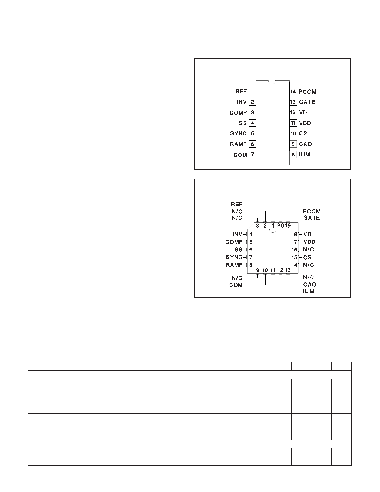
CONNECTION DIAGRAMS
DIL-14, SOIC-14 (Top View)
J, N, or D Packages
PLCC-20 (Top View)
Q Package
ELECTRICAL CHARACTERISTICS: Unless otherwise stated, these specifications apply for T
= –55°C to 125°C for
A
UCC1583, –40°C to 85°C for UCC2583, and 0°C to 70°C for UCC3583; VDD = 12V, RT= 60k, CT= 200pF, TA= TJ.
PARAMETER TEST CONDITIONS MIN TYP MAX UNITS
Ramp Generation and Synchronization
Maximum Input Operating Frequency For input with 5% to 90% duty cycle (Note 1) 500 kHz
Ramp Frequency, Free Running 95 100 105 kHz
Ramp Discharge Current V
= 0.5V 2.0 3.6 mA
RAMP
Low Threshold Voltage No min, no max, 0=TYP 0 V
High Threshold Voltage 3.75 4 4.25 V
Synchronizing Threshold Voltage (On) (Note 1) 1 V
Synchronizing Comparator Hysteresis 1 V
Output Duty Cycle
Minimum Duty Cycle Output D/C = Output PW / Input PW 0 %
Maximum Duty Cycle Output D/C = Output PW / Input PW 100 %
2

UCC1583
UCC2583
UCC3583
ELECTRICAL CHARACTERISTICS:
Unless otherwise stated, these specifications apply for TA= –55°C to 125°C for
UCC1583, –40°C to 85°C for UCC2583, and 0°C to 70°C for UCC3583; VDD = 12V, RT= 60k, CT= 200pF, TA= TJ.
PARAMETER TEST CONDITIONS MIN TYP MAX UNITS
Voltage Error Amplifier
V
V
INV
I
INV
Low V
V
COMP
V
High V
COMP
= VINV, 0°C to 70°C (UCC3583) 2.462 2.5 2.538 V
COMP
V
= VINV, All Other Temperature Ranges 2.45 2.5 2.55 V
COMP
V
= VINV 300 500 nA
COMP
= 2.6V, ICOMP = 100µA 450 700 mV
INV
= 2.4V, ICOMP = –100µA 5.0 5.5 6.0 V
INV
AVOL No Load 70 90 dB
GBW Product At f = 100kHz, T
A = 25°C (Note 1) 3 5 MHz
Current Error Amplifier
Input Offset Voltage 10 mV
Input CM Low Common Mode for CS and ILIM (Note 1) 0 V
Input CM High Common Mode for CS and ILIM (Note 1) 2 V
Low V
V
CAO
V
High V
CAO
+IN
+IN
= 0V, V
= 0V, V
= 0.1V, ICAO = 100µA 250 500 mV
–IN
= 0.1V, ICAO = –100µA 5.0 5.5 6.0 V
–IN
Input Current (ILIM and CS Pins) –50 0 50 nA
AVOL No Load 70 90 dB
GBW Product At f = 100kHz, T
= 25°C 2 4 MHz
A
Soft Start Current 10 25 µA
UVLO
VDD On Threshold Voltage 8.5 9.0 9.5 V
VDD Off Threshold Voltage 7.9 8.4 8.9 V
UVLO Hysteresis 0.3 0.6 0.9 V
Bias Supply
Supply Clamp Voltage 13 14 15 V
Supply Current (VDD) f = 100kHz With No Gate Output Load 3 5 mA
Output Driver
SAT High I
V
= –150mA 0.6 1.0 V
GATE
VSAT Low IGATE = 50mA 0.4 0.75 V
Rise Time C
GATE = 1nF 50 75 ns
Fall Time CGATE = 330pF 20 40 ns
Reference
VREF IREF = 0, 0°C to 70°C (UCC3583) 4.925 5 5.075 V
REF = 0, All Other Temperature Ranges 4.900 5 5.100 V
I
Line Regulation VDD = 10V to 14V 2 30 mV
Load Regulation IREF = 0mA to 2mA 1 20 mV
Note 1: Guaranteed by design. Not 100% tested in production.
3
 Loading...