

查询HPA00033DTR供应商
Single Ended Active Clamp/Reset PWM
UCC1580-1,-2,-3,-4
UCC2580-1,-2,-3,-4
UCC3580-1,-2,-3,-4
FEATURES
Provides Auxiliary Switch Activation
•
Complementary to Main Power
Switch Drive
Programmable deadtime (Turn-on
•
Delay) Between Activation of Each
Switch
Voltage Mode Control with
•
Feedforward Operation
Programmable Limits for Both
•
Transformer Volt- Second Product
and PWM Duty Cycle
High Current Gate Driver for Both
•
Main and Auxiliary Outputs
Multiple Protection Features with
•
Latched Shutdown and Soft Restart
• Low Supply Current (100µA Startup,
1.5mA Operation)
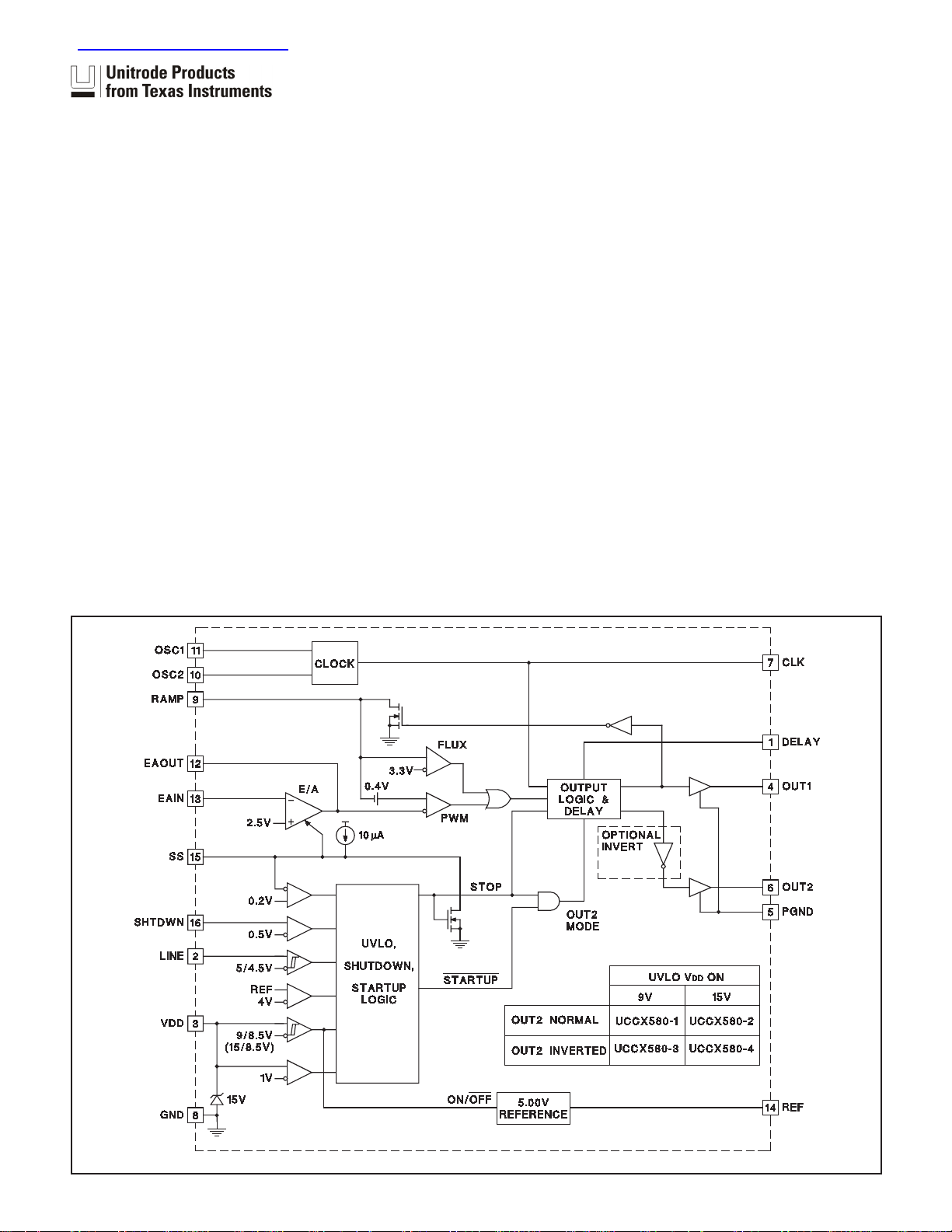
BLOCK DIAGRAM
DESCRIPTION
The UCC3580 family of PWM controllers is designed to implement a variety
of active clamp/reset and synchronous rectifier switching converter topolo
gies. While containing all the necessary functions for fixed frequency, high
performance pulse width modulation, the additional feature of this design is
the inclusion of an auxiliary switch driver which complements the main
power switch, and with a programmable deadtime or delay between each
transition. The active clamp/reset technique allows operation of single
ended converters beyond 50% duty cycle while reducing voltage stresses
on the switches, and allows a greater flux swing for the power transformer.
This approach also allows a reduction in switching losses by recovering en
ergy stored in parasitic elements such as leakage inductance and switch
capacitance.
The oscillator is programmed with two resistors and a capacitor to set
switching frequency and maximum duty cycle. A separate synchronized
ramp provides a voltage feedforward pulse width modulation and a pro
grammed maximum volt-second limit. The generated clock from the oscilla
tor contains both frequency and maximum duty cycle information.
(continued)
-
-
-
-
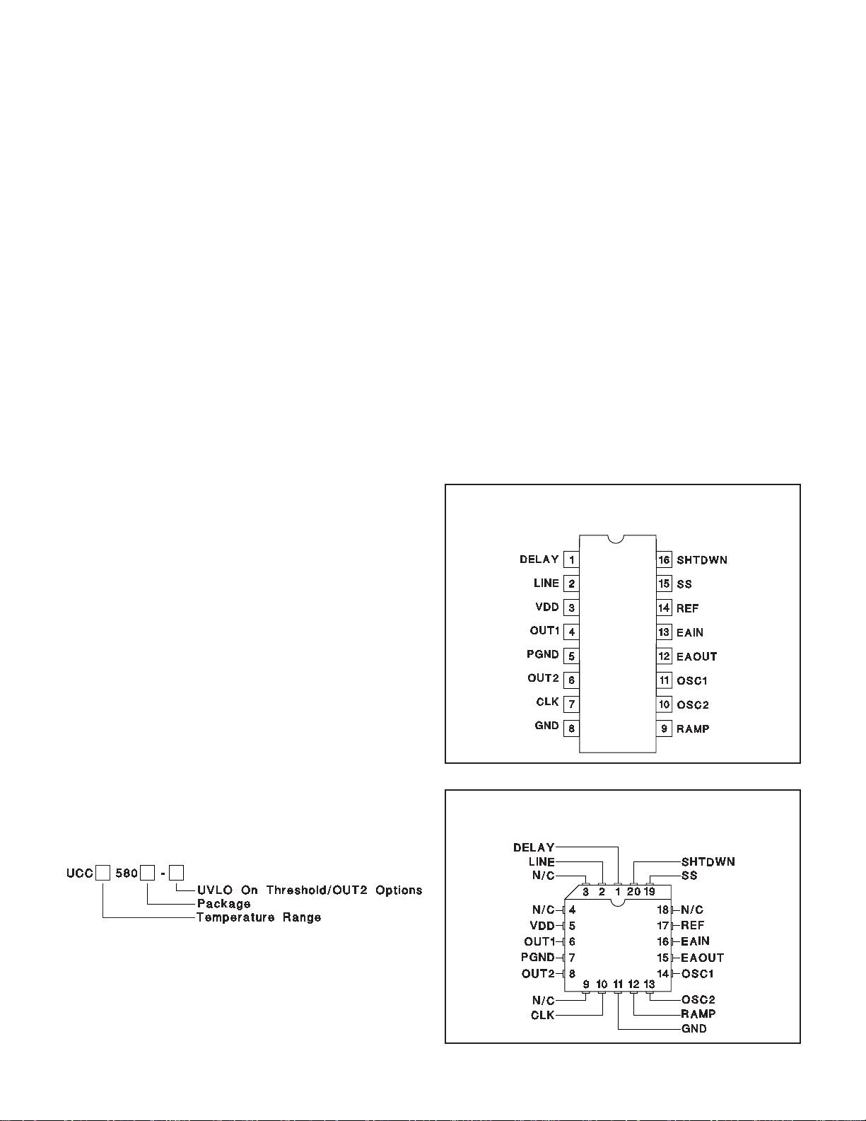
Pin Numbers refer to DIL-16 and SOIC-16 packages
SLUS292A - FEBRUARY 1999 - REVISED JANUARY 2002
UDG-95069-2
DESCRIPTION (cont.)
The main gate drive output (OUT1) is controlled by the
pulse width modulator. The second output (OUT2) is in
tended to activate an auxiliary switch during the off time
of the main switch, except that between each transition
there is deadtime where both switches are off, pro
grammed by a single external resistor. This design offers
two options for OUT2, normal and inverted. In the -1 and
-2 versions, OUT2 is normal and can be used to drive
PMOS FETs. In the -3 and -4 versions, OUT2 is inverted
and can be used to drive NMOS FETs. In all versions,
both the main and auxiliary switches are held off prior to
startup and when the PWM command goes to zero duty
cycle. During fault conditions, OUT1 is held off while
OUT2 operates at maximum duty cycle with a guaran
teed off time equal to the sum of the two deadtimes.
UCC1580-1,-2,-3,-4
UCC2580-1,-2,-3,-4
UCC3580-1,-2,-3,-4
Undervoltage lockout monitors supply voltage (VDD), the
-
precision reference (REF), input line voltage (LINE), and
the shutdown comparator (SHTDWN). If after any of
these four have sensed a fault condition, recovery to full
-
operation is initiated with a soft start. VDD thresholds, on
and off, are 15V and 8.5V for the -2 and -4 versions, 9V
and 8.5V for the -1 and -3 versions.
The UCC1580-x is specified for operation over the mili
tary temperature range of −55°C to 125°C. The
UCC2580-x is specified from −40°C to 85°C. The
UCC3580-x is specified from 0°C to 70°C. Package op
tions include 16-pin surface mount or dual in-line, and
20-pin plastic leadless chip carrier.
-
-
-
ABSOLUTE MAXIMUM RATINGS
VDD . . . . . . . . . . . . . . . . . . . . . . . . . . . . . . . . . . . . . . . . . . . 16V
I
. . . . . . . . . . . . . . . . . . . . . . . . . . . . . . . . . . . . . . . . . . 25mA
VDD
LINE, RAMP . . . . . . . . . . . . . . . . . . . . . . . . −0.3V to VDD + 1V
I
LINE,IRAMP
DELAY . . . . . . . . . . . . . . . . . . . . . . . . . . . . . . . . . . . . . . . . 5.3V
I
DELAY
I
OUT1
I
OUT2
I
. . . . . . . . . . . . . . . . . . . . . . . . . . . . . . . . −100mA to 100mA
CLK
OSC1, OSC2, SS, SHTDWN, EAIN . . . . . −0.3V to REF + 0.3V
I
EAOUT
I
. . . . . . . . . . . . . . . . . . . . . . . . . . . . . . . . . . . . . . . . . −30mA
REF
PGND. . . . . . . . . . . . . . . . . . . . . . . . . . . . . . . . . . −0.2V to 0.2V
Storage Temperature . . . . . . . . . . . . . . . . . . . −65°C to +150°C
Junction Temperature. . . . . . . . . . . . . . . . . . . −55°C to +150°C
Lead Temperature (Soldering, 10 sec.) . . . . . . . . . . . . . +300°C
All voltages are with respect to ground unless otherwise stated.
Currents are positive into, negative out of the specified termi
nal. Consult Packaging Section of Databook for thermal limita
tions and considerations of packages.
. . . . . . . . . . . . . . . . . . . . . . . . . . . . . . . . . . . . . 5mA
. . . . . . . . . . . . . . . . . . . . . . . . . . . . . . . . . . . . . . . . −5mA
(tpw < 1µs and Duty Cycle < 10%) . . . . . . . −0.6A to 1.2A
(tpw < 1µs and Duty Cycle < 10%) . . . . . . . −0.4A to 0.4A
. . . . . . . . . . . . . . . . . . . . . . . . . . . . . . . . . . −5mA to 5mA
ORDER INFORMATION
CONNECTION DIAGRAMS
DIL-16, SOIC-16 (Top View)
J, N, or D Packages
-
-
PLCC-20 (Top View)
Q Packages
2
UCC1580-1,-2,-3,-4
UCC2580-1,-2,-3,-4
UCC3580-1,-2,-3,-4
ELECTRICAL CHARACTERISTICS
= 12V, R1 = 18.2k, R2 = 4.41k, C
for the UCC2580, −55°C to 125°C for the UCC1580, T
= 100pF, R3 = 100k, C
T
Unless otherwise stated, all specifications are over the full temperature range, VDD
OUT1
A=TJ
= 0, C
.
= 0. TA= 0°C to 70°C for the UCC3580, −40°C to 85°C
OUT2
PARAMETER TEST CONDITIONS MIN TYP MAX UNITS
Oscillator Section
Frequency 370 400 430 kHz
CLK Pulse Width 650 750 850 ns
I
CLK V
CLK V
OH
OL
= −3mA 4.3 4.7 V
CLK
I
= 3mA 0.3 0.5 V
CLK
Ramp Generator Section
I
Ramp V
OL
= 100µA 50 100 mV
RAMP
Flux Comparator Vth 3.16 3.33 3.50 V
Pulse Width Modulator Section
Minimum Duty Cycle OUT1, EAOUT = VOL 0 %
Maximum Duty Cycle OUT1, EAIN = 2.6V 63 66 69 %
PWM Comparator Offset 0.1 0.4 0.9 V
Error Amplifier Section
EAIN EAOUT = EAIN 2.44 2.5 2.56 V
I
EAIN
EAOUT, VOL EAIN = 2.6V, I
EAOUT, VOH EAIN = 2.4V, I
EAOUT = EAIN 150 400 nA
= 100µA 0.3 0.5 V
EAOUT
= −100µA 4 5 5.5 V
EAOUT
AVOL 70 80 dB
Gain Bandwidth Product f = 100kHz (Note 1) 2 6 MHz
Softstart/Shutdown Section
Start Duty Cycle EAIN = 2.4V 0 %
OL I
SS V
= 100µA 100 350 mV
SS
SS Restart Threshold 400 550 mV
I
SS
SHTDWN V
I
SHTDWN
TH
0.4 0.5 0.6 V
–20 –35 µA
50 150 nA
Undervoltage Lockout Section
VDD On UCC3580-2,-4 14 15 16 V
UCC3580-1,-3 8 9 10 V
VDD Off 7.5 8.5 9.5 V
LINE On 4.7 5 5.3 V
LINE Off 4.2 4.5 4.8 V
I
LINE
LINE = 6V 50 150 nA
Supply Section
VDD Clamp I
I
Start VDD < VDD On 160 250 µA
VDD
I
Operating No Load 2.5 3.5 mA
VDD
= 10mA 14 15 16 V
VDD
Output Drivers Section
OUT1 V
OUT1 V
OUT2 V
OUT2 V
High I
SAT
Low I
SAT
High I
SAT
Low I
SAT
OUT1 Fall Time C
OUT1 Rise Time C
OUT2 Fall Time C
= −50mA 0.4 1.0 V
OUT1
=100mA 0.4 1.0 V
OUT1
= −30mA 0.4 1.0 V
OUT2
= 30mA 0.4 1.0 V
OUT2
= 1nF, RS = 3Ω 20 50 ns
OUT1
= 1nF, RS = 3Ω 40 80 ns
OUT1
= 300pF, RS = 10Ω 20 50 ns
OUT2
3
UCC1580-1,-2,-3,-4
UCC2580-1,-2,-3,-4
UCC3580-1,-2,-3,-4
ELECTRICAL CHARACTERISTICS
= 12V, R1 = 18.2k, R2 = 4.41k, C
for the UCC2580, −55°C to 125°C for the UCC1580, T
PARAMETER TEST CONDITIONS MIN TYP MAX UNITS
Output Drivers Section (cont.)
OUT2 Rise Time C
Delay 1 OUT2 to OUT1 R3 = 100k, C
Delay 2 OUT1 to OUT2 R3 = 100k, C
Reference Section
REF I
Load Regulation I
Line Regulation VDD = 10V to 14V 1 20 mV
Note 1: Guaranteed by design. Not 100% tested in production.
= 100pF, R3 = 100k, C
T
Unless otherwise stated, all specifications are over the full temperature range, VDD
= 0, C
OUT1
.
A=TJ
= 300pF, RS= 10Ω 20 40 ns
OUT2
OUT1
T
T
= 25°C 100 120 140 ns
A=TJ
OUT1
= 25°C 140 170 200 ns
A=TJ
= 0 4.875 5 5.125 V
REF
= 0mA to 1mA 1 20 mV
REF
= 0. TA= 0°C to 70°C for the UCC3580, −40°C to 85°C
OUT2
= C
= C
= 15pF 90 120 160 ns
OUT2
= 15pF 110 170 250 ns
OUT2
PIN DESCRIPTIONS
CLK: Oscillator clock output pin from a low impedance
CMOS driver. CLK is high during guaranteed off time.
CLK can be used to synchronized up to five other
UCC3580 PWMs.
DELAY: A resistor from DELAY to GND programs the
nonoverlap delay between OUT1 and OUT2. The delay
times, Delay1 and Delay2, are shown in Figure 1 and are
as follows:
Delay pF R
111 3=•.
Delay2 is designed to be larger than Delay1 by a ratio
shown in Figure 2.
EAIN: Inverting input to the error amplifier. The
noninverting input of the error amplifier is internally set to
2.5V. EAIN is used for feedback and loop compensation.
EAOUT: Output of the error amplifier and input to the
PWM comparator. Loop compensation components
connect from EAOUT to EAIN.
GND: Signal Ground.
LINE: Hysteretic comparator input. Thresholds are 5.0V
and 4.5V. Used to sense input line voltage and turn off
OUT1 when the line is low.
OSC1 & OSC2: Oscillator programming pins. A resistor
connects each pin to a timing capacitor. The resistor
connected to OSC1 sets maximum on time. The resistor
connected to OSC2 controls guaranteed off time. The
combined total sets frequency with the timing capacitor.
Frequency and maximum duty cycle are approximately
given by:
Frequency
=
()
R1 1.25 R2 CT
1
+••
Maximum Duty Cycle
=
Maximum Duty Cycle for OUT1 will be slightly less due to
Delay1 which is programmed by R3.
OUT1: Gate drive output for the main switch capable of
sourcing up to 0.5A and sinking 1A.
OUT2: Gate drive output for the auxiliary switch with
± 0.3A drive current capability.
PGND: Ground connection for the gate drivers. Connect
PGND to GND at a single point so that no high frequency
components of the output switching currents are in the
ground plane on the circuit board.
RAMP: A resistor (R4) from RAMP to the input voltage
and a capacitor (CR) from RAMP to GND programs the
feedforward ramp signal. RAMP is discharged to GND
when CLK is high and allowed to charge when CLK is
low. RAMP is the line feedforward sawtooth signal for the
PWM comparator. Assuming the input voltage is much
greater than 3.3V, the ramp is very linear. A flux
comparator compares the ramp signal to 3.3V to limit the
maximum allowable volt-second product:
Volt-Second Product Clamp = 3.3 • R4 • CR.
REF: Precision 5.0V reference pin. REF can supply up to
5mA to external circuits. REF is off until VDD exceeds 9V
(–1 and –3 versions) or activates the 15V clamp (–2 and
–4 versions) and turns off again when VDD droops below
8.5V. Bypass REF to GND with a 1µF capacitor.
SHTDWN: Comparator input to stop the chip. The
threshold is 0.5V. When the chip is stopped, OUT1 is low
and OUT2 continues to oscillate with guaranteed off time
equal to two non-overlap delay times.
4
R1
R1 1.25 R2
+•
 Loading...