

Page 1
9-Line Low Capacitance SCSI Active Terminator
FEATURES DESCRIPTION
• Complies with SCSI, SCSI-2
Standards
• 9pF Channel Capacitance during
Disconnect
• 100µA Supply Current in
Disconnect Mode
• Meets SCSI Hot Plugging Capability
•−300mA Sourcing Current for
Termination
• +40mA Sinking Current for Active
Negation
• Logic Command Disconnects all
Termination Lines
• Trimmed Termination Current to 7%
• Trimmed Impedance to 7%
• Current Limit and Thermal
Shutdown Protection
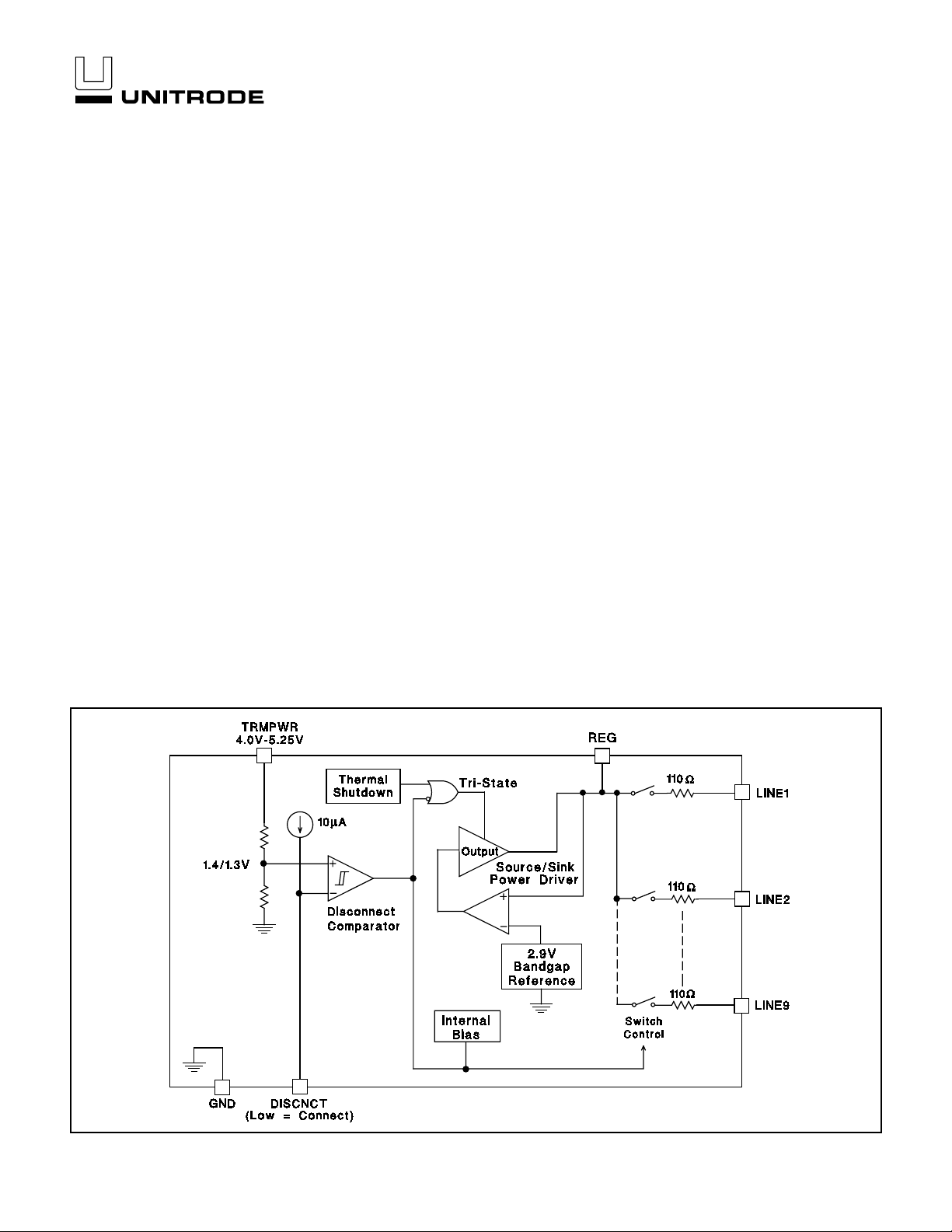
The UC5604 provides 9 lines of active termination for a SCSI (Small Computer Systems Interface) parallel bus. The SCSI standard recommends active termination at both ends of the cable segment.
The UC5604 provides a disconnect feature which, when opened or driven
high, will disconnect all terminating resistors and disable the regulator,
greatly redu cing stan dby power. The output c hannels remain high impedance even without Termpwr applied.
The UC5604 is pin-for-pin compatibl e with its predeces sor, the UC5603 - 9
line Active Terminator. The only functiona l di fference be tw een the UC5604
and UC5603 is the absence of the negative clamps. Parametrically, the
UC5604 has a 7 % tol er ance o n im peda nce and current compared to a 3%
tolerance on the UC5603 and the sink current is reduced from 300mA to
40mA. Custom power packages are utilized to allow normal operation at
full power conditions (1.2 watts).
Internal circuit trimming is utilized, first to trim the impedance to a 7% tolerance, and the n most importantly, to trim the output current to a 7% tolerance, as close to the max SCSI spec as possible, which maximiz es noise
margin in fast SCSI operation.
Other features include thermal shutdown and current limit.
This device is offered in low thermal resistance versions of the industry
standard 16 pin narrow body SO IC, 16 pin ZIP (zig-zag in line package)
and 24 pin TSSOP.
UC5604
BLOCK DIAGRAM
3/97
UDG-94064
Circuit Design Patented
Page 2
ABSOLUTE MAXIMUM RATINGS
Termpwr V o ltage . . . . . . . . . . . . . . . . . . . . . . . . . . . . . . . . . . . . . . . . . . . . . . . . . . . +7V
Signal Line Voltage. . . . . . . . . . . . . . . . . . . . . . . . . . . . . . . . . . . . . . . . . . . . . 0V to +7V
Regulator Output Current . . . . . . . . . . . . . . . . . . . . . . . . . . . . . . . . . . . . . . . . . . . . 0.5A
Storage Temperature . . . . . . . . . . . . . . . . . . . . . . . . . . . . . . . . . . . . . −65°C to +150°C
Operating Temperature . . . . . . . . . . . . . . . . . . . . . . . . . . . . . . . . . . . −55°C to +150°C
Lead Temperature (Soldering, 10 Sec.) . . . . . . . . . . . . . . . . . . . . . . . . . . . . . . . +300°C
Unless otherwise specified all voltages are with respe ct to G r ou nd . C urre nt s are pos itive into, negative out of the specified terminal.
Consult Packaging Section of Unitrode Integrated Circuits databook for thermal limitations and consid era ti ons of packages.
RECOMMENDED OPERATING CONDITIONS
Termpwr Voltage . . . . . . . . . . . . . . . . . . . . . . . . . . . . . . . . . . . . . . . . . . . 3.8V to 5.25V
Signal Line Voltage. . . . . . . . . . . . . . . . . . . . . . . . . . . . . . . . . . . . . . . . . . . . . 0V to +5V
Disconnect Input Voltage . . . . . . . . . . . . . . . . . . . . . . . . . . . . . . . . . . . . 0V to Termpwr
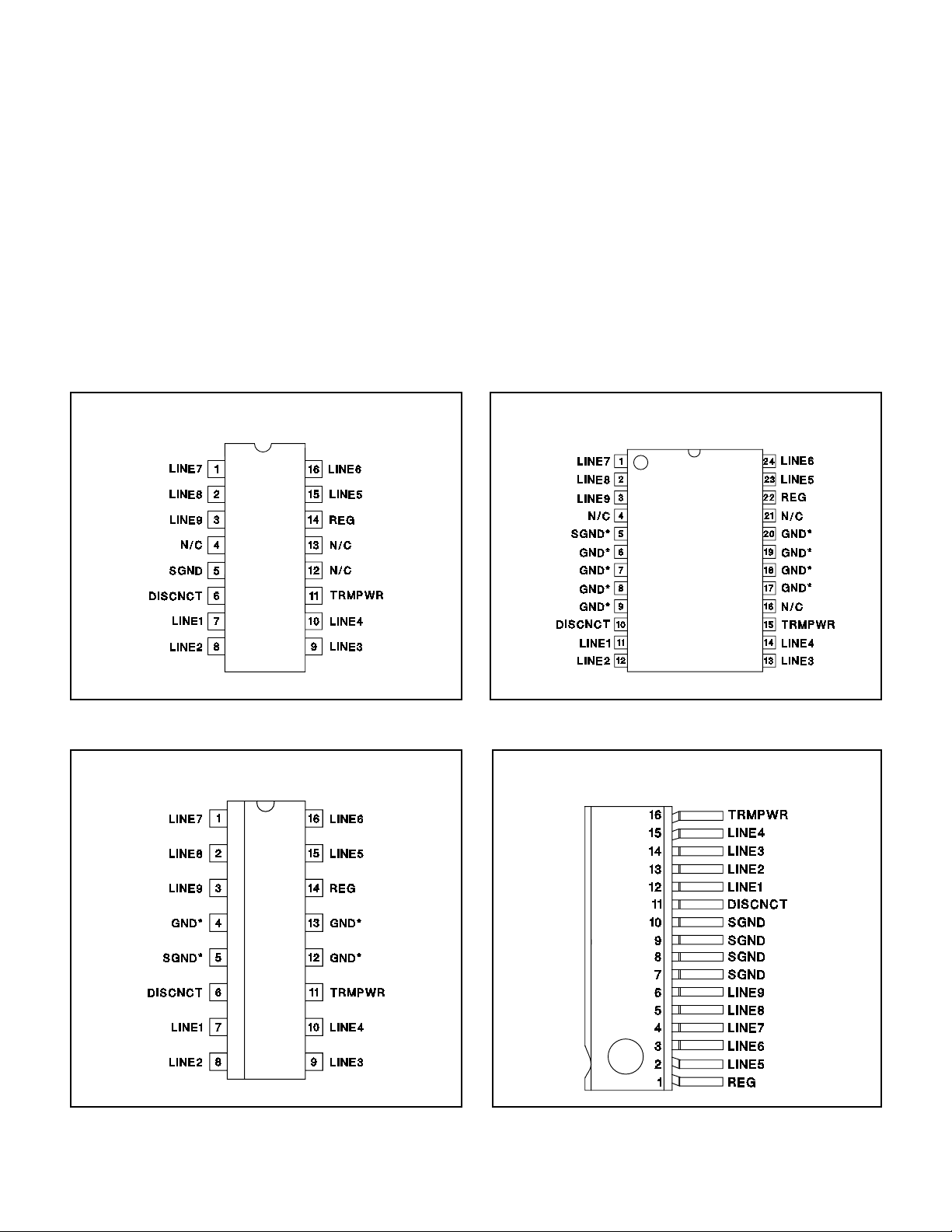
CONNECTION DIAGRAMS
DIL-16 (Top View)
N or J Package
TSSOP-24 (Top View)
PWP Package
UC5604
SOIC-16 (Top View)
DP Package
* DP packag e pi n 5 serves as signal groun d; pin s 4, 12, 13
serve as heatsink/ground.
* PWP pack ag e pi n 5 se rve s as sig na l gro un d; pins 6, 7, 8, 9,
17, 18, 19, and 20 serve as heatsink/ground.
ZIP-16 (Top View)
Z Package
Note: Drawings are not to scale.
2
Page 3

UC5604
ELECTRICAL CHARACTERISTICS
Unless otherwis e stat ed, th ese sp ecif icat io ns app ly for TA = 0°C to 70°C.
TRMPWR = 4.75V, DISCNCT = 0V. TA = TJ.
PARAMETER TEST CONDITIONS MIN TYP MAX UNITS
Supply Current Section
Termpwr Supply Current All termination lines = Open 14 20 mA
All termination li ne s = 0. 5V 200 220 mA
Power Down Mode DISCNCT = Open 100 150 µA
Output Section (Termina tor Lines)
Terminator Impedance ∆I
Output High Voltage TRMPWR = 4V (Note 1) 0°C < T
Max Output Cu rr e nt V
Max Output Cu rr e nt V
Output Clamp Level I
Output Leakag e
= -5mA to -15mA 97 110 129 Ohms
LINE
< 70°C2.55 3.2 V
J
= 25°C 2.6 2.9 3.1 V
T
J
= 0.5V TJ = 25°C -19.5 -21.9 -22.4 mA
LINE
0°C < T
= 0.5V, TRMPWR = 4V (Note 1) TJ = 25°C -18.0 -21.9 -22.4 mA
LINE
0°C < T
= -30mA -0.2 -0.05 0.1 V
LINE
DISCNCT = 4V
TRMPWR = 0V to 5.25V
REG = 0V
V
V
TRMPWR = 0V to 5.25V, REG = Open
= 0V to 5.25V
V
LINE
< 70°C -18.5 -21.9 -22.4 mA
J
< 70°C -17.0 -21.9 -22.4 mA
J
= 0 to 4V 10 400 nA
LINE
= 5.25V 100 µA
LINE
10 400 nA
Output Capacitance DISCNCT = Open (Note 2) 9 12 pF
Regulator Section
Regulator Output Voltage 2.5 2.9 3.2 V
Regulator Outpu t Vol ta ge All Termination Li ne s = 5V 2.55 2.9 3.1 V
Line Regulation TRMPWR = 4V to 6V 10 20 mV
Load Regulation I
= +100mA to -100mA 20 50 mV
REG
Drop Out Voltage All Termination Lines = 0.5V 1.0 1.2 V
Short Circuit Current V
Sinking Current Capability V
= 0V -200 -400 -600 mA
REG
= 3.5V 20 40 mA
REG
Thermal Shutdown 170 °C
Thermal Shutdown Hysteresis 10 °C
Disconnect Section
Disconnect Threshold 1.1 1.4 1.7 V
Threshold Hysteresis 100 mV
Input Current DISCNCT = 0V 150 200 µA
Note 1: Measuring each terminatio n li ne wh il e ot he r 8 are lo w (0.5 V).
Note 2: Guaranteed by design. Not 10 0% tes te d in prod uc ti on.
APPLICATION INFORMATION
Figure 1: Typical SCSI Bus Configurations Utilizing 2 UC5604 Devices
UDG-94065
3
Page 4

APPLICATION INFORMATION (cont.)
Figure 2: Typical Wide SCSI Bus Configurations Util iz in g 3 UC56 04 Devi ce s.
UC5604
UDG-94066
UNITRODE CORPORATI ON
7 CONTINENTAL BLVD. • MERRIMACK, NH 03054
TEL. (603) 424- 24 10 • FAX (603) 424-3460
4
Page 5

PACKAGE OPTION ADDENDUM
www.ti.com
30-Mar-2005
PACKAGING INFORMATION
Orderable Device Status
(1)
Package
Type
Package
Drawing
Pins Package
Qty
Eco Plan
UC5604DP OBSOLETE SOIC D 16 TBD Call TI Call TI
UC5604DPTR OBSOLETE SOIC D 16 TBD Call TI Call TI
UC5604J OBSOLETE UTR 16 TBD Call TI Call TI
UC5604N OBSOLETE PDIP N 16 TBD Call TI Call TI
UC5604QP OBSOLETE PLCC FN 28 TBD Call TI CallTI
UC5604QPTR OBSOLETE PLCC FN 28 TBD Call TI CallTI
UC5604Z OBSOLETE UTR 16 TBD Call TI Call TI
(1)
The marketing status values are defined as follows:
ACTIVE: Product device recommended for new designs.
LIFEBUY: TI has announced that the device will be discontinued, and a lifetime-buy period is in effect.
NRND: Not recommended for new designs. Device is in production to support existing customers, but TI does not recommend using this part in
a new design.
PREVIEW: Device has been announced but is not in production. Samples may or may not be available.
OBSOLETE: TI has discontinued the production of the device.
(2)
Eco Plan - The planned eco-friendly classification: Pb-Free (RoHS) or Green (RoHS & no Sb/Br) - please check
http://www.ti.com/productcontent for the latest availability information and additional product content details.
TBD: The Pb-Free/Green conversion plan has not been defined.
Pb-Free (RoHS): TI's terms "Lead-Free" or "Pb-Free" mean semiconductor products that are compatible with the current RoHS requirements
for all 6 substances, including the requirement that lead not exceed 0.1% by weight in homogeneous materials. Where designed to be soldered
at high temperatures, TI Pb-Free products are suitable for use in specified lead-free processes.
Green (RoHS & no Sb/Br): TI defines "Green" to mean Pb-Free (RoHS compatible), and free of Bromine (Br) and Antimony (Sb) based flame
retardants (Br or Sb do not exceed 0.1% by weight in homogeneous material)
(2)
Lead/Ball Finish MSL Peak Temp
(3)
(3)
MSL, Peak Temp. -- The Moisture Sensitivity Level rating according to the JEDEC industry standard classifications, and peak solder
temperature.
Important Information and Disclaimer:The information provided on this page represents TI's knowledge and belief as of the date that it is
provided. TI bases its knowledge and belief on information provided by third parties, and makes no representation or warranty as to the
accuracy of such information. Efforts are underway to better integrate information from third parties. TI has taken and continues to take
reasonable steps to provide representative and accurate information but may not have conducted destructive testing or chemical analysis on
incoming materials and chemicals. TI and TI suppliers consider certain information to be proprietary, and thus CAS numbers and other limited
information may not be available for release.
In no event shall TI's liability arising out of such information exceed the total purchase price of the TI part(s) at issue in this document sold by TI
to Customer on an annual basis.
Addendum-Page 1
Page 6

IMPORTANT NOTICE
Texas Instruments Incorporated and its subsidiaries (TI) reserve the right to make corrections, modifications,
enhancements, improvements, and other changes to its products and services at any time and to discontinue
any product or service without notice. Customers should obtain the latest relevant information before placing
orders and should verify that such information is current and complete. All products are sold subject to TI’s terms
and conditions of sale supplied at the time of order acknowledgment.
TI warrants performance of its hardware products to the specifications applicable at the time of sale in
accordance with TI’s standard warranty. Testing and other quality control techniques are used to the extent TI
deems necessary to support this warranty . Except where mandated by government requirements, testing of all
parameters of each product is not necessarily performed.
TI assumes no liability for applications assistance or customer product design. Customers are responsible for
their products and applications using TI components. To minimize the risks associated with customer products
and applications, customers should provide adequate design and operating safeguards.
TI does not warrant or represent that any license, either express or implied, is granted under any TI patent right,
copyright, mask work right, or other TI intellectual property right relating to any combination, machine, or process
in which TI products or services are used. Information published by TI regarding third-party products or services
does not constitute a license from TI to use such products or services or a warranty or endorsement thereof.
Use of such information may require a license from a third party under the patents or other intellectual property
of the third party, or a license from TI under the patents or other intellectual property of TI.
Reproduction of information in TI data books or data sheets is permissible only if reproduction is without
alteration and is accompanied by all associated warranties, conditions, limitations, and notices. Reproduction
of this information with alteration is an unfair and deceptive business practice. TI is not responsible or liable for
such altered documentation.
Resale of TI products or services with statements different from or beyond the parameters stated by TI for that
product or service voids all express and any implied warranties for the associated TI product or service and
is an unfair and deceptive business practice. TI is not responsible or liable for any such statements.
Following are URLs where you can obtain information on other Texas Instruments products and application
solutions:
Products Applications
Amplifiers amplifier.ti.com Audio www.ti.com/audio
Data Converters dataconverter.ti.com Automotive www.ti.com/automotive
DSP dsp.ti.com Broadband www.ti.com/broadband
Interface interface.ti.com Digital Control www.ti.com/digitalcontrol
Logic logic.ti.com Military www.ti.com/military
Power Mgmt power.ti.com Optical Networking www.ti.com/opticalnetwork
Microcontrollers microcontroller.ti.com Security www.ti.com/security
Telephony www.ti.com/telephony
Video & Imaging www.ti.com/video
Wireless www.ti.com/wireless
Mailing Address: Texas Instruments
Post Office Box 655303 Dallas, Texas 75265
Copyright 2005, Texas Instruments Incorporated
 Loading...