

UC5602
SCSI Active Terminator
FEATURES DESCRIPTION
• Complies with SCSI, SCSI-2
Standards
• 10pF Channel Capacitance During
Disconnect
• Active Termination for 18 Lines
• Logic Command Disconnects all
Termination Lines
• Low Supply Current in Disconnect
Mode
• Trimmed Regulator for Accurate
Termination Current
• Current Limit and Thermal
Shutdown Protection
• 110 Ohm Termination
• Meets SCSI Hot Plugging
The UC5602 is a pi n compatible version of its predecessor, the UC5601,
and is targeted for high vol ume applicatio ns which req uire ac tive termination, but not the high performance of the UC5601. The major differences
are relaxed outpu t current and termination tolerances, and the absence of
low side clamps.
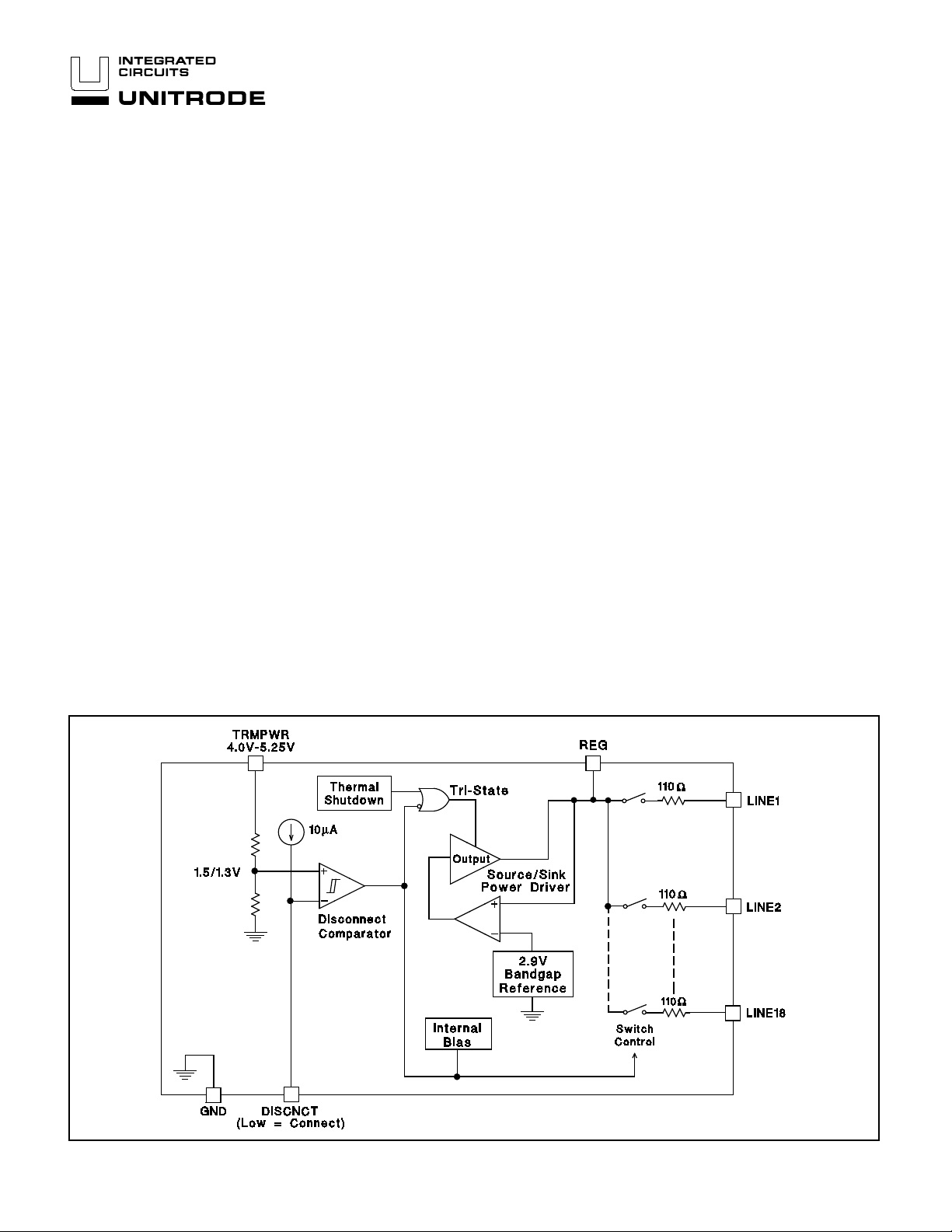
The UC5602 provides 18 lines of active termination for a SCSI (Small
Computer Systems Interface) paral lel bus. The SCSI-2 standard recommends active termination at both ends of the cable segment, and SCSI-3
will make it a requirement.
The UC5602 provides a disco nnect feature whi ch, when open ed or driven
high, will disconnect all termi nating resistors, and disables the regu lator;
greatly reduci ng standby powe r. The output channels remain high impedance even without Termpwr applied.
Internal circuit trimming is utilized, first to trim the impedance to a 7% tolerance; and then most importantly, to trim the output current 7% tolerance,
as close to the max SCSI as possible, which maximizes noise margin in
fast SCSI operation.
Other features include thermal shutdown, current limit, and 40mA of active
negation sink current capability.
BLOCK DIAGRAM
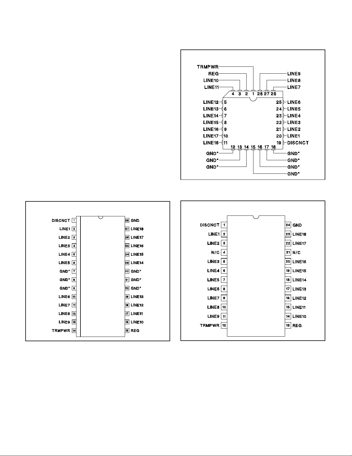
This device is offered in low thermal re sistance versions of the industry
standard 28 pin wide body SOIC and PLCC, as well as a 24 pin DIL plastic
package.
10/94
UDG-94052
Circuit Design Patented
UC5602
ABSOLUTE MAXIMUM RATINGS
Termpwr Voltage . . . . . . . . . . . . . . . . . . . . . . . . . . . . . . . . . +7V
Signal Line Voltage. . . . . . . . . . . . . . . . . . . . . . . . . . . 0V to +7V
Regulator Output Current. . . . . . . . . . . . . . . . . . . . . . . . . . 0.5A
Storage Temperature . . . . . . . . . . . . . . . . . . . −−65°C to +150°C
Operating Tem perat ure . . . . . . . . . . . . . . . . . −−55°C t o +150° C
Lead Temperat ure (Solde ring, 10 Sec.). . . . . . . . . . . . . +300°C
Unless otherwise specified all volta ges are with respect to
Ground. Cur ren ts are po sitive into, negative out of the specified terminal.
Consult Packaging Section of Unitr ode Int egr ated Circ uits databook for thermal limitations and consider ations of pack ages .
RECOMMENDED OPERATING CONDITIONS
Termpwr Voltage . . . . . . . . . . . . . . . . . . . . . . . . . 4.0V to 5.25V
Signal Line Voltage. . . . . . . . . . . . . . . . . . . . . . . . . . . 0V to +3V
Disconnect Input Voltage . . . . . . . . . . . . . . . . . . 0V to Termpwr
SOIC-28 (Top View)
DWP Package
CONNECTION DIAGRAMS
PLCC-28 (Top View)
QP Package
* QP package pins 12 - 18 serve as both hea tsink and sign al
ground.
DIL-24 (Top View)
N Package
* DWP package pin 28 serves as signal ground ; pins 7, 8, 9,
20, 21, 22 serve as heatsink/ground.
Note: Drawings are not to scale.
2
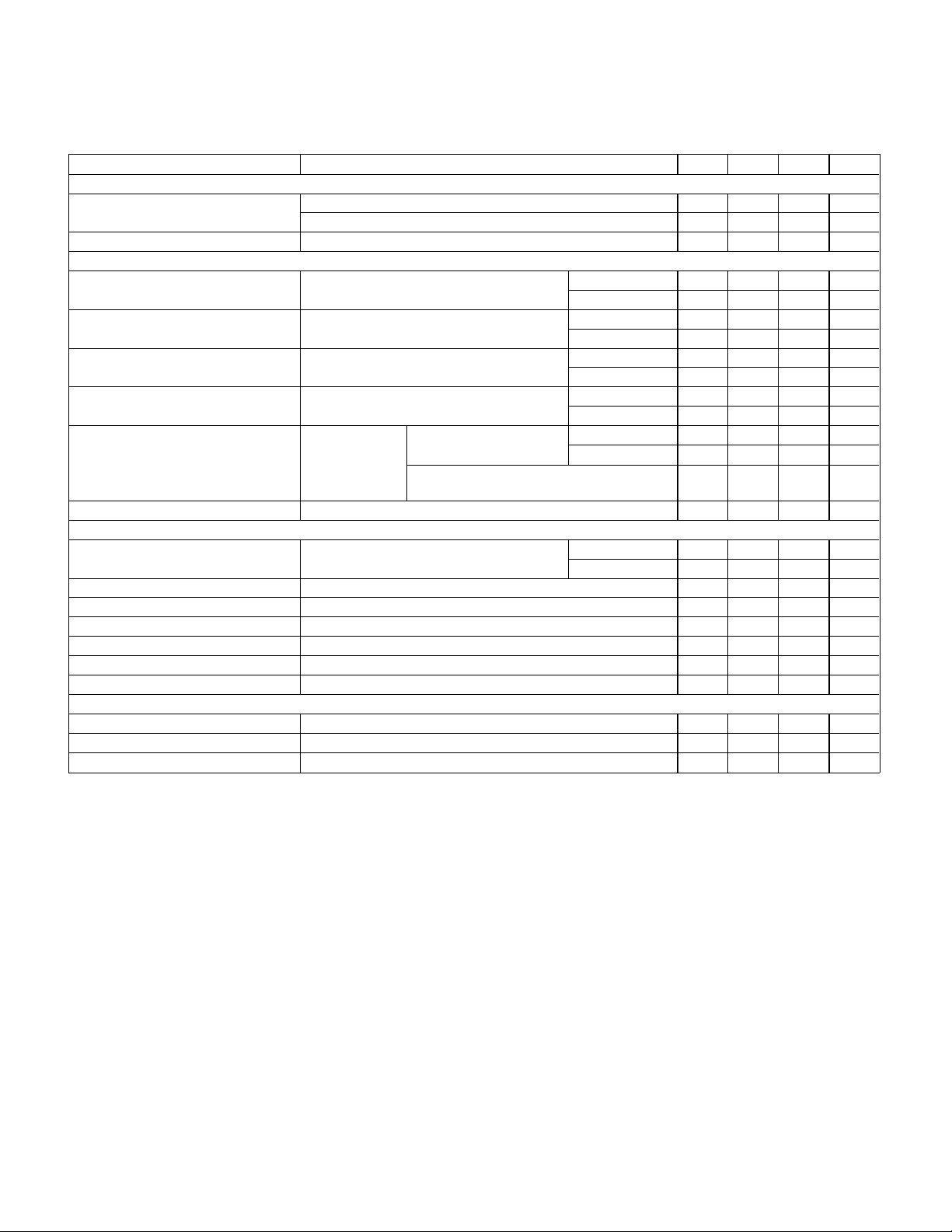
ELECTRICAL CHARACTERISTICS Unless otherwise stated, these specifications apply for TA = 0°C to 70°C.
TRMPWR = 4.75V, DISCNCT = 0V. T
PARAMETER TEST CONDITIONS MIN TYP MAX UNITS
Supply Cur rent Sect ion
Termpwr Supply Current All termination lines = Open 20 29 mA
Power Down Mode DISCNCT = Open 100 150 µA
Output Secti on (T erm inat i on Lines )
Termination Im peda nce ∆I
Output High Voltage V
Max Output Current V
Max Output Current V
Output Leakage
Output Capacit anc e DISCNCT = Open (Note 2) 10 13 pF
Regul ator Secti o n
Regulator Output Voltage T
Line Regulation TRMPWR = 4V to 6V 10 20 mV
Load Regulat io n I
Drop Out Voltage All Termination Lines = 0.5V 1.0 1.2 V
Short Circuit Cur rent V
Sinking Current Capabi lity V
Thermal Shutdow n 170 °C
Disconnect Section
Disconnect Threshold 1.1 1.4 1.7 V
Threshold Hys teres is 100 mV
Input Current DISCNCT = 0V 150 200 µA
Note 1: Measuring each term ination l ine while other 17 are low (0.5V).
Note 2: Guaranteed by design. Not 100% tested in production.
A = TJ.
All termination lines = 0.5V 400 435 mA
LINE = -5mA to -15mA TJ = 25°C 102 110 118 Ω
0°C < T
TRMPWR = 4V (Note 1) TJ = 25°C 2.6 2.9 3.1 V
0°C < T
LINE = 0.5V TJ = 25°C -19.5 -21.4 -22.4 mA
0°C < T
LINE = 0.5V, TRMPWR = 4V (Note 1) TJ = 25° C -18.0 -21.5 -22.4 mA
0°C < T
DISCNCT = 4V
TRMPWR = 0V to 5.25V
REG = 0V
V
V
TRMPWR = 0V to 5.25V, REG = Open
LINE = 0V to 5.25V
V
0°C < T
REG = 0 to -4 00mA 20 50 mV
REG = 0V -450 -650 -850 mA
REG = 3.5V 20 40 mA
J < 70°C 97 129 Ω
J < 70°C 2.55 3.2 V
J < 70°C -18.5 -22.4 mA
J < 70°C -17.0 -22.4 mA
LINE = 0 to 4V 10 400 nA
LINE = 5.25V 100 µA
10 400 nA
J = 25°C 2.7 2.9 3.1 V
J < 70°C 2.55 3.2 V
UC5602
THERMAL DATA
DWP package: (see packaging section of UICC data book for more details on thermal performance)
Thermal Resistance Junction to Leads, θjL . . . . . . . . . . . . . . . . . . . . . . . . . . . . . . . . . . . . . . . . . . . . . . 18°C/ W
Thermal Resistance Junction to Ambient, θja. . . . . . . . . . . . . . . . . . . . . . . . . . . . . . . . . . . . . . . . . . 33°-43°C/W
N package:
Thermal Resistance Junction to Leads, θjL . . . . . . . . . . . . . . . . . . . . . . . . . . . . . . . . . . . . . . . . . . . . . . 50°C/ W
Thermal Resistance Junction to Ambient, θja. . . . . . . . . . . . . . . . . . . . . . . . . . . . . . . . . . . . . . . . . 95°-105°C/W
QP package:
Thermal Resistance Junction to Leads, θjL . . . . . . . . . . . . . . . . . . . . . . . . . . . . . . . . . . . . . . . . . . . . . . 15°C/ W
Thermal Resistance Junction to Ambient, θja. . . . . . . . . . . . . . . . . . . . . . . . . . . . . . . . . . . . . . . . . . 30°-40°C/W
Note: The above n u mb ers for θjL are maximums for the limit ing ther ma l resistanc e of the packa ge in a standa rd mounting conf igu-
θ
ration. The
numbers assume no ambient airflow .
ja numbers are meant to be guidelines for the thermal per fo rmanc e of the device/pc -bo ard system . All of the abov e
3
 Loading...