

查询UC1824供应商
High Speed PWM Controller
FEATURES DESCRIPTION
• Complementary Outputs
• Practical Operation Switching Frequencies
to 1MHz
• 50ns Propagation Delay to Output
• High Current Dual Totem Pole Outputs
(1.5A Peak)
• Wide Bandwidth Error Amplifier
• Fully Latched Logic with Double Pulse
Suppression
• Pulse-by-Pulse Current Limiting
• Soft Start / Max. Duty Cycle Control
• Under-Voltage Lockout with Hysteresis
• Low Start Up Current (1.1 mA)
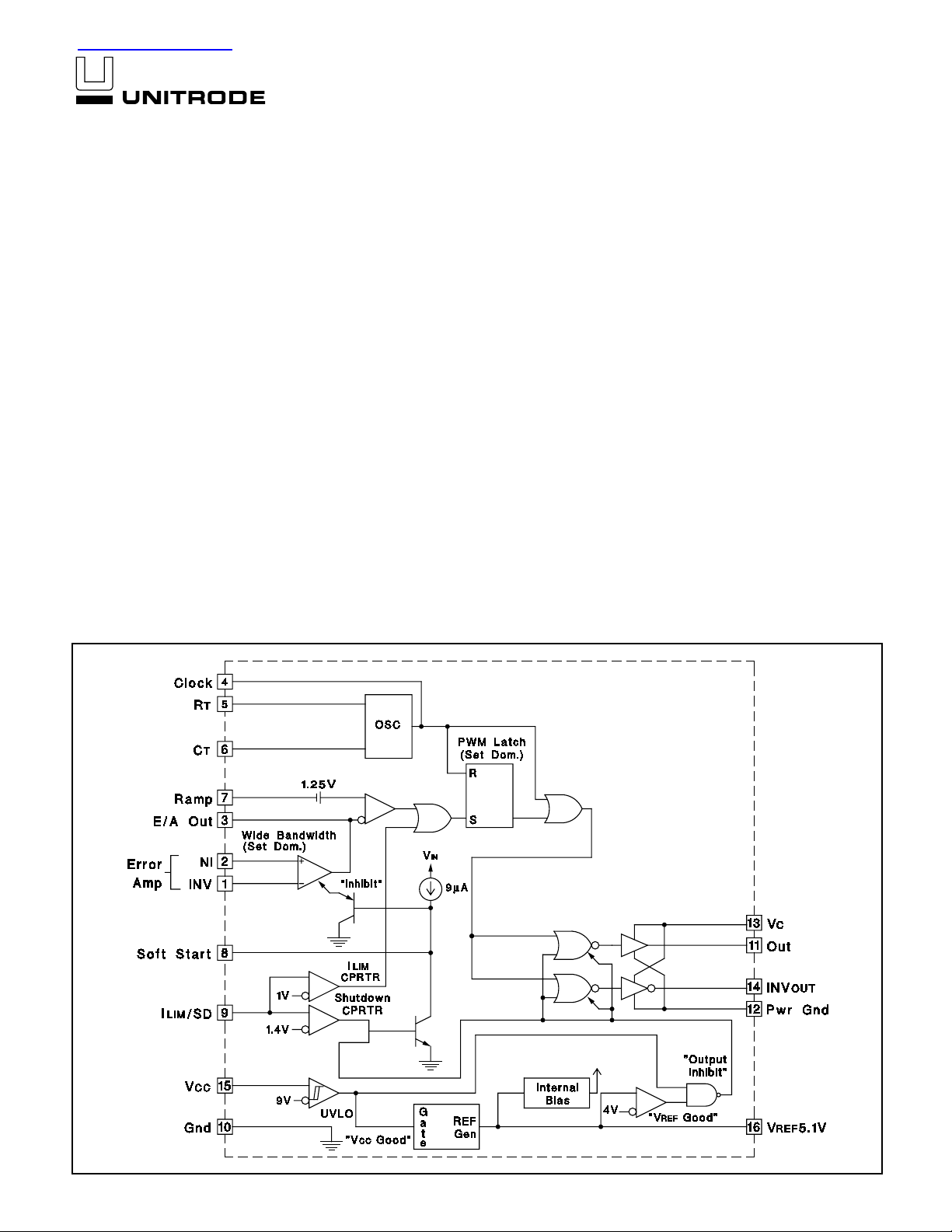
The UC1824 family of PWM control ICs is optimized for high frequency switched mode power supply applications. Particular care
was given to min imi zin g pr opagati on delays through the comparators
and logic c ircuitry while maximizing bandwidth and slew rate of the
error amplifier. This controller is designed for use in either currentmode or voltage mod e systems with the capability for input voltage
feed-forward.
Protection circuitry includes a current limit comparator with a 1V
threshold, a TTL compatible shutdown port, and a soft start pin which
will double as a maximum duty cycle clamp. The logic is fully latched
to provide jitter free operation and prohibit multiple pulses at an output. An under-voltage lockout s ection with 800mV of hysteresis assures low start up current. Dur ing under-voltage lockout, the outputs
are high impedance.
These devices feature totem pole outputs designed to source and
sink high peak currents from capacitive l oads, such as the gate of a
power MOSFET. The on state is designed as a high level.
UC1824
UC2824
UC3824
• Trimmed Bandgap Reference (5.1V ± 1%)
BLOCK DIAGRAM
3/97
UDG-92034-1
ABSOLUTE MAXIMUM RATINGS
(Note 1)
Supply Voltage (Pins 13, 15) . . . . . . . . . . . . . . . . . . . . . . . . 30V
Output Current, Source or Sink (Pins 11, 14)
DC. . . . . . . . . . . . . . . . . . . . . . . . . . . . . . . . . . . . . . . . . . . . 0.5A
Pulse (0.5µs) . . . . . . . . . . . . . . . . . . . . . . . . . . . . . . . . . . . 2.0A
Analog Inputs
(Pins 1, 2, 7) . . . . . . . . . . . . . . . . . . . . . . . . . . . . . . . -0.3V to 7V
(Pin 8, 9). . . . . . . . . . . . . . . . . . . . . . . . . . . . . . . . . . -0.3V to 6V
Clock Output Current (Pin 4) . . . . . . . . . . . . . . . . . . . . . . . -5mA
Error Amplifier Output Current (Pin 3) . . . . . . . . . . . . . . . . 5mA
Soft Start Sink Current (Pin 8) . . . . . . . . . . . . . . . . . . . . . 20mA
Oscillator Charging Current (Pin 5) . . . . . . . . . . . . . . . . . . -5mA
Power Dissipation . . . . . . . . . . . . . . . . . . . . . . . . . . . . . . . . 1W
Storage Temperature Range . . . . . . . . . . . . . . -65°C to +150°C
Lead Temperature (Soldering, 10 seconds) . . . . . . . . . . 300°C
Note 1: All voltages are with respect to GND (Pin 10); all currents are positive into, negative out of part; pin numbers refer to
DIL-16 package.
Note 3: Consult Unitrode Integrated Circuit Databook for thermal limitations and considerations of package.
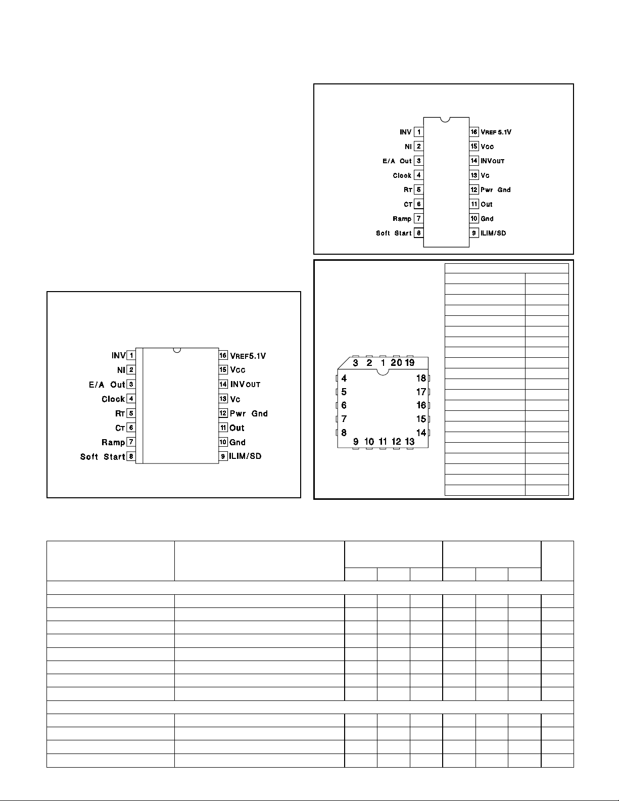
SOIC-16 (Top View)
DW Package
CONNECTION DIAGRAMS
DIL-16 (Top View)
J Or N Package
PLCC-20 & LCC-20
(Top View)
Q & L Packages
UC1824
UC2824
UC3824
PACKAGE PIN FUNCTION
FUNCTION
N/C 1
INV 2
NI 3
E/A Out 4
Clock 5
N/C 6
R
T
C
T
Ramp 9
Soft Start 10
N/C 11
ILIM/SD 12
Gnd 13
Out 14
Pwr Gnd 15
N/C 16
V
C
INV
OUT
V
CC
V
5.1V 20
REF
PIN
7
8
17
18
19
ELECTRICAL CHARACTERISTICS:
Unless otherwise stated,these spe ci fi ca tions apply for , RT = 3.65k, CT = 1nF, V
= 15V, -55°C<TA<125°C for the UC1824, –40°C<TA<85°C for the UC2824, and
0°C<TA<70°C for the UC3824, TA=T
PARAMETERS TEST CONDITIONS UC2824
J.
UC1824
UC3824
MIN TYP MAX MIN TYP MAX UNITS
Reference Section
Output Voltage T
Line Regulation 10V < V
Load Regulation 1mA < I
Temperature Stability* T
= 25°C, IO = 1mA 5.05 5.10 5.15 5.00 5.1 0 5.20 V
J
< 30V 2 20 2 20 mV
CC
< 10mA 5 20 5 20 mV
O
< TA < T
MIN
MAX
0.2 0.4 0.2 0.4 mV/°C
Total Output Variat io n* Li ne , Lo ad , Te mp era tu r e 5.00 5.20 4.95 5.25 V
Output Noise Volt ag e* 10Hz < f < 10kHz 50 50
= 125°C, 1000hrs. 5 25 5 25 mV
Long Term Stability* T
Short Circuit Current V
J
= 0V -15 -50 -100 -15 -50 -100 mA
REF
Oscillator Section
Initial Accuracy * TJ = 25°C 360 400 440 360 400 440 k Hz
< 30V 0.2 2 0.2 2 %
MIN
CC
< TA < T
MAX
55%
Voltage Stability* 10V < V
Temperature Stability* T
Total Variation* Line, Temperature 340 460 340 460 kHz
2
CC
µ
V
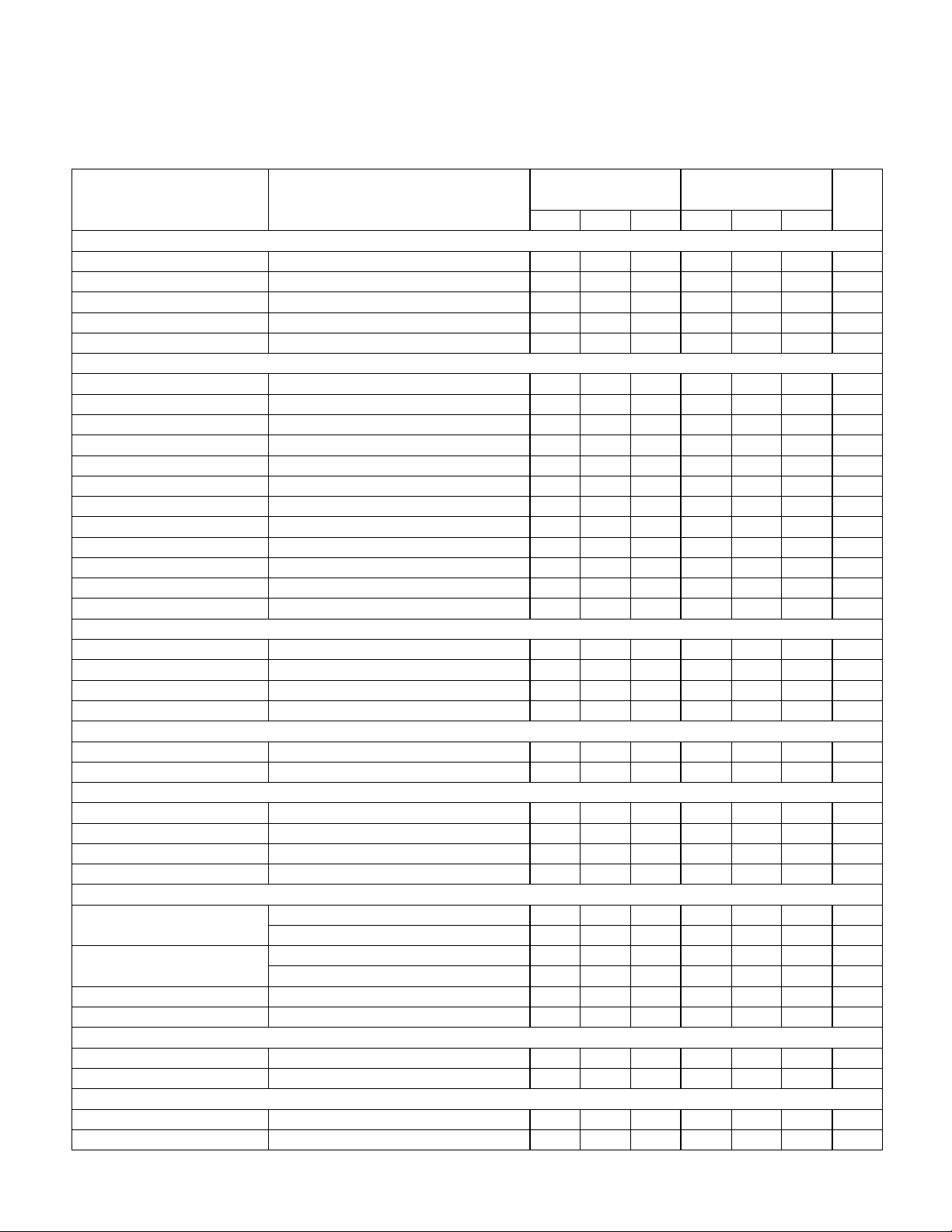
UC1824
UC2824
UC3824
ELECTRICAL CHARACTERISTICS
(cont.)
Unless otherwise stated,these spe ci fi ca tions apply for , R
= 1nF, VCC = 15V, -55°C<TA<125°C for the UC1824, –40°C<TA<85°C for the
UC2824, and 0°C<TA<70°C for the UC3824, TA=T
J.
UC1824
PARAMETERS TEST CONDITIONS UC2824
MIN TYP MAX MIN TYP MAX UNITS
Oscillator Section (cont. )
Clock Out High 3.9 4.5 3.9 4.5 V
Clock Out Low 2.3 2.9 2.3 2.9 V
Ramp Peak* 2.6 2.8 3.0 2.6 2.8 3.0 V
Ramp Valley* 0.7 1.0 1.25 0.7 1.0 1.25 V
Ramp Valley to Peak* 1.6 1.8 2.0 1.6 1.8 2.0 V
Error Amplifier Section
Input Offset Voltage 10 15 mV
Input Bias Current 0.6 3 0.6 3
Input Offset Current 0.1 1 0.1 1
Open Loop Gain 1V < V
CMRR 1.5V < V
PSRR 10V < V
Output Sink Current V
Output Source Current V
Output High Voltage I
Output Low Voltag e I
PIN 3
PIN 3
< 4V 60 95 60 95 dB
O
< 5.5V 75 95 75 95 dB
CM
< 30V 85 110 85 110 dB
CC
= 1V 12.5 12.5 mA
PIN 3
= 4V -0.5 -1.3 -0.5 -1.3 mA
PIN 3
= -0.5mA 4.0 4.7 5.0 4.0 4.7 5.0 V
= 1mA 0 0 .5 1.0 0 0.5 1.0 V
Unity Gain Bandwidth* 35.5 35.5 MHz
Slew Rate* 612 612 V/
PWM Comparator Section
Pin 7 Bias Current V
= 0V -1 -5 -1 -5
PIN 7
Duty Cycle Range 0 80 0 85 %
Pin 3 Zero DC Threshold V
= 0V 1.1 1.25 1.1 1.25 V
PIN 7
Delay to Output* 50 80 50 80 ns
Soft-Start Section
= 0.5V 3 9 20 3 9 20
Charge Current V
Discharge Current V
PIN 8
= 1V 1 1 mA
PIN 8
Current Limit / Shutdown Section
Pin 9 Bias Current 0 < V
< 4V 15 10
PIN 9
Current Limit Threshold 0.9 1.0 1.1 0.9 1.0 1.1 V
Shutdown Threshold 1.25 1.40 1.55 1.25 1.40 1.55 V
Delay to Output 50 80 50 80 ns
Output Section
= 20mA 0.25 0.40 0.25 0.40 V
Output Low Level I
Output High Level I
Collector Leakage V
OUT
I
= 200mA 1.2 2.2 1.2 2.2 V
OUT
= -20mA 13.0 13.5 13.0 13.5 V
OUT
I
= -200mA 12.0 13.0 12.0 13.0 V
OUT
= 30V 100 500 10 500
C
Rise/Fall Time* CL = 1nF 3060 3060ns
Under-Voltage Lockout Section
Start Threshold 8.8 9.2 9.6 8.8 9.2 9.6 V
UVLO Hysteresis 0.4 0.8 1.2 0.4 0.8 1.2 V
Supply Current Section
Start Up Current VCC = 8V 1.1 2.5 1.1 2.5 mA
ICC V
PIN 1
, V
PIN 7
, V
PIN 9
= 0V; V
= 1V 22 33 22 33 mA
PIN 2
* This parameter not 100% tested in production but guaranteed by design.
= 3.65k, C
T
UC3824
T
µ
µ
µ
µ
µ
µ
A
A
µ
s
A
A
A
A
3
 Loading...