

查询UC2710供应商
High Current FET Driver
UC1710
UC2710
UC3710
FEATURES
• Totem Pole Output with 6A
Source/Sink Drive
• 3ns Delay
• 20ns Rise and Fall Time into 2.2nF
• 8ns Rise and Fall Time into 30nF
• 4.7V to 18V Operation
• Inverting and Non-Inverting Outputs
• Under-Voltage Lockout with
Hysteresis
• Thermal Shutdown Protection
• MINIDIP and Power Packages
TRUTH TABLE
INV N.I. Out
HHL
LHH
HLL
LLL
OUT= INV and N.I.
OUT
= INV or N.I.
DESCRIPTION
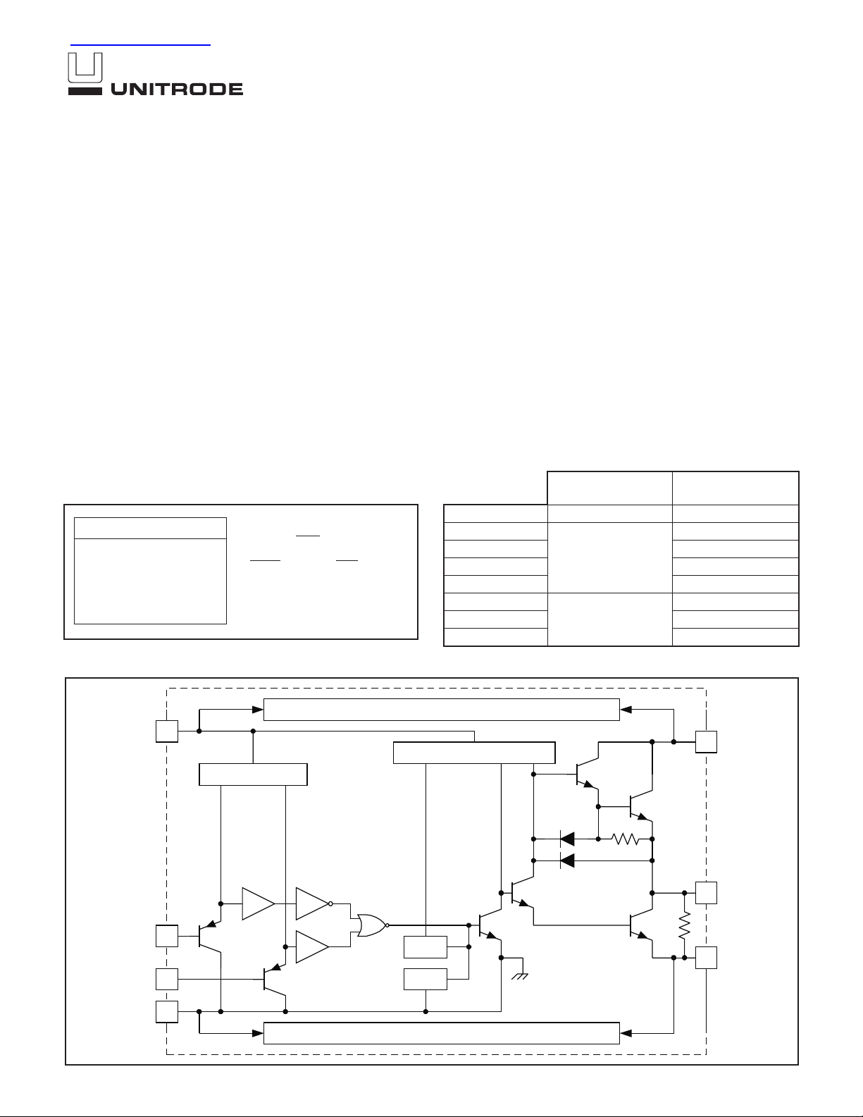
The UC1710 family of FET drivers is made with a high-speed Schottky process to interface between low-level control functions and very high-power
switching devices-particularly power MOSFET’s. These devices accept
low-current digital inputs to activate a high-current, totem pole output which
can source or sink a minimum of 6A.
Supply voltages for both V
and VCcan independently range from 4.7V to
IN
18V. These devices also feature under-voltage lockout with hysteresis.
The UC1710 is packaged in an 8-pin hermetically sealed dual in-line pack-
age for –55°C to +125°C operation. The UC2710 and UC3710 are specified for a temperature range of –40°C to +85°C and 0°C to +70°C
respectively and are available in either an 8-pin plastic dual in-line or a
5-pin, TO-220 package. Surface mount devices are also available.
ORDERING INFORMATION
TEMPERATURE
RANGE
UC1710J –55°C to +125°C 8 pin CDIP
UC2710DW –40°C to +85°C 16 pin SOIC-wide
UC2710J 8 pin CDIP
UC2710N 8 pin PDIP
UC2710T 5 pin TO220
UC3710DW 0°C to +70°C 16 pin SOIC-wide
UC3710N 8 pin PDIP
UC3710T 5 pin TO220
PACKAGE
BLOCK DIAGRAM
5
V
IN
N.I. IN
INV IN
Logic G nd
8
7
LOGIC BIAS
INTERNALLY CONNECTED IN T PACKAG E
OUTPUT BIAS
TSD
UVLO1
INTERNALLY CO NNECTED IN T PACKAGE
4
V
C
3
Out
2PwrGnd
UDG-99079
05/99
ABSOLUTE MAXIMUM RATINGS
N-Package J-Package T-Package
Supply Voltage, Vin . . . . . . . . . . . . . . . . . . . . . . . . . . . 20V . . . . . . . . . . . . . . 20V . . . . . . . . . . . . . . 20V
Collector Supply Voltage, VC. . . . . . . . . . . . . . . . . . . . 20V . . . . . . . . . . . . . . 20V . . . . . . . . . . . . . . 20V
Operating Voltage . . . . . . . . . . . . . . . . . . . . . . . . . . . . 18V . . . . . . . . . . . . . . 18V . . . . . . . . . . . . . . 18V
Output Current (Source or Sink)
Steady-State. . . . . . . . . . . . . . . . . . . . . . . . . . . . . ± 500mA. . . . . . . . . . . .±500mA . . . . . . . . . . . . . ± 1A
Digital Inputs. . . . . . . . . . . . . . . . . . . . . . . . . . . . –0.3V-VIN . . . . . . . . –0.3V – VIN. . . . . . . . –0.3V – VIN
Power Dissipation at Ta=25°C . . . . . . . . . . . . . . . . . . . 1W. . . . . . . . . . . . . . . 1W. . . . . . . . . . . . . . . 3W
Power Dissipation at T (Case) = 25°C. . . . . . . . . . . . . . 2W . . . . . . . . . . . . . . . 2W . . . . . . . . . . . . . . 25W
Operating Junction Temperature. . . . . . . –55°C to +150°C . . . . –55°C to +150°C . . . . –55°C to +150°C
Storage Temperature . . . . . . . . . . . . . . . –65°C to +150°C . . . . –65°C to +150°C . . . . –65°C to +150°C
Lead Temperature (Soldering, 10 seconds). . . . . . . 300°C . . . . . . . . . . . . 300°C . . . . . . . . . . . . 300°C
Note 1: All currents are positive into, negative out of the specified terminal.
Note 2: Consult Unitrode Integrated Circuits databook for information regarding thermal specifications
and limitations of packages.
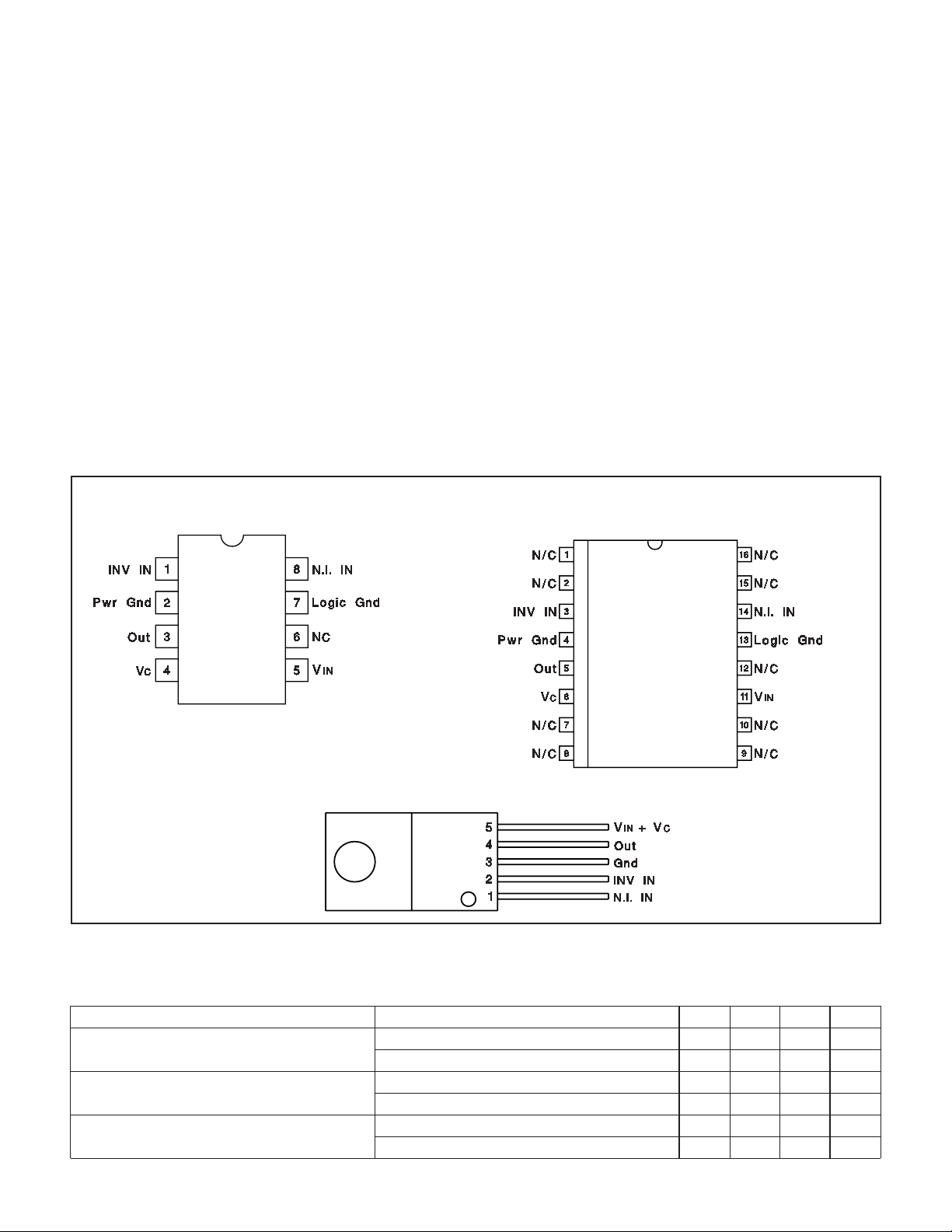
CONNECTION DIAGRAMS
UC1710
UC2710
UC3710
DIL-8 MINIDIP (Top View)
J or N Package
SOIC-16 (Top View)
DW Package
5-Pin TO-220 (Top View)
T Package
ELECTRICAL CHARACTERISTICS: Unless otherwise stated, these specifications apply for V
TA= T
J.
PARAMETERS TEST CONDITIONS MIN TYP MAX UNITS
VINSupply Current VIN=18V, VC=18V, Output Low 26 35 mA
VIN=18V, VC=18V, Output High 21 30 mA
V
Supply Current VIN=18V, VC=18V, Output Low 1.5 5.0 mA
C
VIN=18V, VC=18V,Output High 5.0 8 mA
UVLO Threshold VINHigh to Low 3.8 4.1 4.4 V
VINLow to High 4.1 4.4 4.8 V
= VC= 15V, No load,
IN
2

UC1710
UC2710
UC3710
ELECTRICAL CHARACTERISTICS:
TA= T
J.
Unless otherwise stated, these specifications apply for VIN= VC= 15V, No load,
PARAMETERS TEST CONDITIONS MIN TYP MAX UNITS
UVLO Threshold Hysteresis 0.1 0.3 0.5 V
Digital Input Low Level 0.8 V
Digital Input High Level 2.0 V
Digital Input Current Digital Input = 0.0V –70 –4.0 µA
Output High Sat., V
– V
C
O
IO= –100mA 1.35 2.2 V
IO= –6A 3.2 4.5 V
Output Low Sat., V
O
IO= 100mA 0.25 0.6 V
IO= 6A 3.4 4.5 V
Thermal Shutdown 165 °C
From Inv., Input to Output (Note 3, 4):
Rise Time Delay CL = 0 35 70 ns
CL = 2.2nF 35 70 ns
CL = 30nF 35 70 ns
10% to 90% Rise CL = 0 20 40 ns
CL = 2.2nF 25 40 ns
CL = 30nF 85 150 ns
Fall Time Delay CL = 0 35 70 ns
CL = 2.2nF 35 70 ns
CL = 30nF 35 80 ns
90% to 10% Fall CL = 0 15 40 ns
CL = 2.2nF 20 40 ns
CL = 30nF 85 150 ns
From N.I. Input to Output (Note 3,4):
Rise Time Delay CL = 0 35 70 ns
CL = 2.2nF 35 70 ns
CL = 30nF 35 70 ns
10% to 90% Rise CL = 0 20 40 ns
CL = 2.2nF 25 40 ns
CL = 30nF 85 150 ns
Fall Time Delay CL = 0 35 70 ns
CL = 2.2nF 35 70 ns
CL = 30nF 35 80 ns
90% to 10% Fall CL = 0 15 40 ns
CL = 2.2nF 20 50 ns
CL = 30nF 85 150 ns
Total Supply Current at 200kHz Input
T
= 25°C (Note 5) CL = 0 30 40 mA
A
Switching Frequency
Note: 3. Delay measured from 50% input change to 10% output change.
Note: 4. Those parameters with CL = 30nF are not tested in production.
Note: 5. Inv. Input pulsed at 50% duty cycle with N.I. Input = 3V. or N.I. Input pulsed at 50% duty cycle with Inv. Input = 0V.
UNITRODE CORPORATION
7 CONTINENTALBLVD. • MERRIMACK, NH 03054
TEL. (603) 424-2410 FAX (603) 424-3460
3

IMPORTANT NOTICE
T exas Instruments and its subsidiaries (TI) reserve the right to make changes to their products or to discontinue
any product or service without notice, and advise customers to obtain the latest version of relevant information
to verify, before placing orders, that information being relied on is current and complete. All products are sold
subject to the terms and conditions of sale supplied at the time of order acknowledgement, including those
pertaining to warranty, patent infringement, and limitation of liability.
TI warrants performance of its semiconductor products to the specifications applicable at the time of sale in
accordance with TI’s standard warranty. Testing and other quality control techniques are utilized to the extent
TI deems necessary to support this warranty . Specific testing of all parameters of each device is not necessarily
performed, except those mandated by government requirements.
CERTAIN APPLICATIONS USING SEMICONDUCTOR PRODUCTS MAY INVOLVE POTENTIAL RISKS OF
DEATH, PERSONAL INJURY, OR SEVERE PROPERTY OR ENVIRONMENTAL DAMAGE (“CRITICAL
APPLICATIONS”). TI SEMICONDUCTOR PRODUCTS ARE NOT DESIGNED, AUTHORIZED, OR
WARRANTED TO BE SUITABLE FOR USE IN LIFE-SUPPORT DEVICES OR SYSTEMS OR OTHER
CRITICAL APPLICA TIONS. INCLUSION OF TI PRODUCTS IN SUCH APPLICATIONS IS UNDERST OOD TO
BE FULLY AT THE CUSTOMER’S RISK.
In order to minimize risks associated with the customer’s applications, adequate design and operating
safeguards must be provided by the customer to minimize inherent or procedural hazards.
TI assumes no liability for applications assistance or customer product design. TI does not warrant or represent
that any license, either express or implied, is granted under any patent right, copyright, mask work right, or other
intellectual property right of TI covering or relating to any combination, machine, or process in which such
semiconductor products or services might be or are used. TI’s publication of information regarding any third
party’s products or services does not constitute TI’s approval, warranty or endorsement thereof.
Copyright 1999, Texas Instruments Incorporated
 Loading...