

UNITRODE UC1708, UC2708, UC3708 Technical data
查询UC1708供应商
Dual Non-Inverting Power Driver
FEATURES DESCRIPTION
• 3.0A Peak Current Totem Pole
Output
• 5 to 35V Operation
• 25ns Rise and Fall Times
• 25ns Propagation Delays
• Thermal Shutdown and Under-
Voltage Protection
• High-Speed, Power MOSFET
Compatible
• Efficient High Frequency Operation
• Low Cross-Conduction Current Spike
• Enable and Shutdown Functions
• Wide Input Voltage Range
• ESD Protection to 2kV
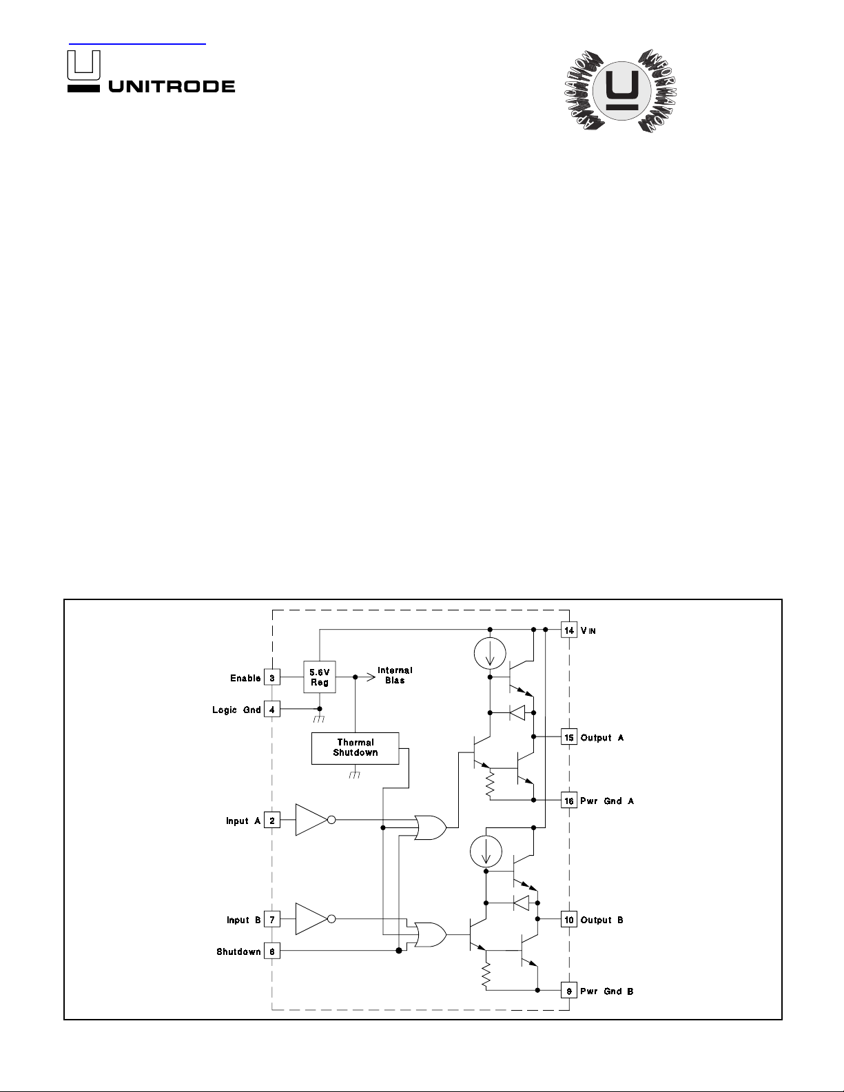
BLOCK DIAGRAM
The UC1708 family of power drivers is made with a high-speed, highvoltage, Schottky p rocess to interface control functions and high-power
switching devices – par t icula rly p ower MOS FETs. Operating over a 5 to
35 volt supply range, thes e devices conta in two inde pendent channels.
The A and B input s are compatible with TTL and CMOS logic families,
but can withstand input voltages as high as V
or sink up to 3A as long as power dissipation limits are not exceeded.
Although each output can be activated independently with its own inputs,
they can be forced low in commo n through the action of either a digital
high signal at the Shutdown terminal or by forcing the Enable terminal
low. The Shutdown ter minal w ill only force the outputs low, it will not effect the behavior of the rest of the device. The Enable terminal effectively
places the device in under-voltage lockout, reducing power consumption
by as much as 90%. During under-voltage and disable (Enable terminal
forced low) conditions, the outputs are held in a self-biasing, low-voltage,
state.
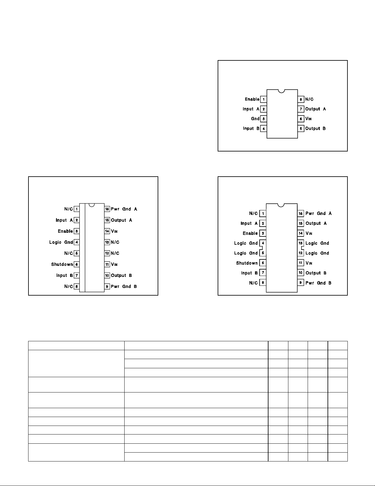
The UC3708 and UC2708 are available in plastic 8-pin MINIDIP and 16pin "bat-wing" DIP packages for commercial operation over a 0
o
+70
C temperatu re range and industrial temperature range of -25oC to
o
+85
C respectively. For operation over a -55oC to +125oC temperature
range, the UC1 708 is available in hermetically sealed 8-pin MINIDIP and
16 pin DIP packages. Surface mount devices are also available .
UC1708
UC2708
UC3708
. Each output can source
IN
o
C to
Note: Shutdown feature a vailable only in JE , NE or DW pac k ag es.
3/97
UDG-92024-1
1
UC1708
UC2708
UC3708
ABSOLUTE MAXIMUM RATINGS
Supply Voltage VIN. . . . . . . . . . . . . . . . . . . . . . . . . . . . . . . . 35V
Output Current (Each Output, Source or Sink)
Steady-State. . . . . . . . . . . . . . . . . . . . . . . . . . . . . . . . . . 0.5A
Peak Transient . . . . . . . . . . . . . . . . . . . . . . . . . . . . . . . . . . 3A
Ouput Voltage . . . . . . . . . . . . . . . . . . . . . . . -0.3 to (VIN + 0.3)V
Enable and Shutdown Inputs . . . . . . . . . . . . . . . . . -0.3 to 6.2V
A and B Inputs . . . . . . . . . . . . . . . . . . . . . . . -0.3 to (VIN + 0.3)V
Operating Junction Temperature (Note 2) . . . . . . . . . . . . 150°C
Storage Temperature Range . . . . . . . . . . . . . . . . -65° to 150°C
Lead Temperature (Soldering, 10 Seconds) . . . . . . . . . . 300°C
(Note 1)
NOTE 1: All voltages are with respect to Logic Gnd pin. All currents are positive into, negative out of, device terminals.
NOTE 2: Consult Unitrode Integrated Circuits databook for
information regarding thermal specifications and limitations of
packages.
SOIC-16 (T op View)
DW Package
CONNECTION DIAGRAMS
DIL-8 (T op Vie w)
J Or N Package
DIL-16 (Top View)
JE or NE Package
Note: In JE package Pin 4 is logic ground. Pins 5, 12,
and 13 are N/C.
ELECTRICAL CHARACTERISTICS:
–55oC<TA<125oC for the UC1708, –25oC<TA<+85oC for the UC2708, and 0oC<TA<70oC for the UC3708. T
PARAMETER TEST CONDITIONS MIN TYP MAX UNITS
Supply Current OutputsLow 18 26 mA
IN
V
A, B and Shutdown Inputs Low
Level
A, B and Shutdown Inputs High
Level
A, B Input Current Low V
A, B Input Current High V
A, B Input Leakage Current High V
Shutdown Input Current Low V
Shutdown Input Current High V
Unless otherwise stated, VIN=10V to 35V, and thes e specificatio ns app ly for:
= T
A
J.
Outputs Hig h 14 18 mA
Enable = 0V 1 4 mA
2.0 V
= 0.4V -1 -0.6 mA
A,B
= 2.4V -200 50
A,B
= 35.3V 200
A,B
SHUTDOWN
SHUTDOWN
V
SHUTDOWN
= 0.4V 20 100
= 2.4V 170 500
= 6.2V 0.6 1.5 mA
2
0.8 V
µ
µ
µ
µ
A
A
A
A
 Loading...