

UNITRODE UC1707, UC2707, UC3707 Technical data
查询UC1707供应商
Dual Channel Power Driver
UC1707
UC2707
UC3707
FEATURES
• Two independent Drivers
• 1.5A Totem Pole Outputs
• Inverting and Non-Inverting Inputs
• 40ns Rise and Fall into 1000pF
• High-Speed, Power MOSFET
Compatible
• Low Cross-Conduction Current Spike
• Analog Shutdown with Optional Latch
• Low Quiescent Current
• 5V to 40V Operation
• Thermal Shutdown Protection
• 16-Pin Dual-In-Line Package
• 20-Pin PLCC and CLCC Package
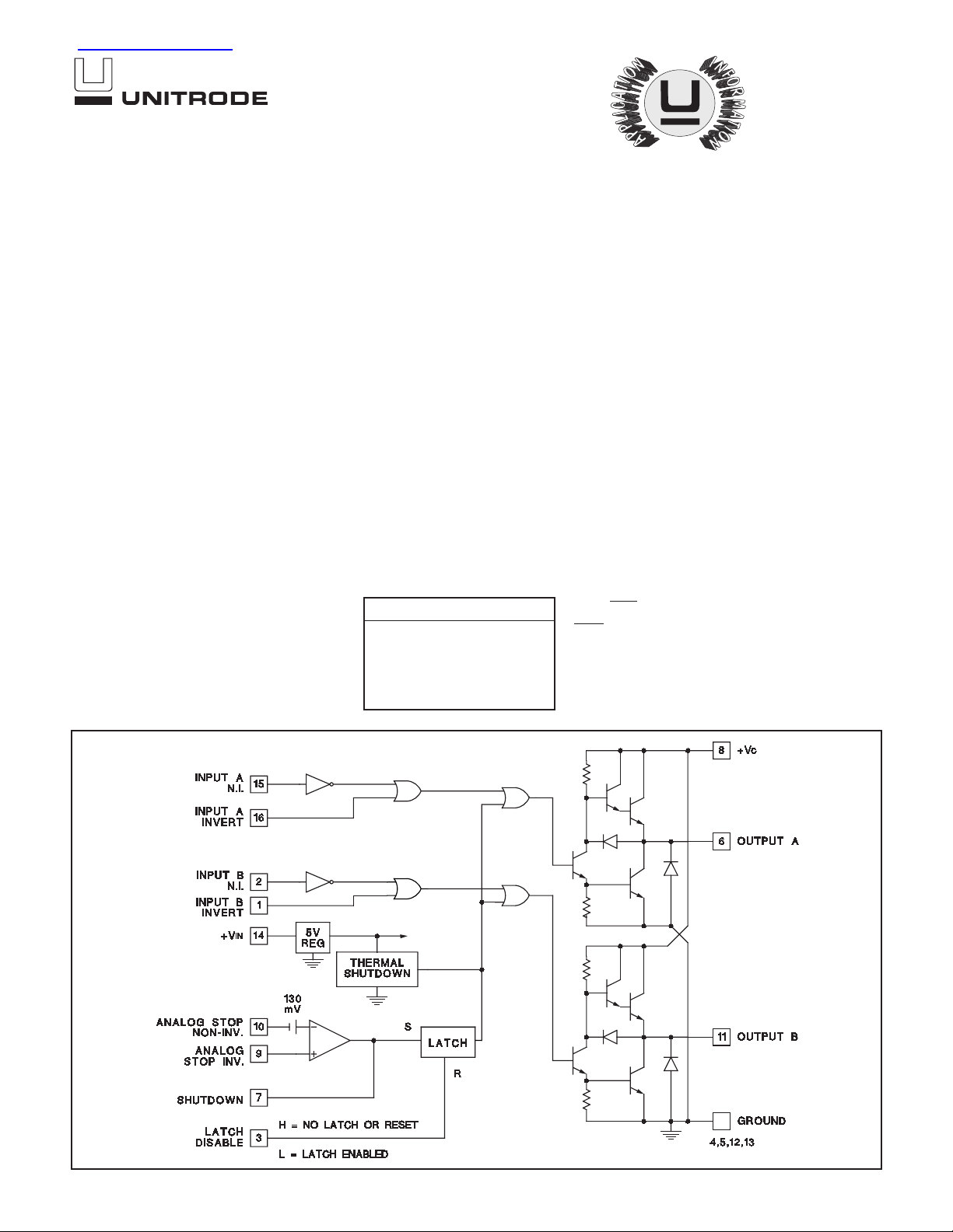
BLOCK DIAGRAM
DESCRIPTION
The UC1707 family of power drivers is made with a high-speed Schottky
process to interface between low-level control functions and high-power
switching devices - particularly power MOSFETs. These devices contain
two independent channels, each of which can be activated by either a high
or low input logic level signal. Each output can source or sink up to 1.5A as
long as power dissipation limits are not exceeded.
Although each output can be activated independently with its own inputs, it
can be forced low in common through the action either of a digital high signal at the Shutdown terminal or a differential low-level analog signal. The
Shutdown command from either source can either be latching or not, depending on the status of the Latch Disable pin.
Supply voltage for both VIN and VC can independently range from 5V to
40V.
These devices are available in two-watt plastic "bat-wing" DIP for operation
over a 0°C to 70°C temperature range and, with reduced power, in a hermetically sealed cerdip for –55°C to +125°C operation. Also available in
surface mount DW, Q, L packages.
TRUTH TABLE (Each Channel)
INV. N.I. OUT OUT = INV and N.I.
H H L OUT
LHH
HLL
LLL
= INV or N.I.
03/99
ABSOLUTE MAXIMUM RATINGS
Supply Voltage, VIN, N/J-Pkg . . . . . . . . . . . . . . . . . . . . . . . 40V
Collector Supply Voltage, VC, N/J-Pkg . . . . . . . . . . . . . . . 40V
Output Current (Each Output, Source or Sink) Steady-State,
N/J-Pkg. . . . . . . . . . . . . . . . . . . . . . . . . . . . . . . . . . . ±500mA
Peak Transient
N-Pkg . . . . . . . . . . . . . . . . . . . . . . . . . . . . . . . . . . . . . . ±1.5A
J-Pkg . . . . . . . . . . . . . . . . . . . . . . . . . . . . . . . . . . . . . . ±1.0A
Capacitive Discharge Energy
N-Pkg . . . . . . . . . . . . . . . . . . . . . . . . . . . . . . . . . . . . . . 20mJ
J-Pkg. . . . . . . . . . . . . . . . . . . . . . . . . . . . . . . . . . . . . . . 15mJ
Digital Inputs (See Note), N/J-Pkg . . . . . . . . . . . . . . . . . . . 5.5V
Analog Stop Inputs, N/J-Pkg . . . . . . . . . . . . . . . . . . . . . . . . VIN
Power Dissipation at TA= 25°C (See Note)
N-Pkg . . . . . . . . . . . . . . . . . . . . . . . . . . . . . . . . . . . . . . . . 2W
J-Pkg . . . . . . . . . . . . . . . . . . . . . . . . . . . . . . . . . . . . . . . . 1W
Power Dissipation at T (Leads/Case) = 25°C (See Note)
N-Pkg . . . . . . . . . . . . . . . . . . . . . . . . . . . . . . . . . . . . . . . . 5W
J-Pkg . . . . . . . . . . . . . . . . . . . . . . . . . . . . . . . . . . . . . . . . 2W
Operating Temperature Range. . . . . . . . . . . . –55°C to +125°C
Storage Temperature Range . . . . . . . . . . . . . –65°C to +150°C
Lead Temperature (Soldering, 10 Seconds) . . . . . . . . . . 300°C
Note: All voltages are with respect to the four ground pins
which must be connected together. All currents are positive
into, negative out of the specified terminal. Digital Drive can exceed 5.5V if input current is limited to 10mA. Consult Packaging section of Databook for thermal limitations and
considerations of package.
UC1707
UC2707
UC3707
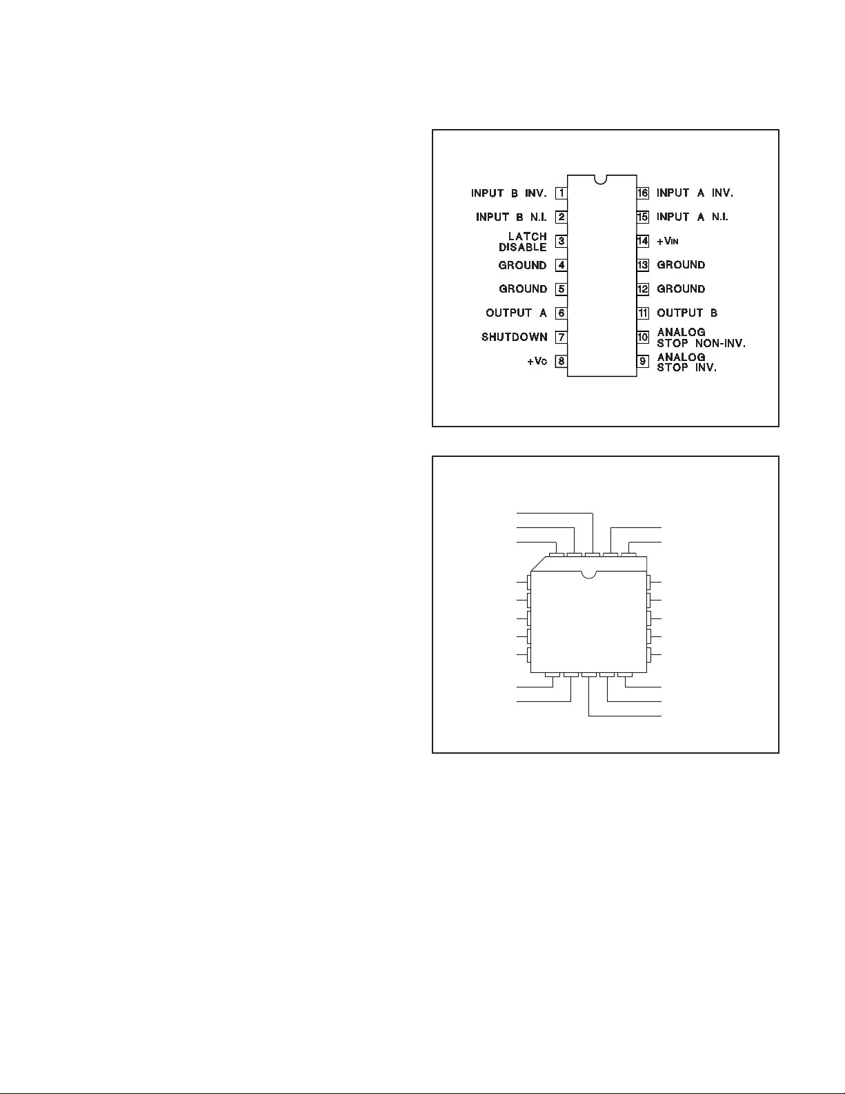
CONNECTION DIAGRAMS
DIL-16, SOIC-16 (TOP VIEW)
J or N Package,
Note: All four ground pins must be connected to a common
ground.
PLCC-20, LCC-20 (TOP VIEW)
Q, L Packages
N/C
INPUT B INV.
INPUT B I.N.
LATCH DISABLE
GROUND
N/C
GROUND
OUTPUT A
SHUTDOWN
VC
3
4
5
6
7
8
91110 12 13
122019
INPUT A INV.
INPUT A NON INV.
18
VIN
17
GROUND
16
N/C
15
GROUND
14
OUTPUT B
ANALOG STOP INV.
ANALOG STOP NON INV.
N/C
2

UC1707
UC2707
UC3707
ELECTRICAL CHARACTERISTICS:
Unless otherwise stated, these specifications apply for TA= –55°C to +125°C for
the UC1707, –25°C to +85°C for the UC2707 and 0°C to +70°C for the UC3707; VIN= VC= 20V. TA=TJ.
PARAMETERS TEST CONDITIONS MIN
V
Supply Current VIN= 40V 12 15 mA
IN
Supply Current VC= 40V, Outputs Low 5.2 7.5 mA
V
C
Leakage Current VIN=0, VC =30V, No Load .05 0.1 mA
V
C
TYP MAX UNITS
Digital Input Low Level 0.8 V
Digital Input High Level 2.2 V
Input Current V
Input Leakage V
Output High Sat., V
Output Low Sat., V
C-VO
O
Analog Threshold V
Input Bias Current V
= 0 –0.06 –1.0 mA
I
= 5V .05 0.1 mA
I
IO= –50mA 2.0 V
= –500mA 2.5 V
I
O
IO= –50mA 0.4 V
= –500mA 2.5 V
I
O
= 0 to 15V 100 130 160 mV
CM
= 0 –10 –20 µA
CM
Thermal Shutdown 155 °C
Shutdown Threshold Pin 7 Input 0.4 1.0 2.2 V
Latch Disable Threshold Pin 3 Input 0.8 1.2 2.2 V
TYPICAL SWITCHING CHARACTERISTICS: V
PARAMETERS TEST CONDITIONS
From Inv. Input to Output
= VC= 20V, TA= 25°C. Delays measured to 10% output change.
IN
OUTPUT CL = UNITS
open 1.0 2.2 nF
Rise Time Delay 40 50 60 ns
10% to 90% Rise 25 40 50 ns
Fall Time Delay 30 40 50 ns
90% to 10% Fall 25 40 50 ns
From N.I. Input to Output
Rise Time Delay 30 40 50 ns
10% to 90% Rise 25 40 50 ns
Fall Time Delay 45 55 65 ns
90% to 10% Fall 25 40 50 ns
Cross-Conduction
V
C
Current Spike Duration
Output Rise 25 ns
Output Fall 0 ns
Analog Shutdown Delay Stop non-Inv. = 0V 180 ns
Stop Inv. = 0 to 0.5V 180 ns
Digital Shutdown Delay 2V Input on Pin 7 50 ns
3
 Loading...