

查询UC2638供应商
Advanced PWM Motor Controller
UC1638
UC2638
UC3638
FEATURES
• Single or Dual Supply Operation
• Accurate High Speed Oscillator
• Differential X5 Current Sense
Amplifier
• Bidirectional Pulse-by-Pulse
Current Limiting
• Programmable Oscillator
Amplitude and PWM Deadband
• Dual 500mA Totem Pole Output
Drivers
• Dual 60V, 50mA Open Collector
Drivers
• Undervoltage Lockout
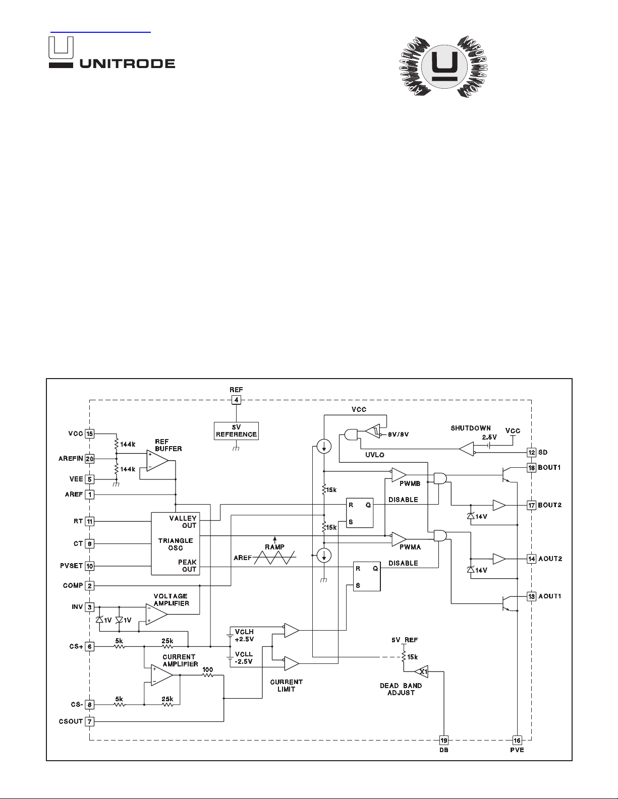
BLOCK DIAGRAM
DESCRIPTION
The UC1638 family of integrated circuits are advanced pulse width modulators intended for a variety of PWM motor drive and amplifier applications requiring either uni-directional or bi-directional drive circuits. Similar in
architecture to the UC1637, all necessary circuitry is included to generate an
analog error signal and modulate two bi-directional pulse train outputs in proportion to the error signal magnitude and polarity.
Key features of the UC1638 include a programmable high speed triangle oscillator, a 5X differential current sensing amplifier, a high slew rate error amplifier, high speed PWM comparators, and two 50mA open collector as well
as two±500mA totem pole output stages. The individual circuit blocks are
designed to provide practical operation to switching frequencies of 500kHz.
Significant improvements in circuit speed, elimination of many external programming components, and the inclusion of a differential current sense amplifier, allow this controller to be specified for higher performance
applications, yet maintain the flexibility of the UC1637. The current sense
amplifier in conjunction with the error amplifier can be configured for average
current feedback.The additional open collector outputs provide a drive signal
continued
1/98
UDG-95048-4
UC1638
UC1638
UC2638
UC2638
UC3638
UC3638
DESCRIPTION (cont.)
for the highside switches in a full bridge configuration.
The programmable AREFIN pin allows for single or dual
supply operation. Oscillator ramp amplitude and PWM
deadband are programmable by tapping a voltage divider off the 5V reference to the appropriate programming input (PVSET or DB).
Additional features include a precision externally available 5V reference, undervoltage lockout, pulse-by-pulse
peak current limiting, and a remote shutdown port. The
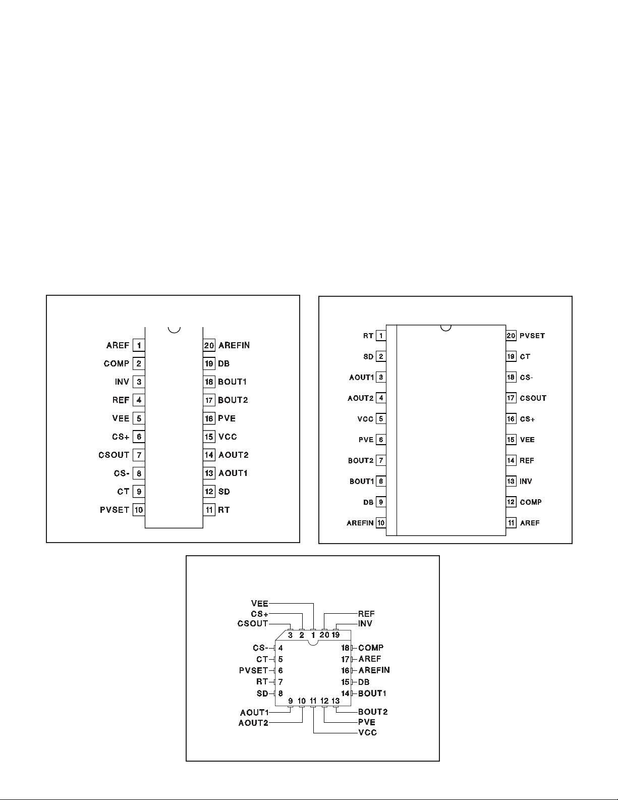
UC1638 family is available in the 20 pin N, DW and J
packages. Consult the factory for other packaging options.
CONNECTION DIAGRAMS
DIL-20 (Top View)
NorJPackage
ABSOLUTE MAXIMUM RATINGS
Supply Voltage VCC (referenced to VEE) .............40V
Output Drivers (AOUT2, BOUT2)
Currents (continuous) ........................±0.25A
Currents (peak) ............................±500mA
REF Output Current ....................Internally Limited
PVSET, DB, RT, INV, REF, CSOUT .............0.3to10V
CS+, CS- .............................VEE–1V to VCC
CT, AREF, AREFIN, COMP, SD ................VEE−0.3
Output Voltage (AOUT1, BOUT1) ....................60V
Storage temperature....................−65°C to +150°C
Junction Temperature...................−55°C to +150°C
Lead temperature (soldering, 10 sec.)..............+300°C
Currents are positive into, negative out of the specified terminal. Consult packaging section of data book for thermal limitation considerations of packages.
SOIC-20 (Top View)
DW Package
PLCC-20 (Top View)
Q Package
2
UC1638
UC2638
UC3638
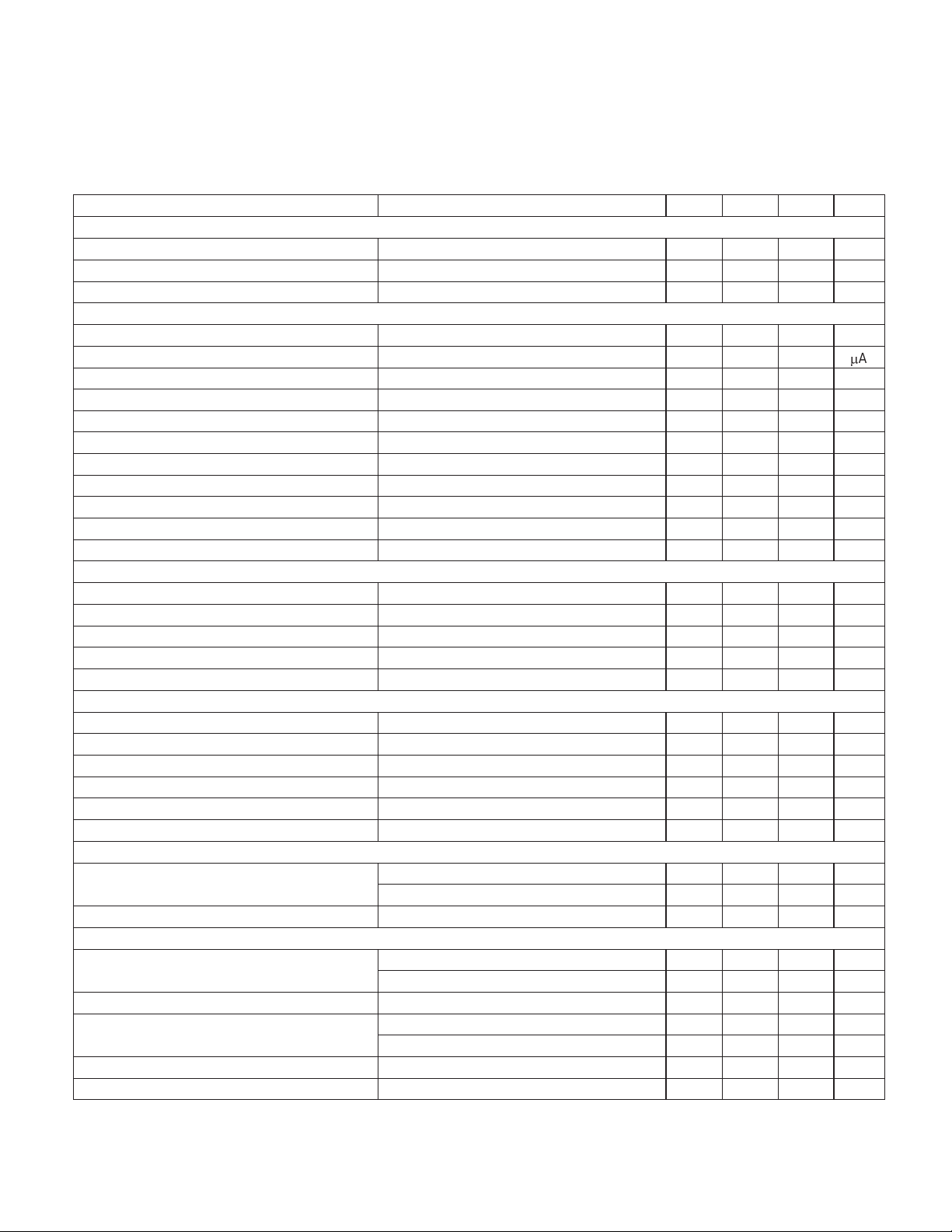
ELECTRICAL CHARACTERISTICS
Unless otherwise specified; VCC = 15V, VEE =–15V, CT = 680pF, RT = 3k,
VPVSET = 1.5V, VCOMP = 0V, VCSOUT = 0V, VDB = REF, VEXTREF = 0V, VSD =
VCC – 3V, TA = −55°C to 125°C for the UC1638, −25°C to 85°C for the UC2638,
0°C to 70°C for the UC3638. TA =TJ.
PARAMETER TEST CONDITIONS MIN TYP MAX UNITS
Overall
Supply Current, Operating 15 23 mA
UVLO Threshold Reference to VEE 9 10 V
UVLO Hysteresis Reference to VEE 1 V
Voltage Amplifier
Input Offset Voltage COMP = 0V −15 0 15 mV
SENSE Bias Current 0 0.5 2
V
Open Loop Gain COMP = −5V to +5V 75 100 dB
CMRR V
CM = −5V to +5V 70 100 dB
PSRR VCM = 0V, VCC − VEE = 10V to 36V 70 90 dB
VOUT High INV = −0.1V, RL = 10k 13 13.6 V
OUT Low INV = +0.1V, RL = 10k −13.8 –13 V
V
Slew Rate Rising and Falling Overdrive =±1V 12 V/µs
Output Source Current COMP Shorted to VEE 5 15 mA
Output Sink Current COMP Shorted to VCC 15 40 mA
Gain Bandwidth Product F
IN = 100kHz, 10mV p-p 1 5 MHz
5V Reference
Output Voltage I
REF = −1mA, TA = 25°C 4.925 5 5.075 V
Output Voltage IREF = −1mA 4.875 5 5.125 V
Load Regulation IREF = −1mA to −10mA −15 2 15 mV
Line Regulation VCC - VEE = 10V to 36V −15 2 15 mV
Short Circuit Current V
REF =0V 15 70 mA
Oscillator
Initial Accuracy T
A = 0°C – 70°C 86 98 110 kHz
Voltage Stability VCC − VEE = 10V to 36V 2 %
Total Variation Line, Temperature 76 98 120 kHz
PVSET Input Bias Current 0.5 3 µA
PVSET Input Voltage Range (Note 1) 0.5 VREF V
Amplitude Limit (Note 1) VEE+3 VCC−3V
AOUT1, BOUT1 Output Drivers
Output Low Voltage I
OUT = 1mA, Ref. to PVE, PVE = 0V 0.9 1.3 V
IOUT = 50mA 1.2 1.8 V
Leakage Current Output Voltage = 50V 0.1 50 µA
AOUT2, BOUT2 Output Drivers
Output High Voltage I
OUT = −20mA, Ref. to PVE, PVE = 0V 12.2 13.5 V
OUT = −100mA, Ref. to PVE, PVE = 0V 12 13.5 V
I
Output High Clamp Level IOUT = −20mA, Ref. to PVE, PVE = VEE 14.4 16.5 V
Output Low Voltage IOUT = 20mA, Ref. to PVE, PVE = 0V 0.4 1 V
OUT = 100mA, Ref. to PVE, PVE = 0V 0.6 2.2 V
I
Output Rise Time COUT = 1nF 50 100 ns
Output Fall Time COUT = 1nF 50 100 ns
m
A
3
 Loading...