

UNITRODE UC2577-ADJ Technical data

查询UC2577T-ADJ供应商
Simple Step-Up Voltage Regulator
FEATURES DESCRIPTION
•
Requires Few External Components
•
NPN Output Switches 3.0A, 65V(max)
•
Extended Input Voltage Range: 3.0V to 40V
•
Current Mode Operation for Improved
Transient Response, Line Regulation, and
Current Limiting
•
Soft Start Function Provides Controlled
Startup
•
52kHz Internal Oscillator
•
Output Switch Protected by Current Limit,
Undervoltage Lockout and Thermal
Shutdown
•
Improved Replacement for LM2577-ADJ
Series
The UC2577-ADJ device provides all the active functions necessary to implement step-up (boost), flyback, and forward converter
switching regulat ors. R equirin g only a few c omponen ts, these simple regula tors efficiently provide up to 60V as a step-up regulator,
and even high er volta ges as a flyback or forwa rd converter regulator.
The UC2577-ADJ features a wide input voltage range of 3.0V to
40V and an adjustable output voltage. An on-chip 3.0A NPN switch
is included with undervoltage lockout, thermal protection circuitry,
and current limiting , as well as soft star t mode operation to reduce
current during startup. Other features include a 52kHz fixed frequency on-chip oscillator with no external components and current
mode control for better line and load regulation.
A standard series of inductors and capacitors are available from
several manufacturers optimized for use with these regulators and
are listed in this data sheet.
UC2577-ADJ
TYPICAL APPLICATIONS
•
Simple Boost and Flyback Converters
•
SEPIC Topology Permits Input Voltage to
be Higher or Lower than Output Voltage
•
Transformer Coupled Forward Regulators
•
Multiple Output Designs
BLOCK DIAGRAM
CONNECTION DIAGRAM
5-Pin TO-220 (Top View)
T Package
Also available in TO-263 Package (TD).
3/97
UDG-94034
UC2577-ADJ
ABSOLUTE MAXIMUM RATINGS
(Note 1)
Supply Voltage . . . . . . . . . . . . . . . . . . . . . . . . . . . . . . . . . . . 45V
Output Switch Voltage . . . . . . . . . . . . . . . . . . . . . . . . . . . . . 65V
Output Switch Current (Note 2) . . . . . . . . . . . . . . . . . . . . . 6.0A
Power Dissipation. . . . . . . . . . . . . . . . . . . . . . Internally Limited
RECOMMENDED OPERATING RANGE
Supply Voltage . . . . . . . . . . . . . . . . . . . . . . . . 3.0V ≤ VIN ≤ 40V
Output Switch Voltage . . . . . . . . . . . . . . . 0V ≤ V
Output Switch Current . . . . . . . . . . . . . . . . . . . . I
Junction Temperature Range. . . . . . . . . . −40°C ≤ TJ ≤ +125°C
SWITCH
SWITCH
Storage Temperature Range . . . . . . . . . . . . . −65°C to +150°C
Lead Temperature (Soldering, 10 sec.) . . . . . . . . . . . . . . 260°C
Maximum Junction Temperature . . . . . . . . . . . . . . . . . . . 150°C
Minimum ESD Rating (C = 100pF, R = 15kΩ) . . . . . . . . . . . 2kV
ELECTRICAL CHARACTERISTICS
Unless otherwise stated, these specifications apply for T
5V, VFB = V
REF
, I
SWITCH
= 0, and TA =TJ.
= −40°C to +125°C, VIN =
A
PARAMETER TEST CONDITIONS MIN TYP MAX UNITS
System Parameters
Output Voltage VIN = 5V to 10V, I
Line Regulation VIN = 3.0V to 10V, I
Load Regulation VIN = 5V, I
Efficiency VIN = 5V, I
Circuit Figure 1
(Note 3)
= 100mA to 800mA 11.40 12.0 12.60 V
LOAD
= 25°C 11.60 12.40 V
T
J
= 300mA 20 100 mV
LOAD
T
= 25°C50mV
J
= 100mA to 800mA 20 100 mV
LOAD
= 25°C50mV
T
J
= 800mA 80 %
LOAD
Device Parameters
Input Supply Current VFB = 1.5V (Switch Off) 7.5 14 mA
= 25°C10mA
T
J
= 2.0A, V
I
SWITCH
T
= 25°C70mA
J
Input Supply UVLO I
= 100mA 2.70 2.95 V
SWITCH
= 25°C2.85V
T
J
Oscillator Frequency Measured at SWITCH Pin, I
T
= 25°C4856kHz
J
Reference Voltage Measured at FB Pin, VIN = 3.0V to 40V, V
= 25°C 1.214 1.246 V
T
J
= 2.0V (Max Duty Cycle) 45 85 mA
COMP
= 100mA 42 52 62 kHz
SWITCH
= 1.0V 1.206 1.230 1.254 V
COMP
Reference Voltage Line Regulation VIN = 3.0V to 40V 0.5 mV
Error Amp Input Bias Current V
Error Amp Transconductance
Error Amp Voltage Gain V
Error Amplifier Output Swing Upper Limit V
Error Amp Output Current
Soft Start Current
Maximum Dut y C yc le V
= 1.0V 100 800 nA
COMP
= 25°C 300 nA
T
J
= −30µA to +30µA, V
I
COMP
T
= 25°C 2400 4800
J
= 0.8V to 1.6V, R
COMP
= 25°C 500 V/V
T
J
= 1.0V 2.0 2.4 V
FB
= 25°C2.2V
T
J
Lower Limit V
= 25°C0.40V
T
J
= 1.0V to 1.5V, V
V
FB
T
= 25°C
J
V
= 1.0V, V
FB
T
= 25°C2.57.5
J
= 1.5V, I
COMP
= 25°C93%
T
J
= 1.5V 0.3 0.55 V
FB
COMP
SWITCH
COMP
COMP
= 0.5V 1.5 5.0 9.5
= 100mA 90 95 %
= 1.0V 1600 3700 5800
COMP
= 1.0MW (Note 4) 250 800 V/V
±
= 1.0V
±
90
130
±
200±400 µA
±
300 µA
≤ 60V
≤ 3.0A
µ
mho
µmho
µA
µA
2
UC2577-ADJ
ELECTRICAL CHARACTERISTICS
Unless otherwise stated, these specifications apply for T
5V, VFB = V
REF
, I
SWITCH
= 0, and TA =TJ.
= −40°C to +125°C, VIN =
A
PARAMETER TEST CONDITIONS MIN TYP MAX UNITS
Device Parameters (cont.)
Switch Transconductance 12.5 A/V
Switch Leakage Current
Switch Saturation Voltage I
NPN Switch Current Limit V
Thermal Resistance
V
T
SWITCH
T
= 65V, VFB = 1.5V (Switch Off) 10 600
SWITCH
= 25°C300
J
= 2.0A, V
J
= 25°C0.7V
= 2.0V 3.0 4.3 6.0 A
COMP
= 2.0V (Max Duty Cycle) 0.5 0.9 V
COMP
Junction to Ambient 65
Junction to Case 2
COMP Pin Current
V
= 0 25 50
COMP
TJ = 25°C40
Note 1: Absolute Maximum Ratings indicate limits beyond which damage to the device may occur. Operating ratings
indicate cond it io ns during which the devi ce is in te nd ed to be functional, but device parameter sp ec if ic at ions may not be
guaranteed under these conditions. For guaranteed specifications and test conditions, see the Electrical Characteristics.
Note 2: Output current cannot be internally limited when the UC2577 is used as a step- up regulator. To prevent damage to
the switch, its current must be externally limited to 6.0A. However, output current is in ternally limited when the UC2577 is
used as a flyback or forward converter regulator.
Note 3. External components such as the diode, inductor, input and output capacitors can affect switching regulator
performance. Wh en the UC2 577 is used as shown in the Test Circuit, sys te m pe rfo rmance will be as specif ie d by t he
system parameters.
Ω
Note 4: A 1.0M
measuring A
resistor is connected to the compensation pin (which is the error amplifier’s output) to ensure accuracy in
In actual applications, this pin’s load resistance should be ≥ 10MΩ, resulting in A
VOL.
that is typically twice
VOL
the guaranteed minimum limit.
µA
µA
°C/W
°
C/W
µ
A
µA
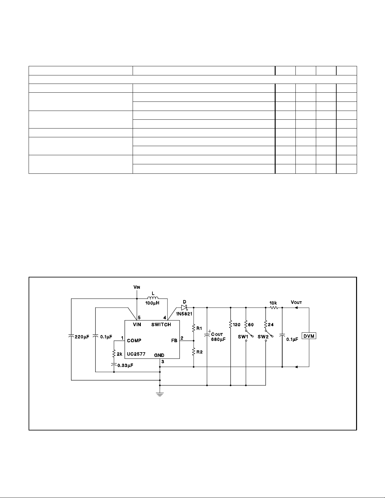
L = 415-0930 (AIE)
D = any manufacturer
C
= Sprague Type 673D
OUT
Electrolytic 680µF, 20V
R1 = 48.7k in series with 511Ω (1%)
R2 = 5.62k (1%)
Figure 1. Circuit Used to Specify System Parameters
3
UDG-94035
 Loading...