SOT
-26
Name
Descript
ion
Power
-
off pin
Switch output pin. Connect external inductor
Pin
Definition
:
6.
Feedback
TS3420
2A, 1.25MHz Synchronous Buck Converter
1. EN
2. Ground
3. Switching Output
4. Input
5. Ground
General Description
TS3420 is a high efficiency monolithic synchronous buck regulator using a constant frequency, current mode
architecture. The device is available in an adjustable version. Supply current with no load is 200uA and drops to
<1uA in shutdown. The 2.8V to 5.5V input voltage range makes TS3420 ideally suited for single Li-Ion, two to
three AA battery-powered applications. 100% duty cycle provides low dropout operation, extending battery life in
portable systems. Switching frequency is internally set at 1.25MHz, allowing the use of small surface mount
inductors and capacitors. The internal synchronous switch increases efficiency and decreases need of an external
schottky diode. Low output voltages are easily supported with the 0.6V feedback reference voltage.
Features
● High Efficiency: Up to 96%
● 2.8V to 5.5V Input Voltage Range
● Output Voltage from 0.6V to VIN
● Short Circuit Protection (SCP)
● Build in Soft-Start Function
● 1.25MHz Constant Frequency Operation
● Up to 2A Output Current
● No Schottky Diode Required in Application
● ≤1uA Shutdown Current
● Current Mode Operation for Excellent Line and
Load Transient Response
Ordering Information
Part No. Package Packing
TS3420CX6 RFG
Note: “G” denote for Halogen Free Product
SOT-26 3Kpcs/ 7” Reel
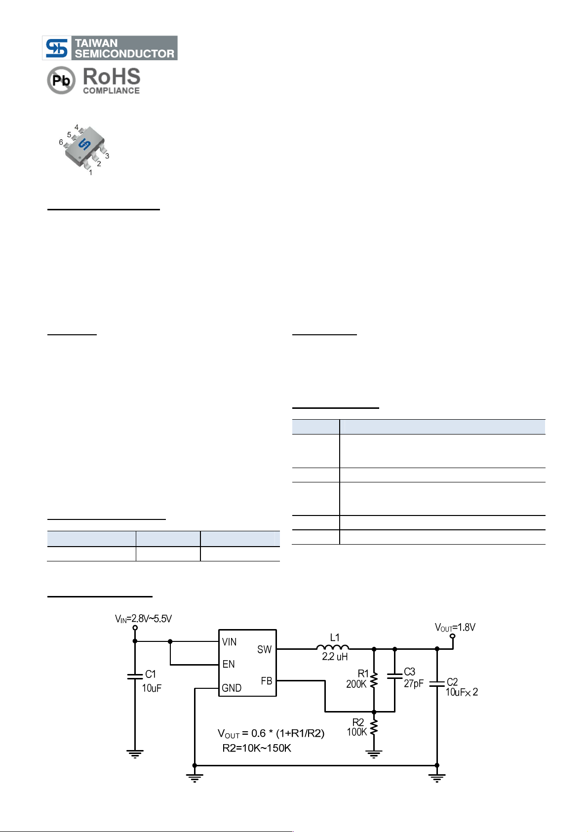
Application Circuit
Application
● Cellular Phones
● Digital Still Cameras
● Portable Electronics
● USB Devices
Pin Description
EN
GND Ground pin
SW
VCC IC power supply pin
FB Output Feedback pin
H:normal operation
L:Step-down operation stopped
here. Minimize trace area at this pin to
reduce EMI.
1/9
Version: A12

△
△
TS3420
2A, 1.25MHz Synchronous Buck Converter
Absolute Maximum Rating
Characteristics Symbol Rating Unit
VIN Pin Voltage VIN VSS - 0.3 to VSS + 6.5 V
Feedback Pin Voltage VFB VSS - 0.3 to VIN + 0.3 V
EN Pin Voltage VEN VSS - 0.3 to VIN + 0.3 V
Switch Pin Voltage VSW VSS - 0.3 to VIN + 0.3 V
Power Dissipation PD ( TJ-TA ) / θJA mW
Storage Temperature Range TST -40 to +150 °C
Operating Temperature Range TOP -40 to +85 °C
Junction Temperature TJ +125 °C
Thermal Resistance from Junction to case θJC 50
Thermal Resistance from Junction to ambient θJA 100
Note: θJA is measured with the PCB copper area of approximately 1 in2(Multi-layer).
o
C/W
o
C/W
Electrical Specifications
(Ta = 25oC, VIN=V
=3.6V unless otherwise noted)
RUN
Characteristics Symbol Conditions Min Typ Max Units
Input Voltage Range VIN 2.8 -- 5.5 V
VIN UVLO Threshold VIN -- 2.2 -- V
VIN UVLO Hysteresis V
Feedback Voltage VFB TA =25℃ 0.588 0.6 0.612 V
Feedback Bias Current IFB VFB=0.65V -- -- ±30 nA
Quiescent Current I
Shutdown Supply Current ISD VEN =0V -- 0.1 1 uA
Switching Current Limit I
Line Regulation
Load Regulation
V
V
Oscillation Frequency F
R
of P-CH MOSFET R
Feedback Bias Current IFB VFB=0.65V -- -- ±30 nA
R
of N-CH MOSFET R
EN pin logic Input Threshold
Voltage
EN Pin Input Current IEN -- ±0.1 ±1 uA
-- 0.35 -- V
IN(hys)
VFB=1V -- 200 350 uA
CCQ
2.2 3 -- A
LIMIT
OUT/VOUT
OUT/VOUT
DSON
DSON
V
V
VIN=2.5V to 5.5V -- 0.4 -- %/V
OSC
I
I
=0.01 to 2A -- 1 -- %
OUT
=300mA 1.0 1.25 1.5 MHz
OUT
VIN=5V -- 120 - mΩ
VIN = 5V (Note) -- 100 - mΩ
-- -- 0.4
ENL
1.5 -- --.
ENH
V
Thermal shutdown TDS -- 150 -- °C
Thermal shutdown Hysteresis TSH -- 30 -- °C
Note: Guaranteed by Design
2/9
Version: A12

2A, 1.25MHz Synchronous Buck Converter
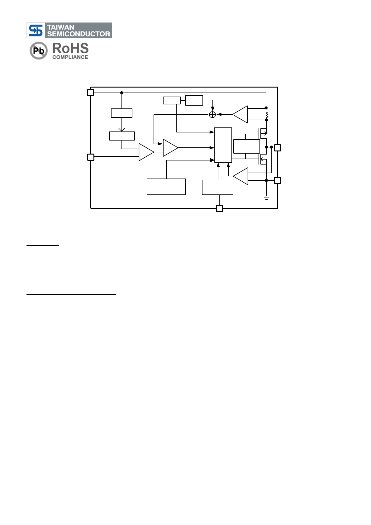
Block Diagram
TS3420
VIN
FB
REF
0.6V
Soft-Star
+
-
-
+
Over-Temperature and
Short-Circuit Protection
OSC
Icomp
SLOPE
COMP
SET
RESET
PWM
LOGIC
Enable Logic
EN
+
Isense
AMP
-
NON-OVERLAP
CONTROL
+
Izero
-
COMP
SW
GND
Function Description
Operation
TS3420 is a monolithic switching mode step-down DC-DC converter. It utilizes internal MOSFETs to achieve high
efficiency and can generate very low output voltage by using internal reference at 0.6V. It operates at a fixed
switching frequency, and uses the slope compensated current mode architecture. This step-down DC-DC
Converter supplies minimum 2A output current at input voltage range from 2.8V to 5.5V.
Current Mode PWM Control
Slope compensated current mode PWM control provides stable switching and cycle-by-cycle current limit for
excellent load and line transient responses and protection of the internal main switch (P-Ch MOSFET) and
synchronous rectifier (N-CH MOSFET). During normal operation, the internal P-Ch MOSFET is turned on for a
certain time to ramp the inductor current at each rising edge of the internal oscillator, and switched off when the
peak inductor current is above the error voltage. The current comparator, I
When the main switch is off, the synchronous rectifier will be turned on immediately and stay on until either the
inductor current starts to reverse, as indicated by the current reversal comparator, I
next clock cycle.
, limits the peak inductor current.
COMP
, or the beginning of the
ZERO
3/9
Version: A12
 Loading...