


TS90071CQ
TS TS90071CQ, TS90071CX, TS90071CX5, TS9007ACQ, TS9007ACX Schematic [ru]
...
TS9007
300mA Low Noise CMOS LDO
1/8 Version: C07
SOT-25
DFN 2x2
SOT-23
General Description
The TS9007 series is 300mA ultra-low-noise LDO especially designed for battery-power RF and wireless
applications. The TS9007 regulator achieves a low 450mV dropout at 300mA load current of 3.3V output, ultra-low
output voltage noise of 15uVrms and PSRR of 57dB at 1KHz.
The TS9007 regulators are also optimized to work with low-ESR and low cost ceramic capacitors reducing the
amount of board space critical in hand-held devices. The TS9007 requires only 0.47uF output capacitor for stability
with and load. The TS9007 consumes less than 1uA in shutdown mode.
Features
● 450mV Dropout at 300mA load (3.3V)
● Low quiescent current: 90µA
● Output voltage ±2%
● Internal current limit and thermal shutdown
● Power saving shutdown mode (<1uA)
● Only need input and output capacitors
● Build-In internal Soft-Start
● Output short-circuit current limit protection
Applications
● Palmtops, PDA and Notebook Computers
● DSC, Handset Camera Modules
● PCMCIA Cards, PC Cameras
● USB Based Portable Devices (MPS, PMP)
● GSM/GPRS/3G RF Transceiver Modules
Ordering Information
Note: Where x denotes voltage option, available are
1= 1.2V
A= 1.5V
D= 1.8V
K= 2.5V
M= 2.7V
N= 2.8V
O= 2.9V
P= 3.0V
S= 3.3V
Contact factory for additional voltage options.
Part No.
Package
Packing
TS9007xCX RF
SOT-23
3Kpcs / 7” Reel
TS9007xCX5 RF
SOT-25
3Kpcs / 7” Reel
TS9007xCQ RF
DFN 2x2
3Kpcs / 7” Reel
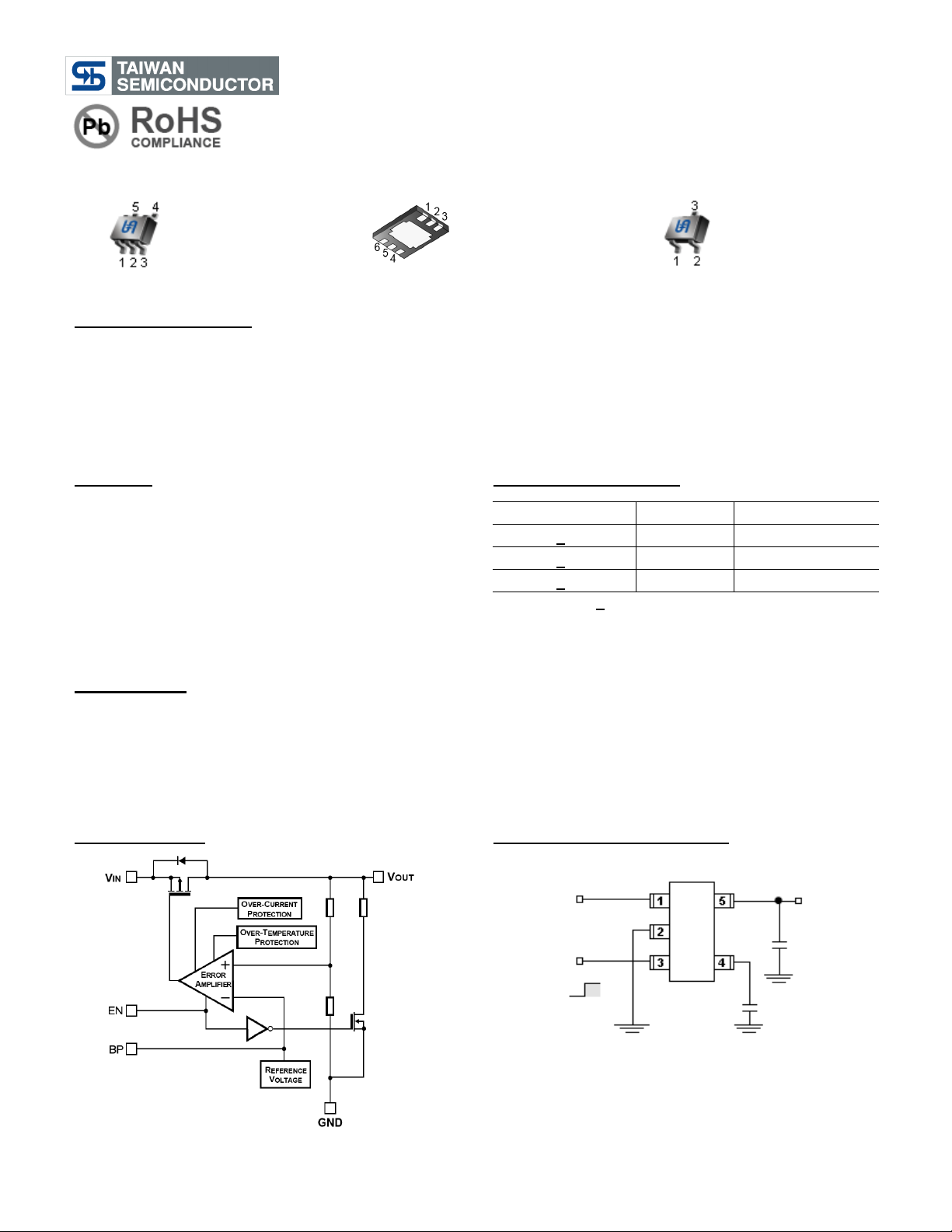
Block Diagram
Typical Application Circuit
EN (Pin 3) may be connected directly to VIN (Pin1)
Low noise operation: C
BYP
=30nF, C
OUT
>0.47uF
Basic operation: C
BYP
=not used, C
OUT
>1uF
C
OUT
0.47uF
C
BYP
30nF
on
off
EN
V
OUT
VIN
Pin Definition:
1. Input
2. Ground
3. Enable
4. Bypass
5. Output
Pin Definition:
1. Input
2. N/C
3. Output
4. N/C
5. Ground
6. Enable
Pin Definition:
1. Ground
2. Output
3. Input

TS9007
300mA Low Noise CMOS LDO
2/8 Version: C07
Absolute Maximum Rating
Parameter
Symbol
Limit
Unit
Supply Voltage
VIN
-0.3 ~ +7
V
Input Supply Voltage (Recommended)
V
OPR
+2 ~ +6
V
Output Short-Circuit Duration
Infinite
Power Dissipation
SOT-25
300
SOT-23
300
DFN 2x2
PD
500
mW
SOT-25
250
SOT-23
300
Thermal Resistance
DFN 2x2
ӨJA
165
°C/W
Junction Temperature Range
TJ
+150
°C
Storage Temperature Range
T
STG
-65 ~ +150
°C
Notes: Stress above the listed absolute rating may cause permanent damage to the device.
Electrical Characteristics (T
A
= 25oC, VIN = (V
OUT
+1V), CIN=C
OUT
=0.47uF, VEN=VIN, unless otherwise noted.)
Parameter
Conditions
Min
Typ
Max
Unit
Output Voltage
VIN =VO + 1V, IO=10mA
-2.0
--
+2
%
Output Current Limit
Short-circuit output
--
200
--
mA
Maximum Output Current
VIN =Vo+1V,
300
--
--
mA
Line Regulation
VIN =(V
OUT
+1V) to 6V, IO=10mA
--
0.3
--
%/V
VIN =Vo+1V, 1mA≤IL≤300mA
V
OUT
≥2.5V
--
0.2
1.0
Load Regulation
VIN =Vo+1V, 1mA≤IL≤200mA
V
OUT
<2.5V
--
0.2
1.0
%
Io=300mA, V
OUT
=Vo - 2%
V
OUT
≥2.5V
--
500
600
Dropout Voltage
Io=200mA, V
OUT
=Vo - 2%
V
OUT
<2.5V
--
800
1000
mV
Shutdown Supply Current
EN=0V
--
0.01
--
uA
Ground Pin Current
Io=0mA
--
90
150
uA
f=100Hz, Io=1mA
--
60
--
f=1KHz, Io=1mA
--
57
--
Ripple Rejection (PSRR)
f=10Hz, Io=1mA
--
45
--
dB
Io=10mA, f=10Hz to 100kHz,
Bypass = 0nF
--
45
--
Output Noise
Io=10mA, f=10Hz to 100kHz,
Bypass = 30nF
--
15
--
uVrms
Shutdown Exit Delay (note 2)
R
LOAD
= 50Ω
--
45
300
uS
EN Logic Low Level
VIN =2.0V to 5.5V
--
--
0.4
EN Logic High Level
VIN =2.0V to 5.5V
1.5
--
VIN
V
EN Input Bias Current
VIN =2.0V to 5.5V
--
--
--
uA
Thermal Shutdown
Shutdown Temperature
--
160
--
o
C
Thermal Shutdown Hysteresis
--
20
--
o
C
Notes:
a. The drop out voltage varies depending on output voltage selection.
Dropout is defined as VIN - V
OUT
when V
OUT
is 100mV below V
OUT
where VIN = Vout+1V for nominal V
OUT
b. Time needed for V
OUT
to reach 90% of final value
TS9007
300mA Low Noise CMOS LDO
3/8 Version: C07
Application Information
Enable / Shutdown
The TS9007 comes with and active-high enable pin that allows the regulator to be enabled. Forcing the enable pin low
disables the regulator and puts it into the shutdown mode. This pin cannot be left floating as it may cause an
undetermined state.
Input / Output Capacitor
It is recommended to use a 0.47uF capacitor on the TS9007 input and a 0.47uF capacitor on the output. For high
regulation performance, larger input capacitor values and lower ESRs provide better noise rejection and line-transient
response. The output noise, load-transient response, stability, and power-supply rejection can be improved by using
large output capacitors. Low ESR ceramic capacitors provide optimal performance and save space.
Power Supply Rejection and Transient Response
The PSRR and transient response can be improved by increasing the values of the input and output bypass
capacitors, and through passive filtering techniques
Function Description
Description
The TS9007 is an ultra-low-noise, low-quiescent current, low-dropout linear regulator. It is supplied in a SOT-25
package for difference applications. This device can supply loads up to 300mA. As shown in the functional block
diagram, the TS9007 consists of a reference and noise bypass circuit, error amplifier, output drive transistor, internal
feedback voltage divider, thermal sensor, and short circuit current limiter. The internal reference is connected to the
error amplifier’s inverting input. The error amplifier compares this reference with the feedback voltage and amplifies
the difference. If the feedback voltage is lower than the reference voltage, the pass=transistor gate is pulled low. This
allows more current to pass to the output and increases the output voltage.
Stability
The TS9007 is a high performance LDO emphasizing stability with low output capacitance. It is able to maintain
stability with an output capacitor can also be increased to optimize performance. The TS9007 will remain stable and in
regulation with no load, unlike many other voltage regulators.
Internal P-Channel Pass Transistor
The TS9007 features a low impedance P-channel MOSFET pass transistor. This provides several advantages over
similar designs using a PNP pass transistor, including low operating power and longer battery life. The TS9007
consumes only 90µA of quiescent current under most conditions.
Output Short-Circuit Current Limit
The TS9007 includes a current limiter, which monitors and controls the pass transistor’s gage voltage, limiting the
output current to about 200mA, for example, in a short-circuit output situation.
Shutdown
The TS9007 also features a low-power active shutdown mode. It has a switch that turns off the device when disabled.
This allows the output capacitor and load to discharge and de-energize the load. In the shutdown mode, the internal
functional blocks, such as voltage reference and the error amplifier, are turned off completely, and the quiescent
current is less than 1µA.
 Loading...