TS1909
MicroPower VFM Boost DC to Dc Converter
1/1 Version: A10
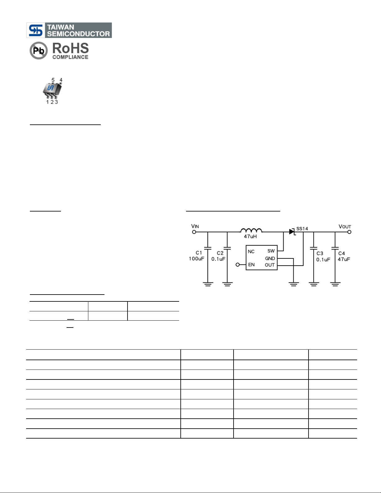
SOT-25
General Description
The TS1909 is a high efficiency VFM Step-up DC/DC converter for small, low input voltage or battery powered
systems with ultra low quiescent supply current. The TS1909 accept a positive input voltage from start-up voltage to
V
OUT
and convert it to a higher output voltage in the 2.5 to 5V range.
The TS1909 combine ultra low quiescent supply current and high efficiency to give maximum battery life. The high
switching frequency and the internally limited peak inductor current permits the use of small, low cost inductors. Only
three external components are needed an inductor a diode and an output capacitor. The TS1909 is suitable to be
used in battery powered equipment where low noise, low ripple and ultra low supply current are required.
Typical applications are pagers, cameras & video camera, cellular telephones, wireless telephones, palmtop
computer, battery backup supplies, battery powered equipment.
Features
● Very Low Supply Current 22µA (Typ.)
● Maximum shutdown current <1µA
● Output Voltage Accuracy ±2.5%
● Output Current up to 100mA
● Low Ripple and Low Noise
● Very Low Start-up Voltage
● High Efficiency Typ. 87% @ V
OUT
=5V
● Few External Components
Ordering Information
Part No.
Package
Packing
TS1909CX5xx RF
SOT-25
3Kpcs / 7” Reel
Note: Where xx denotes voltage option.
Available output: 27=2.7V, 30=3V, 33=3.3V, 50=5V
Typical Application Circuit
Absolute Maximum Rating
Parameter
Symbol
Limit
Unit
VIN Pin Voltage
V
IN
5.5
V
SW Voltage
V
SW
5.5
V
OUT Pin Voltage
V
OUT
5.5
V
Storage Temperature Range
T
STG
-40 to +150
o
C
Operating Junction Temperature Range
TJ
-20 to +100
o
C
Power Dissipation
PD
( TJ-TA ) / θ
JA
mW
Thermal Resistance from Junction to case
θ
JC
110
o
C/W
Thermal Resistance from Junction to ambient
θ
JA
250
o
C/W
Note: θ
JA
is measured with the PCB copper area of approximately 1 inch (Multi-layer) that need connect to GND pin.
Pin Definition:
1. Enable
2. Output
3. N.C
4. Ground
5. SW

TS1909
MicroPower VFM Boost DC to Dc Converter
2/2 Version: A10
Electrical Specifications (Ta = 25
o
C, VIN=5V, EN=VIN, IL=0A unless otherwise noted)
Characteristics
Symbol
Conditions
Min
Typ
Max
Units
Output Voltage Accuracy
∆V
OUT
-2.5
--
+2.5
%
Start-up Voltage (VIN-VF)
(Note 1)
V
START-UP
I
OUT
=1mA, VIN=rising from 0 to 2V
--
0.8
1.2
V
Hold-on Voltage
V
HOLD
I
OUT
=1mA, VIN=falling from 2 to 0V
0.6
--
--
V
Supply Current
I
SUPPLY
No Load
--
22
--
uA
Internal Switch RDSON
RLX
(DSON)
ILX=150mA
--
850
--
mΩ
Internal Leakage Current
ILX
(Leak)
VLX=4V, Forced V
OUT
=3.8V
--
--
0.5
uA
Maximum Oscillator Frequency
F
OSC
--
150
--
KHz
Oscillator Duty On
DON
To be measure on SW pin
--
77
--
%
V
ENH
Driver ON
0.75
--
--
V
Enable Input Threshold
V
ENL
Driver OFF
--
--
0.2
I
ENH
VEN=VIN
--
--
0.1
µA
Enable Input Current
I
ENL
VEN=0V
--
--
-0.1
V
OUT
=2.5V~3.0V, I
OUT
=50mA
--
82
--
%
V
OUT
=3.1V~4.0V, I
OUT
=50mA
--
83
--
%
Efficiency
η
V
OUT
=4.1V~5.0V, I
OUT
=50mA
--
87
--
%
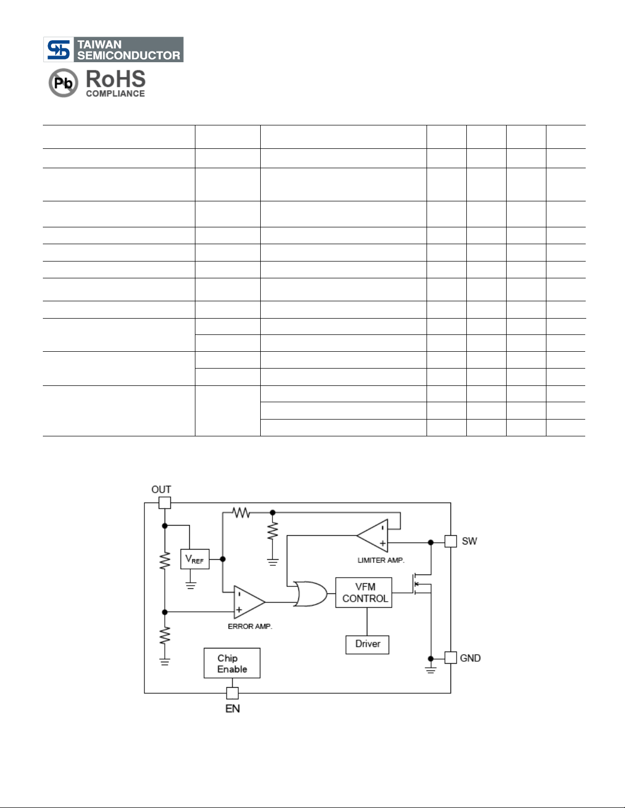
Block Diagram

TS1909
MicroPower VFM Boost DC to Dc Converter
3/3 Version: A10
Detailed Description
The TS1909 architecture is built around a VFM CONTROL logic core, switching frequency is set through a built in
oscillator. TON time is fixed (Typ. 5uS) while T
OFF
time is determined by the error amplifier output, a logic signal coming
from the comparison made by the Error Amplifier Stage between the signal coming from the output voltage divider
network and the internal Band-Gap voltage reference (V
REF
). T
OFF
reaches a minimum (Typ. 1.7uS) when heavy load
conditions are met (Clock frequency 150KHz). An over current conditions, through the internal power switch, causes a
voltage drop VLX=R
DSON
x ISW and the VLX limiter block forces the internal switch to be off, so narrowing TON time
and limiting internal power dissipation. In this case the switching frequency may be higher than the 150KHz set by the
internal clock generator.
VFM control ensures very low quiescent current and high conversion efficiency even with very light loads. Since the
Output Voltage pin is also used as the device Supply Voltage, the versions with higher output voltage present an
higher internal supply voltage that results in lower power switch R
DSON
, slightly greater output power and higher
efficiency. Moreover, bootstrapping allows the input voltage to sag to 0.6V (at IOUT=1mA) once the system is started.
If the input voltage exceeds the output voltage, the output will follow the input, however, the input or output voltage
must not be forced above 5.5V.
Application Information
Input/Output Capacitor Selection
The Output Ripple Voltage, as well as the Efficiency, is strictly related to the behavior of these elements. The output
ripple voltage is the product of the peak inductor current and the output capacitor Equivalent Series Resistance (ESR).
Best performances are obtained with good high frequency characteristics capacitors and low ESR. The best
compromise for the value of the Output Capacitance is 47µF Tantalum Capacitor; Lower values may cause higher
Output Ripple Voltage and lower Efficiency without compromising the functionality of the device. An Input Capacitor is
required to compensate, if present, the series impedance between the Supply Voltage Source and the Input Voltage of
the Application.
Inductor Selection
A 47µH inductor is recommended for most TS1909 applications. However, the inductance value is not critical, and the
TS1909 will work with inductors in the 33µH to 120µH.
Diode Selection
Schottky diodes with higher current ratings usually have lower forward voltage drop, larger diode capacitance and fast
reverse recovery, it is the ideal choices for TS1909 applications. The forward voltage drop of a Schottky diode
represents the conduction losses in the system, while the diode capacitance (CT or CD) represents the switching
losses. For diode selection, both forward voltage drop and diode capacitance need to be considered.
PCB layout guide
When laying out the PC board, the following suggestions should be taken to ensure proper operation of the TS1909.
These items are also illustrated graphically in below. The power traces, including the GND trace, the SW trace and the
VCC trace should be kept short, direct and wide to allow large current flow. Put enough multiply-layer pads when they
need to change the trace layer. Do not trace signal line under inductor.
 Loading...