

Page 1

T
S
1
T
S
1
T
S
1
Description
2
2
2
8
8
8
M
M
M
~
~
~
4
4
4
G
G
G
M
M
M
M
M
M
C
C
C
4
4
4
MMCplus
Features
TS128MMC4 ~ TS4GMMC4 is a 128MB ~ 4GB
MMCplus memory card. It’s a fastest, low-power,
highly integration memory card. It is designed to
provide an inexpensive, mechanically robust storage
medium in card form for multimedia consumer
applications and mobile devices (handheld PCs,
digital cameras, MP3 players, etc.) to store, copy,
and move data at high-speed transfer rate.
Placement
Storage Capacity: 128MB ~ 4GB
Operating Voltage: 2.7~3.6V
Support clock frequencies: 0-20 MHz, 0-26 MHz, or
0-52 MHz
Support different Bus width: x1, x4, x8
Operating Temperature: -25°C ~ 85°C
Compatible with Multimedia Card system specification
version 4.2
Form Factor: 32mm x 24mm x 1.4mm
Front Back
S: Power Supply; I:Input; O:Output; PP:Push-Pull; OD:Open-Drain; NC:Not Connected
Pin Definition
MMC Mode
Pin No.
Name Type Description
1 DAT3 I/O/PP Data
2 CMD I/O/PP/OD Command/Response
3 VSS1 S Ground
4 VDD S Power supply
5 CLK I Clock
6 VSS2 S Ground
7 DAT0 I/O/PP
8 DAT1 I/O/PP Data
9 DAT2 I/O/PP Data
10 DAT4 I/O/PP Data
11 DAT5 I/O/PP Data
12 DAT6 I/O/PP Data
13 DAT7 I/O/PP Data
Data
Transcend Information Inc.
1
Page 2
T
S
1
2
8
M
~
4
G
M
T
S
1
2
8
M
~
4
T
S
1
2
8
M
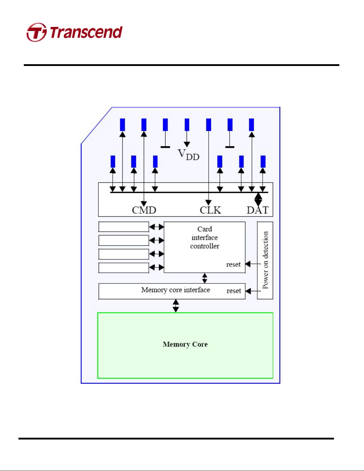
Multimedia Card Architecture
~
4
G
G
M
M
M
M
M
C
4
4
4
C
C
MMCplus
Transcend Information Inc.
2
Page 3
T
S
1
2
8
M
~
4
G
M
M
T
S
1
2
8
M
~
4
G
T
S
1
2
8
M
~
4
Electrical DC Characteristics
•General bus operating conditions
Parameter Symbol Min Max Unit
Peak voltage on all lines -0.5
Input Leakage Current (before initialization sequence
and/or the internal pull up resistors connected)
Input Leakage Current (after initialization sequence and
the internal pull up resistors disconnected)
G
M
M
M
M
C
C
4
4
C
4
All Inputs
All Outputs
-100
-10
MMCplus
3.6 V
100 uA
10 uA
Output Leakage Current (before initialization sequence) -100
Output Leakage Current (after initialization sequence) -10
•MMC high-voltage power supply voltage
Parameter Symbol Min Max Unit
Supply voltage VDD 2.7
Supply voltage differentials (VSS1, VSS2) -0.5
• Bus Signal Line Load
The total capacitance CL of each line of the MultiMedia Card bus is the sum of the bus master capacitance
C
, the bus capacitance C
HOST
C
= C
L
HOST
+ C
BUS
+ C
CARD
itself and the capacitance C
BUS
of the card connected to this line:
CARD
100 uA
10 uA
3.6 V
0.5 V
Parameter Symbol Min Max Unit Remark
Pull-up resistance for CMD R
Pull-up resistance for DAT0-7 R
Internal pull up resistance DAT1-DAT7 R
Bus signal line capacitance CL
Single card capacitance C
Maximum signal line inductance
Transcend Information Inc.
4.7
CMD
50
DAT
50
int
CARD
3
100 KOhm to prevent bus floating
100 KOhm to prevent bus floating
150 kOhm
30 pF Single card
7 pF
16 nH f
to prevent unconnected
lines floating
<= 52 MHz
PP
Page 4

T
S
1
2
8
M
~
4
G
M
M
T
S
1
2
8
M
~
4
G
T
S
1
2
8
M
~
4
• Open-drain mode bus signal level
Parameter Symbol Min. Max. Unit Condition
G
M
M
M
M
C
C
C
4
4
4
(Ta=-25℃ to 85℃,V
MMCplus
=2.7V to 3.6V)
DDH
Output HIGH voltage V
Output LOW voltage VOL 0.3 V IOL = 2 mA
• Push-pull mode bus signal level—high-voltage MultiMedia Card
Parameter Symbol Min. Max. Unit Condition
Output HIGH voltage VOH 0.75*V
Output LOW voltage VOL 0.125*V
Input HIGH voltage VIH 0.625*V
Input LOW voltage VIL VSS-0.3 0.25*VDD V
V
OH
-0.2 V V IOH = -100 μA
DD
(Ta=-25℃ to 85℃,V
DD
DD
V IOH=-100 μA @VDD min
DD
VDD + 0.3 V
V IOL=100 μA @VDD min
DDH
=2.7V to 3.6V)
Transcend Information Inc.
4
Page 5

T
S
1
2
8
M
~
4
G
M
M
T
S
1
2
8
M
~
4
G
T
S
1
2
8
M
~
4
Electrical AC Characteristics
• Card interface timings
Parameter Symbol Min. Max. Unit Notes
Clock Frequency (Data Transfer Mode) fpp 0 26/52 MHz
Clock Frequency (Identification Mode) fOD 0 400 KHz Tolerance: +20KHz
G
M
M
M
M
C
C
C
4
4
4
(Ta=-25℃ to 85℃,V
<= 30 pF
C
L
Tolerance: +100KHz
MMCplus
=2.7V to 3.6V)
DDH
Clock Low Time t
Clock Rise Time t
Clock Fall Time t
Inputs CMD, DAT (referenced to CLK)
Input Set-up Time t
Input Hold Time tIH 3 ns CL<=30pF
Outputs CMD, DAT (referenced to CLK)
Input Set-up Time t
Input Hold Time t
Signal Rise Time t
Signal Fall Time t
NOTE 1. All timing values are measured relative to 50% of voltage level
NOTE 2. A Multimedia Card shall support the full frequency range from 0-26Mhz, or 0-52MHz
NOTE 3. Rise and fall times are measured from 10%-90% of voltage level
NOTE 4. Rise and fall times are measured from 10%-90% of voltage level
6.5 ns CL <= 30 pF
WL
3 ns CL <= 30 pF
TLH
3 ns CL <= 30 pF
THL
3 ns CL<=30pF
ISU
5 ns CL<=30pF
OSU
5 ns CL<=30pF
OH
C
3 ns
rise
3 ns CL<=30pF
fall
<=30pF
L
Note: Data must always be sampled on the rising edge of the clock.
Transcend Information Inc.
5
Page 6

T
S
1
2
8
M
~
4
G
M
M
T
S
1
2
8
M
~
4
G
T
S
1
2
8
M
~
4
• Backward-compatible card interface timing
Parameter Symbol Min. Max. Unit Notes
Clock Frequency (Data Transfer Mode) fpp 0 20 MHz
Clock Frequency (Identification Mode) fOD 0 400 KHz
G
M
M
M
M
C
C
C
4
4
4
(Ta=-25℃ to 85℃,V
=2.7V to 3.6V)
DDH
C
<= 30 pF
L
MMCplus
Clock Low Time t
Clock Rise Time t
Clock Fall Time t
Inputs CMD, DAT (referenced to CLK)
Input Set-up Time t
Input Hold Time tIH 3 ns CL<=30pF
Outputs CMD, DAT (referenced to CLK)
Input Set-up Time t
Input Hold Time tOH 5 ns CL<=30pF
Signal Rise Time t
Signal Fall Time t
NOTE 1. All timing values are measured relative to 50% of voltage level
NOTE 2. Clock rise and fall times are measured from V
6.5 ns C
WL
3 ns C
TLH
3 ns C
THL
3 ns CL<=30pF
ISU
5 ns CL<=30pF
OSU
3 ns
rise
3 ns CL<=30pF
fall
to V
of voltage level
IL
IH
<= 30 pF
L
<= 30 pF
L
<= 30 pF
L
C
<=30pF
L
Transcend Information Inc.
6
Page 7
T
S
1
2
8
M
~
4
G
M
M
T
S
1
2
8
M
~
4
G
T
S
1
2
8
M
~
4
Reliability and Durability
Temperature Operation: -25°C / 85°C
Moisture and corrosion Operation: 25°C / 95% rel. humidity
ESD protection Contact Pads:
UV light exposure UV: 200nm, 15Ws/cm² according to ISO 7816-1
Visual inspection
Shape and form
Above technical information is based on MMC4.2 standard specification and tested to be reliable, but SPI mode would not be
supported. Transcend makes no warranty, either expressed or implied, as to its accuracy and assumes no liability in
connection with the use of this product. Transcend reserves the right to make changes in specifications at any time without
prior notice
G
M
M
C
M
C
M
Storage: -40°C (168h) / 85°C (500h)
Junction temperature: max. 95°C
Stress: 40°C / 93% rel. hum./500h
Salt Water Spray: 3% NaCl/35C; 24h acc. MIL STD Method 1009
+/-4kV, Human body model according to ANSI EOS/ESD-S5.1-1998
Non Contact Pads area:
+/-8kV(coupling plane discharge)
+/-15kV(air discharge)
Human body model according to IEC61000-4-2
No warp page; no mold skin; complete form; no cavities surface smoothness sigma
-0.1 mm/cm² within contour; no cracks; no pollution (fat, oil dust, etc.)
C
4
4
4
MMCplus
Transcend Information Inc.
7
 Loading...