

Page 1
T
S
2
G
~
8
G
G
~
~
8
8
G
G
G
T
S
2
T
S
2
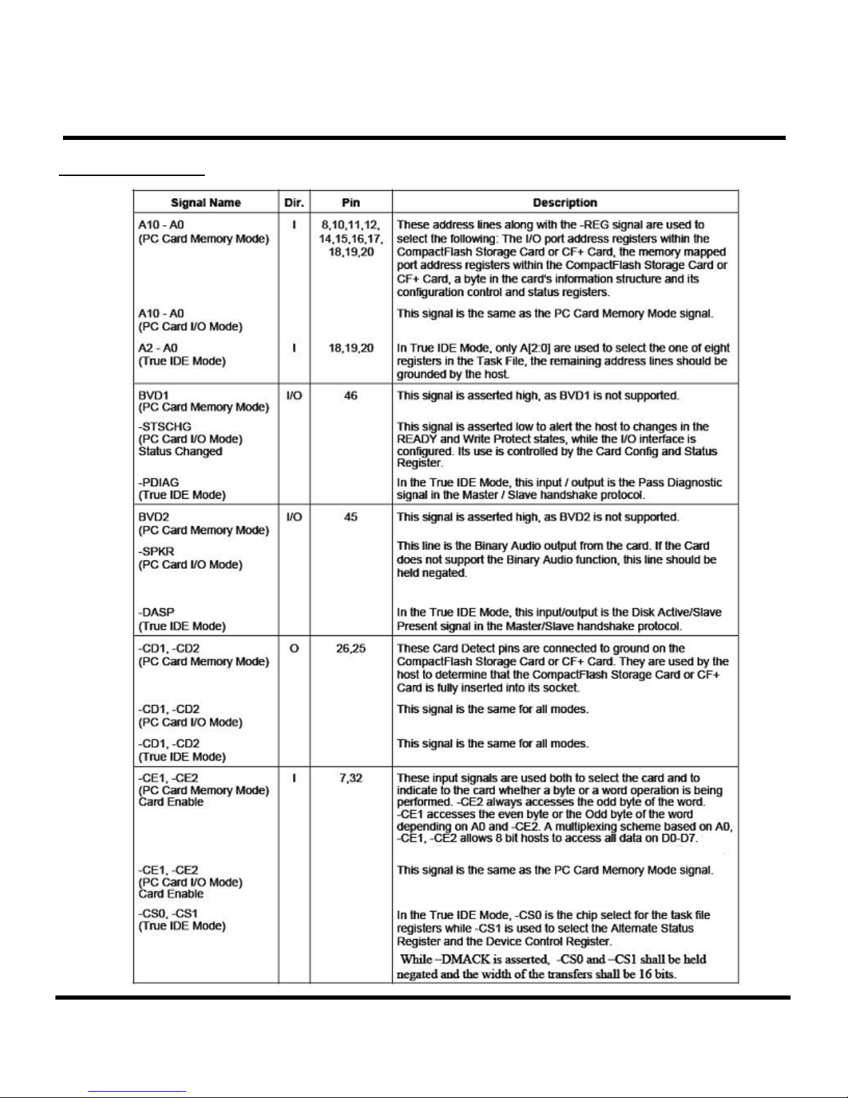
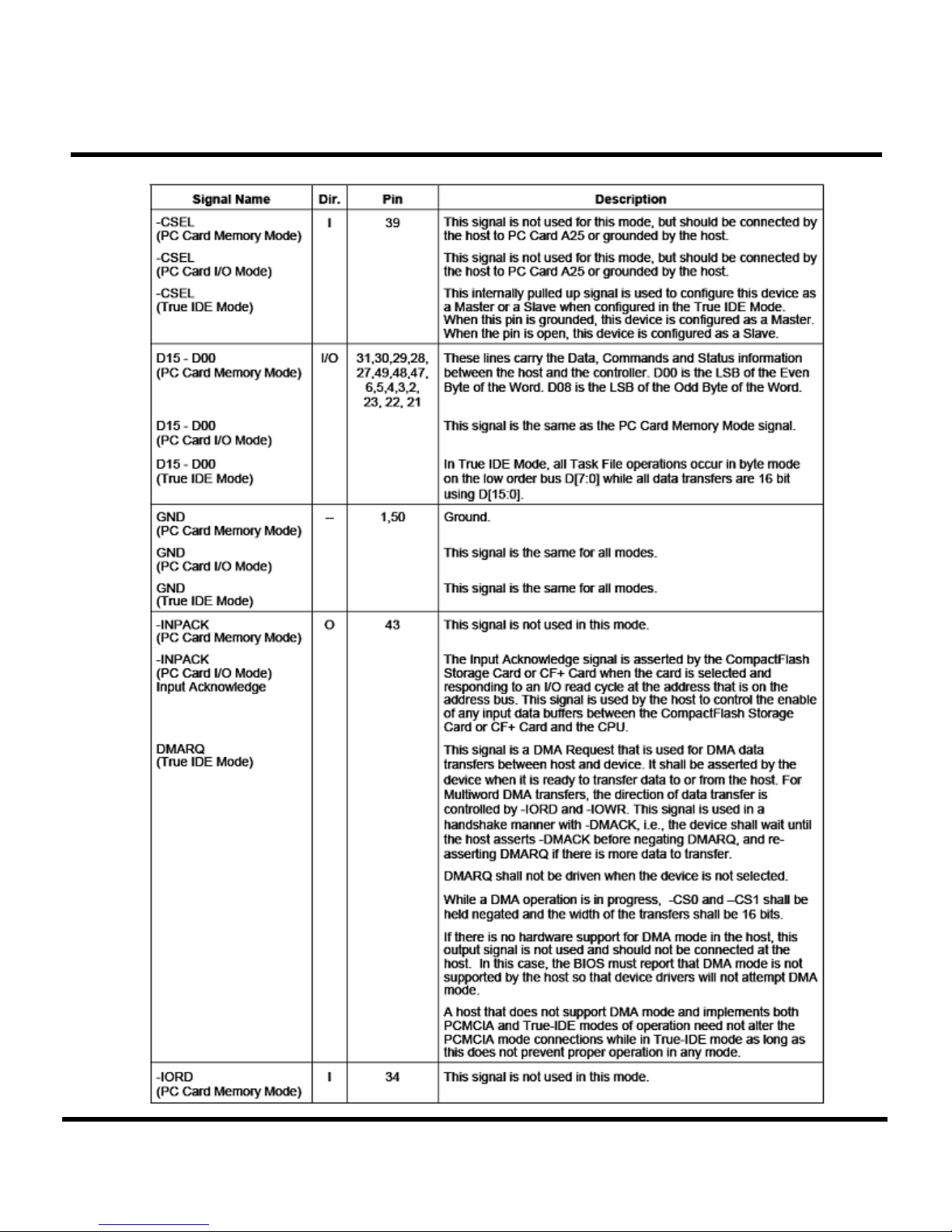
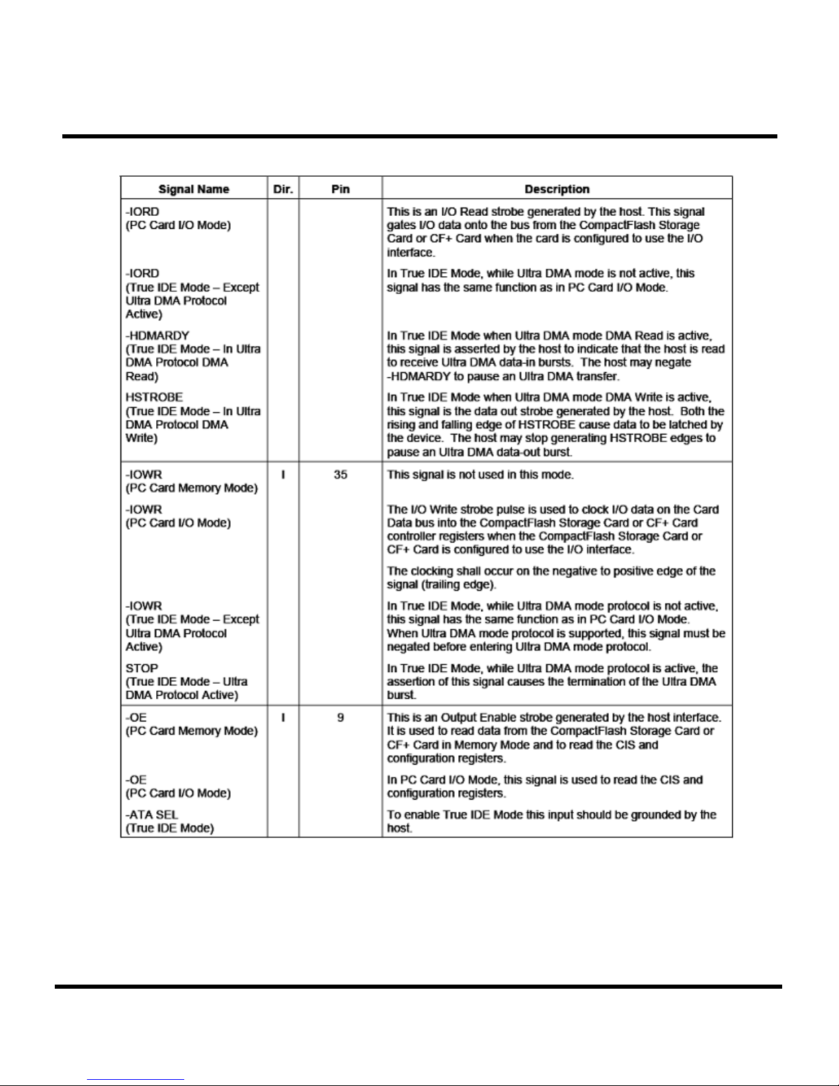
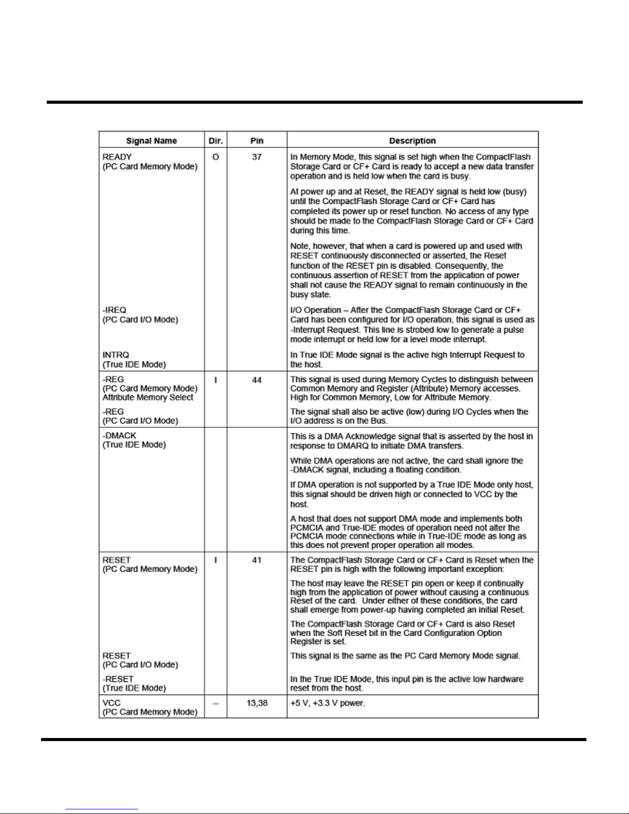
Description
C
C
C
F
F
F
2
2
2
6
6
6
6
6
6
Features
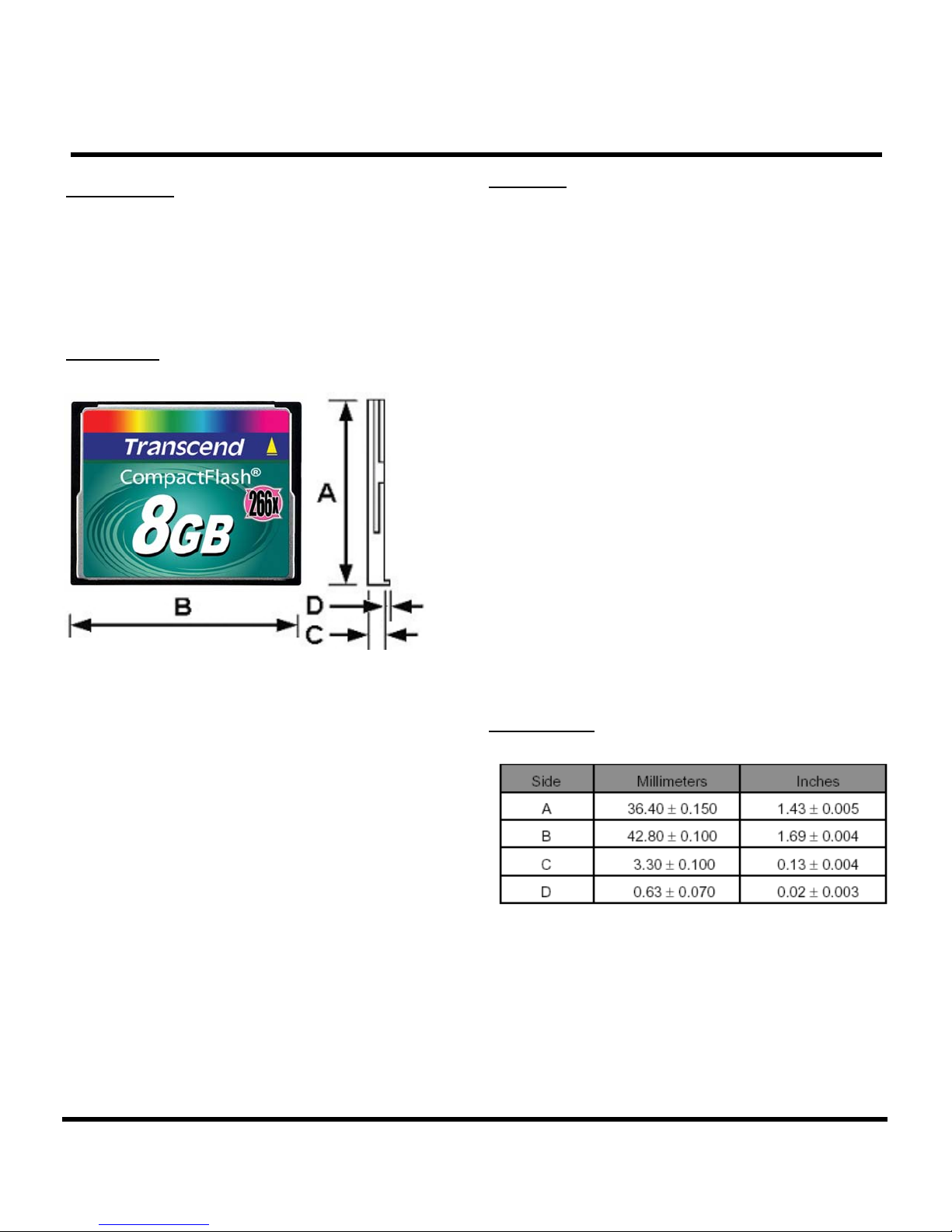
266X CompactFlash Card
The Transcend CF 266X is a High Speed Compact
Flash Card with high quality Flash Memory assembled
on a printed circuit board.
Placement
• CompactFlash Specification Version 4.1 Complaint
• RoHS compliant products
• Single Power Supply: 3.3V±5% or 5V±10%
o
• Operating Temperature: -25
• Operation Modes:
PC Card Memory Mode
PC Card IO Mode
True IDE Mode
• True IDE Mode supports
Ultra DMA Mode 0 to Mode 4
MultiWord DMA Mode 0 to Mode 4
PIO Mode 0 to Mode 6
• Durability of Connector: 10,000 times
• Support S.M.A.R.T (Self-defined)
• Support Wear-Leveling to extend product life
• Compliant to CompactFlash, PCMCIA, and ATA
C to 85oC
Transcend Information Inc.
standards
Dimensions
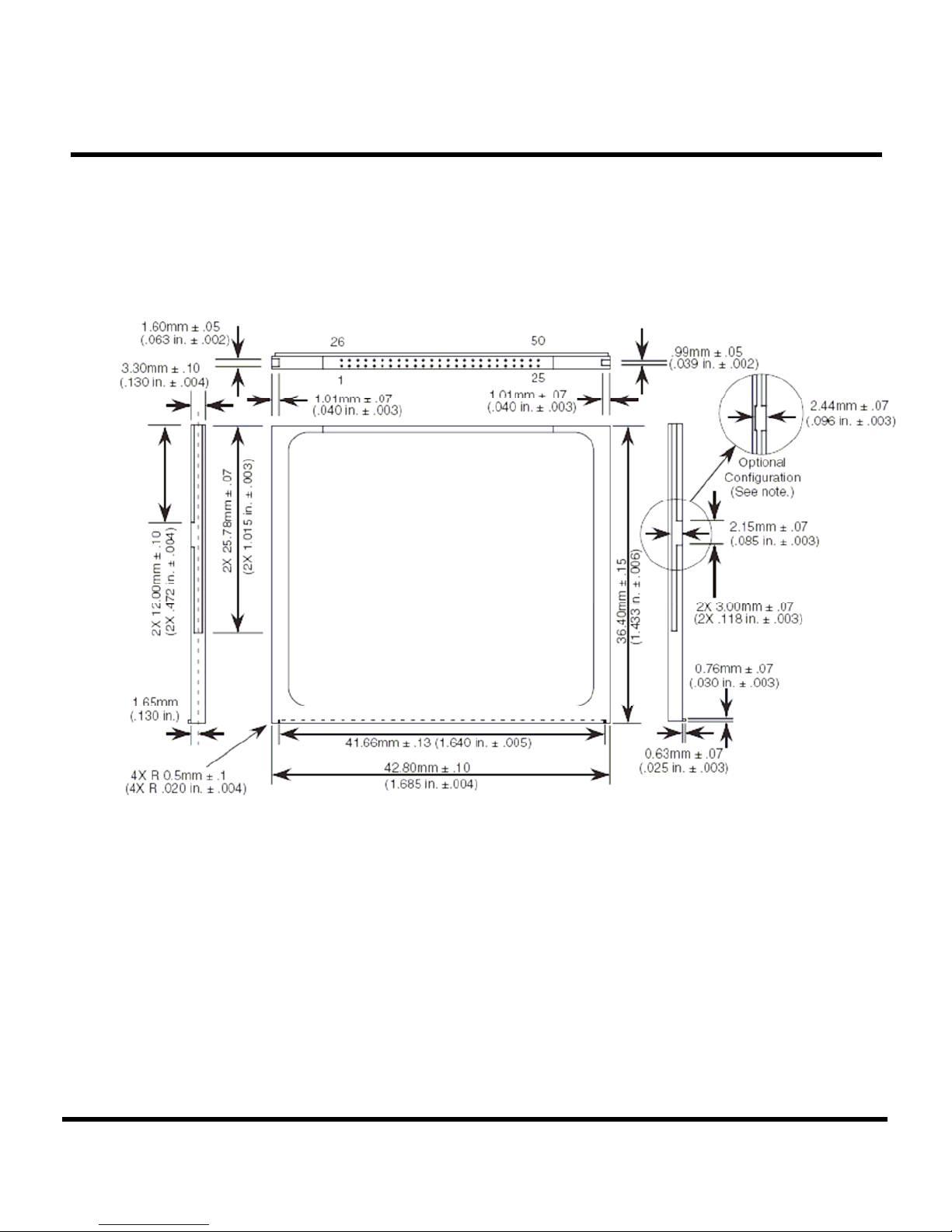
1
Page 2
T
T
T
S
2
G
~
8
G
C
F
2
6
6
S
S
2
2
G
G
~
~
8
8
G
G
C
C
F
F
2
2
6
6
6
6
266X CompactFlash Card
Transcend
Transcend Information Inc.
2
Page 3
T
S
2
G
~
8
G
T
S
2
G
T
S
2
G
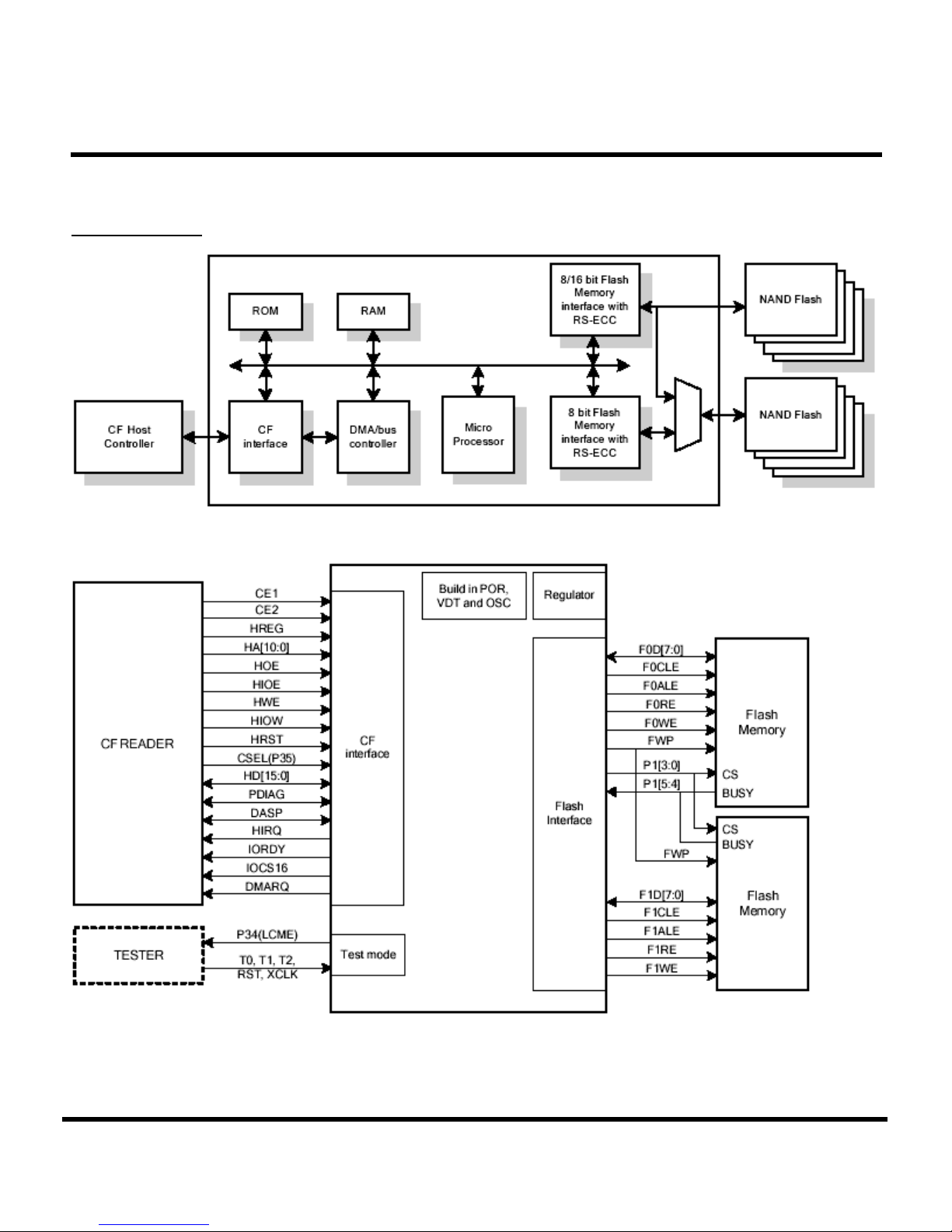
Block Diagram
~
~
8
8
G
G
C
C
C
F
F
F
2
2
2
6
6
6
6
6
6
266X CompactFlash Card
Transcend Information Inc.
3
Page 4
T
S
2
G
~
8
G
C
F
2
6
6
T
S
2
G
~
8
G
C
T
S
2
G
~
8
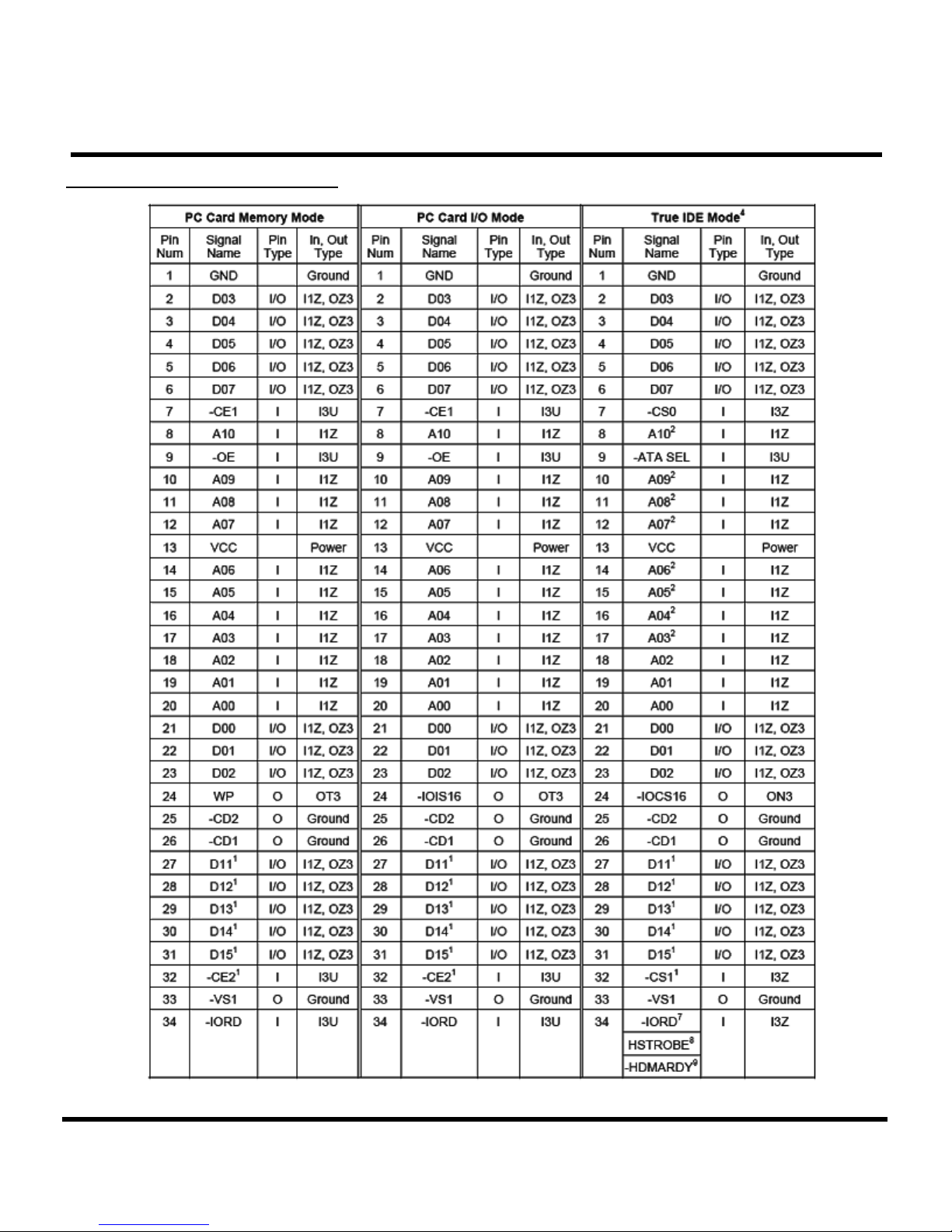
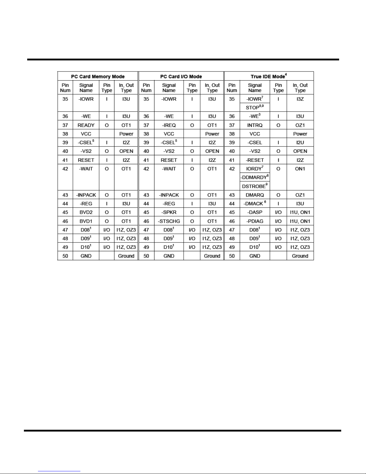
Pin Assignments and Pin Type
G
C
F
F
2
2
6
6
6
6
266X CompactFlash Card
Transcend Information Inc.
4
Page 5
T
T
T
S
S
S
2
2
2
G
G
G
~
~
~
8
8
8
G
G
G
C
C
C
F
F
F
2
2
2
6
6
6
6
6
6
266X CompactFlash Card
Note: 1) These signals are required only for 16 bit accesses and not required when installed in 8 bit
systems. Devices should allow for 3-state signals not to consume current.
2) The signal should be grounded by the host.
3) The signal should be tied to VCC by the host.
4) The mode is optional for CF+ Cards, but required for CompactFlash Storage Cards.
5) The -CSEL signal is ignored by the card in PC Card modes. However, because it is not
pulled upon the card in these modes, it should not be left floating by the host in PC Card
modes. In these modes, the pin should be connected by the host to PC Card A25 or
grounded by the host.
6) If DMA operations are not used, the signal should be held high or tied to VCC by the host. For
proper operation in older hosts: while DMA operations are not active, the card shall ignore
this signal,including a floating condition
7) Signal usage in True IDE Mode except when Ultra DMA mode protocol is active.
8) Signal usage in True IDE Mode when Ultra DMA mode protocol DMA Write is active.
9) Signal usage in True IDE Mode when Ultra DMA mode protocol DMA Read is active.
10) Signal usage in PC Card I/O and Memory Mode when Ultra DMA mode protocol DMA Write is active.
11) Signal usage in PC Card I/O and Memory Mode when Ultra DMA mode protocol DMA Read is active.
12) Signal usage in PC Card I/O and Memory Mode when Ultra DMA protocol is active.
Transcend Information Inc.
5
Page 6
T
S
2
G
~
8
G
C
F
T
S
2
G
~
8
G
~
8
G
G
T
S
2
Signal Description
C
C
F
F
2
2
2
6
6
6
6
6
6
266X CompactFlash Card
Transcend Information Inc.
6
Page 7
T
T
T
S
S
S
2
2
2
G
G
G
~
~
~
8
8
8
G
G
G
C
C
C
F
F
F
2
2
2
6
6
6
6
6
6
266X CompactFlash Card
Transcend Information Inc.
7
Page 8
T
T
T
S
S
S
2
2
2
G
G
G
~
~
~
8
8
8
G
G
G
C
C
C
F
F
F
2
2
2
6
6
6
6
6
6
266X CompactFlash Card
Transcend Information Inc.
8
Page 9
T
T
T
S
S
S
2
2
2
G
G
G
~
~
~
8
8
8
G
G
G
C
C
C
F
F
F
2
2
2
6
6
6
6
6
6
266X CompactFlash Card
Transcend Information Inc.
9
Page 10

T
T
T
S
S
S
2
2
2
G
G
G
~
~
~
8
8
8
G
G
G
C
C
C
F
F
F
2
2
2
6
6
6
6
6
6
266X CompactFlash Card
Transcend Information Inc.
10
Page 11
T
S
2
G
~
8
G
C
F
2
6
6
T
S
2
G
~
8
G
C
T
S
2
G
~
8
Electrical Specification
The following tables indicate all D.C. Characteristics for the CompactFlash Storage Card. Unless
otherwise stated, conditions are:
Vcc = 5V ±10%
Vcc = 3.3V ± 5%
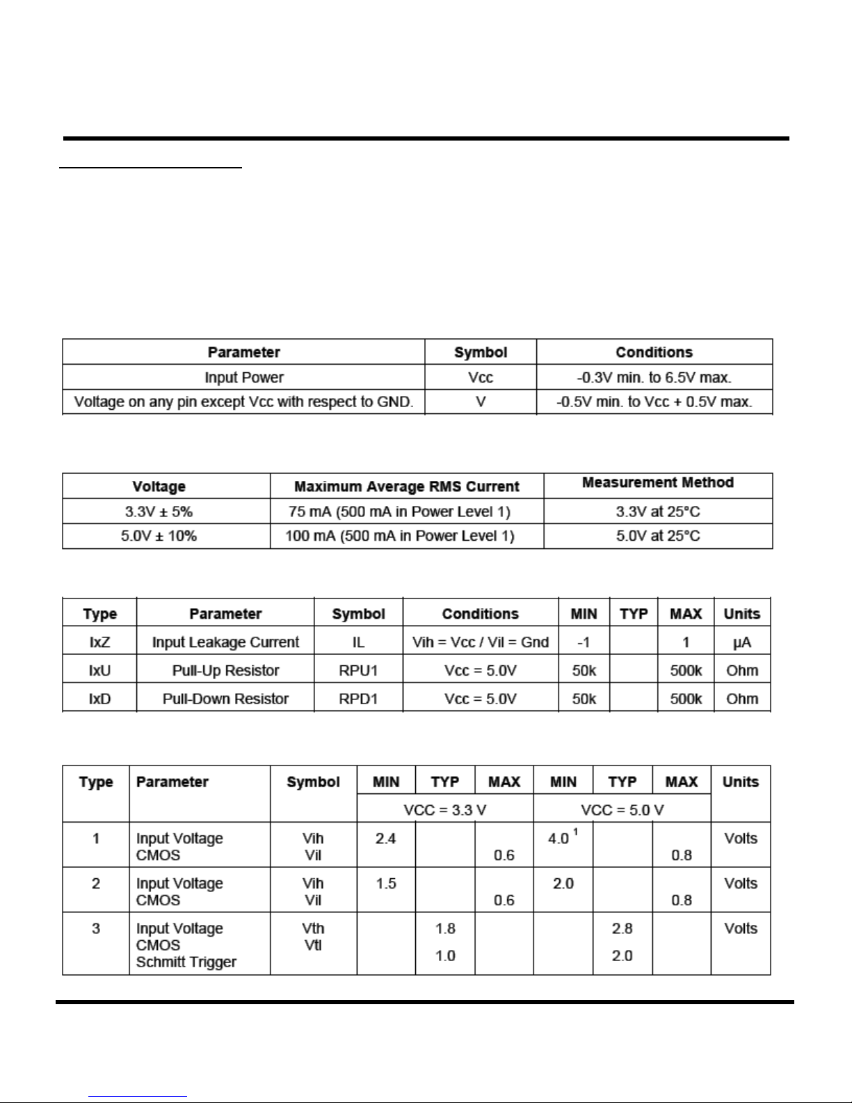
Absolute Maximum Conditions
G
C
F
F
2
2
6
6
6
6
266X CompactFlash Card
Input Power
Input Leakage Current
Input Characteristics
Transcend Information Inc.
11
Page 12
T
S
2
G
~
8
G
C
F
2
6
6
T
S
2
G
~
8
G
C
T
S
2
G
~
8
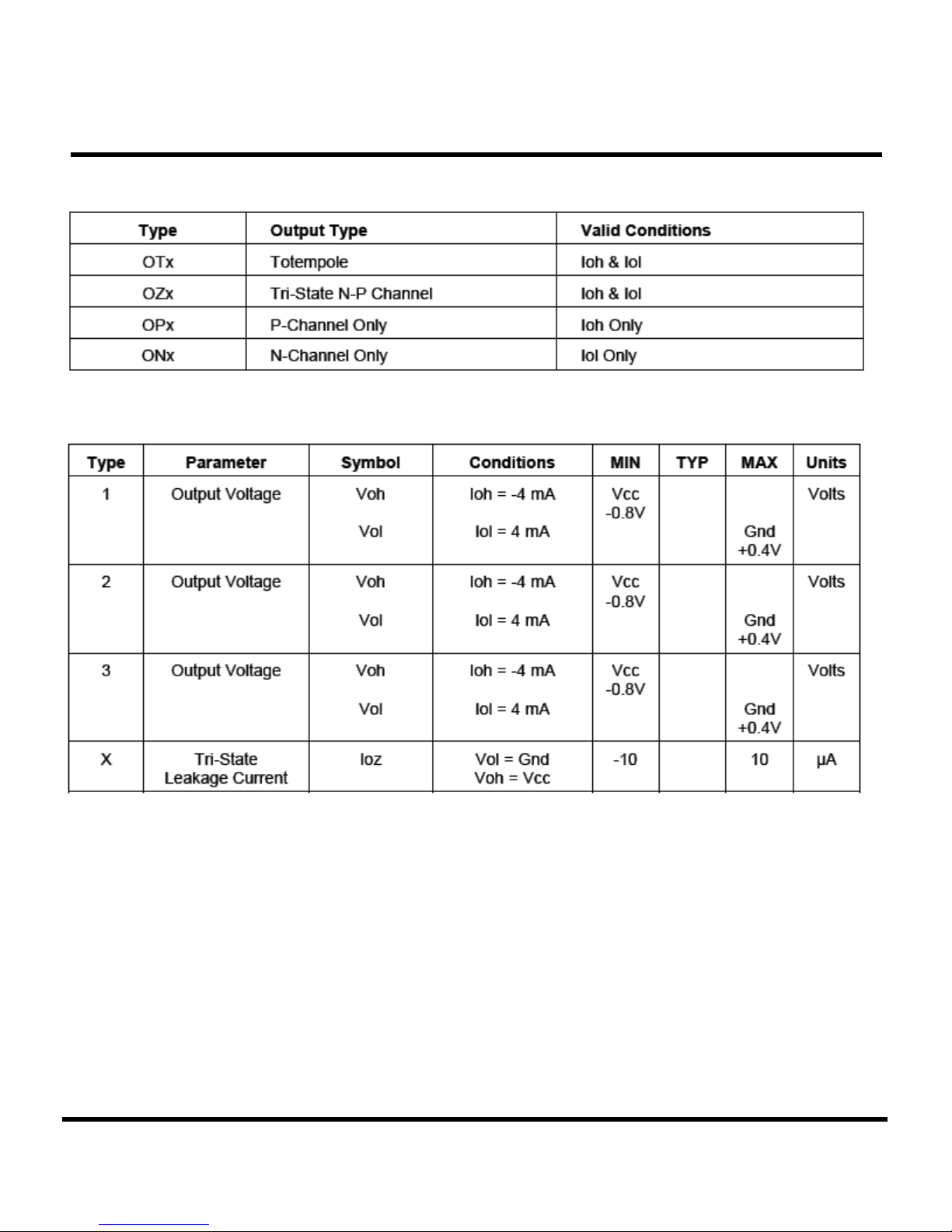
Output Drive Type
G
C
F
F
2
2
6
6
6
6
Output Drive Characteristics
266X CompactFlash Card
Transcend Information Inc.
12
Page 13
T
S
2
G
~
8
G
C
F
T
S
2
G
~
8
G
~
8
G
G
T
S
2
Signal Interface
C
C
F
F
2
2
2
6
6
6
6
6
6
266X CompactFlash Card
Transcend Information Inc.
13
Page 14

T
S
2
G
~
8
G
C
F
2
6
6
T
T
S
S
2
2
G
G
~
~
8
8
G
G
C
C
F
F
2
2
6
6
6
6
266X CompactFlash Card
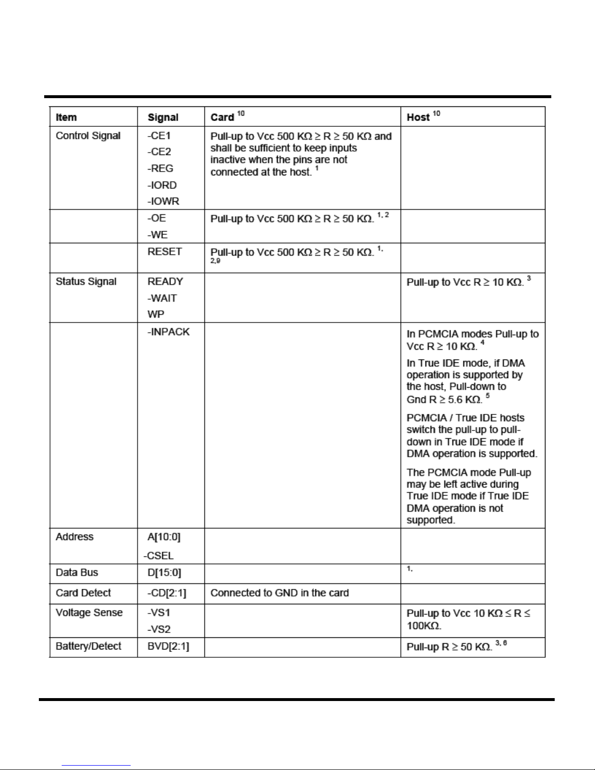
Notes: 1) Control Signals: each card shall present a load to the socket no larger than 50 pF 10 at a DC current of 700 μA low
state and 150 μA high state, including pull-resistor. The socket shall be able to drive at least the following load
10 while meeting all AC timing requirements: (the number of sockets w ired in parallel) multiplied by (50 pF with DC
current 700 μA low state and 150 μA high state per socket).
2) Resistor is optional.
3) Status Signals: the socket shall present a load to the card no larger than 50 pF
state and 100 μA high state, including pull-up resistor. The card shall be able to drive at least the following load
10 while meeting all AC timing requirements: 50 pF at a DC current of 400 μA low state and 100 μA high state.
4) Status Signals: the socket shall present a load to the card no larger than 50 pF
state and 100 μA high state, including pull-up resistor. The card shall be able to drive at least the following load
10 while meeting all AC timing requirements: 50 pF at a DC current of 400 μA low state and 100 μA high state.
5) Status Signals: the socket shall present a load to the card no larger than 50 pF
state and 100 μA high state, including pull-up resistor. The card shall be able to drive at least the following load
10 while meeting all AC timing requirements: 50 pF at a DC current of 400 μA low state and 1100 μA high state.
6) BVD2 was not defined in the JEIDA 3.0 release. Systems fully supporting JEIDA release 3 SRAM cards shall
pull-up pin 45 (BVD2) to avoid sensing their batteries as “Low.”
7) Address Signals: each card shall present a load of no more than 100pF
150μA high state. The host shall be able to drive at least the following load
requirements: (the number of sockets wired in parallel) multiplied by (100pF with DC current 450μA low state
and 150μA high state per socket).
8) Data Signals: the host and each card shall present a load no larger than 50pF
150μA high state. The host and each card shall be able to drive at least the following load
timing requirements: 100pF with DC current 1.6mA low state and 300μA high state. This permits the host to wire
two sockets in parallel without derating the card access speeds.
9) Reset Signal: This signal is pulled up to prevent the input from floating when a CFA to PCMCIA adapter is used in
a PCMCIA revision 1 host. However, to minimize DC current drain through the pull-up resistor in normal
operation the pull-up should be turned off once the Reset signal has been actively driven low by the host.
Consequently, the input is specified as an I2Z because the resistor is not necessarily detectable in the input
current leakage test.
10) Host and card restrictions for CF Advanced Timing Modes and Ultra DMA modes: Additional Requirements for
CF Advanced Timing Modes and Ultra DMA Electrical Requirements for additional required limitations on the
implementation of CF Advanced Timing modes and Ultra DMA modes respectively.
Additional Requirements for CF Advanced Timing Modes
The CF Advanced Timing modes include PCMCIA I/O and Memory modes that are 100ns or faster and True
IDE PIO Modes 5,6 and Multiword DMA Modes 3,4.
When operating in CF Advanced timing modes, the host shall conform to the following requirements:
1) Only one CF device shall be attached to the CF Bus.
2) The host shall not present a load of more than 40pF to the device for all signals, including any cabling.
3) The maximum cable length is 0.15 m (6 in). The cable length is measured from the card connector to the host
controller. 0.46 m (18 in) cables are not supported.
4) The -WAIT and IORDY signals shall be ignored by the host.
Devices supporting CF Advanced timing modes shall also support slower timing modes, to ensure operability with
systems that do not support CF Advanced timing modes
10 at a DC current of 450μA low state and
10 at a DC current of 400 μA low
10 at a DC current of 400 μA low
10 at a DC current of 400 μA low
10 while meeting all AC timing
10 at a DC current of 450μA and
10 while meeting all AC
Transcend Information Inc.
14
Page 15
T
S
2
G
~
8
G
C
F
2
6
6
T
S
2
G
~
8
G
C
T
S
2
G
~
8
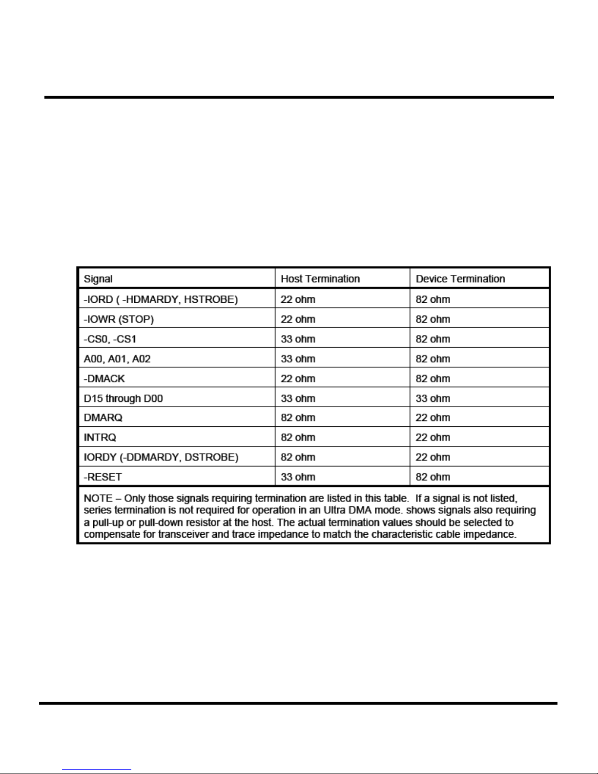
Ultra DMA Electrical Requirements
Host and Card signal capacitance limits for Ultra DMA operation
The host interface signal capacitance at the host connector shall be a maximum of 25 pF for each signal as measured at
1 MHz. The card interface signal capacitance at the card connector shall be a maximum of 20 pF for each signal as
measured at 1 MHz.
Series termination required for Ultra DMA operation
Series termination resistors are required at both the host and the card for operation in any of the Ultra DMA modes. Table
13 describes typical values for series termination at the host and the device.
G
C
F
F
2
2
6
6
6
6
266X CompactFlash Card
Transcend Information Inc.
Table: Typical Series Termination for Ultra DMA
15
Page 16
T
T
T
S
S
S
2
2
2
G
G
G
~
~
~
8
8
8
G
G
G
C
C
C
F
F
F
2
2
2
6
6
6
6
6
6
266X CompactFlash Card
Table: Ultra DMA Termination with Pull-up or Pull down Example
Printed Circuit Board (PCB) Trace Requirements for Ultra DMA
On any PCB for a host or device supporting Ultra DMA:
The longest D[15:00] trace shall be no more than 0.5" longer than either STROBE trace as measured from
the IC pin to the connector.
The shortest D[15:00] trace shall be no more than 0.5" shorter than either STROBE trace as measured from
the IC pin to the connector.
Ultra DMA Mode Cabling Requirement
Operation in Ultra DMA mode requires a crosstalk suppressing cable. The cable shall have a grounded line
between each signal line.
For True IDE mode operation using a cable with IDE (ATA) type 40 pin connectors it is recommended that the
host sense the cable type using the method described in the ANSI INCITS 361-2002 AT Attachment - 6
standard, to prevent use of Ultra DMA with a 40 conductor cable.
Transcend Information Inc.
16
Page 17
T
S
2
G
~
8
G
C
F
2
6
6
T
S
2
G
~
8
G
C
T
S
2
G
~
8
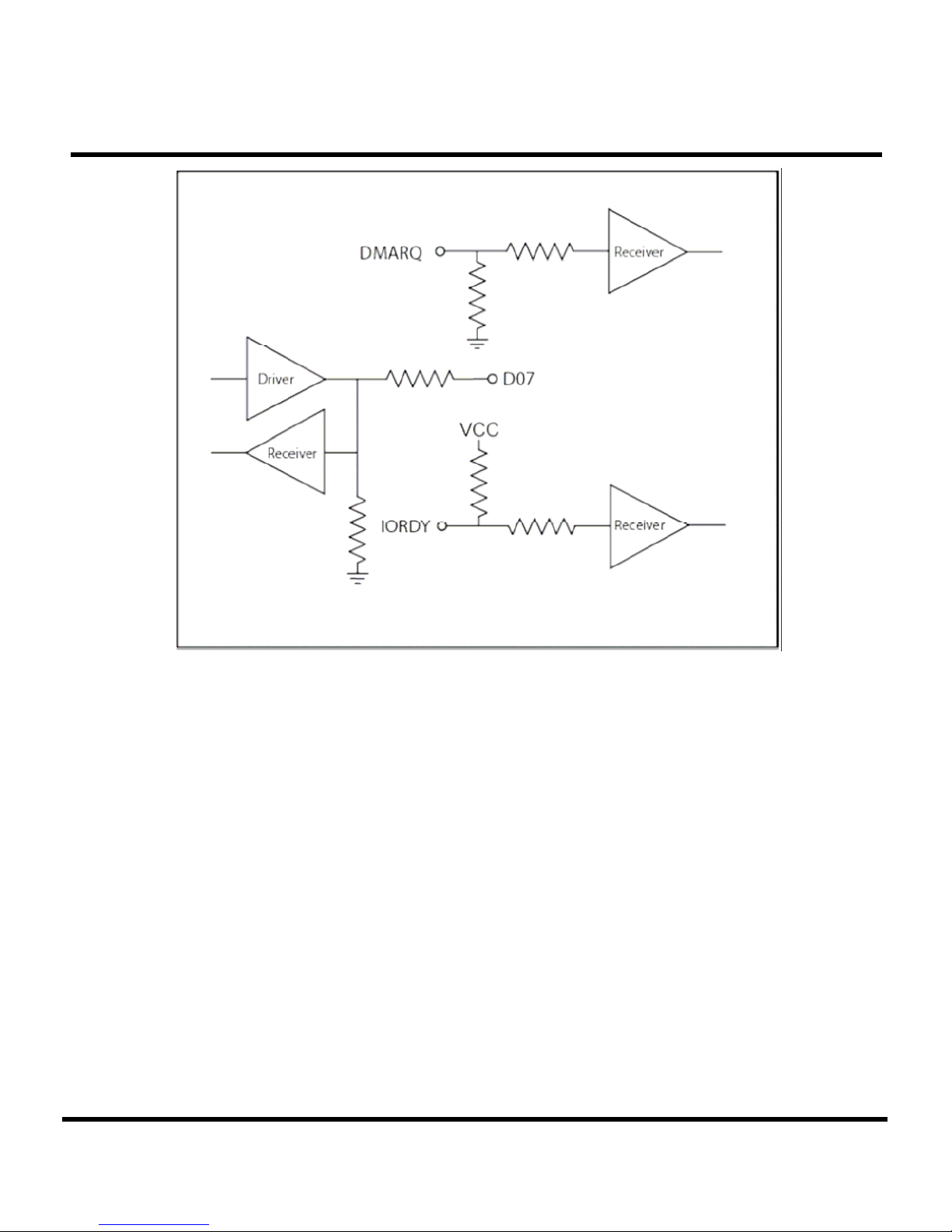
Attribute Memory Read Timing Specification
G
C
F
F
2
2
6
6
6
6
266X CompactFlash Card
Transcend Information Inc.
17
Page 18
T
S
2
G
~
8
G
C
F
2
6
6
T
S
2
G
~
8
G
C
T
S
2
G
~
8
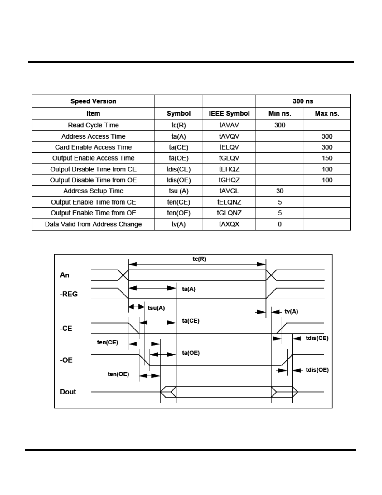
Configuration Register (Attribute Memory) Write Timing Specification
G
C
F
F
2
2
6
6
6
6
266X CompactFlash Card
Transcend Information Inc.
18
Page 19
T
S
2
G
~
8
G
C
F
2
6
6
T
S
2
G
~
8
G
C
T
S
2
G
~
8
Common Memory Read Timing Specification
G
C
F
F
2
2
6
6
6
6
266X CompactFlash Card
Transcend Information Inc.
19
Page 20
T
S
2
G
~
8
G
C
F
2
6
6
2
2
6
6
6
6
T
T
S
S
2
2
G
G
~
~
8
8
G
G
C
C
F
F
Common Memory Write Timing Specification
266X CompactFlash Card
Transcend Information Inc.
20
Page 21
T
S
2
G
~
8
G
C
F
2
6
6
T
S
2
G
~
8
G
C
T
S
2
G
~
8
I/O Input (Read) Timing Specification
G
C
F
F
2
2
6
6
6
6
266X CompactFlash Card
Transcend Information Inc.
21
Page 22
T
T
T
T
T
T
S
S
S
S
S
S
2
2
2
2
2
2
G
G
G
G
G
G
~
~
~
~
~
~
8
8
8
8
8
8
G
G
G
G
G
G
C
C
C
C
C
C
F
F
F
F
F
F
2
2
2
2
2
2
6
6
6
6
6
6
6
6
6
6
6
6
266X CompactFlash Card
266X CompactFlash Card
Transcend Information Inc.
Transcend Information Inc.
22
22
Page 23
T
S
2
G
~
8
G
C
F
2
6
6
T
S
2
G
~
8
G
C
T
S
2
G
~
8
I/O Output (Write) Timing Specification
G
C
F
F
2
2
6
6
6
6
266X CompactFlash Card
Transcend Information Inc.
23
Page 24
T
T
T
T
T
T
S
S
S
S
S
S
2
2
2
2
2
2
G
G
~
~
8
8
G
G
C
C
F
F
2
2
6
6
6
6
G
G
G
G
~
~
~
~
8
8
8
8
G
G
G
G
C
C
C
C
F
F
F
F
2
2
2
2
6
6
6
6
6
6
6
6
266X CompactFlash Card
266X CompactFlash Card
Transcend Information Inc.
Transcend Information Inc.
24
24
Page 25

T
S
2
G
~
8
G
C
F
2
6
6
T
S
2
G
~
8
G
C
T
S
2
G
~
8
True IDE PIO Mode Read/Write Timing Specification
G
C
F
F
2
2
6
6
6
6
266X CompactFlash Card
Transcend Information Inc.
25
Page 26

T
T
T
S
S
S
2
2
2
G
G
G
~
~
~
8
8
8
G
G
G
C
C
C
F
F
F
2
2
2
6
6
6
6
6
6
266X CompactFlash Card
Transcend Information Inc.
26
Page 27

T
S
2
G
~
8
G
C
F
2
6
6
T
S
2
G
~
8
G
C
T
S
2
G
~
8
True IDE Ultra DMA Mode Read/Write Timing Specification
G
C
F
F
2
2
6
6
6
6
Table: Ultra DMA Data Burst Timing
266X CompactFlash Card
Transcend Information Inc.
27
Page 28

T
T
S
2
G
~
8
G
C
F
2
6
6
S
2
G
~
8
G
C
T
S
2
G
~
8
Notes: 1) All timing measurement switching points (low to high and high to low) shall be taken at 1.5 V.
F
G
C
F
2) All signal transitions for a timing parameter shall be measured at the connector specified in the
measurement location column. For example, in the case of tRFS, both STROBE and –DMARDY
transitions are measured at the sender connector.
3) The parameter tCYC shall be measured at the recipient’s connector farthest from the sender.
4)The parameter tLI shall be measured at the connector of the sender or recipient that is
responding to an incoming transition from the recipient or sender respectively. Both the incoming
signal and the outgoing response shall be measured at the same connector.
5)The parameter tAZ shall be measured at the connector of the sender or recipient that is driving
the bus but must release the bus the allow for a bus turnaround.
2
2
6
6
6
6
266X CompactFlash Card
Transcend Information Inc.
28
Page 29

T
T
T
S
S
S
2
2
2
G
G
G
~
~
~
8
8
8
G
G
G
C
C
C
F
F
F
2
2
2
6
6
6
6
6
6
266X CompactFlash Card
Transcend Information Inc.
29
Page 30

T
T
S
2
G
~
8
G
C
F
2
6
6
S
2
G
~
8
G
C
T
S
2
G
~
8
Notes: 1) The parameters tUI, tMLI : (Ultra DMA Data-In Burst Device Termination Timing and Ultra DMA
F
G
C
F
Data-In Burst Host Termination Timing), and tLI indicate sender-to-recipient or recipient-to-sender
interlocks, i.e., one agent (either sender or recipient) is waiting for the other agent to respond with a
signal before proceeding. tUI is an unlimited interlock that has no maximum time value. tMLI is a
limited time-out that has a defined minimum. tLI is a limited time-out that has a defined maximum.
2) 80-conductor cabling shall be required in order to meet setup (tDS, tCS) and hold (tDH, tCH) times
in modes greater than 2.
3) Timing for tDVS, tDVH, tCVS and tCVH shall be met for lumped capacitive loads of 15 and 40 pF
at the connector where the Data and STROBE signals have the same capacitive load value. Due to
reflections on the cable, these timing measurements are not valid in a normally functioning system.
4)For all modes the parameter tZIORDY may be greater than tENV due to the fact that the host has
a pull-up on IORDY- giving it a known state when released.
5)The parameters tDS, and tDH for mode 5 are defined for a recipient at the end of the cable only in
a configuration with a single device located at the end of the cable. This could result in the minimum
values for tDS and tDH for mode 5 at the middle connector being 3.0 and 3.9 ns respectively.
2
2
6
6
6
6
266X CompactFlash Card
Notes: 1) All timing measurement switching points(low to high and high to low) shall be taken at 1.5 V.
2) The correct data value shall be captured by the recipient given input data with a slew rate of 0.4
V/ns rising and falling and the input STROBE with a slew rate of 0.4 V/ns rising and falling at tDSIC
and tDHIC timing (as measured through 1.5 V).
3) The parameters tDVSIC and tDVHIC shall be met for lumped capacitive loads of 15 and 40 pF at
the IC where all signals have the same capacitive load value. Noise that may couple onto the output
signals from external sources has not been included in these values.
Transcend Information Inc.
30
Page 31
T
T
S
2
G
~
8
G
C
F
2
6
6
S
2
G
~
8
G
C
T
S
2
G
~
8
Note: 1) The sender shall be tested while driving an 18 inch long, 80 conductor cable with PVC insulation
F
G
C
F
material. The signal under test shall be cut at a test point so that it has not trace, cable or recipient
loading after the test point. All other signals should remain connected through to the recipient. The
test point may be located at any point between the sender’s series termination resistor and one half
inch or less of conductor exiting the connector. If the test point is on a cable conductor rather than the
PCB, an adjacent ground conductor shall also be cut within one half inch of the connector.
The test load and test points should then be soldered directly to the exposed source side connectors.
The test loads consist of a 15 pF or a 40 pF, 5%, 0.08 inch by 0.05 inch surface mount or smaller size
capacitor from the test point to ground. Slew rates shall be met for both capacitor values.
Measurements shall be taken at the test point using a <1 pF, >100 Kohm, 1 Ghz or faster probe and
a 500 MHz or faster oscilloscope. The average rate shall be measured from 20% to 80% of the settled
VOH level with data transitions at least 120 nsec apart. The settled VOH level shall be measured as
the average output high level under the defined testing conditions from 100 nsec after 80% of a rising
edge until 20% of the subsequent falling edge.
2
2
6
6
6
6
266X CompactFlash Card
Transcend Information Inc.
31
Page 32

T
S
2
G
~
8
G
C
F
2
6
6
T
S
2
G
~
8
G
C
T
S
2
G
~
8
Card Configuration
The CompactFlash Storage Cards and CF+ Cards are identified by appropriate information in the Card
Information Structure (CIS). The following configuration registers are used to coordinate the I/O spaces and the
Interrupt level of cards that are located in the system. In addition, these registers provide a method for accessing
status information about the CompactFlash Storage Card or CF+ Card that may be used to arbitrate between
multiple interrupt sources on the same interrupt level or to replace status information that appears on dedicated
pins in memory cards that have alternate use in I/O cards.
Single Function CF+ Cards
Single function CF+ Cards shall have a single configuration tuple describing a single set of Function
Configuration registers
Multiple Function CF+ Cards
G
C
F
F
2
6
6
2
6
6
Table: CompactFlash Storage Card Registers and Memory Space Decoding
266X CompactFlash Card
Table: CompactFlash Storage Card Configuration Registers Decoding
Transcend Information Inc.
32
Page 33

T
T
T
S
S
S
2
2
2
G
G
G
~
~
~
8
8
8
G
G
G
C
C
C
F
F
F
2
2
2
6
6
6
6
6
6
Table: CF+ Card Register and Memory Space Decoding
266X CompactFlash Card
Transcend Information Inc.
Table: CF+ Card Configuration Registers Decoding
33
Page 34

T
S
2
G
~
8
G
C
F
2
6
6
T
S
2
G
~
8
G
C
T
S
2
G
~
8
Attribute Memory Function
Attribute memory is a space where CompactFlash Storage Card and CF+ Card identification and
configuration information are stored, and is limited to 8 bit wide accesses only at even addresses. The card
configuration registers are also located here. For CompactFlash Storage Cards, the base address of the ard
configuration registers is 200h. For CF+ cards, the base address of the card configuration registers is
determined by the Configuration tuple (CISTPL_CONFIG).
G
C
F
F
2
2
6
6
6
6
Table 31: Attribute Memory Function
266X CompactFlash Card
Transcend Information Inc.
34
Page 35

T
S
2
G
~
8
G
C
F
2
6
6
T
S
2
G
~
8
G
C
T
S
2
G
~
8
Configuration Option Register (Base + 00h in Attribute Memory)
G
C
F
F
2
2
6
6
6
6
266X CompactFlash Card
Transcend Information Inc.
35
Page 36

T
S
2
G
~
8
G
C
F
2
6
6
T
S
2
G
~
8
G
C
T
S
2
G
~
8
Card Configuration and Status Register (Base + 02h in Attribute Memory)
G
C
F
F
2
2
6
6
6
6
266X CompactFlash Card
Transcend Information Inc.
36
Page 37

T
S
2
G
~
8
G
C
F
2
6
6
T
S
2
G
~
8
G
C
T
S
2
G
~
8
Pin Replacement Register (Base + 04h in Attribute Memory)
G
C
F
F
2
2
6
6
6
6
266X CompactFlash Card
Transcend Information Inc.
37
Page 38

T
S
2
G
~
8
G
C
F
2
6
6
T
S
2
G
~
8
G
C
T
S
2
G
~
8
Socket and Copy Register (Base + 06h in Attribute Memory)
G
C
F
F
2
2
6
6
6
6
266X CompactFlash Card
Transcend Information Inc.
38
Page 39

T
S
2
G
~
8
G
C
F
2
6
6
T
S
2
G
~
8
G
C
T
S
2
G
~
8
I/O Transfer Function
The I/O transfer to or from the CompactFlash Storage or CF+ Card can be either 8 or 16 bits. When a 16 bit
accessible port is addressed, the signal -IOIS16 is asserted by the CompactFlash Storage or CF+ Card.
Otherwise, the -IOIS16 signal is de-asserted. When a 16 bit transfer is attempted, and the -IOIS16 signal is
not asserted by the CompactFlash Storage or CF+ Card, the system shall generate a pair of 8 bit references
to access the word‘s even byte and odd byte. The CompactFlash Storage Card permits both 8 and 16 bit
accesses to all of its I/O addresses, so -IOIS16 is asserted for all addresses to which the CompactFlash
Storage responds. CF+ cards may or may not allow 16 bit register accesses and thus shall assert -IOIS16 as
required. The CompactFlash Storage and CF+ Card may request the host to extend the length of an input
cycle until data is ready by asserting the -WAIT signal at the start of the cycle.
G
C
F
F
2
2
6
6
6
6
266X CompactFlash Card
Table : PCMCIA Mode I/O Function
Transcend Information Inc.
39
Page 40

T
S
2
G
~
8
G
C
F
2
6
6
T
S
2
G
~
8
G
C
T
S
2
G
~
8
Common Memory Transfer Function
G
C
F
F
2
2
6
6
6
6
266X CompactFlash Card
The Common Memory transfer to or from the CompactFlash Storage or CF+ Card can be either 8 or 16 bits.
Table: Common Memory Function
Transcend Information Inc.
40
Page 41

T
S
2
G
~
8
G
C
F
2
6
6
T
S
2
G
~
8
G
C
T
S
2
G
~
8
True IDE Mode I/O Transfer Function
The CompactFlash Storage Card and CF+ Card can be configured in a True IDE Mode of operation. The
CompactFlash Storage Card is configured in this mode only when the -OE input signal is grounded by the host
during the power off to power on cycle. Optionally, CompactFlash Storage Cards and CF+ Cards may support the
following optional detection methods:
1. The card is permitted to monitor the –OE (-ATA SEL) signal at any time(s) and switch to PCMCIA mode upon
detecting a high level on the pin.
2. The card is permitted to re-arbitrate the interface mode determination following a transition of the (-)RESET pin.
3. The card is permitted to monitor the –OE (-ATA SEL) signal at any time(s) and switch to True IDE mode upon
detection of a continuous low level on pin for an extended period of time.
Table: True IDE Mode I/O Function defines the function of the operations for the True IDE Mode.
G
C
F
F
2
2
6
6
6
6
266X CompactFlash Card
Transcend Information Inc.
41
Page 42

T
S
2
G
~
8
G
C
F
2
6
6
T
S
2
G
~
8
G
C
T
S
2
G
~
8
Metaformat Overview
The goal of the Metaformat is to describe the requirements and capabilities of the CompactFlash Storage Card
and CF+ Card as thoroughly as possible. This includes describing the power requirements, IO requirements,
memory requirements, manufacturer information and details about the services provided.
G
C
F
F
2
2
6
6
6
6
266X CompactFlash Card
Table: Sample Device Info Tuple Information for Extended Speeds
Note: The value “1” defined for D3 of the N+0 words indicates that no write-protect switch controls writing the ATA
registers. The value “0” defined for D7 in the N+2 words indicates that there is not more than a single speed
extension byte.
Transcend Information Inc.
42
Page 43

T
S
2
G
~
8
G
C
F
2
6
6
T
S
2
G
~
8
G
C
T
S
2
G
~
8
CF-ATA Drive Register Set Definition and Protocol
The CompactFlash Storage Card can be configured as a high performance I/O device through:
a) The standard PC-AT disk I/O address spaces 1F0h-1F7h, 3F6h-3F7h (primary) or 170h- 177h, 376h-377h
(secondary) with IRQ 14 (or other available IRQ).
b) Any system decoded 16 byte I/O block using any available IRQ.
c) Memory space.
The communication to or from the CompactFlash Storage Card is done using the Task File registers, which
provide all the necessary registers for control and status information related to the storage medium. The PCMCIA
interface connects peripherals to the host using four register mapping methods. Table 39 is a detailed description
of these methods:
G
C
F
F
2
2
6
6
6
6
266X CompactFlash Card
Transcend Information Inc.
43
Page 44

T
S
2
G
~
8
G
C
F
2
6
6
T
S
2
G
~
8
G
C
T
S
2
G
~
8
I/O Primary and Secondary Address Configurations
G
C
F
F
2
2
6
6
6
6
Table: Primary and Secondary I/O Decoding
266X CompactFlash Card
Transcend Information Inc.
44
Page 45
T
S
2
G
~
8
G
C
F
2
6
6
T
S
2
G
~
8
G
C
T
S
2
G
~
8
Contiguous I/O Mapped Addressing
When the system decodes a contiguous block of I/O registers to select the CompactFlash Storage Card, the
registers are accessed in the block of I/O space decoded by the system as follows:
G
C
F
F
2
2
6
6
6
6
Table: Contiguous I/O Decoding
266X CompactFlash Card
Transcend Information Inc.
45
Page 46
T
S
2
G
~
8
G
C
F
2
6
6
T
S
2
G
~
8
G
C
T
S
2
G
~
8
Memory Mapped Addressing
When the CompactFlash Storage Card registers are accessed via memory references, the registers appear in the
common memory space window: 0-2K bytes as follows:
G
C
F
F
2
2
6
6
6
6
266X CompactFlash Card
True IDE Mode Addressing
When the CompactFlash Storage Card or CF+ Card is configured in the True IDE Mode, the I/O decoding is as
follows:
Transcend Information Inc.
46
Page 47
T
S
2
G
~
8
G
C
F
2
6
6
T
S
2
G
~
8
G
C
T
S
2
G
~
8
CF-ATA Registers
The following section describes the hardware registers used by the host software to issue commands to the
CompactFlash device. These registers are often collectively referred to as the “task file.”
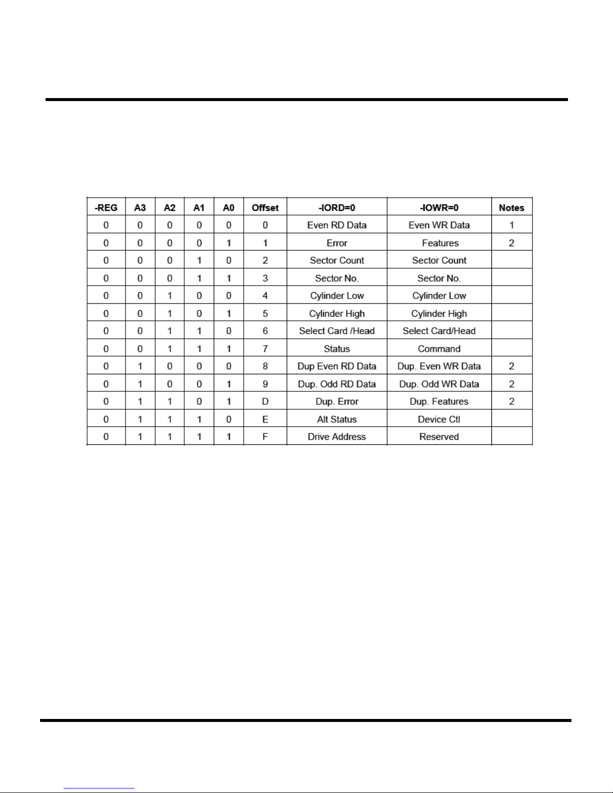
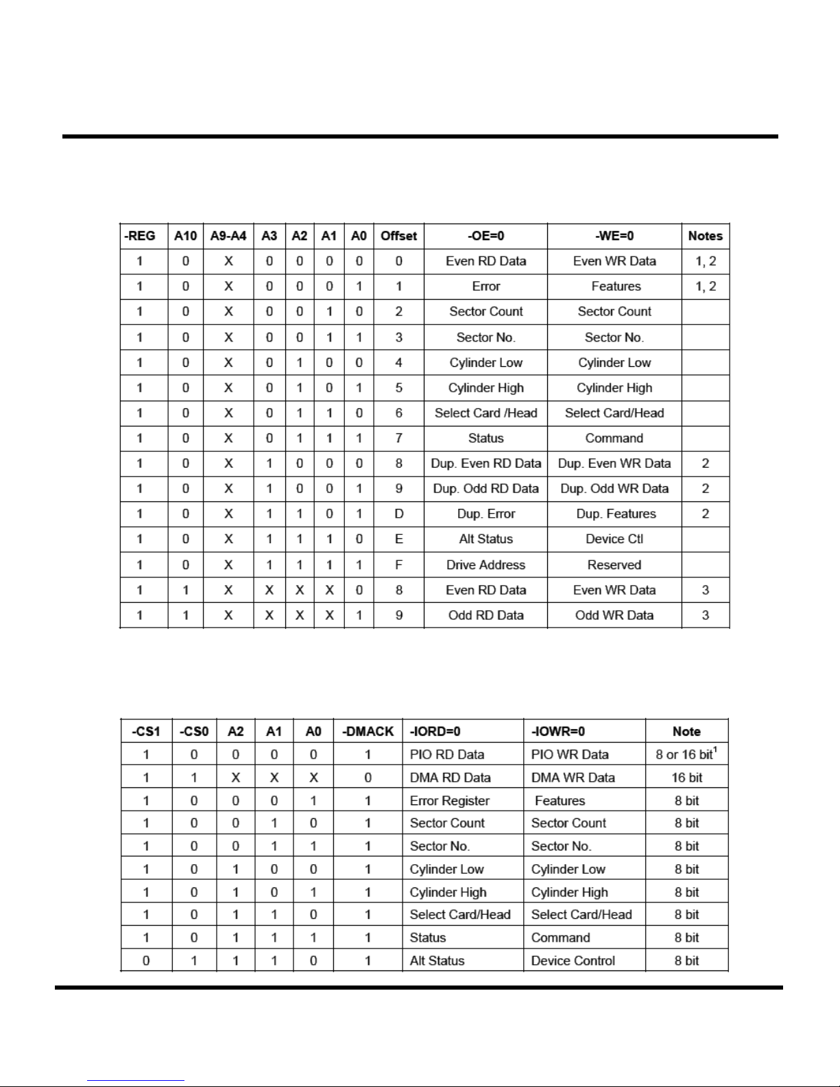
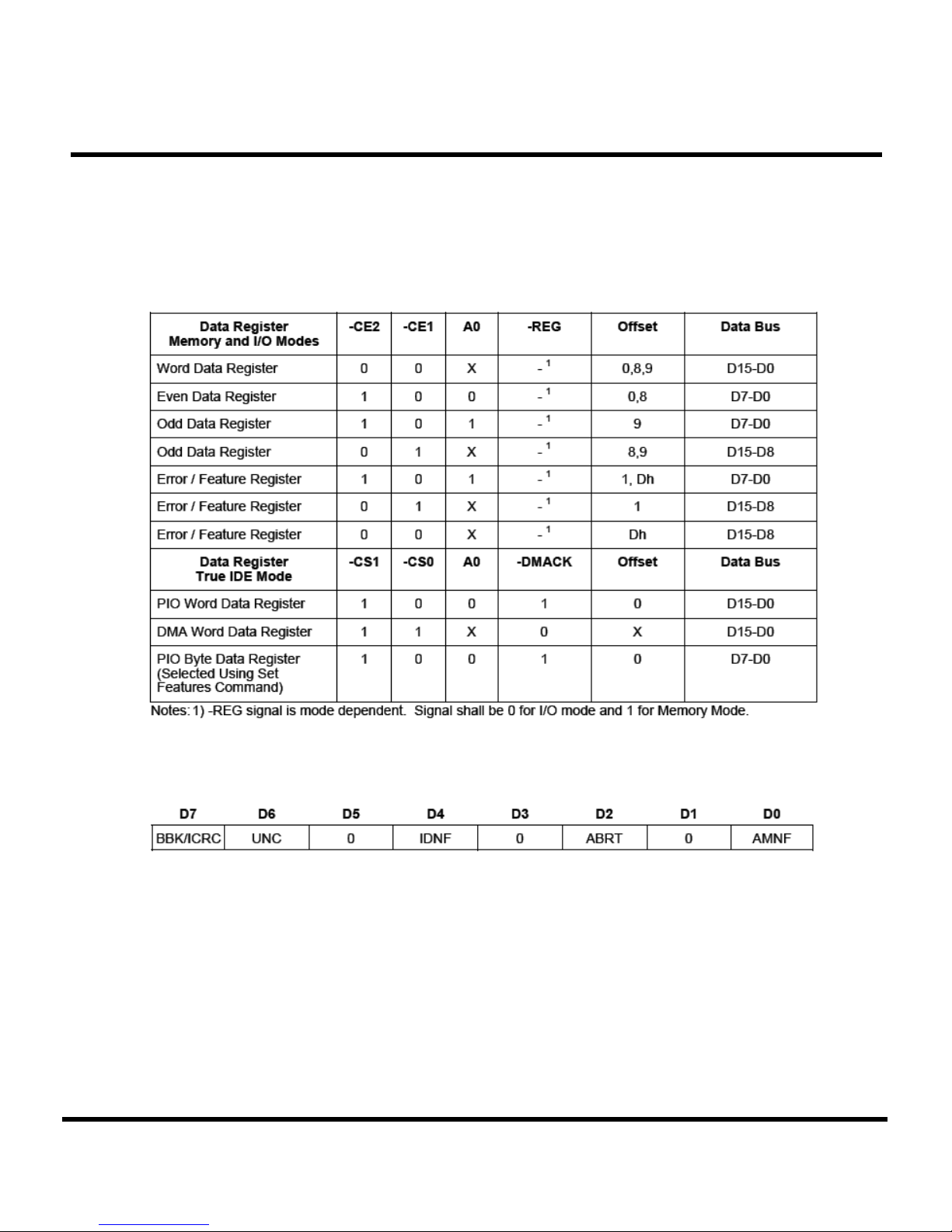
Data Register (Address - 1F0h[170h];Offset 0,8,9)
The Data Register is a 16 bit register, and it is used to transfer data blocks between the CompactFlash
Storage Card data buffer and the Host. This register overlaps the Error Register.
G
C
F
F
2
2
6
6
6
6
266X CompactFlash Card
Error Register (Address - 1F1h[171h]; Offset 1, 0Dh Read Only)
This register contains additional information about the source of an error when an error is indicated in bit 0
of the Status register.
This register is also accessed in PC Card Modes on data bits D15-D8 during a read operation to offset 0
with -CE2 low and -CE1 high.
Bit 7 (BBK/ICRC): this bit is set when a Bad Block is detected. This bit is also set when an interface CRC
error is detected in True IDE Ultra DMA modes of operation.
Bit 6 (UNC): this bit is set when an Uncorrectable Error is encountered.
Bit 5: this bit is 0.
Bit 4 (IDNF): the requested sector ID is in error or cannot be found.
Bit 3: this bit is 0.
Bit 2 (Abort) This bit is set if the command has been aborted because of a CompactFlash Storage Card
status condition: (Not Ready, Write Fault, etc.) or when an invalid command has been issued.
Bit 1 This bit is 0.
Bit 0 (AMNF) This bit is set in case of a general error.
Transcend Information Inc.
47
Page 48

T
S
2
G
~
8
G
C
F
2
6
6
T
S
2
G
~
8
G
C
T
S
2
G
~
8
Feature Register (Address - 1F1h[171h]; Offset 1, 0Dh Write Only)
This register provides information regarding features of the CompactFlash Storage Card that the host can
utilize. This register is also accessed in PC Card modes on data bits D15-D8 during a write operation to
Offset 0 with -CE2 low and -CE1 high.
Sector Count Register (Address - 1F2h[172h]; Offset 2)
This register contains the numbers of sectors of data requested to be transferred on a read or write
operation between the host and the CompactFlash Storage Card. If the value in this register is zero, a count
of 256 sectors is specified. If the command was successful, this register is zero at command completion. If
not successfully completed, the register contains the number of sectors that need to be transferred in order
to complete the request.
Sector Number (LBA 7-0) Register (Address - 1F3h[173h]; Offset 3)
This register contains the starting sector number or bits 7-0 of the Logical Block Address (LBA) for any
CompactFlash Storage Card data access for the subsequent command.
6.1.5.5 Cylinder Low (LBA 15-8) Register (Address - 1F4h[174h]; Offset 4)
This register contains the low order 8 bits of the starting cylinder address or bits 15-8 of the Logical Block
Address.
Cylinder High (LBA 23-16) Register (Address - 1F5h[175h]; Offset 5)
This register contains the high order bits of the starting cylinder address or bits 23-16 of the Logical Block
Address.
Drive/Head (LBA 27-24) Register (Address 1F6h[176h]; Offset 6)
The Drive/Head register is used to select the drive and head. It is also used to select LBA addressing
instead of cylinder/head/sector addressing.
Bit 7: this bit is specified as 1 for backward compatibility reasons. It is intended that this bit will become
Bit 6: LBA is a flag to select either Cylinder/Head/Sector (CHS) or Logical Block Address Mode (LBA).
Bit 5: this bit is specified as 1 for backward compatibility reasons. It is intended that this bit will become
Bit 4 (DRV): DRV is the drive number. When DRV=0, drive (card) 0 is selected. When DRV=1, drive (card)
F
G
C
F
obsolete in a future revision of the specification. This bit is ignored by some controllers in some
commands.
When LBA=0, Cylinder/Head/Sector mode is selected. When LBA=1, Logical Block Address is
selected. In Logical Block Mode, the Logical Block Address is interpreted as follows:
LBA7-LBA0: Sector Number Register D7-D0.
LBA15-LBA8: Cylinder Low Register D7-D0.
LBA23-LBA16: Cylinder High Register D7-D0.
LBA27-LBA24: Drive/Head Register bits HS3-HS0.
obsolete in a future revisions of the specification. This bit is ignored by some controllers in some
commands.
1 is selected. Setting this bit to 1 is obsolete in PCMCIA modes of operation. If the obsolete
functionality is support by a CF Storage Card, the CompactFlash Storage Card is set to be Card 0 or 1
using the copy field (Drive #) of the PCMCIA Socket & Copy configuration register.
2
2
6
6
6
6
266X CompactFlash Card
Transcend Information Inc.
48
Page 49

T
S
2
G
~
8
G
C
F
2
6
6
T
S
2
G
~
8
G
C
T
S
2
G
~
8
Bit 3 (HS3): when operating in the Cylinder, Head, Sector mode, this is bit 3 of the head number. It is Bit
Bit 2 (HS2): when operating in the Cylinder, Head, Sector mode, this is bit 2 of the head number. It is Bit
Bit 1 (HS1): when operating in the Cylinder, Head, Sector mode, this is bit 1 of the head number. It is Bit
Bit 0 (HS0): when operating in the Cylinder, Head, Sector mode, this is bit 0 of the head number. It is Bit
Status & Alternate Status Registers (Address 1F7h[177h]&3F6h[376h]; Offsets 7 & Eh)
These registers return the CompactFlash Storage Card status when read by the host. Reading
the Status register does clear a pending interrupt while reading the Auxiliary Status register does
not. The status bits are described as follows:
Bit 7 (BUSY): the busy bit is set when the CompactFlash Storage Card has access to the command buffer
Bit 6 (RDY): RDY indicates whether the device is capable of performing CompactFlash Storage Card
Bit 5 (DWF): This bit, if set, indicates a write fault has occurred.
Bit 4 (DSC): This bit is set when the CompactFlash Storage Card is ready.
Bit 3 (DRQ): The Data Request is set when the CompactFlash Storage Card requires that information be
Bit 2 (CORR): This bit is set when a Correctable data error has been encountered and the data has been
Bit 1 (IDX): This bit is always set to 0.
Bit 0 (ERR): This bit is set when the previous command has ended in some type of error. The bits in the
F
G
C
F
27 in the Logical Block Address mode.
26 in the Logical Block Address mode.
25 in the Logical Block Address mode.
24 in the Logical Block Address mode.
and registers and the host is locked out from accessing the command register and buffer. No other bits
in this register are valid when this bit is set to a 1. During the data transfer of DMA commands, the
Card shall not assert DMARQ unless either the BUSY bit, the DRQ bit, or both are set to one.
operations. This bit is cleared at power up and remains cleared until the CompactFlash Storage Card
is ready to accept a command.
transferred either to or from the host through the Data register. During the data transfer of DMA
commands, the Card shall not assert DMARQ unless either the BUSY bit, the DRQ bit, or both are set
to one.
corrected. This condition does not terminate a multi-sector read operation.
Error register contain additional information describing the error. It is recommended that media access
commands (such as Read Sectors and Write Sectors) that end with an error condition should have the
address of the first sector in error in the command block registers.
2
2
6
6
6
6
266X CompactFlash Card
Transcend Information Inc.
49
Page 50

T
S
2
G
~
8
G
C
F
2
6
6
T
S
2
G
~
8
G
C
T
S
2
G
~
8
Device Control Register (Address - 3F6h[376h]; Offset Eh)
This register is used to control the CompactFlash Storage Card interrupt request and to issue an ATA soft
reset to the card. This register can be written even if the device is BUSY. The bits are defined as follows:
Bit 7: this bit is ignored by the CompactFlash Storage Card. The host software should set this bit to 0.
Bit 6: this bit is ignored by the CompactFlash Storage Card. The host software should set this bit to 0.
Bit 5: this bit is ignored by the CompactFlash Storage Card. The host software should set this bit to 0.
Bit 4: this bit is ignored by the CompactFlash Storage Card. The host software should set this bit to 0.
Bit 3: this bit is ignored by the CompactFlash Storage Card. The host software should set this bit to 0.
Bit 2 (SW Rst): this bit is set to 1 in order to force the CompactFlash Storage Card to perform an AT Disk
Bit 1 (-IEn): the Interrupt Enable bit enables interrupts when the bit is 0. When the bit is 1, interrupts from
Bit 0: this bit is ignored by the CompactFlash Storage Card.
F
G
C
F
controller Soft Reset operation. This does not change the PCMCIA Card Configuration Registers as a
hardware Reset does. The Card remains in Reset until this bit is reset to ‘0.’
the CompactFlash Storage Card are disabled. This bit also controls the Int bit in the Configuration and
Status Register. This bit is set to 0 at power on and Reset.
2
2
6
6
6
6
266X CompactFlash Card
Transcend Information Inc.
50
Page 51

T
S
2
G
~
8
G
C
F
2
6
6
T
S
2
G
~
8
G
C
T
S
2
G
~
8
Card (Drive) Address Register (Address 3F7h[377h]; Offset Fh)
This register is provided for compatibility with the AT disk drive interface. It is recommended that this
register not be mapped into the host’s I/O space because of potential conflicts on Bit 7.
Bit 7: this bit is unknown.
Bit 6 (-WTG): this bit is 0 when a write operation is in progress; otherwise, it is 1.
Bit 5 (-HS3): this bit is the negation of bit 3 in the Drive/Head register.
Bit 4 (-HS2): this bit is the negation of bit 2 in the Drive/Head register.
Bit 3 (-HS1): this bit is the negation of bit 1 in the Drive/Head register.
Bit 2 (-HS0): this bit is the negation of bit 0 in the Drive/Head register.
Bit 1 (-nDS1): this bit is 0 when drive 1 is active and selected.
Bit 0 (-nDS0): this bit is 0 when the drive 0 is active and selected.
F
G
C
F
Implementation Note:
Conflicts may occur on the host data bus when this bit is provided by a Floppy Disk Controller
operating at the same addresses as the CompactFlash Storage Card. Following are some possible
solutions to this problem for the PCMCIA implementation:
1) Locate the CompactFlash Storage Card at a non-conflicting address, i.e. Secondary address
(377) or in an independently decoded Address Space when a Floppy Disk Controller is located at
the Primary addresses.
2) Do not install a Floppy and a CompactFlash Storage Card in the system at the same time.
3) Implement a socket adapter that can be programmed to (conditionally) tri-state D7 of I/0 address
3F7h/377h when a CompactFlash Storage Card is installed and conversely to tristate D6-D0 of
I/O address 3F7h/377h when a floppy controller is installed.
4) Do not use the CompactFlash Storage Card’s Drive Address register. This may be accomplished
by either a) If possible, program the host adapter to enable only I/O addresses 1F0h-1F7h, 3F6h
(or 170h-177h, 176h) to the CompactFlash Storage Card or b) if provided use an additional
Primary / Secondary configuration in the CompactFlash Storage Card which does not respond to
accesses to I/O locations 3F7h and 377h. With either of these implementations, the host
software shall not attempt to use information in the Drive Address Register.
2
2
6
6
6
6
266X CompactFlash Card
Transcend Information Inc.
51
Page 52

T
S
2
G
~
8
G
C
F
2
6
6
T
S
2
G
~
8
G
C
T
S
2
G
~
8
CF-ATA Command Set
CF-ATA Command Set summarizes the CF-ATA command set with the paragraphs that follow describing the
individual commands and the task file for each.
G
C
F
F
2
2
6
6
6
6
266X CompactFlash Card
Transcend Information Inc.
52
Page 53

T
S
2
G
~
8
G
C
F
2
6
6
T
S
2
G
~
8
G
C
T
S
2
G
~
8
Check Power Mode - 98h or E5h
If the CompactFlash Storage Card is in, going to, or recovering from the sleep mode, the CompactFlash Storage
Card sets BSY, sets the Sector Count Register to 00h, clears BSY and generates an interrupt.
If the CompactFlash Storage Card is in Idle mode, the CompactFlash Storage Card sets BSY, sets the Sector
Count Register to FFh, clears BSY and generates an interrupt.
F
G
C
F
Definitions:
FR = Features Register
SC = Sector Count RegisterS
SN = Sector Number Register
CY = Cylinder Registers
DH = Card/Drive/Head Register
LBA = Logical Block Address Mode Supported (see command descriptions for use).
Y - The register contains a valid parameter for this command. For the Drive/Head Register Y means
2
6
6
2
6
6
both the CompactFlash Storage Card and head parameters are used; D - only the
CompactFlash Storage Card parameter is valid and not the head parameter; C – The register
contains command specific data (see command descriptions for use).
266X CompactFlash Card
Transcend Information Inc.
53
Page 54

T
S
2
G
~
8
G
C
F
2
6
6
T
S
2
G
~
8
G
C
T
S
2
G
~
8
Execute Drive Diagnostic - 90h
When the diagnostic command is issued in a PCMCIA configuration mode, this command runs only on the
CompactFlash Storage Card that is addressed by the Drive/Head register. This is because PCMCIA card
interface does not allows for direct inter-drive communication (such as the ATA PDIAG and DASP signals). When
the diagnostic command is issued in the True IDE Mode, the Drive bit is ignored and the diagnostic command is
executed by both the Master and the Slave with the Master responding with status for both devices.
Diagnostic Codes are returned in the Error Register at the end of the command.
Erase Sector(s) - C0h
This command is used to pre-erase and condition data sectors in advance of a Write without Erase or Write
Multiple without Erase command. There is no data transfer associated with this command but a Write Fault error
status can occur.
G
C
F
F
2
2
6
6
6
6
266X CompactFlash Card
Transcend Information Inc.
54
Page 55

T
S
2
G
~
8
G
C
F
2
6
6
T
S
2
G
~
8
G
C
T
S
2
G
~
8
Flush Cache – E7h
This command causes the card to complete writing data from its cache. The card returns status with RDY=1 and
DSC=1 after the data in the write cache buffer is written to the media. If the Compact Flash Storage Card does not
support the Flush Cache command, the Compact Flash Storage Card shall return command aborted.
Format Track - 50h
This command writes the desired head and cylinder of the selected drive with a vendor unique data pattern
(typically FFh or 00h). To remain host backward compatible, the CompactFlash Storage Card expects a sector
buffer of data from the host to follow the command with the same protocol as the Write Sector(s) command
although the information in the buffer is not used by the CompactFlash Storage Card. If LBA=1 then the number of
sectors to format is taken from the Sec Cnt register (0=256). The use of this command is not recommended.
G
C
F
F
2
2
6
6
6
6
266X CompactFlash Card
Transcend Information Inc.
55
Page 56

T
S
2
G
~
8
G
C
F
2
6
6
T
S
2
G
~
8
G
C
T
S
2
G
~
8
Identify Device – Ech
The Identify Device command enables the host to receive parameter information from the CompactFlash
Storage Card. This command has the same protocol as the Read Sector(s) command. The parameter
words in the buffer have the arrangement and meanings defined in Table as below. All reserved bits or
words are zero. Hosts should not depend on Obsolete words in Identify Device containing 0. Table 47
specifies each field in the data returned by the Identify Device Command. In Table as below, X indicates a
numeric nibble value specific to the card and aaaa indicates an ASCII string specific to the particular drive.
G
C
F
F
2
2
6
6
6
6
266X CompactFlash Card
Transcend Information Inc.
56
Page 57

T
T
T
S
S
S
2
2
2
G
G
G
~
~
~
8
8
8
G
G
G
C
C
C
F
F
F
2
2
2
6
6
6
6
6
6
266X CompactFlash Card
Transcend Information Inc.
57
Page 58

T
S
2
G
~
8
G
C
F
2
6
6
T
S
2
G
~
8
G
C
T
S
2
G
~
8
Word 0: General Configuration
This field indicates the general characteristics of the device. When Word 0 of the Identify drive information
is 848Ah then the device is a CompactFlash Storage Card and complies with the CFA specification and
CFA command set. It is recommended that PCMCIA modes of operation report only the 848Ah value as
they are always intended as removable devices.
Bits 15-0: CF Standard Configuration Value
Word 0 is 848Ah. This is the recommended value of Word 0.
Some operating systems require Bit 6 of Word 0 to be set to 1 (Non-removable device) to use the card as
the root storage device. The Card must be the root storage device when a host completely replaces
conventional disk storage with a CompactFlash Card in True IDE mode. To support this requirement and
provide capability for any future removable media Cards, alternatehandling of Word 0 is permitted.
Bits 15-0: CF Preferred Alternate Configuration Values
044Ah: This is the alternate value of Word 0 turns on ATA device and turns off Removable Media and
Removable Device while preserving all Retired bits in the word.
0040h: This is the alternate value of Word 0 turns on ATA device and turns off Removable Media and
Removable Device while zeroing all Retired bits in the word
Bit 15-12: Configuration Flag
If bits 15:12 are set to 8h then Word 0 shall be 848Ah.
If bits 15:12 are set to 0h then Bits 11:0 are set using the definitions below and the Card is required to
support for the CFA command set and report that in bit 2 of Word 83.
Bit 15:12 values other than 8h and 0h are prohibited.
Bits 11-8: Retired
These bits have retired ATA bit definitions. It is recommended that the value of these bits be either the
preferred value of 0h or the value of 4h that preserves the corresponding bits from the 848Ah CF
signature value.
Bit 7: Removable Media Device
If Bit 7 is set to 1, the Card contains media that can be removed during Card operation.
If Bit 7 is set to 0, the Card contains nonremovable media.
Bit 6: Not Removable Controller and/or Device
Alert! This bit will be considered for obsolescence in a future revision of this standard.
If Bit 6 is set to 1, the Card is intended to be nonremovable during operation.
If Bit 6 is set to 0, the Card is intended to be removable during operation.
Bits 5-0: Retired/Reserved
Alert! Bit 2 will be considered for definition in a future revision of this standard and shall be 0 at this
time.
Bits 5-1 have retired ATA bit definitions.
Bit 2 shall be 0.
Bit 0 is Reserved and shall be 0.
It is recommended that the value of bits 5-0 be either the preferred value of 00h or the value of 0Ah that
preserves the corresponding bits from the 848Ah CF signature value.
G
C
F
F
2
2
6
6
6
6
266X CompactFlash Card
Transcend Information Inc.
58
Page 59

T
S
2
G
~
8
G
C
F
2
6
6
T
S
2
G
~
8
G
C
T
S
2
G
~
8
Word 1: Default Number of Cylinders
This field contains the number of translated cylinders in the default translation mode. This value will be the
same as the number of cylinders.
Word 3: Default Number of Heads
This field contains the number of translated heads in the default translation mode.
Word 6: Default Number of Sectors per Track
This field contains the number of sectors per track in the default translation mode.
Words 7-8: Number of Sectors per Card
This field contains the number of sectors per CompactFlash Storage Card. This double word
value is also the first invalid address in LBA translation mode.
Words 10-19: Serial Number
This field contains the serial number for this CompactFlash Storage Card and is right justified and padded
with spaces (20h).
Word 22: ECC Count
This field defines the number of ECC bytes used on each sector in the Read and Write Long commands.
This value shall be set to 0004h.
Words 23-26: Firmware Revision
This field contains the revision of the firmware for this product.
Words 27-46: Model Number
This field contains the model number for this product and is left justified and padded with spaces (20h).
Word 47: Read/Write Multiple Sector Count
Bits 15-8 shall be the recommended value of 80h or the permitted value of 00h. Bits 7-0 of this word define
the maximum number of sectors per block that the CompactFlash Storage Card supports for Read/Write
Multiple commands.
Word 49: Capabilities
Bit 13: Standby Timer
If bit 13 is set to 1 then the Standby timer is supported as defined by the IDLE command
If bit 13 is set to 0 then the Standby timer operation is defined by the vendor.
Bit 11: IORDY Supported
If bit 11 is set to 1 then this CompactFlash Storage Card supports IORDY operation.
If bit 11 is set to 0 then this CompactFlash Storage Card may support IORDY operation.
Bit 10: IORDY may be disabled
Bit 10 shall be set to 0, indicating that IORDY may not be disabled.
Bit 9: LBA supported
Bit 9 shall be set to 1, indicating that this CompactFlash Storage Card supports LBA mode addressing.
CF devices shall support LBA addressing.
Bit 8: DMA Supported If bit 8 is set to 1 then Read DMA and Write DMA commands are supported. Bit 8
shall be set to 0. Read/Write DMA commands are not currently permitted on CF cards.
PIO Data Transfer Cycle Timing Mode
The PIO transfer timing for each CompactFlash Storage Card falls into modes that have unique
parametric timing specifications. The value returned in Bits 15-8 shall be 00h for mode 0, 01h for mode 1,
or 02h for mode 2. Values 03h through FFh are reserved.
G
C
F
F
2
2
6
6
6
6
266X CompactFlash Card
Transcend Information Inc.
59
Page 60

T
S
2
G
~
8
G
C
F
2
6
6
T
S
2
G
~
8
G
C
T
S
2
G
~
8
Translation Parameters Valid
Bit 0 shall be set to 1 indicating that words 54 to 58 are valid and reflect the current number of cylinders,
heads and sectors. If bit 1 of word 53 is set to 1, the values in words 64 through 70 are valid. If this bit is
cleared to 0, the values reported in words 64-70 are not valid. Any CompactFlash Storage Card that
supports PIO mode 3 or above shall set bit 1 of word 53 to one and support the fields contained in words
64 through 70.
Current Number of Cylinders, Heads, Sectors/Track
These fields contains the current number of user addressable Cylinders, Heads, and Sectors/Track in the
current translation mode.
Current Capacity
This field contains the product of the current cylinders times heads times sectors.
Multiple Sector Setting
Bits 15-9 are reserved and shall be set to 0.
Bit 8 shall be set to 1 indicating that the Multiple Sector Setting is valid.
Bits 7-0 are the current setting for the number of sectors that shall be transferred per interrupt on
Read/Write Multiple commands.
Total Sectors Addressable in LBA Mode
This field contains the total number of user addressable sectors for the CompactFlash Storage Card in
LBA mode only.
Multiword DMA transfer
Bits 15 through 8 of word 63 of the Identify Device parameter information is defined as the Multiword DMA
mode selected field. If this field is supported, bit 1 of word 53 shall be set to one. This field is bit significant.
Only one of bits may be set to one in this field by the CompactFlash Storage Card to indicate the
multiword DMA mode which is currently selected. Of these bits, bits 15 through 11 are reserved. Bit 8, if
set to one, indicates that Multiword DMA mode 0 has been selected. Bit 9, if set to one, indicates that
Multiword DMA mode 1 has been selected. Bit 10, if set to one, indicates that Multiword DMA mode 2 has
been selected.
Selection of Multiword DMA modes 3 and above are specific to CompactFlash are reported in word 163,
Word 163: CF Advanced True IDE Timing Mode Capabilities and Settings.
Bits 7 through 0 of word 63 of the Identify Device parameter information is defined as the Multiword DMA
data transfer supported field. If this field is supported, bit 1 of word 53 shall be set to one. This field is bit
significant. Any number of bits may be set to one in this field by the CompactFlash Storage Card to
indicate the Multiword DMA modes it is capable of supporting.
Of these bits, bits 7 through 2 are reserved. Bit 0, if set to one, indicates that the CompactFlash Storage
Card supports Multiword DMA mode 0. Bit 1, if set to one, indicates that the CompactFlash Storage Card
supports Multiword DMA modes 1 and 0. Bit 2, if set to one, indicates that the CompactFlash Storage
Card supports Multiword DMA modes 2, 1 and 0. Support for Multiword DMA modes 3 and above are
specific to CompactFlash are reported in word 163, Word 163: CF Advanced True IDE Timing Mode
Capabilities and Settings.
Word 64: Advanced PIO transfer modes supported
Bits 7 through 0 of word 64 of the Identify Device parameter information is defined as the advanced PIO
data transfer supported field. If this field is supported, bit 1 of word 53 shall be set to one. This field is bit
significant. Any number of bits may be set to one in this field by the CompactFlash Storage Card to
indicate the advanced PIO modes it is capable of supporting.
G
C
F
F
2
2
6
6
6
6
266X CompactFlash Card
Transcend Information Inc.
60
Page 61

T
S
2
G
~
8
G
C
F
2
6
6
T
S
2
G
~
8
G
C
T
S
2
G
~
8
Of these bits, bits 7 through 2 are reserved. Bit 0, if set to one, indicates that the CompactFlash Storage
Card supports PIO mode 3. Bit 1, if set to one, indicates that the CompactFlash StorageCard supports
PIO mode 4.
Support for PIO modes 5 and above are specific to CompactFlash are reported in word 163.
Word 65: Minimum Multiword DMA transfer cycle time
Word 65 of the parameter information of the Identify Device command is defined as the minimum
Multiword DMA transfer cycle time. This field defines, in nanoseconds, the minimum cycle time that, if
used by the host, the CompactFlash Storage Card guarantees data integrity during the transfer.
If this field is supported, bit 1 of word 53 shall be set to one. The value in word 65 shall not be less than the
minimum cycle time for the fastest DMA mode supported by the device. This field shall be supported by all
CompactFlash Storage Cards supporting DMA modes 1 and above. If bit 1 of word 53 is set to one, but
this field is not supported, the Card shall return a value of zero in this field.
Recommended Multiword DMA transfer cycle time
Word 66 of the parameter information of the Identify Device command is defined as the recommended
Multiword DMA transfer cycle time. This field defines, in nanoseconds, the cycle time that, if used by the
host, may optimize the data transfer from by reducing the probability that the CompactFlash Storage Card
will need to negate the DMARQ signal during the transfer of a sector.
If this field is supported, bit 1 of word 53 shall be set to one. The value in word 66 shall not be less than the
value in word 65. This field shall be supported by all CompactFlash Storage Cards supporting DMA
modes 1 and above. If bit 1 of word 53 is set to one, but this field is not supported, the Card shall return a
value of zero in this field.
Word 67: Minimum PIO transfer cycle time without flow control
Word 67 of the parameter information of the Identify Device command is defined as the minimum PIO
transfer without flow control cycle time. This field defines, in nanoseconds, the minimum cycle time that, if
used by the host, the CompactFlash Storage Card guarantees data integrity during the transfer without
utilization of flow control. If this field is supported, Bit 1 of word 53 shall be set to one. Any CompactFlash
Storage Card that supports PIO mode 3 or above shall support this field, and the value in word 67 shall
not be less than the value reported in word 68. If bit 1 of word 53 is set to one because a CompactFlash
Storage Card supports a field in words 64-70 other than this field and the CompactFlash Storage Card
does not support this field, the CompactFlash Storage Card shall return a value of zero in this field.
Word 68: Minimum PIO transfer cycle time with IORDY
Word 68 of the parameter information of the Identify Device command is defined as the minimum PIO
transfer with IORDY flow control cycle time. This field defines, in nanoseconds, the minimum cycle time
that the CompactFlash Storage Card supports while performing data transfers while utilizing IORDY flow
control. If this field is supported, Bit 1 of word 53 shall be set to one. Any CompactFlash Storage Card that
supports PIO mode 3 or above shall support this field, and the value in word 68 shall be the fastest
defined PIO mode supported by the CompactFlash Storage Card. If bit 1 of word 53 is set to one because
a CompactFlash Storage Card supports a field in words 64-70 other than this field and the CompactFlash
Storage Card does not support this field, the CompactFlash Storage Card shall return a value of zero in
this field.
Words 82-84: Features/command sets supported
Words 82, 83, and 84 shall indicate features/command sets supported. The value 0000h or FFFFh was
placed in each of these words by CompactFlash Storage Cards prior to ATA-3 and shall be interpreted by
the host as meaning that features/command sets supported are not indicated. Bits 1 through 13 of word
83 and bits 0 through 13 of word 84 are reserved. Bit 14 of word 83 and word 84 shall be set to one and bit
15 of word 83 and word 84 shall be cleared to zero to provide indication that the features/command sets
supported words are valid. The values in these words should not be depended on by host implementers.
G
C
F
F
2
2
6
6
6
6
266X CompactFlash Card
Transcend Information Inc.
61
Page 62

T
S
2
G
~
8
G
C
F
2
6
6
T
S
2
G
~
8
G
C
T
S
2
G
~
8
Bit 0 of word 82 shall be set to zero; the SMART feature set is not supported.
If bit 1 of word 82 is set to one, the Security Mode feature set is supported.
Bit 2 of word 82 shall be set to zero; the Removable Media feature set is not supported.
Bit 3 of word 82 shall be set to one; the Power Management feature set is supported.
Bit 4 of word 82 shall be set to zero; the Packet Command feature set is not supported.
If bit 5 of word 82 is set to one, write cache is supported.
If bit 6 of word 82 is set to one, look-ahead is supported.
Bit 7 of word 82 shall be set to zero; release interrupt is not supported.
Bit 8 of word 82 shall be set to zero; Service interrupt is not supported.
Bit 9 of word 82 shall be set to zero; the Device Reset command is not supported.
Bit 10 of word 82 shall be set to zero; the Host Protected Area feature set is not supported.
Bit 11 of word 82 is obsolete.
Bit 12 of word 82 shall be set to one; the CompactFlash Storage Card supports the Write Buffer
command.
Bit 13 of word 82 shall be set to one; the CompactFlash Storage Card supports the Read Buffer
command.
Bit 14 of word 82 shall be set to one; the CompactFlash Storage Card supports the NOP command.
Bit 15 of word 82 is obsolete.
Bit 0 of word 83 shall be set to zero; the CompactFlash Storage Card does not support the Download
Microcode command.
Bit 1 of word 83 shall be set to zero; the CompactFlash Storage Card does not support the Read DMA
Queued and Write DMA Queued commands.
Bit 2 of word 83 shall be set to one; the CompactFlash Storage Card supports the CFA feature set.
If bit 3 of word 83 is set to one, the CompactFlash Storage Card supports the Advanced Power
Management feature set.
Bit 4 of word 83 shall be set to zero; the CompactFlash Storage Card does not support the Removable
Media Status feature set.
Words 85-87: Features/command sets enabled
Words 85, 86, and 87 shall indicate features/command sets enabled. The value 0000h or FFFFh was
placed in each of these words by CompactFlash Storage Cards prior to ATA-4 and shall be interpreted by
the host as meaning that features/command sets enabled are not indicated. Bits 1 through 15 of word 86
are reserved. Bits 0-13 of word 87 are reserved. Bit 14 of word 87 shall be set to one and bit 15 of word 87
shall be cleared to zero to provide indication that the features/command sets enabled words are valid.
The values in these words should not be depended on by host implementers.
Bit 0 of word 85 shall be set to zero; the SMART feature set is not enabled.
If bit 1 of word 85 is set to one, the Security Mode feature set has been enabled via the Security Set
Password command.
Bit 2 of word 85 shall be set to zero; the Removable Media feature set is not supported.
Bit 3 of word 85 shall be set to one; the Power Management feature set is supported.
Bit 4 of word 85 shall be set to zero; the Packet Command feature set is not enabled.
If bit 5 of word 85 is set to one, write cache is enabled.
If bit 6 of word 85 is set to one, look-ahead is enabled.
Bit 7 of word 85 shall be set to zero; release interrupt is not enabled.
Bit 8 of word 85 shall be set to zero; Service interrupt is not enabled.
Bit 9 of word 85 shall be set to zero; the Device Reset command is not supported.
Bit 10 of word 85 shall be set to zero; the Host Protected Area feature set is not supported.
Bit 11 of word 85 is obsolete.
Bit 12 of word 85 shall be set to one; the CompactFlash Storage Card supports the Write Buffer
command.
Bit 13 of word 85 shall be set to one; the CompactFlash Storage Card supports the Read Buffer
G
C
F
F
2
2
6
6
6
6
266X CompactFlash Card
Transcend Information Inc.
62
Page 63
T
S
2
G
~
8
G
C
F
2
6
6
T
S
2
G
~
8
G
C
T
S
2
G
~
8
command.
Bit 14 of word 85 shall be set to one; the CompactFlash Storage Card supports the NOP command.
Bit 15 of word 85 is obsolete.
Bit 0 of word 86 shall be set to zero; the CompactFlash Storage Card does not support the Download
Microcode command.
Bit 1 of word 86 shall be set to zero; the CompactFlash Storage Card does not support the Read DMA
Queued and Write DMA Queued commands.
If bit 2 of word 86 shall be set to one, the CompactFlash Storage Card supports the CFA feature set.
If bit 3 of word 86 is set to one, the Advanced Power Management feature set has been enabled via the
Set Features command.
Bit 4 of word 86 shall be set to zero; the CompactFlash Storage Card does not support the Removable
Media Status feature set.
Word 88: Ultra DMA Modes Supported and Selected
Word 88 identifies the Ultra DMA transfer modes supported by the device and indicates the mode that is
currently selected. Only one DMA mode shall be selected at any given time. If an Ultra DMA mode is
selected, then no Multiword DMA mode shall be selected. If a Multiword DMA mode is selected, then no
Ultra DMA mode shall be selected. Support of this word is mandatory if Ultra DMA is supported.
Bits 15-13: Reserved
Bit 12: 1 = Ultra DMA mode 4 is selected 0 = Ultra DMA mode 4 is not selected
Bit 11: 1 = Ultra DMA mode 3 is selected 0 = Ultra DMA mode 3 is not selected
Bit 10: 1 = Ultra DMA mode 2 is selected 0 = Ultra DMA mode 2 is not selected
Bit 9: 1 = Ultra DMA mode 1 is selected 0 = Ultra DMA mode 1 is not selected
Bit 8: 1 = Ultra DMA mode 0 is selected 0 = Ultra DMA mode 0 is not selected
Bits 7-5: Reserved
Bit 4: 1 = Ultra DMA mode 4 and below are supported. Bits 0-3 Shall be set to 1.
Bit 3: 1 = Ultra DMA mode 3 and below are supported, Bits 0-2 Shall be set to 1.
Bit 2: 1 = Ultra DMA mode 2 and below are supported. Bits 0-1 Shall be set to 1.
Bit 1: 1 = Ultra DMA mode 1 and below are supported. Bit 0 Shall be set to 1.
Bit 0: 1 = Ultra DMA mode 0 is supported
Word 89: Time required for Security erase unit completion
Word 89 specifies the time required for the Security Erase Unit command to complete. This command
shall be supported on CompactFlash Storage Cards that support security.
Word 90: Time required for Enhanced security erase unit completion
Word 90 specifies the time required for the Enhanced Security Erase Unit command to complete.
This command shall be supported on CompactFlash Storage Cards that support security.
G
C
F
F
2
2
6
6
6
6
266X CompactFlash Card
Transcend Information Inc.
63
Page 64

T
S
2
G
~
8
G
C
F
2
6
6
T
S
2
G
~
8
G
C
T
S
2
G
~
8
Word 91: Advanced power management level value
Bits 7-0 of word 91 contain the current Advanced Power Management level setting.
Word 128: Security Status
Bit 8: Security Level
If set to 1, indicates that security mode is enabled and the security level is maximum.
If set to 0 and security mode is enabled, indicates that the security level is high.
Bit 5: Enhanced security erase unit feature supported
If set to 1, indicates that the Enhanced security erase unit feature set is supported.
Bit 4: Expire
If set to 1, indicates that the security count has expired and Security Unlock and Security Erase Unit are
command aborted until a power-on reset or hard reset.
Bit 3: Freeze
If set to 1, indicates that the security is Frozen.
Bit 2: Lock
If set to 1, indicates that the security is locked.
Bit 1: Enable/Disable
If set to 1, indicates that the security is enabled.
If set to 0, indicates that the security is disabled.
Bit 0: Capability
If set to 1, indicates that CompactFlash Storage Card supports security mode feature set.
If set to 0, indicates that CompactFlash Storage Card does not support security mode feature set.
Word 160: Power Requirement Description
This word is required for CompactFlash Storage Cards that support power mode 1.
Bit 15: VLD
If set to 1, indicates that this word contains a valid power requirement description.
If set to 0, indicates that this word does not contain a power requirement description.
Bit 14: RSV
This bit is reserved and shall be 0.
Bit 13: -XP
If set to 1, indicates that the CompactFlash Storage Card does not have Power Level 1 commands.
If set to 0, indicates that the CompactFlash Storage Card has Power Level 1 commands
Bit 12: -XE
If set to 1, indicates that Power Level 1 commands are disabled.
If set to 0, indicates that Power Level 1 commands are enabled.
Bit 0-11: Maximum current
This field contains the CompactFlash Storage Card’s maximum current in mA.
Word 162: Key Management Schemes Supported
Bit 0: CPRM support
If set to 1, the device supports CPRM Scheme (Content Protection for Recordable Media)
If set to 0, the device does not support CPRM.
Bits 1-15 are reserved for future additional Key Management schemes.
Word 163: CF Advanced True IDE Timing Mode Capabilities and Settings
This word describes the capabilities and current settings for CFA defined advanced timing modes using
the True IDE interface.
Notice! The use of True IDE PIO Modes 5 and above or of Multiword DMA Modes 3 and above
impose significant restrictions on the implementation of the host:
Additional Requirements for CF Advanced Timing Modes.
There are four separate fields defined that describe support and selection of Advanced PIO timing modes
and Advanced Multiword DMA timing modes. The older modes are reported in words 63 and 64.
G
C
F
F
2
2
6
6
6
6
266X CompactFlash Card
Transcend Information Inc.
64
Page 65

T
T
T
S
S
S
2
G
~
8
G
C
F
2
6
6
2
G
~
8
G
C
2
G
~
8
Word 63: Multiword DMA transfer and 6.2.1.6.19: Word 64: Advanced PIO transfer modes supported.
Bits 2-0: Advanced True IDE PIO Mode Support Indicates the maximum True IDE PIO mode supported
by the card.
Bits 5-3: Advanced True IDE Multiword DMA Mode Support Indicates the maximum True IDE Multiword
DMA mode supported by the card.
Bits 8-6: Advanced True IDE PIO Mode Selected Indicates the current True IDE PIO mode selected on
the card.
Bits 11-9: Advanced True IDE Multiword DMA Mode Selected Indicates the current True IDE Multiword
DMA Mode Selected on the card.
Bits 15-12 are reserved.
G
C
F
F
2
2
6
6
6
6
266X CompactFlash Card
Transcend Information Inc.
65
Page 66

T
S
2
G
~
8
G
C
F
2
6
6
T
S
2
G
~
8
G
C
T
S
2
G
~
8
Word 164: CF Advanced PCMCIA I/O and Memory Timing Modes Capabilities and Settings
This word describes the capabilities and current settings for CFA defined advanced timing modes
using the Memory and PCMCIA I/O interface.
Notice! The use of PCMCIA I/O or Memory modes that are 100ns or faster impose significant
restrictions on the implementation of the host:
Additional Requirements for CF Advanced Timing Modes.
Bits 2-0: Maximum Advanced PCMCIA I/O Mode Support Indicates the maximum I/O timing mode
supported by the card.
Bits 5-3: Maximum Memory timing mode supported
Indicates the Maximum Memory timing mode supported by the card.
Bits 15-6: Reserved.
Idle - 97h or E3h
This command causes the CompactFlash Storage Card to set BSY, enter the Idle mode, clear BSY and
generate an interrupt. If the sector count is non-zero, it is interpreted as a timer count with each count being 5
milliseconds and the automatic power down mode is enabled. If the sector count is zero, the automatic power
down mode is disabled. Note that this time base (5 msec) is different from the ATA specification.
G
C
F
F
2
2
6
6
6
6
266X CompactFlash Card
Transcend Information Inc.
66
Page 67

T
S
2
G
~
8
G
C
F
2
6
6
T
S
2
G
~
8
G
C
T
S
2
G
~
8
Idle Immediate - 95h or E1h
This command causes the CompactFlash Storage Card to set BSY, enter the Idle mode, clear BSY and
generate an interrupt.
Initialize Drive Parameters - 91h
This command enables the host to set the number of sectors per track and the number of heads per cylinder.
Only the Sector Count and the Card/Drive/Head registers are used by this command.
NOP - 00h
This command always fails with the CompactFlash Storage Card returning command aborted.
G
C
F
F
2
2
6
6
6
6
266X CompactFlash Card
Transcend Information Inc.
67
Page 68

T
S
2
G
~
8
G
C
F
2
6
6
T
S
2
G
~
8
G
C
T
S
2
G
~
8
Read Buffer - E4h
The Read Buffer command enables the host to read the current contents of the CompactFlash Storage Card’s
sector buffer. This command has the same protocol as the Read Sector(s) command.
G
C
F
F
2
2
6
6
6
6
266X CompactFlash Card
Read DMA – C8h
Read Long Sector - 22h or 23h
Transcend Information Inc.
68
Page 69

T
S
2
G
~
8
G
C
F
2
6
6
T
S
2
G
~
8
G
~
8
G
G
T
S
2
Read Multiple - C4h
C
C
F
F
2
2
6
6
6
6
Read Sector(s) - 20h or 21h
266X CompactFlash Card
Read Verify Sector(s) - 40h or 41h
Transcend Information Inc.
69
Page 70

T
S
2
G
~
8
G
C
F
2
6
6
T
S
2
G
~
8
G
C
T
S
2
G
~
8
Recalibrate - 1Xh
G
C
F
F
2
2
6
6
6
6
Request Sense - 03h
266X CompactFlash Card
The extended error code is returned to the host in the Error Register.
Transcend Information Inc.
70
Page 71

T
S
2
G
~
8
G
C
F
2
6
6
T
S
2
G
~
8
G
T
S
2
G
Seek - 7Xh
~
8
G
C
C
F
F
2
2
6
6
6
6
Set Features – EFh
266X CompactFlash Card
Transcend Information Inc.
71
Page 72

T
S
2
G
~
2
2
G
G
~
~
8
8
8
T
T
S
S
Feature Supported
G
G
G
C
C
C
F
F
F
2
2
2
6
6
6
6
6
6
266X CompactFlash Card
Features 01h and 81h are used to enable and clear 8 bit data transfer modes in True IDE Mode. If the 01h
feature command is issued all data transfers shall occur on the low order D[7:0] data bus and the -IOIS16
signal shall not be asserted for data register accesses. The host shall not enable this feature for DMA
transfers.
Features 02h and 82h allow the host to enable or disable write cache in CompactFlash Storage Cards that
implement write cache. When the subcommand disable write cache is issued, the CompactFlash Storage
Card shall initiate the sequence to flush cache to non-volatile memory before command completion.
Feature 03h allows the host to select the PIO or Multiword DMA transfer mode by specifying a value in the
Sector Count register. The upper 5 bits define the type of transfer and the low order 3 bits encode the mode
value. One PIO mode shall be selected at all times. For Cards which support DMA, one Multiword DMA mode
shall be selected at all times. The host may change the selected modes by the Set Features command.
Transcend Information Inc.
72
Page 73

T
S
2
G
~
8
G
C
F
2
6
6
T
S
2
G
~
8
G
C
T
S
2
G
~
8
Set Multiple Mode - C6h
G
C
F
F
2
2
6
6
6
6
Set Sleep Mode- 99h or E6h
266X CompactFlash Card
Standby - 96h or E2h
Transcend Information Inc.
73
Page 74

T
S
2
G
~
8
G
C
F
2
6
6
T
S
2
G
~
8
G
C
T
S
2
G
~
8
Standby Immediate - 94h or E0h
G
C
F
F
2
2
6
6
6
6
Translate Sector - 87h
266X CompactFlash Card
Translate Sector Information
Transcend Information Inc.
74
Page 75

T
S
2
G
~
8
G
C
F
2
6
T
S
2
G
~
8
G
T
S
2
G
Wear Level - F5h
Write Buffer - E8h
~
8
G
C
C
F
F
2
2
6
6
6
6
6
266X CompactFlash Card
Write DMA – CAh
Transcend Information Inc.
75
Page 76

T
S
2
G
~
8
G
C
F
2
6
6
T
S
2
G
~
8
G
C
T
S
2
G
~
8
Write Long Sector - 32h or 33h
G
C
F
F
2
2
6
6
6
6
Write Multiple Command - C5h
266X CompactFlash Card
Write Multiple without Erase – CDh
Transcend Information Inc.
76
Page 77
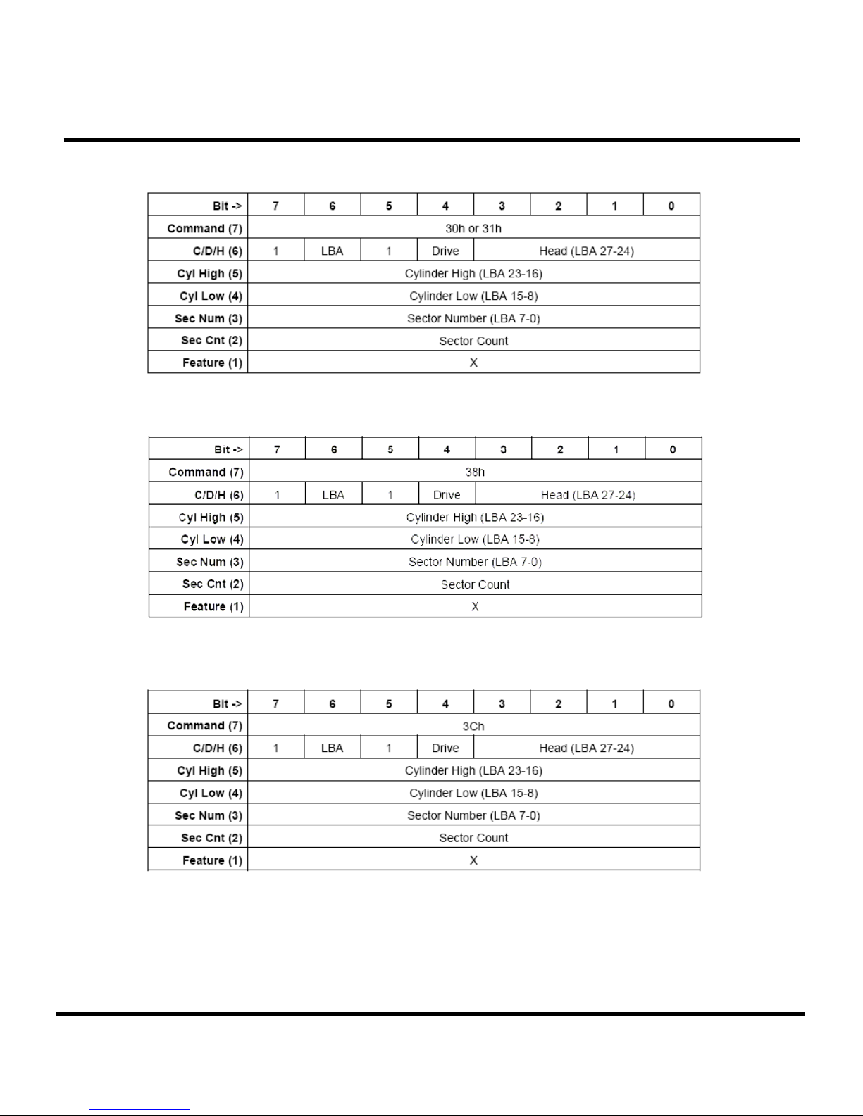
T
S
2
G
~
8
G
C
F
2
6
6
T
S
2
G
~
8
G
C
T
S
2
G
~
8
Write Sector(s) - 30h or 31h
G
C
F
F
2
2
6
6
6
6
Write Sector(s) without Erase - 38h
266X CompactFlash Card
Write Verify - 3Ch
Transcend Information Inc.
77
Page 78

T
S
2
G
~
8
G
C
F
T
S
2
G
~
8
G
~
8
G
G
T
S
2
Error Posting
C
C
F
F
2
2
2
6
6
6
6
6
6
266X CompactFlash Card
Transcend Information Inc.
78
Page 79
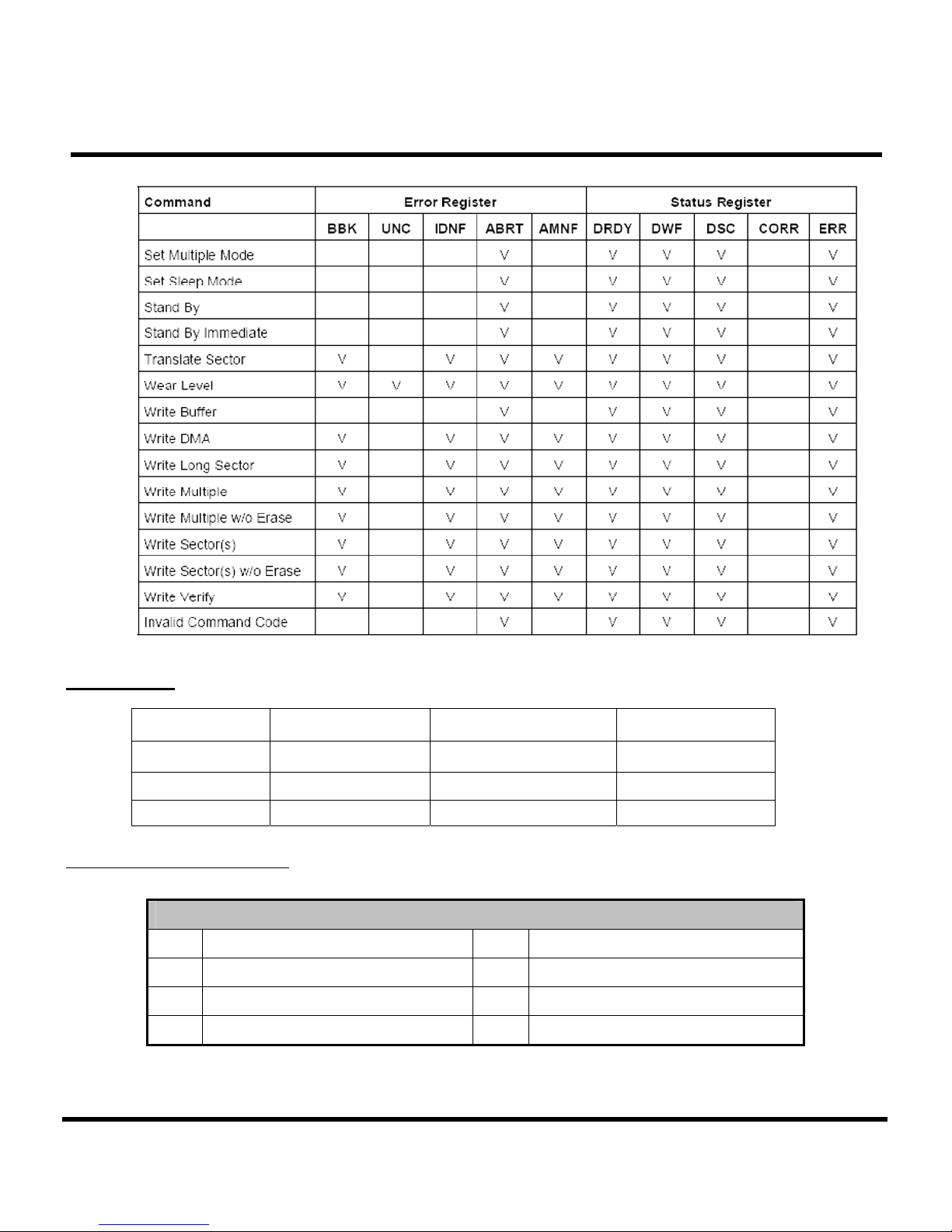
T
T
T
S
S
S
2
2
2
G
G
G
~
8
G
C
F
2
6
6
~
~
8
8
G
G
C
C
F
F
2
2
6
6
6
6
266X CompactFlash Card
Error and Status Register summarizes the valid status and error value for all the CF-ATA Command set.
C.H.S. Table
Capacity C H S
2GB 3949 16 63
4GB 7899 16 63
8GB 15798 16 63
SMART Command Set
SMART Command Set
D0h Read Data D4h Execute OFF-LINE Immediate
D1h Read Attribute Threshold D8h Enable SMART Operations
D2h Enable/Disable Autosave D9h Disable SMART Operations
SMART Feature Register Values
D3h Save Attribute Values DAh Return Status
1. If reserved size is below the Threshold, the status can be read from Cylinder register by Return Status command
(DAh).
Transcend Information Inc.
79
Page 80

T
S
2
G
~
8
G
C
F
2
6
6
T
S
2
G
~
8
G
C
T
S
2
G
~
8
SMART Data Structure
F
G
C
F
BYTE F / V Decription
0-1 X Revision code
2-361 X Vendor specific
362 V Off line data collection status
363 X Self-test execution status byte
364-365 V Total time in seconds to complete off-line data collection activity
366 X Vendor specific
367 F Off-line data collection capability
368-369 F SMART capability
370 F
371 X Vendor specific
372 F Short self-test routine recommended polling time (in minutes)
2
2
6
6
6
6
266X CompactFlash Card
Error logging capability
7-1 Reserved
0 1=Device error logging supported
373 F Extended self-test routine recommended polling time (in minutes)
374 F Conveyance self-test routine recommended polling time (in minutes)
375-385 R Reserved
386-395 F Date Code
396 V Number of MU in device (0~n)
397+(n*6) V MU number
398+(n*6) V MU data block
400+(n*6) V MU spare block
401+(n*6) V Init. Bad block
402+(n*6) V Last Defect Bad block ( Newest state)
511 V Data structure checksum
F=the content of the byte is fixed and does not change.
V=the content of the byte is variable and may change depending on the state of the device or
the commands executed by the device.
X=the content of the byte is vendor specific and may be fixed or variable.
R=the content of the byte is reserved and shall be zero.
* 4 Byte value : [MSB] [2] [1] [LSB]
Above technical information is based on CFA standard data and tested to be reliable. However, Transcend makes no
warranty, either expressed or implied, as to its accuracy and assumes no liability in connection with the use of this
product. Transcend reserves the right to make changes in specifications at any time without prior notice.
Transcend Information Inc.
80
 Loading...