

现货库存、技术资料、百科信息、热点资讯,精彩尽在鼎好!
TOSHIBA Photocoupler GaAℓAs IRed & Photo−IC
TLP651
Digital Logic Ground Isolation
Line Receiver
Microprocessor System Interfaces
Switching Power Supply Feedback Control
Analog Signal Isolation
The TOSHIBA TLP651 consists of a GaAℓAs high
diode and a high speed detector of one chip photo diode−transistor.
This unit is 8
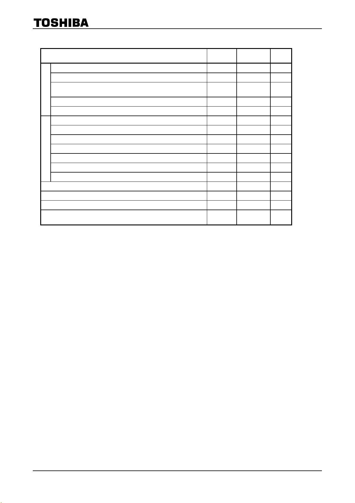
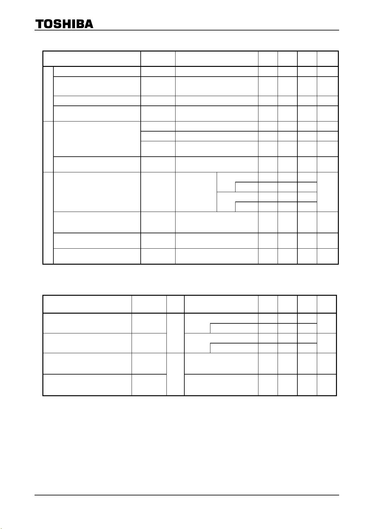
TLP651 has internal base connection. This base pin should be used for
analog application or enable operation. If base pin is open, output signal
will be noisy by environmental condition. For this case, TLP650 is
suitable.
• Isolation voltage: 5000V
• Switching speed: t
• TTL compatible
• UL recognized: UL1577, file no. E67349
• BSI approved: BS EN60065: 2002
−lead DIP.
rms
= 0.3μs (typ.)
pHL
t
= 0.5μs (typ.) (RL = 1.9kΩ)
pLH
Certificate no. 7613
BS EN60950-1: 2002
Certificate no. 7614
(min.)
−output light emitting
Pin Configuration
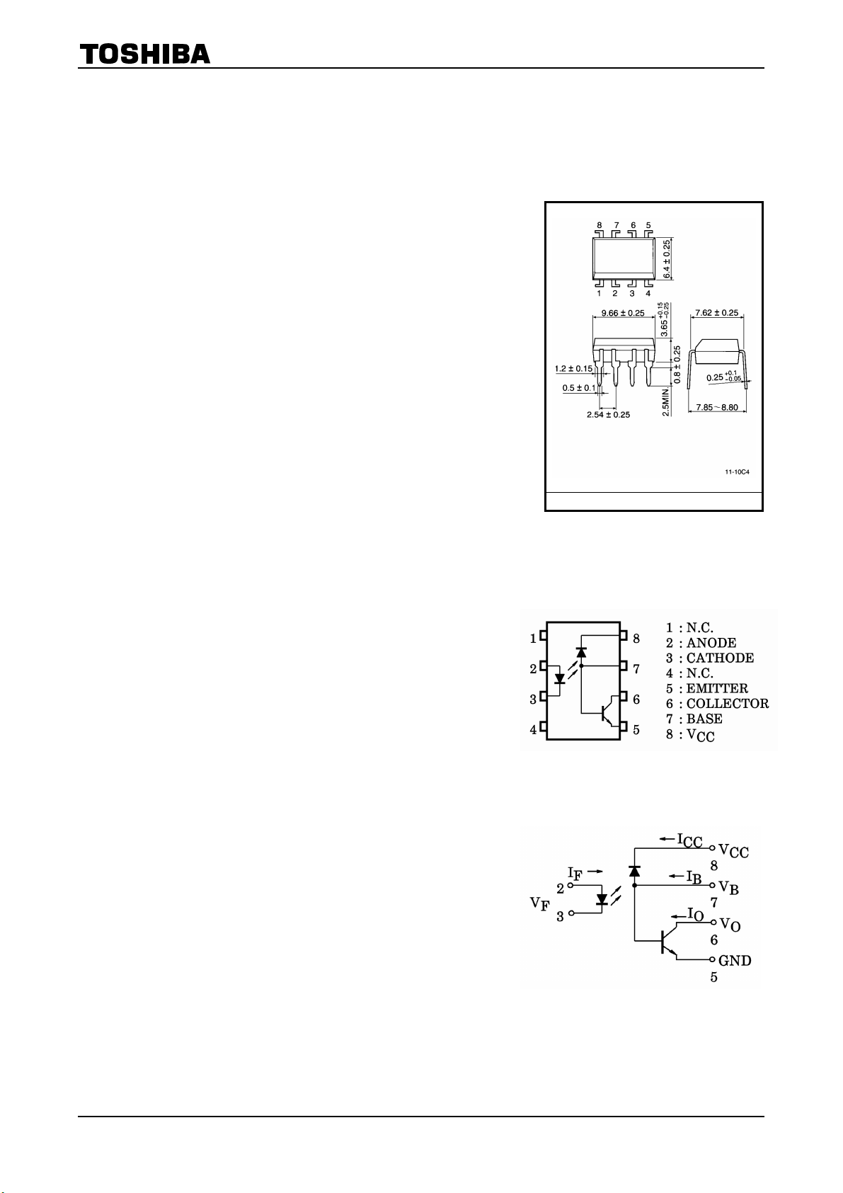
TOSHIBA 11−10C4
Weight: 0.54g
(top view)
TLP651
Unit in mm
Schematic
2007-10-01 1
TLP651
Absolute Maximum Ratings
Characteristic Symbol Rating Unit
Forward current (Note 1) IF 25 mA
Pulse forward current (Note 2) IFP 50 mA
Peak transient forward
current (Note 3)
LED
Reverse voltage VR 5 V
Diode power dissipation (Note 4) PD 45 mW
Output current IO 8 mA
Peak output current IOP 16 mA
Output voltage VO −0.5~15 V
Supply voltage VCC −0.5~15 V
Detector
Base current IB 5 mA
Emitter−base reverse voltage VEB 5 V
Output power dissipation (Note 5) PO 100 mW
Operating temperature range T
Storage temperature range T
Lead solder temperature (10s) (Note 6) T
Isolation voltage
(AC, 1min., R.H.≤ 60%) (Note 7)
(Ta = 25°C)
1 A
I
FPT
−55~100 °C
opr
−55~125 °C
stg
260 °C
sol
5000 V
BV
S
rms
Note: Using continuously under heavy loads (e.g. the application of high temperature/current/voltage and the
significant change in temperature, etc.) may cause this product to decrease in the reliability significantly even
if the operating conditions (i.e. operating temperature/current/voltage, etc.) are within the absolute maximum
ratings.
Please design the appropriate reliability upon reviewing the Toshiba Semiconductor Reliability Handbook
(“Handling Precautions”/“Derating Concept and Methods”) and individual reliability data (i.e. reliability test
report and estimated failure rate, etc).
(Note 1) Derate 0.8mA above 70°C.
(Note 2) 50% duty cycle,1ms pulse width.
Derate 1.6mA / °C above 70°C.
(Note 3) Pulse width ≤ 1μs, 300pps.
(Note 4) Derate 0.9mW / °C above 70°C.
(Note 5) Derate 2mW / °C above 70°C.
(Note 6) Soldering portion of lead: Up to 2mm from the body of the device.
(Note 7) Device considered a two terminal device: Pins 1, 2, 3 and 4 shorted together and pins 5, 6, 7 and 8 shorted
together.
2
2007-10-01
TLP651
Electrical Characteristics
Characteristic Symbol Test Condition Min. Typ. Max. Unit
Forward voltage VF IF = 16mA ― 1.65 1.85 V
Forward voltage
temperature coefficient
LED
Reverse current IR VR = 5V ― ― 10 μA
Capacitance between
terminal
High level output
current
Detector
High level supply
voltage
Current transfer ratio IO / IF
Low level output
voltage
Coupled
Isolation resistance RS
Capacitance between
input to output
Switching Characteristics
(Ta = 25°C)
/ ΔTa IF = 16mA ― −2 ― mV / °C
ΔV
F
VF = 0, f = 1MHz ― 45 ― pF
C
T
I
IF = 0mA, VCC = VO = 5.5V ― 3 500 nA
OH (1)
I
IF = 0mA, VCC = VO = 15V ― ― 5 μA
OH (2)
I
= 0mA, V
F
I
I
CCH
V
C
OH
OL
Ta = 70°C
IF = 0mA, VCC = 15V ― 0.01 1 μA
I
= 16mA
F
= 4.5V
V
CC
= 0.4V
V
O
I
= 16mA, VCC = 4.5V,
F
VS = 0, f = 1MHz (Note 7) ― 0.8 ― pF
S
= 1.1mA
I
O
(Rank 0: I
R.H.≤ 60%, V
(Note 7)
(Ta = 25°C, VCC = 5V)
= VO = 15V
CC
= 2.4mA)
O
= 500VDC
S
― ― 250 μA
Ta = 25°C 10 30 ―
Rank: O 19 30 ―
Ta = 0~70°C 5 ― ―
Rank: O 15 ― ―
― ― 0.4 V
10
1014 ― Ω
5×10
%
Test
Characteristic Symbol
Propagation delay time
(H→L)
Propagation delay time
(L→H)
Common mode transient
immunity at logic high
output (Note 8)
Common mode transient
immunity at logic low
output (Note 8)
t
t
C
C
pHL
pLH
MH
ML
Cir−
cuit
1
2
Test Condition Min. Typ. Max. Unit
IF = 0→16mA, VCC = 5V, ― 0.2 0.8
=4.1kΩ Rank O: RL=1.9kΩ ― 0.3 0.8
R
L
IF = 16→ 0mA, VCC = 5V, ― 1.0 2.0
R
=4.1kΩ Rank O: RL=1.9kΩ ― 0.5 1.2
L
I
= 0mA, VCM = 200V
F
RL = 4.1kΩ
(Rank O: R
I
=16mA, VCM = 200V
F
RL = 4.1kΩ
(Rank O: R
= 1.9kΩ)
L
= 1.9kΩ)
L
p−p
p−p
― 400 ― V / μs
― −1000 ― V / μs
μs
μs
3
2007-10-01
 Loading...