

查询TC55V8512FT-12供应商
TC55V8512J/FT-12,-15
TOSHIBA MOS DIGITAL INTEGRATED CIRCUIT SILICON GATE CMOS
524,288-WORD BY 8-BIT CMOS STATIC RAM
DESCRIPTION
The TC55V8512J/FT is a 4,194,304-bit high-speed static random access memory (SRAM) organized as 524,288
words by 8 bits. Fabricated using CMOS technology and advanced circuit techniques to provide high speed, it
operates from a single 3.3 V power supply. Chip enable (CE ) can be used to place the device in a low-power mode,
and output enable (OE ) provides fast memory access. This device is well suited to cache memory applications
where high-speed access and high-speed storage are required. All inputs and outputs are directly LVTTL
compatible. The TC55V8512J/FT is available in plastic 36-pin SOJ and 44-pin TSOP with 400mil width for high
density surface assembly.
FEATURES
• Fast access time (the following are maximum values)
TC55V8512J/FT-12:12 ns
TC55V8512J/FT-15:15 ns
• Low-power dissipation
(the following are maximum values)
Cycle Time 12 15 20 25 ns
Operation (max) 170 140 130 110 mA
Standby:4 mA (both devices)
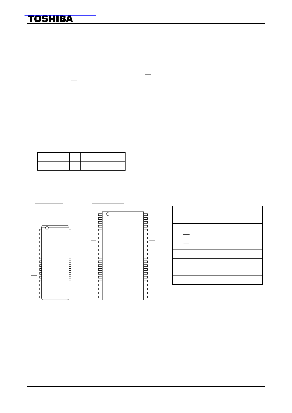
PIN ASSIGNMENT
36 PIN SOJ
A17
1 36
A3
2 35
A2
3 34
A1
4 33
A0
5 32
6 31
CE OE
I/O1
7 30
I/O2
8 29
DD
V
9 28
GND
10 27
I/O3
11 2 6
I/O4
12 25
13 24
WE
A16
14 23
A15
15 22
A14
16 21
A13
17 20
A18
18 19
44 PIN TSOP
(TOP VIEW)
NC
NC
A17
A3
NC
A4
A5
A6
A7
I/O8
I/O7
GND
DD
V
I/O6
I/O5
A8
A9
A10
A11
A12
NU
A2
A1
A0
I/O1
I/O2
DD
V
GND
I/O3
I/O4
WE
A16
A15
A14
A13
A18
NC
NC
1 44
2 43
3 42
4 41
5 40
6 39
7 38
8 37
9 36
10 35
11 3 4
12 33
13 32
14 31
15 30
16 29
17 28
18 27
19 26
20 25
21 24
22 23
• Single power supply voltage of 3.3 V ± 0.3 V
• Fully static operation
• All inputs and outputs are LVTTL compatible
• Output buffer control using
OE
• Package:
SOJ36-P-400-1.27 (J) (Weight: 1.35 g typ)
TSOP II44-P-400-0.80 (FT) (Weight: 0.45 g typ)
NC
NC
NC
A4
A5
A6
A7
OECE
I/O8
I/O7
GND
DD
V
I/O6
I/O5
A8
A9
A10
A11
A12
NU
NC
NC
PIN NAMES
A0 to A18 Address Inputs
I/O1 to I/O8 Data Inputs/Outputs
CE
WE Write Enable Input
OE
VDD Power (+3.3 V)
GND Ground
NC No Connection
NU Not Usable (Input)
Chip Enable Input
Output Enable Input
(TC55V8512J)
(TC55V8512FT)
2001-12-19 1/10
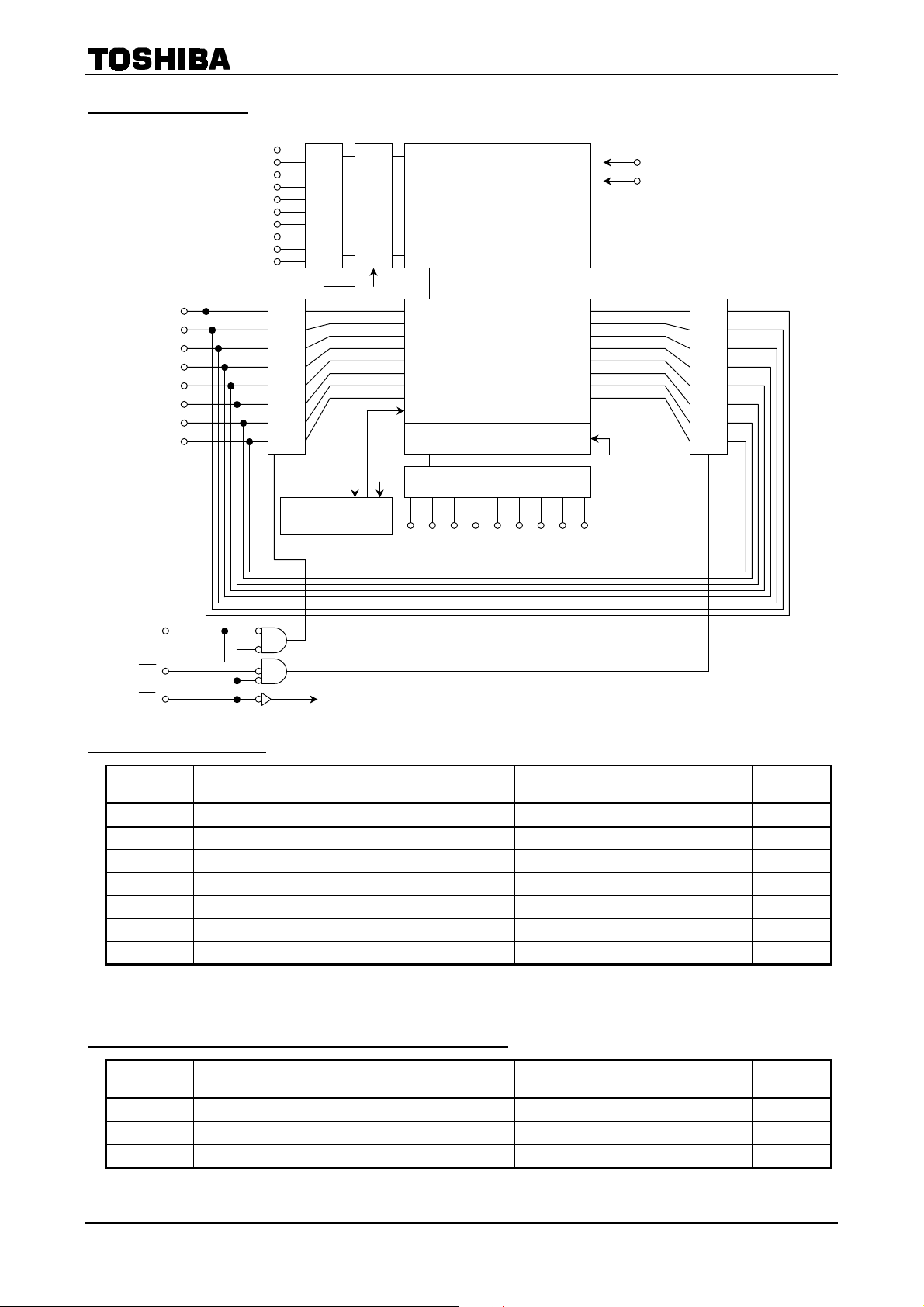
BLOCK DIAGRAM
TC55V8512J/FT-12,-15
I/O1
I/O2
I/O3
I/O4
I/O5
I/O5
I/O7
I/O8
A0
A1
A4
A8
A9
A12
A14
A15
A16
A17
BUFFER
ROW ADDRESS
BUFFER
DATA INPUT
CLOCK
GENERATOR
MEMORY CELL ARRAY
ROW
DECODER
CE
COLUMN DECODER
COLUMN ADDRESS BUFFER
A2 A3 A5 A6 A7 A10 A11A13
512 × 1,024 × 8
(4,194,304)
SENSE AMP
VDD
GND
BUFFER
DATA OUTPUT
CE
A18
WE
OE
CE
CE
MAXIMUM RATINGS
SYMBOL RATING VALUE UNIT
V
DD
V
IN
V
I/O
P
D
T
solder
T
stg
T
opr
*: −1.5 V with a pulse width of 20%・t
**: V
DD
DC RECOMMENDED OPERATING CONDITIONS
SYMBOL PARAMETER MIN TYP MAX UNIT
Power Supply Voltage −0.5 to 4.6 V
Input Terminal Voltage −0.5* to 4.6 V
Input/Output Terminal Voltage −0.5* to VDD + 0.5** V
Power Dissipation 1.4 W
Soldering Temperature (10s) 260 °C
Storage Temperature −65 to 150 °C
Operating Temperature −10 to 85 °C
min (4 ns max)
+ 1.5 V with a pulse width of 20%・t
RC
min (4 ns max)
RC
(Ta ==== 0° to 70°C)
VDD Power Supply Voltage 3.0 3.3 3.6 V
VIH Input High Voltage 2.0 VDD + 0.3** V
VIL Input Low Voltage −0.3* 0.8 V
*: −1.0 V with a pulse width of 20%・t
**: V
+ 1.0 V with a pulse width of 20%・t
DD
min (4 ns max)
RC
min (4 ns max)
RC
2001-12-19 2/10
TC55V8512J/FT-12,-15
DC CHARACTERISTICS
SYMBOL PARAMETER
IIL
ILO
I
I (NU)
VOH Output High Voltage
VOL Output Low Voltage
I
Operating Current
DDO
I
DDS1
I
DDS2
Input Leakage Current
(Except NU pin)
Output Leakage
Current
Input Current
(NU pin)
Standby Current
(Ta ==== 0° to 70°C, VDD ==== 3.3 V ±±±± 0.3 V)
TEST CONDITION MIN TYP MAX UNIT
VIN = 0 to VDD −1 1 µA
= VIH or WE = VIL or OE = VIH,
CE
V
= 0 to VDD
OUT
VIN = 0 to 0.8 V −1 20
V
= 0 to 0.2 V −1 1
IN
IOH = −2 mA 2.4
= −100 µA VDD − 0.2
I
OH
IOL = 2 mA 0.4
= 100 µA 0.2
I
OL
= VIL, I
CE
= VIH,
OE
Other Input = V
= VIH, Other Input = VIH or VIL 50
CE
= VDD − 0.2 V, Other Input = VDD − 0.2 V or 0.2 V 4
CE
OUT
= 0 mA,
IH/VIL
−1 1 µA
t
= 12 ns 170
cycle
t
= 15 ns 140
cycle
t
= 20 ns 130
cycle
= 25 ns 110
t
cycle
µA
V
mA
mA
CAPACITANCE
SYMBOL PARAMETER TEST CONDITION MAX UNIT
CIN Input Capacitance VIN = GND 6 pF
C
Input/Output Capacitance V
I/O
Note: This parameter is periodically sampled and is not 100% tested.
(Ta ==== 25°C, f ==== 1 .0 MHz)
= GND 8 pF
I/O
OPERATING MODE
MODE
Read L L H Output I
Write L * L Input I
Outputs Disable L H H High Impedance I
Standby H * * High Impedance I
* : Don’t care
Note: The NU pin must be left unconnected or tied to GND or a voltage level of less than 0.8 V.
You must not apply a voltage of more than 0.8 V to the NU.
CE
WE I/O1 to I/O8 POWER
OE
DDO
DDO
DDO
DDS
2001-12-19 3/10

TC55V8512J/FT-12,-15
AC CHARACTERISTICS
(Ta ==== 0° to 70°C
(See Note 1)
, VDD ==== 3.3 V ±±±± 0.3 V)
READ CYCLE
TC55V8512J/FT
SYMBOL PARAMETER
tRC Read Cycle Time 12 15
t
Address Access Time 12 15
ACC
tCO Chip Enable Access Time 12 15
tOE Output Enable Access Time 6 8
tOH Output Data Hold Time from Address Change 3 4
t
Output Enable Time from Chip Enable 3 4
COE
t
Output Enable Time from Output Enable 1 1
OEE
t
Output Disable Time from Chip Enable 7 8
COD
t
Output Disable Time from Output Enable 7 8
ODO
-12 -15
MIN MAX MIN MAX
WRITE CYCLE
TC55V8512J/FT
SYMBOL PARAMETER
-12 -15
MIN MAX MIN MAX
UNIT
ns
UNIT
tWC Write Cycle Time 12 15
tWP Write Pulse Width 8 9
tCW Chip Enable to End of Write 10 12
tAW Address Valid to End of Write 10 12
tAS Address Setup Time 0 0
tWR Write Recovery Time 0 0
tDS Data Setup Time 7 8
tDH Data Hold Time 0 0
t
Output Enable Time from Write Enable 1 1
OEW
t
Output Disable Time from Write Enable 7 8
ODW
AC TEST CONDITIONS Fig.1
PARAMETER TEST CONDITION
Input Pulse Level 3.0 V/ 0.0 V
Input Pulse Rise and Fall Time 2 ns
Input Timing Measurement
Reference Level
Output Timing Measurement
Reference Level
1.5 V
1.5 V
I/O pin
Z0 = 50 Ω
CL = 30 pF
= 1.5 V
V
L
RL = 50 Ω
CL = 5 pF
(For t
t
ODO
I/O pin
, t
COE
OEW
, t
3.3 V
OEE
and t
1200 Ω
870 Ω
, t
COD
ODW
ns
,
)
Output Load Fig.1
2001-12-19 4/10

TIMING DIAGRAMS
READ CYCLE
Address
(See Note 2)
TC55V8512J/FT-12,-15
t
RC
CE
OE
D
OUT
Hi-Z
WRITE CYCLE 1 ( CONTROLLED)
WE
Address
t
AS
t
ACC
t
CO
t
(See Note 6)
t
(See Note 6)
t
INDETERMINATE
(See Note 5)
OE
t
AW
t
WC
t
OH
(See Note 6)
t
(See Note 6)
t
VAL I D DATA O UT
INDETERMINATE
Hi-Z
t
WP
t
WR
WE
t
CW
CE
D
OUT
D
(See Note 6)
t
(See Note 3) Hi-Z
INDETERMINATE
IN
t
DS
VAL I D DATA IN
t
t
DH
(See Note 6)
(See Note 4)
INDETERMINATE
2001-12-19 5/10

TC55V8512J/FT-12,-15
WRITE CYCLE 2 ( CONTROLLED)
Address
WE
CE
D
OUT
D
IN
CE
t
AS
Hi-Z
t
COE
(See Note 5)
(See Note 6)
t
WC
t
AW
t
CW
(See Note 6)
t
ODW
INDETERMINATE
t
WP
t
DS
VAL I D DATA IN
t
t
DH
WR
Hi-Z
2001-12-19 6/10

TC55V8512J/FT-12,-15
Note:
(1) Operating temperature (Ta) is guaranteed for transverse air flow exceeding 400 linear feet per minute.
(2)
WE remains HIGH for the Read Cycle.
(3) If CE goes LOW coincident with or after WE goes LOW, the outputs will remain at high impedance.
(4) If CE goes HIGH coincident with or before WE goes HIGH, the outputs will remain at high
impedance.
(5) If
OE is HIGH during the write cycle, the outputs will remain at high impedance.
(6) The parameters specified below are measured using the load shown in Fig.1.
(A) t
(B) t
COE
COD
, t
, t
OEE
ODO
・・・・・・・・・・・・・・・・・
, t
OEW
, t
・・・・・・・・・・・・・・・・
ODW
Output Enable Time
Output Disable Time
CE,
OE
WE
(A)
D
OUT
Hi-Z
0.2 V
0.2 V
INDETERMINATE
VAL I D DATA O UT
(B)
INDETERMINATE
0.2 V
0.2 V
Hi-Z
2001-12-19 7/10

PACKAGE DIMENSIONS
TC55V8512J/FT-12,-15
Weight: 1.35 g (typ)
2001-12-19 8/10

PACKAGE DIMENSIONS
TC55V8512J/FT-12,-15
Weight: 0.45 g (typ)
2001-12-19 9/10

TC55V8512J/FT-12,-15
RESTRICTIONS ON PRODUCT USE
• TOSHIBA is continually working to improve the quality and reliability of its products. Nevertheless, semiconductor
devices in general can malfunction or fail due to their inherent electrical sensitivity and vulnerability to physical
stress. It is the responsibility of the buyer, when utilizing TOSHIBA products, to comply with the standards of
safety in making a safe design for the entire system, and to avoid situations in which a malfunction or failure of
such TOSHIBA products could cause loss of human life, bodily injury or damage to property.
In developing your designs, please ensure that TOSHIBA products are used within specified operating ranges as
set forth in the most recent TOSHIBA products specifications. Also, please keep in mind the precautions and
conditions set forth in the “Handling Guide for Semiconductor Devices,” or “TOSHIBA Semiconductor Reliability
Handbook” etc..
• The TOSHIBA products listed in this document are intended for usage in general electronics applications
(computer, personal equipment, office equipment, measuring equipment, industrial robotics, domestic appliances,
etc.). These TOSHIBA products are neither intended nor warranted for usage in equipment that requires
extraordinarily high quality and/or reliability or a malfunction or failure of which may cause loss of human life or
bodily injury (“Unintended Usage”). Unintended Usage include atomic energy control instruments, airplane or
spaceship instruments, transportation instruments, traffic signal instruments, combustion control instruments,
medical instruments, all types of safety devices, etc.. Unintended Usage of TOSHIBA products listed in this
document shall be made at the customer’s own risk.
• The products described in this document are subject to the foreign exchange and foreign trade laws.
• The information contained herein is presented only as a guide for the applications of our products. No
responsibility is assumed by TOSHIBA CORPORATION for any infringements of intellectual property or other
rights of the third parties which may result from its use. No license is granted by implication or otherwise under
any intellectual property or other rights of TOSHIBA CORPORATION or others.
000707EBA
• The information contained herein is subject to change without notice.
2001-12-19 10/10
 Loading...