Toshiba SD-4700, SD-5700 Service manual

FILE NO. 813-200104
SUPPLEMENT
SERVICE MANUAL
DIGITAL VIDEO
DVD VIDEO/AUDIO PLAYER
SD-4700
®
SD-5700
– SUMMARY
This service manual covers only the different points from the service manual, file no. 810-200108,
for model SD-3750 since SD-4700, SD-5700 is basically the same designing as SD-3750.
Please refer to the file no. 810-200108 for other information.
––
–
––
Jan., 2002
S

LASER BEAM CAUTION LABEL
When the power supply is being turned on, you may not remove this laser cautions label. If it removes, radiation of a laser
may be recceived.
PREPARATION OF SERVICING
Pickup Head consists of a laser diode that is very susceptible to external static electricity.
Although it operates properly after replacement, if it was subject to electrostatic discharge during replacement,
its life might be shortened. When replacing, use a conductive mat, soldering iron with ground wire, etc. to
protect the laser diode from damage by static electricity.
And also, the LSI and IC are same as above.
Note:
Ground conductive
wrist strap for body.
Soldering iron
with ground wire
or ceramic type
Conductive mat
®
: Only for SD-5700.
SD-4700 is not provided with HDCD decoder.
1M
W
The ground resistance
between the ground line
and the ground is less than 10W.

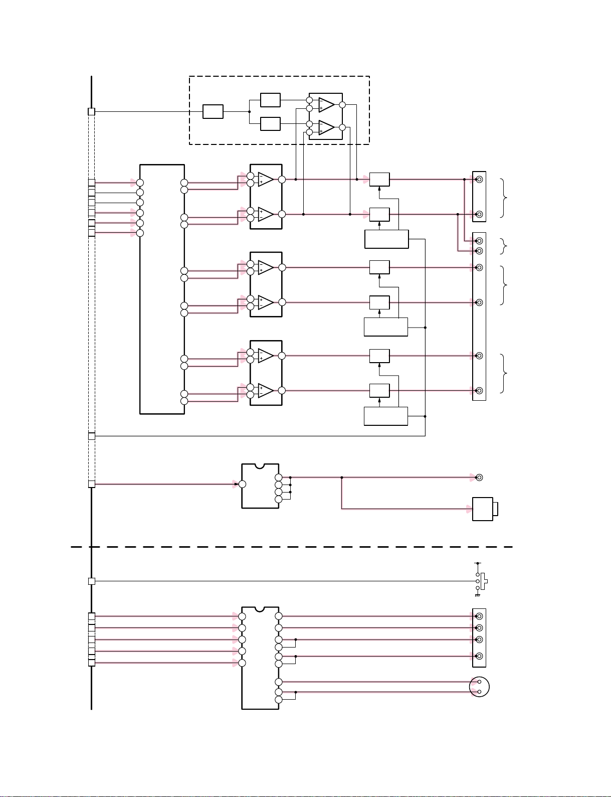
4. BLOCK DIAGRAM
Output Block Diagram
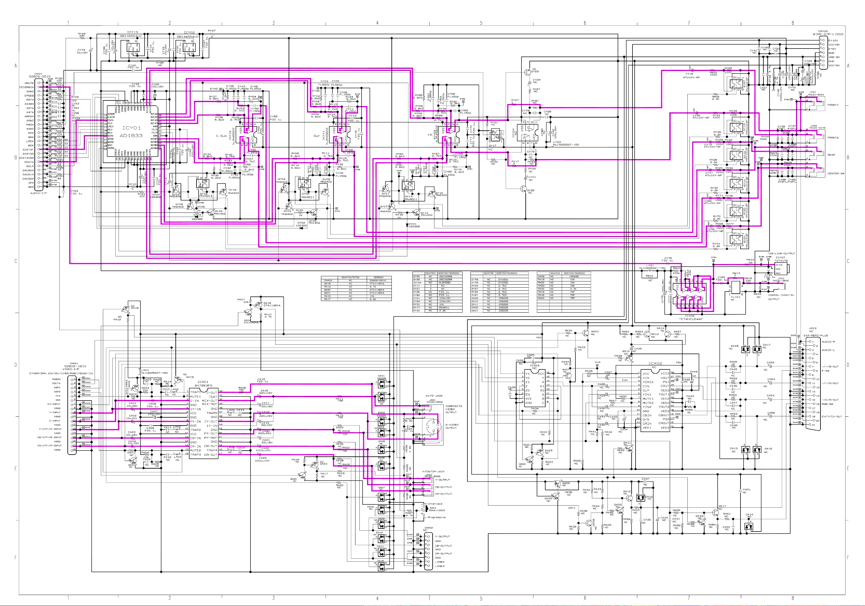
5. CIRCUIT DIAGRAM
Output Circuit Diagram
SAFETY PRECAUTION
NOTICE
ABBREVIATIONS
1. Integrated Circuit (IC)
2. Capacitor (Cap)
3. Resistor (Res)
CONTENTS
SECTION 3
SERVICING DIAGRAMS
SECTION 4
PARTS LIST
4. EXPLODED VIEWS
4-1. Packing Assembly
4-2. Chassis Assembly
4-3. Mechanism Assembly
5. PARTS LIST

Output Block Diagram
CNY01
G+6DB
ADATAF
BCK
LRCK
SDATA
ADATAS
ADATACSW
HMUTE
ICE958
IN
SD-5700
QY29
QY17
4
SW
SW
QY25
SW
ICY01
AD1833
AUDIO DAC
Lch SIGNAL
1
OUT LP1
17
16
15
20
18
19
1
2
20
OUT LN1
18
17
15
21
22
OUT RN1
OUT RP1
OUT LP1
OUT LN1
OUT RN2
OUT RP2
OUT LP3
OUT LN3
OUT RN3
OUT RP3
35
36
47
48
37
38
45
46
39
40
HMUTE
DIGITAL AUDIO SIGNAL
2
Rch SIGNAL
Lch SIGNAL
Rch SIGNAL
Lch SIGNAL
Rch SIGNAL
ICY03
NJM4580E
AMP
2
3
5
6
ICY11
NJM4580E
AMP
2
3
5
6
ICY12
NJM4580E
AMP
2
3
5
6
ICY09
TC74HCU04AF
BUFFER
13
2
4
6
8
ICY04
NJM4580
3
4
6
5
1
7
1
7
1
7
1
7
QY01
QY07
QY13
QY14
QY16
QY02
QY04
QY05
QY08
QY09
QY03
QY06
QY12
QY15
QY18
QY27
MUTE
QY19
MUTE
MUTE
CONTROL
QY10
MUTE
QY11
MUTE
MUTE
CONTROL
QY20
MUTE
QY21
MUTE
MUTE
CONTROL
JY01
JY02
Lch
Rch
Lch
Rch
Lch
Rch
Lch
Rch
FRONT1
FRONT2
REAR
SENTER SW
JY03
DIGITAL OUTPUT
(COAXIAL)
ICY07
TOTX179
CNY01
CNX01
Y (I/P)/ G
C
B
(I/P)/ B
R
(I/P)/ R
C
IPX
AUDIO
VIDEO
25
9
Y
11
C
13
15
17
ICX01
BH7863FS
VIDEO LPF/AMP
5
3
8
12
14
17
19
22
21
30
29
32
25
24
5V
JX02
H : Interlace
L : Progressive
R
P
P
B
Y
COMPOSITE
VIDEO
JX01
C
S VIDEO
Y
Fig. 3-1-1

Output Circuit Diagram
Fig. 3-2-1

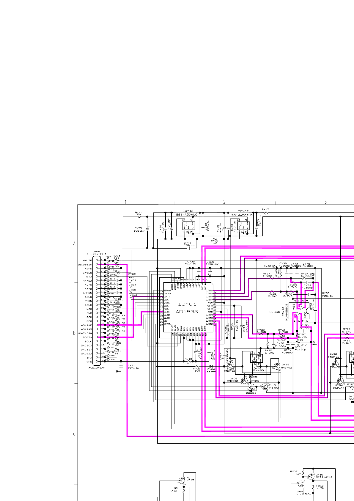
Output Circuit Diagram
 Loading...