

Page 1
SERVICE MANUAL
DOCUMENT CREATED IN JAPAN, DECEMBER, 2005
DVD VIDEO PLAYER
FILE NO. 810-200592GRI
INTERNAL PUBLICATION
SD-3990SU
SD-3990SC
The above model is classified as a green products (*1), as indicated by the underlined serial numbers.
This
Service Manual describes replacement parts for green products. When repairing any green
products,
For
TOSHIBA CORPORATION 2005
use the parts described in this manual and lead-free solder (*2).
(*1) and (*2), see the next page.
Dec. 2005 (TO) GREEN
Page 2

(*1) GREEN PRODUCT PROCUREMENT
The EC is actively promoting the WEEE & RoHS Directives that define standards for recycling
and reuse of Waste Electrical and Electronic Equipment and for the Restriction of the use of
certain Hazardous Substances. From July 1, 2006, the RoHS Directive will prohibit any
marketing of new products containing lead.
Increasing attention is given to issues related to the global environmental. Toshiba Corporation
recognizes environmental protection as a key management tasks, and is doing its utmost to
enhance and improve the quality and scope of its environmental activities. In line with this,
Toshiba proactively promotes Green Procurement, and seeks to purchase and use products,
parts and materials that have low environmental impacts.
Green procurement of parts is not only confined to manufacture. The same green parts used in
manufacture must also be used as replacement parts.
(*2) LEAD-FREE SOLDER
This product is manufactured using lead-free solder as a part of a movement within the CE
industry at large to be environmentally responsible. Lead-free solder must be used in the servicing
and repair of this product.
The melting temperature of lead-free solder is higher than that of leaded solder by 86°F to 104°F
(30°C to 40°C). Use of a soldering iron designed for lead-based solders to repair product made
with lead-free solder may result in damage to the component and or PCB being soldered. Great
care should be made to ensure high-quality soldering when servicing this product especially
when soldering large components, through-hole pins, and on PCBs as the level of heat
required to melt lead-free solder is high.
WARNING
This product is manufactured using lead free solder.
DO NOT USE LEAD BASED SOLDER TO REPAIR THIS PRODUCT !
Page 3

CONTENTS
ˊ
ˊ
ˊ
ˊ
ˊ
ˊ
ˊ
1ˊPRINTEDWIRINGBOARD AND SCHEMATIC DIAGRAM
Printed Wiring Board and Schematic Diagram
BLOCK DIAGRAMS
2
SET Block Diagram
Power Supply Block Diagram
CIRCUITDIAGRAMS
3
Power Supply Circuit Diagram
(Terminal Voltage Lists)
Front Display Circuit Diagram
Main chip & SDRAM Circuit Diagram
Power & AV Output Circuit Diagram
FE & Driver Circuit Diagram
Flash & SRAM I/F Circuit Diagram
Audio Circuit Diagram
PC BOARDS
4
Power Supply PC Board(Top side)
Main PC Board(Top side)
Main PC Board(Bottom side)
Front Display PC Board(Top side)
Front PC Board(Bottom side)
IC BLOCK DIAGRAMS
5
PARTS LIST
6
EXPLODED VIEWS
7
SPECIFICATIONS
8
Page 4
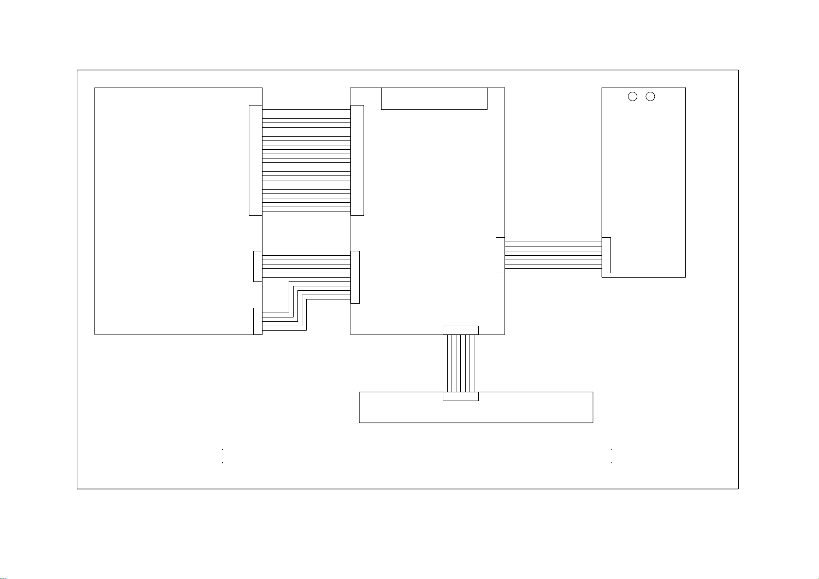
DVD MECHA
CON2
CON1
J3
24
23
22
21
20
19
18
17
16
15
14
13
12
11
10
9
8
7
6
5
4
3
2
1
GND-LD
DVD-LD
NC
HFM
MD
CD-LD
VR-DVD
VR-CD
NC
E
VCC
VC(VREF)
GND/PD
F
B
A
RF
CD/DVD SW
D
C
TT+
F+
F-
24
23
22
21
20
19
18
17
16
15
14
13
12
11
10
9
8
7
6
5
4
3
2
1
CN201
1
2
3
4
5
6
5
4
3
2
1
SLED+9
SLEDHOME SW
GND
SP+
SPLOAD+
LOADOUT SW
GND
IN SW
1A
2A
3A
4A
5A
6A
7A
8A
9A
10A
11A
CN203A
AUDIO/VIDEO OUTPUT
JR502B
MPEG BORAD
J1
1234567
STB
IR
VCC
DAT IN
CLK
GND
DATA OUT
CN504
AC IN
POWER UNIT
7
6
5
4
3
2
1
+5V
GND
+12V
-12V
5VSTB
GND
POWER ON
7
6
5
4
3
2
1
CN902
1234567
J1
FRONT PCB
Printed Wiring Board and Schematic Diagram
Page 5
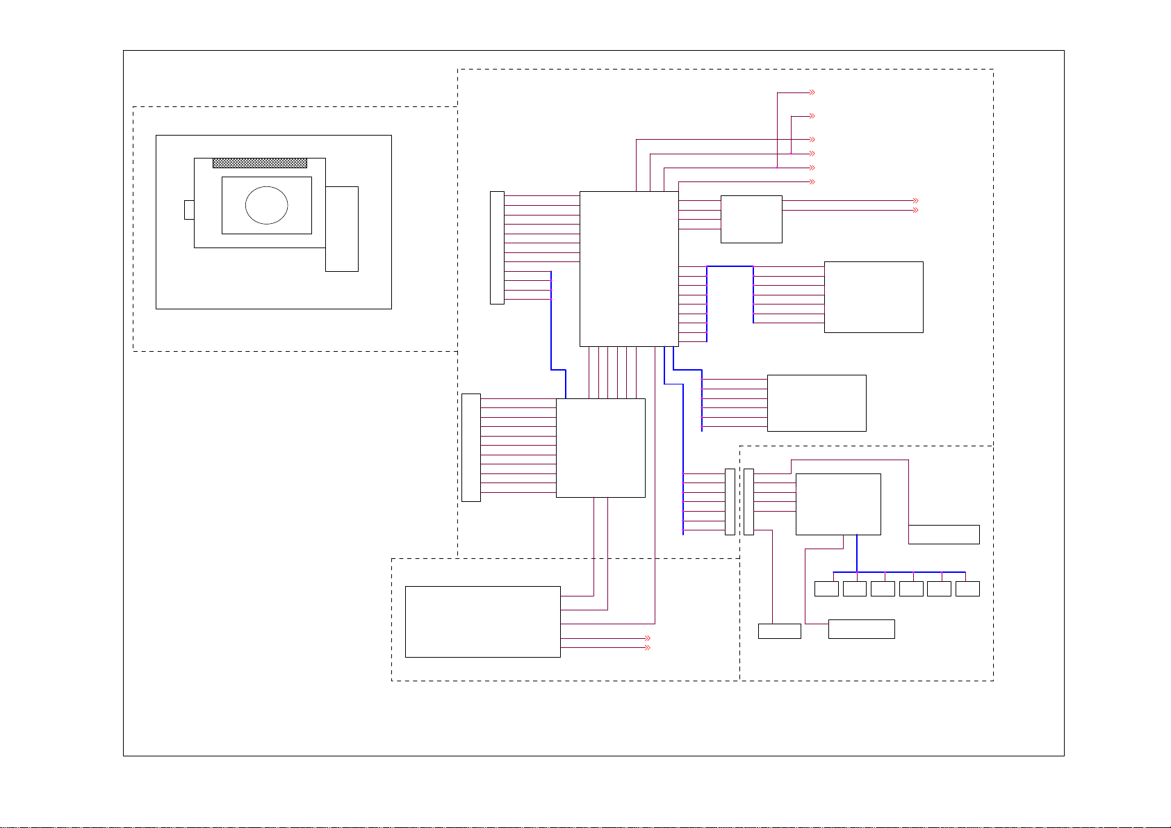
PICK UP
SAMSUNG
S75
CN201
MPEG BORAD
A
B
C
D
E
F
DVD LD
CD LD
TACTTACTFACTFACT+
U101
ZORAN
ZR36882ELCG
ENCODER
DOBY AC-3 ,DTS
DECODER
VIDEO/AUDIO DAC
MPEG1,MPEG2,MPEG4,DIVX
DECODER
U302
AZ4558
AUDIO AMP
RAMDAT[15:0]
RAMADD[11:0]
PLCK
RAMCKE
RAMDQM
RAMWE-
Y_SVIDEO
C_SVIDEO
Y_RCA
CB_RCA
CR_RCA
CVBS
LMATN-OUT
RMATN-OUT
64M SD-RAM
DVD MECHA
SET Block Diagrams
SLEDSLED+
HOMESW
GND
SP+
SPLOADLOAD+
IN SW
GND
OUT SW
CN203
POWER UNIT
OUTPUT:5V,STB5V,POWER
ON,-12V,+12V
POWER BORAD
U202
TRACK_S
FOCUS_S
A5888
5 CHUNNEL
MOTO DRIVE
5V
STB5V
POWER ON
SPINDLE_S
3.3V
1.8V
-12V
+12V
TO AUDIO AMP
4558
MEMADD[19:0]
MEMDAT[15:0]
RESETMEMRDMENWR-
FLASHCS-
U106
IR
5V
FP_DAT FP-CLK
FP_CLK
FP-STB
GND
DATA-OUT
IR
FP-DAT
FP-STB
5V
POWER
LED
U104
SST
39VF800A-7
FLASH MEMORY
ETK6201
LED DRIVE
U1
KEY1
KEY2
8 8 8 8
DISPLAY LED
REMOTE SENSOR
KEY5
KEY4
KEY3
FRONT PCB
KEY6
Page 6
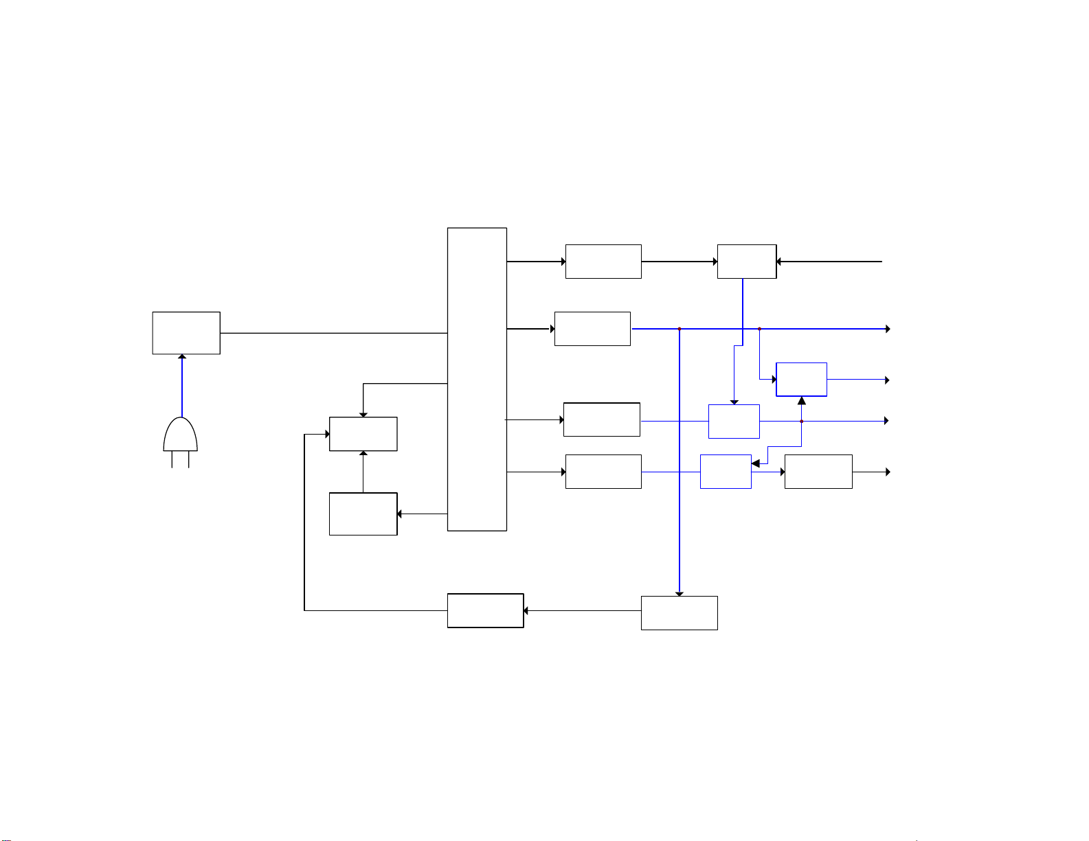
Power Supply Block Diagram
TRANS
D910-913,C901,C902,L901
T901
D906,C912
RECTIFIER
SMOOTHING
Q909,Q905
Power
ON/OFF control
ON/STB
RECTIFIER
SMOOTHING
AC 120V 50/60Hz
Q901
TNY267
CONTROL IC
RECTIFIER
SMOOTHING
D903,C905
PUOTO
CUOPLER
Q902 EL817B
RECTIFIER
SMOOTHING
D904,C907,C908
RECTIFIER
SMOOTHING
D905,C910
RECTIFIER
SMOOTHING
D907,C914
ERROR AMP
Q903 TL431
Q906
ON/OFF SW
Q907,Q908
ON/OFF SW
Q911
ON/OFF SW
VOLTAGE REDUCE
FILTER
ZD901,C909,R911
5VSTB
+5V
+12V
-12V
Page 7
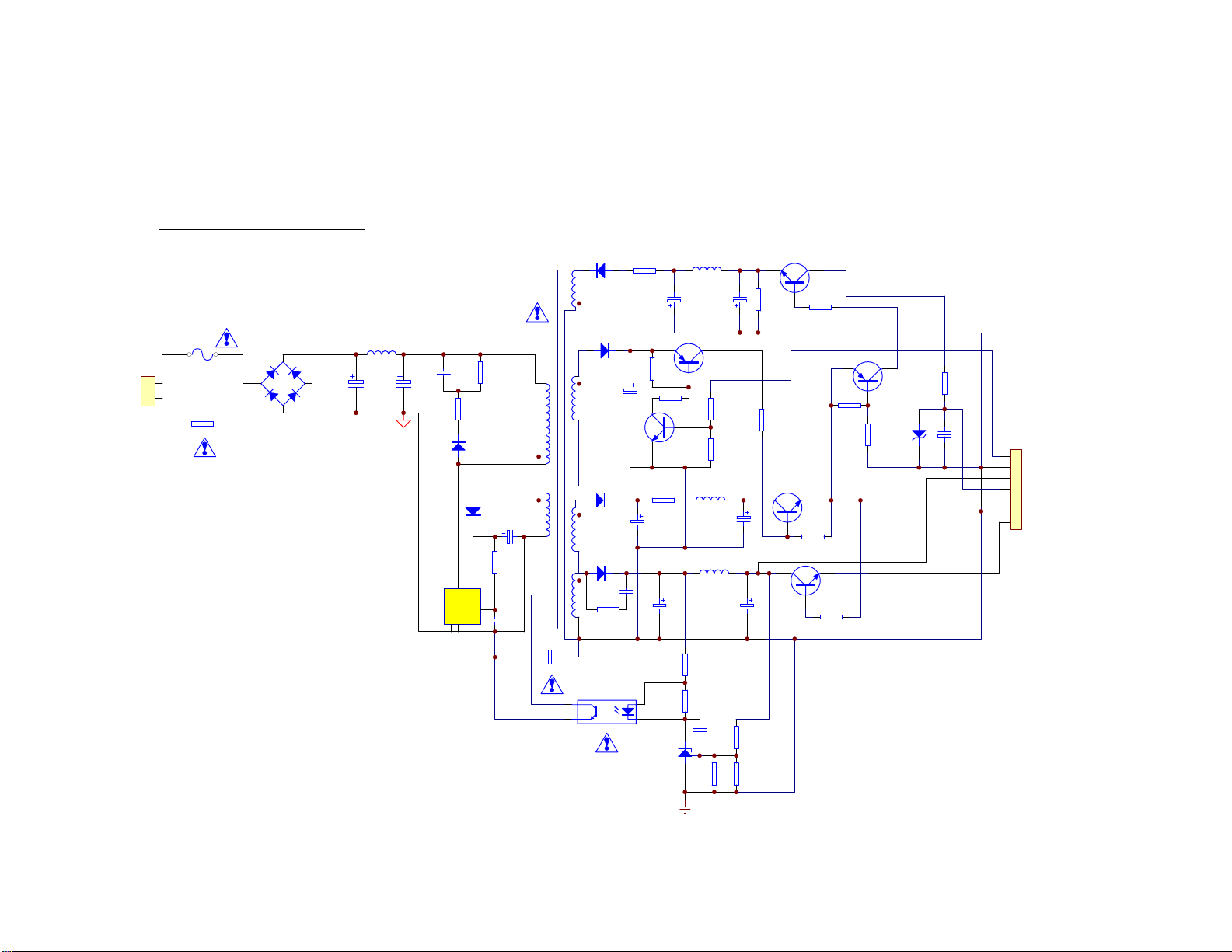
CIRCUIT DIAGRAMS
Power Supply Circuit Diagram
D907
FR104
T901
F901
F1AL/125V
1
2
RH901
10D-9
D910-D913
IN4007
C901
4.7UF/250V
L901
1mH
C902
33UF/250V
C903
D902
R901
2.2nF/1KV
R902
100R-1\4W
1N4007
Q901
TNY267
EN
D
BP
S S S
S
150K/1W
D903
FR104
R903
4.7uF/50V
C905
10K-1\4W
C904
0.1uF
EEL19
C917
2200PF
Q902 EL817B
D906
FR104
D905
FR104
D904
IN5822
C918
102P
R928
10 1/4W
C912
R923
0R
R921
47uF/50V
R924
10R 1/2W
C910
220uF/25V
C907
C914
10K
R914
10K
L902
10uH
47uF/50V
47uF/50V
C911
100uF/25V
C908
R916
R915
470uF/16V
C915
Q909
A9015
R910
1K
Q905
C9014
R912
10K
L903
10uH
L904
5.6uH/2A
1000uF/10V
R905
240R
R904
1K
Q907
S8050
10K
R917
10K
680R/1W
Q908
A9015
1K
R918
10K
R922
10K
R911
12V 500mW
ZD901
C909
100uF/25V
CN902
7
PWON
6
GND
5
Q906
S8050
R913
10K
Q911
C2655
R926
470R 1W
STB5V
4
-12V
3
+12V
2
GND
1
+5V
Q903
AZ431
R907
C906
0.1uF
240K
R908
R906
10K
10K
Page 8
Terminal Voltage Lists
AC IN: 120V 60Hz UNIT : V
Q903 Q905 Q906
KGA
OFF 3.71 2.49
ON 3.73 2.49
PLAY 3.73 2.49
Q908 Q909
ECBECBECB
OFF 12.78 12.75 12.08 17.03 0.01 17.01 5.08 5.09 5.84
ON 12.88 12.84 12.16 17.12 17.08 16.1 5.08 5.09 5.83
PLAY 13.21 13.19 12.5 17.64 17.66 16.94 5.08 5.09 5.83
0 0 16.99
00
00
ECBECBECB
0.07 12.78 12.8 13.51 -26.5 -26.45 -25.76
0.01 0.73 12.78 12.84 13.6 -26.47 -27.15 -26.82
0.01 0.73 13.16 13.22 13.91 -27.91 -16.87 -27.56
Q911
Q907
Page 9
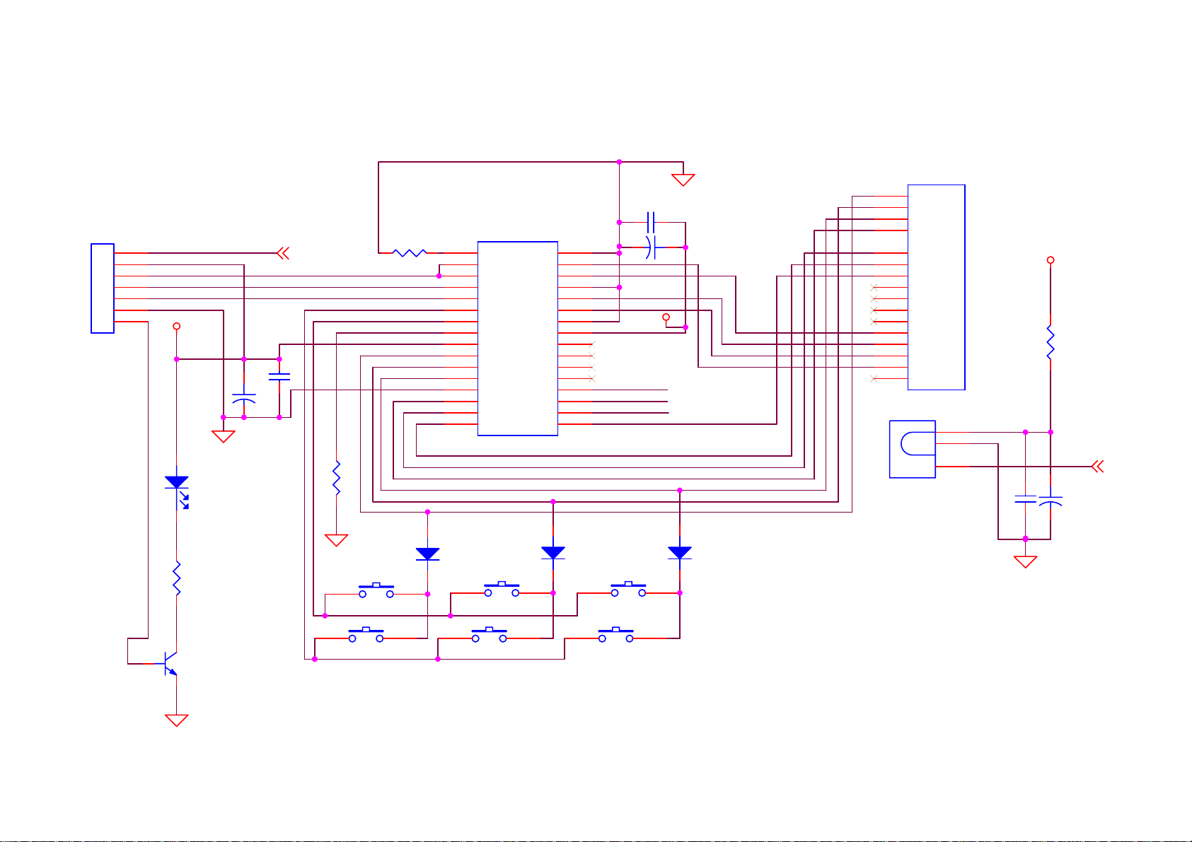
JP1
VCC
DATAIN
CLK
STB
GND
DATA OUT
FRONT DISPLAY CIRCUIT DIAGRAM
R1
1
IR
2
3
4
5
6
VCC
7
100UF
+
TC2
LED1
R3
IR
0.1UF
C2
R2
100
51K
D1
1
2
3
4
5
6
7
8
9
10
11
12
13
14
15
16 17
12
U1
ETK6201
OSC
DOUT
DIN
CLK
STB
K1
K2
K3
VDD
SG1
SG2
SG12
SG3
SG11
NC
SG10
SG4
SG5
SG6 SG7
GND
GR1
GR2
GND
GR3
GR4
GND
VDD
GR5
GR6
SG9
SG8
13
A
15
B
16
12
10
14
11
U2
2
6
5
7
3
9
8
1
4
C
D
E
F
G
DP4
D1D2
NC
NC
DIGIT.2
DIGIT3
DIGIT4
DIGIT.1
DID2-
VCC
U3
1
2
3
R7
22
0.1UF
C3
+
TC3
100UF
IR
0.1UF
C1
TC1
100UF
32
31
30
29
28
27
26
25
24
23
22
21
20
19
18
12
D2
+
VCC
LED4
LED3
LED2
12
D3
Q1
100
2N3904
O/C1
STOP4
FF
SKD2
PLAY5
SKU3
POWER6
Page 10

Main chip & SDRAM CIRCUIT DIAGRAM
TRACK_S TRACK_PWM
TRACK_S
SLED_S
SLED_S
SPINDLE_S
SPINDLE_S
FOCUS_S
FOCUS_S
R171
IRRCV
1K
Adjust R115,Make sure IR signal 3.3V!
MEMCS1-
MEMWR-
MEMDAT[15:0]
MEMRD-
MEMCS0-
MEMADD[19:0]
R121
4.7K
[RD]
1
JP101
BOOTSEL2
[RD]
PCB layout guy: please print this table on PCB silkscreen layer
C170
1nF
FPC_STB/ICEDI
DSPVCC33
2
C104
1nF
IR
MEMADD15
MEMADD16
MEMADD14
MEMADD13
MEMADD12
MEMDAT15
MEMADD11
MEMDAT7
MEMADD10
MEMDAT14
MEMADD9
MEMDAT6
MEMADD8
MEMDAT13
MEMDAT5
MEMDAT12
MEMWRMEMDAT4
MEMDAT11
MEMDAT3
MEMADD19
MEMDAT10
MEMADD18
MEMDAT2
MEMADD17
MEMDAT9
MEMADD7
MEMDAT1
MEMADD6
MEMDAT8
MEMADD5
MEMDAT0
MEMADD4
MEMRDMEMADD3
MEMADD2
MEMCS0MEMADD1
MEMADD0
R122
4.7K
[RD]
JP102
BOOTSEL1
[RD]
1
C105
R115
10K(TBD)
2
1nF
R128 51K(TBD)
R105 30K
R104 15K
R127 43K(TBD)
C101
C102
27nF
27nF
FPC_CLK/ICECLK
FPC_DOUT/ICETDO
U101A
MARK5
.
1
1
FGPCIO0/ADPTDI
2
MEMCS1#/GPCIO18/FCUIF29
3
VDDP
4
MEMADD[15]/FCUIF45
5
MEMADD[16]/FCUIF46
6
MEMADD[14]/FCUIF44
7
MEMADD[13]/FCUIF43
8
MEMADD[12]/FCUIF42
9
MEMDAT[15]/FCUIF28
10
MEMADD[11]/FCUIF41
11
MEMDAT[7]/FCUIF9
12
GNDP
13
MEMADD[10]/FCUIF20
14
MEMDAT[14]/FCUIF27
15
MEMADD[9]/FCUIF19
16
MEMDAT[6]/FCUIF8
17
MEMADD[8]/FCUIF18
18
MEMDAT[13]/FCUIF26
19
MEMDAT[5]/FCUIF7
20
MEMADD[20]/FCUIF50/GPCIO19/MEMCS2#/MEMMSB
21
VDDP
22
MEMDAT[12]/FCUIF25
23
MEMWR#/FCUIF0
24
MEMDAT[4]/FCUIF6
25
VDDC
26
MEMDAT[11]/FCUIF24
27
MEMDAT[3]/FCUIF5
28
MEMADD[19]/FCUIF49
29
GNDC
30
MEMDAT[10]/FCUIF23
31
MEMADD[18]/FCUIF48/BYTEMODE
32
GNDP
33
MEMDAT[2]/FCUIF4
34
MEMADD[17]/FCUIF47/SYSIND2
35
MEMDAT[9]/FCUIF22
36
MEMADD[7]/FCUIF17
37
MEMDAT[1]/FCUIF3
38
MEMADD[6]/FCUIF16
39
MEMDAT[8]/FCUIF21
40
MEMADD[5]/FCUIF15
41
VDDP
42
MEMDAT[0]/FCUIF2
43
MEMADD[4]/FCUIF14
44
MEMRD#/FCUIF1
45
MEMADD[3]/FCUIF13
46
MEMADD[2]/FCUIF12
47
MEMCS#[0]/FCUIF38
48
MEMADD[1]/FCUIF11/BOOTSEL2
49
MEMADD[0]/FCUIF10/BOOTSEL1
50
GNDP
51
VDD-IP
52
VDDP
ZR36882
BOOTSEL
Play OPEN
Download
SLED_PWM
SPINDLE_PWM
FOCUS_PWM
C103
R101
0.1uF
20K 1%
1
RD0
.
1
TD0
.
1
RD1
.
1
.
TD1
208
207
206
205
204
203
GPCIO38/DUPTD1
GPCIO36/DUPTD0
GPCIO37/DUPRD1
FGPICO3/GPCIO16
FGPCIO2/GPCIO47
HOMESW
202
201
200
199
198
197
VDDPWM
GPCIO35/DUPRD0
PWMCO[0]/GPCIO41
PWMCO[5]/GPCIO46
PWMCO[4]/GPCIO45
PWMCO[6]/IDGPCIO4
196
195
194
193
192
191
190
189
GNDP
VDD-IP
GNDPWM
FCUIF34/IDGPCIO7
FCUIF31/IDGPCIO6
FCUIF33/ICGPCIO7
FCUIF30/ICGPCIO6
PWMCO[2]/GPCIO43
PWMCO[3]/GPCIO44/FGPIO1
U101B
209
HOLE1
210
HOLE2
211
HOLE3
212
HOLE4
213
HOLE5
214
HOLE6
215
HOLE7
216
HOLE8
217
HOLE9
218
HOLE10
219
HOLE11
220
HOLE12
OUTSW
INSW
188
187
186
185
184
183
VDDP
GNDC
FCUIF32/GPCIO32
FCUIF36/IDGPCIO3
FCUIF33/ICGPCIO5
FCUIF37/ICGPCIO4
256
257
HOLE48
HOLE49
HOLE13
HOLE14
221
222
182
VDDC
255
HOLE47
HOLE15
223
180
181
GNDADC
253
254
HOLE46
HOLE16
224
225
CD_LD
DVD_LD
178
179
CD_LD
DVD_LD
GNDAFER
251
252
HOLE43
HOLE44
HOLE45
HOLE17
HOLE18
HOLE19
226
227
MD_DVD
176
177
DVD_MD
249
250
HOLE42
HOLE20
228
229
MD_CD
175
CD_MD
248
HOLE41
HOLE21
230
VC
174
173
BGCAP
OPU_REF
RESLOAD
246
247
HOLE38
HOLE39
HOLE40
HOLE22
HOLE23
HOLE24
231
232
RFF
172
F
HOLE25
233
ZR36882
RAMADD[4]
RAMADD[3]
RAMADD[5]
RAMADD[2]
RAMADD[6]
VDDP
RAMADD[1]
RAMADD[7]
RAMADD[0]
GNDP
RAMADD[8]
VDDC
RAMADD[10]
GNDC
RAMADD[9]
VDDP
RAMADD[11]
RAMCS0#0/RAMBA[1]
RAMBA[0]
GNDP
RAMCS1#
RAMRAS#
RAMCAS#
VDDP
RAMWE#
RAMDQM
GNDPCLK
PCLK
VDDPCLK
RAMDAT[8]
GNDP
RAMDAT[7]
RAMDAT[9]
RAMDAT[6]
VDDP
RAMDAT[10]
RAMDAT7
RAMDAT8
VDD_PCLK
R123
56R
C134
0.1uF
RAMDAT6
RAMDAT9
RAMDAT[5]
RAMDAT10
RAMDAT5
PCLK
C106
5pF
C135
0.1uF
5354555657585960616263646566676869707172737475767778798081828384858687888990919293949596979899
RAMADD9
RAMADD10
RAMCS0-
RAMBA
RAMADD11
C131
0.1uF
RAMCS1-
RAMRAS-
C132
0.1uF
RAMCAS-
RAMWE-
RAMDQM
IPCLK
GND_PCLK
C133
0.1uF
JP101
OPEN
CLOSE
RAMADD4
RAMADD3
RAMADD2
RAMADD6
RAMADD5
JP102
OPEN
CLOSE
OPENSW debug
RAMADD0
RAMADD7
RAMADD1
RAMADD8
C130
0.1uF
RFD
RFE
SPDL_SENS+
SPDL_SENS-
170
171
167
168
166
169
E
K
DJC
GND_ADC
245
HOLE37
244
HOLE36
243
HOLE35
242
HOLE34
241
HOLE33
240
HOLE32
239
HOLE31
238
HOLE30
237
HOLE29
236
HOLE28
235
HOLE27
234
HOLE26
VCLKx2/APWM2-/CPUTMS/COSYNC/ICGPCIO1
RAMDAT[11]
GNDP
RAMDAT[4]
VDDC
RAMDAT[12]
RAMDAT12
RAMDAT11
RAMDAT4
C136
0.1uF
RFINN
RFC
RFA
RFB
RFINP
161
163
165
162
159
160
164
158
157
BGA
H
GNDC
RAMDAT3
C163
10nF
RFP
RFN
VDDAFE
VDDAFE
VDDSAFE
GNDDACBS2
DAC2_Y/R/V/C
DAC3_CVBS/C/Y
DAC4_CVBS/G/Y
DAC5_CVBS/C/Y
APWM7-/AOUT5/IDGPCIO2
APWM7+/AOUT4/GPCIO31
VID[0]/APWM6-/ICGPCIO3
VID[1]/APWM6+/GPCIO30
VID[2]/APWM5-/GPCIO29
VID[3]/APWM5+/GPCIO28
VID[4]/APWM4-/ADPTCK/GPIO27
VID[5]/APWM4+/ADPTDO/IDGPCIO1
VID[6]/APWM3-/ADPTDI/ICGPCIO2
VID[7]/APWM3+/ADPTMS//GPCIO26
HSYNC#/CPUTDO/GPCIO25
VSYNC#/CPUTDI/GPCIO24
AIN1/APWM2+/CPUTCK/GPCIO23
ABCLK/GPCIO67
ALRCLK/GPCIO66
SPDIFIN1/AIN2/GPAIO/GPCIO65
AOUT0/APWM1-
AOUT1/APWM1+/GPCIO22
AOUT2/APWM0-/GPCIO21
SPDIFOUT/GPCIO64
SPDIFIN3/IDGPCIO0
AOUT3/APWM0+/ICGPCIO0
RAMCKE/CPUNMI/GPCIO20
RAMDAT[3]
VDDP
RAMDAT[13]
RAMDAT[2]
RAMDAT[14]
GNDP
RAMDAT[1]
RAMDAT[15]
RAMDAT[0]
100
101
102
103
104
RAMDAT13
RAMDAT15
RAMDAT14
RAMDAT2
RAMDAT0
RAMDAT1
FB111
220Z
FB112
MBW2012-221
C138
C137
0.1uF
0.1uF
GNDDACP
RSET
DAC1_C/B/U
VDDDAC
VDDDAC
GNDDAC_D
GNDDAC_D
VDDPLL
RESET#
GNDPLL
GNDP
VDDP
VDDC
GNDC
VDDP
GNDP
VDDP-A2
AMCLK
GNDP-A2
GNDP
VDDP
MARK6
1
CPUNMI
1
JP103
NMI button
[RD]
C139
0.1uF
Note:R127 and R128 value to be determined!!!
<----Operate/Standby
<---- 5mA/0.1mA
VDDPWM
VDDAFE
<----180mA/10mA
<----190mA/0.1mA
LED1
MUTEC
FS1
FS2
FS3
C147
10nF
VDDP
C144
0.1uF
C196
10nF
C148
0.1uF
C145
0.1uF
<---- 7mA/3mA
DSPVCC33
AUDIO_RAUDIO_R+
AUDIO_LSPDIF
AUDIO_L+
C1101nF
C1091nF
RF
VDDDAC
156
155
R106 392R 1%
154
153
152
151
150
149
148
147
146
145
OSCIN
144
XIN
XO
.
2
OSCOUT
143
VDDA
142
141
140
139
138
137
136
135
134
133
132
131
130
129
128
127
126
125
124
123
122
121
120
119
118
117
116
115
114
113
112
111
110
109
108
107
106
105
C140
0.1uF
C141
0.1uF
CD/DVD
CLOSE
OPEN
DRVSB
Z109
C146
10nF
R119
4.7K
C143
0.1uF
C119
0.1uF
C121
0.1uF
C123
0.1uF
C116
0.1uF
C149
0.1uF
C164
1nF
+
C159
47uF/16V
+
C120
100uF/16V
MBW2012-221
+
C122
100uF/16V
MBW2012-221
C124
+
100uF/16V
C117
+
100uF/16V
+
VDDP
R184
0R
C150
0.1uF
FB105
MBW2012-221
FB102
220Z
FB101
FB104
FB103
220Z
R120
4.7K
C108
22uF/16V
VDD_A2
R185
1K
FB120
MBW2012-221
C199
1nF
C151
+
220uF/16V
231
C125
10nF
RAMCKE
C160
1nF
DSPVCC18
DSPVCC33
DSPVCC33
DSPVCC18
R130
10R
[RD]
FB115
MBW2012-221
STBY
C113
2.7uH
220pF
C114
22pF
3rd overtone crystal
C115
22pF
Use PH1 to connect the shell of the crystal with net GND.
R108
R133
75R 1%
75R 1%
D101
BAT54S
RESET-
JP105
2
1
RESET BUTTON
[RD]
DSPVCC33
RAMDAT15
RAMDAT14
54
VSS
DQ15
DQ14
VSSQ
U104
VDD
DQ0
VDDQ
DQ1
123456789101112131415161718192021222324252627 28
RAMDAT0
RAMDAT1
C158
+
47uF/16V
L102
R109
75R 1%
RAMDAT13RAMDAT2
RAMDAT12
DQ13
VDDQ
DQ2
VSSQ
RAMDAT3
SDRAMVCC33
1
RAMDAT11
DQ11
DQ12
DQ3
DQ4
RAMDAT4
TP36
.
TP35
.
1
1
Y101
27.000MHz
R129
R112
33R
220K
PH1
.
R110
R111
75R 1%
75R 1%
PCLK
RAMDQM
RAMDAT9
RAMDAT8
RAMDAT10
NC
VSS
DQ8
DQ9
DQ10
VSSQ
VDDQ
DQMH
HY57V641620E
VDDQ
DQ5
DQ6
VSSQ
DQ7
VDD
DQML
WE#
RAMDQM
RAMDAT5
RAMDAT7
RAMCAS-
RAMWE-
RAMDAT6
SDRAM speed <=7ns
C153
C152
10nF
10nF
R113
33R
RAMCKE
CLK
CKE
CAS#
RAS#
RAMCS1-
RAMRAS-
C154
0.1uF
OSCOUT
C_B_U
Y_R_V
CVBS_C
CVBS_G_Y
Y/C
RAMADD9
RAMADD11
A9
NC
A11
CS#
BA0
BA1
RAMCS0-
RAMBA
OSCIN
RAMADD7
RAMADD8RAMADD10
RAMADD6
A10A0A1A2A3
RAMADD0
RAMADD1
C156
0.1uF
RAMADD4
RAMADD5
29303132333435363738394041424344454647484950515253
A4A5A6A7A8
RAMADD3
RAMADD2
VDD VSS
FB106
DSPVCC33
220Z
C157
0.1uF
Page 11

POWER & AV OUTPT CIRCUIT DIAGRAM
TP33
TP34
TP31
TP32
.
.
.
1
1
1
CN501
1
2
3
4
5
6
7
8
9
10
11
SCART Port
FOR D2 TERMINAL
R5002,R510,R5006 NM
R5001,R511,R516 0R
R509,R514 3.3K
R5004 2.2K
R512,R513 4.7K
R5003 8.2K
SCART/D2 TERMINAL circuit
DATAIN
DATA OUT
Power supply board should
cut off D5V, M5V, +12V & -12V
when STBY (RAMCKE) = LOW
TP1
TP2
TP3
TP6
TP4
TP5
.
.
.
.
.
1
1
1
1
1
+12V: +12V(+-10%)
-12V: -12V(+-10%)
+5V: +5V(+-2.5%)
TP27
TP28
TP29
TP30
.
.
.
.
1
1
1
1
1
CVBS_OUT
G-Y_OUT
C-B-U_OUT
Y-R-V_OUT
SCART_SWITCH/D_VFORMART
AUDIO/TV/16:9/D_SPEC
RMAIN-OUT
LMAIN-OUT
FP_IR
1
IR
FP_5V
2
VCC
FP_DAT
3
FP_CLK
4
CLK
FP_STB
5
STB
6
GND
7
CN504
.
1
+5V
1
2
GND
3
+12V
4
-12V
5
5VSTB
6
GND
7
PW-ON
POWER
TP24
TP25
TP26
.
.
.
.
1
1
1
FS1: H=RGB L=CVBS
FS2 FS3
00
01
10
FS2
FS3
6.8KR5005
FS1
DEFAULT FOR SCART
TP13
.
TP12
.
1
TP11
.
1
TP10
.
1
TP9
.
1
TP8
.
1
TP7
.
1
1
C534
C535
1nF
100pF
SW5V
FB502 MBW2012-221
P12V
FB503 220Z
N12V
FB504 220Z
ST5V
FB510 MBW2012-221
STBY
C161
1nF
SCART CFG
C531
100pF
C568
0.1uF
4:3
TV
16:9
C532
100pF
C569
0.1uF
R512
10K
R513
10K
R515
4.7K
C533
100pF
C570
0.1uF
R5002
1
C512
1nF
D5V+12V
0R
R509
2K
R511
1K
Q501
BT3904
2 3
1
FB509 220Z
R540 220R
R541 220R
R542 220R
R543 220R
R546 4.7K
C571
0.1uF
2 3
C572
0.1uF
R5001
[0R]
R510
2K
R5004
0R
Q502
BT3904
BT3904
NM
R5003 0R
D5V
Q503
1
R516
1K
C541
100pF
STBY5V
2 3
AUDIO/TV/16:9/D_SPEC
Video Status
R514
150R
R5005
NM [0R]
R5006
NM
SCART_SWITCH/D_VFORMART
[0R]
STBY5V
R501
R503
R502
10K
10K
10K
D5V
+
+
C503
C502
100uF/16V
220uF/10V
RGB Status
R504
4.7K
IRRCV
FPC_DOUT/ICETDO
FPC_CLK/ICECLK
FPC_STB/ICEDI
LED1
RFA5V
+12V
-12V
M5V
RFA5V
D5V
+12V
-12V
M5V
CVBS_C
Y_R_V
CVBS_G_Y
C_B_U
C520 11pF
CVBS_C
L501 1.1uH
C511
150pF
C522 11pF
Y_R_V
L502 1.1uH
C514
150pF
C524 11pF
CVBS_G_Y
L503 1.1uH
C513
150pF
C526 11pF
C_B_U
L504 1.1uH
C515
150pF
C517 11pF
Y/C
L505 1.1uH
C516
150pF
Close to Q505
SPDIF
Q505
SPDIF
1
BT3904
2 3
R529
56R
R544
62R
R530
39R
C509
0.1uF
C528
0.1uF
FB505 MBW2012-221
C521
160pF
BAT54S
FB506 MBW2012-221
C523
160pF
BAT54S
FB507 MBW2012-221
C525
160pF
BAT54S
FB508 MBW2012-221
BAT54S
C527
160pF
FB511 MBW2012-221
C518
160pF
BAT54S
D5V
COAX_SPDIF
C510
22pF
D501
D502
D503
D504
D505
231
231
231
231
+
C529
220uF/10V
Y/C_OUT
231
ESD2V
C-B-U_OUT
Y/C_OUT
ESD2V
C530
0.1uF
RMAIN-OUT
R532
330R
LMAIN-OUT
R521
0R
R522
NM
[0R]
CVBS_OUT
Y-R-V_OUT
G-Y_OUT
C-B-U_OUT
R533
220R
TP42
.
1
Y-R-V_OUT
CVBS_OUT
C-B-U_OUT
G-Y_OUT
C540
1nF
TP40
TP41
TP44
AVCC33
TP37
.
1
.
1
.
1
1
.
TP39
.
1
TP38
.
1
C539
1nF
TP43
Q510 NM
2 3
15
12
16
11
17
10
5
8
4
.
1
1
JR502B
15
12
16
11
17
10
5
8
4
Digital
S-VIDEO
R5080R
DSPVCC33
R545
D5V
NM
3
3
2
2
1
1
A-JACK-2X3
9
6
7
9
6
7
R523
0R
R524
NM
[0R]
COAX_SPDIF
Y-R-V_OUT
CVBS_OUT
TP45
.
1
Y
R
H1
3 4
34
2
2
5
1
1
9
678
9
678
H1
MARK1
1
MARK2
1
MARK3
1
MARK4
1
H2
3 4
2
5
1
PbCoaxial
L
.
.
.
.
34
2
5
1
678
9
H2
678
9
Pr
CVBS
5
Page 12

FE & DRIVER CIRCUIT DIAGRAM
DSPVCC33
R221
1R
1
R224
1R
1
VC
PDIC_SEL
1
.
1
TP58
.
TP51
C212
0.1uF
2.1V
1
.
1
TP48
.
TP50
MD_CD
MD_DVD
CD/DVD
+
+
1
.
TP47
C228
47uF/16V
R222
220R
C229
47uF/16V
R223
220R
1
.
R202
0R
RFE
VC
RFF
RFB
RFA
RF
RFD
RFC
DVD_LD
CD_LD
TP64
C202
0.1uF
1
.
TP23
1
.
TP22
RFA5V
+
C201
100uF/16V
TP19
TP21
.
.
TP18
TP20
.
.
.
1
1
1
1
1
OPU S75
connector
CN201
24Pin OPU connector
GND-LD
DVD-LD
NC
HFM
MD
CD-LD
VR-DVD
VR-CD
NC
E
VCC
VC(VREF)
GND/PD
F
B
A
RF
CD/DVD_SW
D
C
TT+
F+
F-
GND
GND
25
26
VR_DVD
VR_CD
PDIC_SEL
23
Q212
BT3904
24
23
22
21
20
19
18
17
16
15
14
13
12
11
10
9
8
7
6
5
4
3
2
1
TP49
R270
0R
1
1
OPU5V
VREF
TACTTACT+
FACT+
FACT-
.
TP56
R280
3.3K
.
1
Q201
BT3904
TP52
C207
0.1uF
C203
0.1uF
TP46
RFA5V
1
TP57
1
2 3
C205
C231
+
100uF/16V
0.1uF
23
TP54
TP55
.
.
.
1
1
C208
0.1uF
DVDLD
CDLD
VR_DVD
.
VR_CD
1
RF
C204
0.1uF
.
TP62
R278
R208
0R
470R
23
Q213
BT3904
1
BT2907
TP53
.
1
TP63
BT2907
OPU_HFM
L201 10uH
R217 33R
1
.
TP65
C209
+
47uF/16V
1
.
R249
1
3.3K
R235
3.3K
Q204
.
1
Q205
TP61
23
1
.
1
.
TP59
TP60
TP17
.
TP16
1
DSPVCC33
R264
R9278
1K 1%
R265
1K 1%
M5V
R298
NM
C274
NM
33K
C246
0.1uF
U202
R236
10K
C214
1nF
A5888
1
VINFC
2
TRB 1
3
REGO 2
4
VINSL+
5
REGO 1
6
FWD
7
REV
8
VCC1
9
VOTR-
10
VOTR+
11
VOSL+
12
VOSL-
13
VOFC-
14
VOFC+
GND
GND
29
30
R237
10K
HOMESW
OUTSW
INSW
C215
1nF
M5V
12
D201
1N4001
R218
1.2K/1%
1
R219
2K/1%
23
Q210
S8550
3V3_DRV
DSPVCC33
3V3_FB
C276
+
220uF
STBY
BIAS
VINTK
TRB 2
VINLD
GND
VCTL
VCC2
VOLD-
VOLD+
VOTK-
VOTK+
28
27
R268 0R
26
1V8_DRV
25
24
NC
23
22
21
20
NC
19
18
17
16
15
1V8_DRV
C220
0.1uF
1V8_FB
+
LOADLOAD+
SLED+
SLED-
HOMESW
LOAD+
LOAD-
OUTSW
INSW
C244
220uF/10V
GND
SP+
SP-
GND
R243
0R
1
2
3
4
5
6
7
8
9
10
11
3V3_DRV
1V8_FB
3V3_FB
C245
0.1uF
R254
10K
C213
1nF
SLEDSLED+
HOMESW
SP+
SPLOAD+
LOADOUTSW
INSW
DSPVCC33
FOCUS_S
SLED_S
CLOSE
OPEN
M5V
SLED+
SLED-
FACT+
SP+
SP-
HOMESW
OUTSW
INSW
TP15
.
TP14
.
.
1
1
1
CN203
DRIVE CON
M5V
TACT-FACT-
TACT+
1
M5V
23
VC2
R281
4.7R 2W
Q211
S8550
R220
430/1%
R238
1K/1%
DRVSB
TRACK_S
SPINDLE_S
DSPVCC18
R239
1R
R9249
1K
R260
1K
#2 BEMF circuit
D204
3
NM
SPDL_SENS+
R276
NM
C242
0.1uF
M5V
1
R277
NM
R299
NM
NM
DSPVCC33
R600
R263
1K
SPDL_SENS+
R9280
4.7K
R279
NM
R203
NM
SPDL_SENSSPDL_SENS+
84
U206A
3
+
2
-
LM358
C251
NM
2
1
Page 13

FLASH & SRAM I/F CIRCUIT DIAGRAM
Flash speed <= 70 nS.
If plan to use 90ns Flash, it needs to be verified by s/w.
MEMDAT[15:0]
MEMADD[19:0]
U106
1
A15
2
3
4
5
6
7
8
9
10
11
12
13
14
15
16
17
18
19
20
21
22
23
24
A14
A13
A12
A11
A10
A9
A8
NC
NC
WE#
RP#
VPP
WP#
A19
A18
A17
A7
A6
A5
A4
A3
A2
A1
(BYTE#)
(A19)
(NC)
(NC)
(RY/BY#)
SST39VF800A
MEMCS0-
MEMCS1-
Pin10 of U106: A20 -->NC
RESET-
Selector for
16Mb Flash
R160 R161
Intel NM 0R
AMD/SST 0R NM
MEMRD-
MEMWR-
MEMRD-
MEMWR-
MEMADD19
R160 0R
R161 NM
[0R]
MEMADD15
MEMADD14
MEMADD13
MEMADD12
MEMADD11
MEMADD10
MEMADD9
MEMADD8
INTEL_ADD19
MEMWR-
AMD_ADD19
MEMADD18
MEMADD17
MEMADD7
MEMADD6
MEMADD5
MEMADD4
MEMADD3
MEMADD2
MEMADD1
C162
NM
[0R]
0.1uF
SSRAMCS-
MEMADD16
48
A16
47
VCCQ
46
GND
DQ15
DQ7
DQ14
DQ6
DQ13
DQ5
DQ12
DQ4
VCC
DQ11
DQ3
DQ10
DQ2
DQ9
DQ1
DQ8
DQ0
OE#
GND
CE#
A0
MEMCS0- FLASHCS-
MEMCS1-
MEMDAT15
45
MEMDAT7
44
MEMDAT14
43
MEMDAT6
42
MEMDAT13
41
MEMDAT5
40
MEMDAT12
39
MEMDAT4
38
37
MEMDAT11
36
MEMDAT3
35
MEMDAT10
34
MEMDAT2
33
MEMDAT9
32
MEMDAT1
31
MEMDAT8
30
MEMDAT0
29
MEMRD-
28
27
FLASHCS-
26
MEMADD0
25
R164
JP104
3
1
4
2
FOR DEBUG
[RD]
JP104 Mem. select
Flash
SRAM
1-3
1-2
3-4
DSPVCC33
Close to Pin37 of U106
DSPVCC33
R168
R165
4.7K
4.7K
R&D MP
JP104
R164
R165
JUMPER NM
NM
4.7K NM
0R
1301
DSPVCC33
1
DSPVCC33
2
GND
3
SSRAMCS-
4
MEMADD0
5
MEMRD-
6
MEMDAT0
7
MEMDAT8
8
MEMDAT1
9
MEMDAT9
10
MEMDAT2
11
MEMDAT10
12
MEMDAT3
13
MEMDAT11
14
MEMDAT4
15
MEMDAT12
16
MEMDAT5
17
MEMDAT13
18
MEMDAT6
19
MEMDAT14
20
MEMDAT7
21
MEMDAT15
22
GND
23
GND
24
MEMADD16
25
MEMADD19
26
MEMADD1
27
MEMADD2
28
MEMADD3
29
MEMADD4
30
MEMADD5
31
MEMADD6
32
MEMADD7
33
MEMADD17
34
MEMADD18
35
MEMWR-
36
MEMADD8
37
MEMADD9
38
MEMADD10
39
MEMADD11
40
MEMADD12
41
MEMADD13
42
MEMADD14
43
MEMADD15
44
GND
45
46
47
NM
EXTERNAL SRAM PORT
PCB layout guy: please print this table on PCB silkscreen layer
Page 14

AUDIO CIRCUIT DIAGRAM
Choose the values in "[ ]" when using exter nal a udio D AC
AUDIO_L-
AUDIO_L+
AUDIO_R-
AUDIO_R+
MUTEC
R330 4.75K 1%
R336 4.75K 1%
R343 4.75K 1%
R348 4.75K 1%
R383
47K
R331
4.75K 1%
C326
200pF
R337
4.75K 1%
R344
4.75K 1%
C337
200pF
R349
4.75K 1%
1
R377
4.7K
Q303
BT3904
2 3
RLS4148
1 2
D5V+12V
D302
R332
4.75K 1%
C325
180pF
R338
4.75K 1%
C328
33pF 5%
R345
4.75K 1%
C336
180pF
R350
4.75K 1%
C339
33pF 5%
+
D301 RLS4148
1 2
R390 100K
R392 10K
R399
47K
R378
4.7K
C361
10uF/16V
MUTE_HAND
R3391
118K 1%
R3511
118K 1%
C370
220uF/10V
R3392
118K 1%
R3512
118K 1%
Q304
BT3906
2 3
1
Q307 BT3906
2 3
1
R400
2K
+
C373
47uF/25V
R3332 118K 1%
R3331 118K 1%
R333 118K 1%
C324 33pF 5%
U302A
-
UTC4558
2
+
3
8 4
R339
118K 1%
R3462 118K 1%
R3461 118K 1%
R346 118K 1%
C334 33pF 5%
-
6
+
5
U302B
UTC4558
8 4
R351
118K 1%
MUTE MUTE
1
7
C329
0.1uF
A+12V
R306 2.4K 5%
R318 2.4K 5%
-12V
0.1uF
C335
R322
100K
R323
100K
R340
1.6K 5%
A-12V
R352
1.6K 5%
MUTE
MUTE
A-12V
A+12V
R341
2K
R301
2K
+
1
1
C378
+
47uF/25V
C380
47uF/25V
2 3
2 3
Q317
BT3904
Q318
BT3904
R406
33R
R413
33R
LMAIN-OUT
RMAIN-OUT
-12V
+12V
Page 15

POWER PC BOARD (TOP SIDE)
Page 16

Page 17

Page 18

Page 19

Page 20

POWER IC Q901 TNY267PN
IC BLOCK DIAGRAMS
BYPASS
(BP)
240 µA 50 µA
ENABLE
1.0 V + V
ENABLE/
UNDER-
VOLTAGE
(EN/UV)
1.0 V
DRAIN
REGULATOR
5.8 V
LINE UNDER-VOLTAGE
FAULT
RESET
MAX
PRESENT
CURRENT
LIMIT STATE
MACHINE
5.8 V
4.8 V
THERMAL
SHUTDOWN
SRQ
Q
AUTO-
RESTART
COUNTER
6.3 V
JITTER
CLOCK
T
DC
OSCILLATOR
BYPASS PIN
UNDER-VOLTAGE
+
-
V
I
LIMIT
CURRENT LIMIT
COMPARATOR
LEADING
EDGE
BLANKING
-
+
(D)
U302 UTC4558F
1
-IN1
2
3
45
VEE
1ch
-
8OUT1
VCC
OUT2
+
2ch
+
7
6
-
-IN2+IN1
+IN2
Q903 TL431
Q902 EL817B/BPC-817
1OUT
1
ANODE
1
4
COLLECTOR
1IN-
2
K
G
A
U206 LM358
SOURCE
(S)
VCC+
8
7
2OUT
CATHODE
23
EMITTER
VCC-/GND
3
1IN+
45
6
2IN-
2IN+
Page 21

SDRAM IC U104 HY57V641620E
CLK
CKE
CS
RAS
CAS
WE
U/LDQM
Self refresh
logic & timer
Row Active
State Machine Address Buffers
Refresh
Column Active
Bank Select
Internal Row
Counter
Row
Pre
Decoder
Column
Pre
Decoder
Column Add
Counter
1Mx16 BANK 3
X-Decoder
X-Decoder
X-Decoder
1Mx16 BANK 2
1Mx16 BANK 1
1Mx16 BANK 0
X-Decoder
Memory
Cell
Array
Y-Decoder
Sense AMP & I/O Gate
DQ0
I/O Buffer & Logic
DQ15
A0
A1
A11
BA1
BA0
Address
Register
Mode Register
Burst
Counter
CAS Latency
Pipe Line
Data Out Control
Control
Page 22

SG1/KS1
SG2/KS2
SG3/KS3
SG4/KS4
SG5/KS5
SG6/KS6
SG7/KS7
SG8/KS8
SG9/KS9
SG10/KS10
Dimming Circuit
K1
K2
K3
VDD
GND
FRONT Drive IC U1 ETK6201
DOUT
OSC
DIN
CLK
STB
GND
Control
Serial
Data
Interface
OSC
R
Display Memory
Timing Generator
Key Matrix
Memory
SEGMENT DRIVER/
KEY SCAN OUTPUT/
GRID DRIVER
SG11
SG12/GR7
GR6
GR5
GR4
GR3
GR2
GR1
Page 23

DRIVER IC U202 A5888
FLASH IC U106 SST39VF800A
X-Decoder
Memory Address
Address Buffer & Latches
CE#
OE#
WE#
Control Logic
SuperFlash
Memory
Y-Decoder
I/O Buffers and Data Latches
DQ15 - DQ
0
Page 24

T
A
MPEG IC U101 ZR36882 CHIP
V
FOCUS
OPU
SLEDS
SPIND
TRAY
LOAD
COAX
SPDIF INPUT
SPDIF OUTPUT
SLEDS
SPINDLE
RACK
LOAD
IR RC
Serial Cards
RECEIVER
ZR36882ELCG
FCU
SERVO
AFE
ADP
Audio
ML
CPU
CGU
MCU
USB
VPU
FRONT PANEL
CONCENTRATOR
MP
16Mbits NOR
27M Crystal
RESET
64Mbit SDRAM
TV Monotor(
IDEO
S-VIDEO YUV
ADC DAC
Page 25

PARTS LIST
p
is fulfilled via product exchange.
In-Warranty service for the SD-3990SU, and SD-3990SC DVD Player
Contact Toshiba Customer Solutions for instructions. 1-866-583-7353.
IN-WARRANTY SERVICE
LOCATION
No.
TSB P/N Reference No. Description
AH910002
AH970001 TWR115000XX AV-CABLE L=1500mm
AH930012
AH930015
TSDAC20003A
TSDAC10015A OWNER'S MANUAL OF ENGLISH
TSDAC10016A OWNER'S MANUAL OF FRENCH ( For SC Version )
REMOTE CONTROLLER,SE-R0213 (OET)
SAFETY PRECAUTION
The parts identified by mark are critical for safety. Replace only with part number specified.
The mounting position of replacement is to be identical with originals. The substitute replacement
arts which do not have the same safety characteristics as specified in the parts list may create
shock, fire or other hazards.
Page 26

PARTS LIST
No.
MAIN UNIT
1 AH970065 TSDMT10009A CHASSIS ZINKOTE21 or suitable one t=0.6mm
2 AH940006 TSDMT10011A TOP COVER ZINKOTE21 or suitable one t=0.6mm
3 AH910003 TSDAS20007A MECHA ASS'Y FOR SD-3990
4 AH910004 TAS000018XX MAIN UNIT ASSEMBLY OF SD-3990-S-TU
5 AH920025 TAS000019XX POWER UNIT SD-3990
* 6 AH940007 TSDMT10010A REAR PANEL ZINKOTE21 or suitable one t=0.6mm
7 AH970066 TSDMT20004A FRONT BRACKET ZINKOTE21 or suitable onet=1.0mm
8 AH910005 TAS000017XX FRONT UNIT ASSEMBLY OF SD-3990
9 AH970067 TSDNM30008A POWER BUTTON
10 AH970068 TSDNM30007A FUNCTION BUTTON
11 AH970069 TSDNM20016A POWER INDICATOR
12 AH970070 TSDMT80002A SPRING-DVD DOOR
13 AH920026 TSDNM10005A FRONT PANEL PS (VH-1821)(94V2)
14 AH970071 TSDNM20017A DVD-DOOR ABS(PA-757, 94HB) or suitable one
15 AH970072 TSDNM20013A WINDOW
16 AH970073 TSDNM40001A FOOT CUSHION
17 AH970074 TSDNM40005A MECHA CUSHION(L*W*H=33*8*2.0mm)
TSB P/N Reference No.
Description
DVD MECHANISM
18 AH970075 TSDAS20007B-1 Clamper Plate
19 AH970076 TSDAS20007B-2 Magnet
20 AH970077 TSDAS20007B-3 Clamper Holder
21 AH980029 TSDAS20007B-4 Screw 2.6*8
22 AH970078 TSDAS20007B-5 Clamper
23 AH970091 TSDAS20007B-6 EVA
24 AH970079 TSDAS20007B-7 Chassis
25 AH970080 TSDAS20007B-8 PU Holder
26 AH980028 TSDAS20007B-9 Screw 2.5*9PWA
27 AH970081 TSDAS20007B-10 Deck
28 AH970082 TSDAS20007B-11 Damper
29 AH980030 TSDAS20007B-12 Screw 2.5*9PWA
30 AH970083 TSDAS20007B-13 Connector
31 AH980031 TSDAS20007B-14 Screw 2.5*5PB
32 AH920027 TSDAS20007B-15 PCB
33 AH970084 TSDAS20007B-16 Switch
34 AH980032 TSDAS20007B-17 Motor
35 AH970085 TSDAS20007B-18 Motor Pulley
36 AH970086 TSDAS20007B-19 Tray
37 AH970087 TSDAS20007B-20 Slide
38 AH980033 TSDAS20007B-21
39 AH970088 TSDAS20007B-22 M gear
40 AH980034 TSDAS20007B-23
41 AH970088 TSDAS20007B-24 Belt Gear
42 AH970090 TSDAS20007B-25 Belt
43 AH980035 TSDAS20007B-26
Screw M1.7*3.2
Screw 1.7*6PWA
Screw 1.7*6PWA
* Note: Rear Panel is not service available due to attached rating label.
Page 27

Page 28

Page 29

SpecificationsSpecifications
DVD Video player/outputs/supplied accessories
DVD Video player
Power supply 120 V AC, 60 Hz
Power consumption 13 W
Mass 1.6 kg
External dimensions 430 x 42 x 198 mm (W/H/D)
Signal system Standard NTSC
Laser Semiconductor laser, wavelength 650/780 nm
Frequency range DVD linear sound : 48 kHz sampling 4 Hz to 22 kHz
Signal-to-noise ratio More than 100 dB
Audio dynamic range More than 93 dB
Harmonic distortion Less than -70dB
Wow and flutter Below measurable level (less than ±0.001 % (W.PEAK))
Operating conditions Temperature: 5 °C to 35 °C, Operation status: Horizontal
Outputs
Video
output 1.0 V (p-p), 75 Ω, negative sync., pin jack x 1
S video output (Y) 1.0 V (p-p), 75 Ω, negative sync., Mini DIN 4-pin x 1
Component video output (Y) 1.0 V (p-p), 75 Ω, negative sync., pin jack x 1
Audio output (COAXIAL DIGITAL) 0.5V (p-p), 75 Ω, pin jack x 1
Audio output (ANALOG) 2.0 V (rms), 680 Ω, pin jacks (L, R) x 1
Supplied Accessories
0.286 V (p-p), 75 Ω
(C)
(P
)/(PR) 0.7 V (p-p), 75 Ω, pin jack x 2
B
96
kHz sampling 4 Hz to 44 kHz
Audio/video cable .............................................................................................. 1
Remote control (SE-R0213) .............................................................................. 1
Batteries (AAA) ................................................................................................. 2
• This model complies with the above specifications.
• Designs and specifications are subject to change without notic
• This model may not be compatible with features and/or specifications that may be added in the future.
e.
Page 30

1-1, SHIBAURA 1-CHOME, MINATO- KU, TOKYO 105-8001, JAPAN
 Loading...