Toshiba SD-2800 Service manual
SERVICE MANUAL
DVD VIDEO PLAYER
FILE NO. 810-200201
SD-2800
Mar., 2002
S
SECTION 3
SERVICING DIAGRAMS
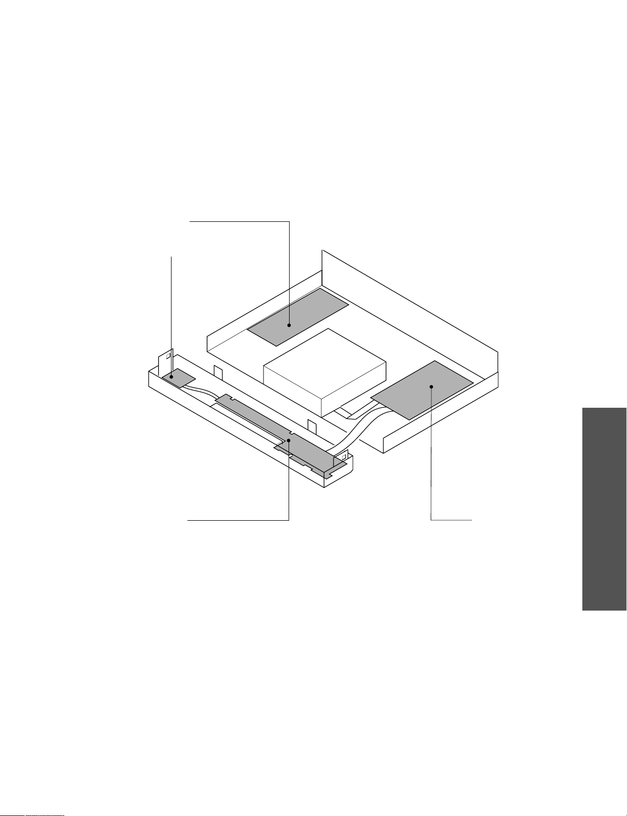
1. STANDING PC BOARDS FOR SERVICING
EU02 Power supply PC board
EU04 Power SW PC board
EU03 Front display PC board
SERVICING DIAGRAMS
SECTION 3
EU01 Main PC board
Fig. 3-1-1
2. CIRCUIT SYMBOLS AND SUPPLEMENTARY EXPLANATION
+
NP
104
10x10
4
pF (0.1mF)
Temperature characteristic
(or Temperature characteristic+
Static electricity capacity tolerance)
2-1. Precautions for Part Replacement
• In the schematic diagram, parts marked (ex.
F801) are critical part to meet the safety regulations,
so always use the parts bearing specified part codes
(SN) when replacing them.
2-2. Solid Resistor Indication
Unit None ........... W
K ........... kW
M ........... MW
Tolerance None ........... ±5%
B ........... ±0.1%
C ........... ±0.25%
D ........... ±0.5%
F ........... ±1%
G ........... ±2%
K ........... ±10%
M ........... ±20%
Rated Wattage (1) Chip Parts
None ......... 1/16W
(2) Other Parts
None ......... 1/6W
Other than above, described in the Circuit Diagram.
Type None ........... Carbon film
S ........... Solid
R ........... Oxide metal film
W ...........Metal film
W ...........Cement
FR ........... Fusible
• Using the parts other than those specified shall violate
the regulations, and may cause troubles such as
operation failures, fire etc.
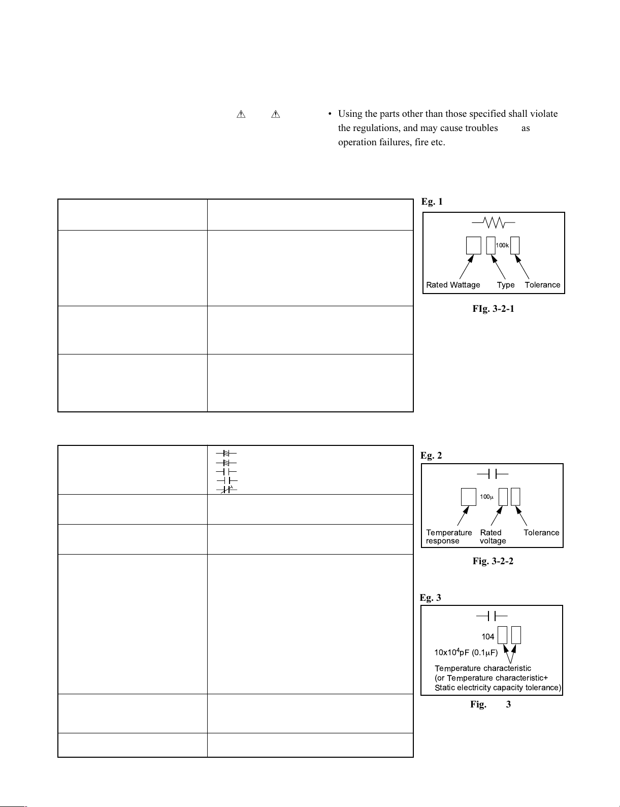
Eg. 1
100k
Rated Wattage Type Tolerance
FIg. 3-2-1
2-3. Capacitance Indication
Symbol
Unit None ........... F
Rated voltage None ........... 50V
Tolerance (1) Ceramic, plastic, and film capacitors of which
Temperature characteristic None ........... SL
(Ceramic capacitor) For others, temperature characteristics are
Static electricity capacity Sometimes described with abbreviated letters as
(Ceramic capacitor) shown in Eg. 3.
........... Electrolytic, Special electrolytic
........... Non polarity electrolytic
........... Ceramic, plastic
M
........... Film
........... Trimmer
m ........... mF
p ........... pF
For other than 50V and electrolytic capacitors,
described in the Circuit Diagram.
capacitance are more than 10 pF.
None ........... ±5% or more
B ........... ±0.1%
C ........... ±0.25%
D ........... ±0.5%
F ........... ±1%
G ........... ±2%
(2) Ceramic, plastic, and film capacitors of which
capacitance are 10 pF or less.
None ........... more than ±5% pF
B ........... ±0.1 pF
C ........... ±0.25 pF
(3) Electrolytic, Trimmer
Tolerance is not described.
described. (For capacitors of 0.01 mF and
no indications are described as F.)
Eg. 2
Temperature
response
Eg. 3
100
m
Rated
voltage
Fig. 3-2-2
Fig. 3-2-3
Tolerance
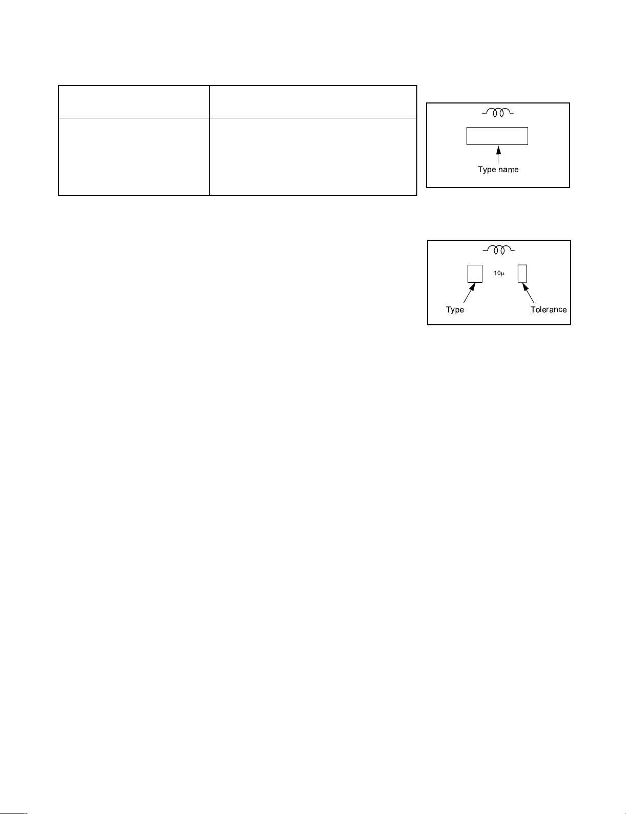
2-4. Inductor Indication
Type name
10
m
Type Tolerance
Unit None ........... H
m ........... mH
m ...........mH
Tolerance None ........... ±5%
B ........... ±0.1%
C ........... ±0.25%
D ........... ±0.5%
F ........... ±1%
G ........... ±2%
K ........... ±10%
M ........... ±20%
2-5. Waveform and Voltage Measurement
• The waveforms for CD/DVD and RF shown in the
circuit diagrams are obtained when a test disc is
played back.
• All voltage values except the waveforms are expressed
in DC and measured by a digital voltmeter.
2-6. Others
• The parts indicated with "NC" or "KETU" etc. are not
used in the circuits of this model.
Eg. 4
Fig. 3-2-4
Eg. 5
Fig. 3-2-5
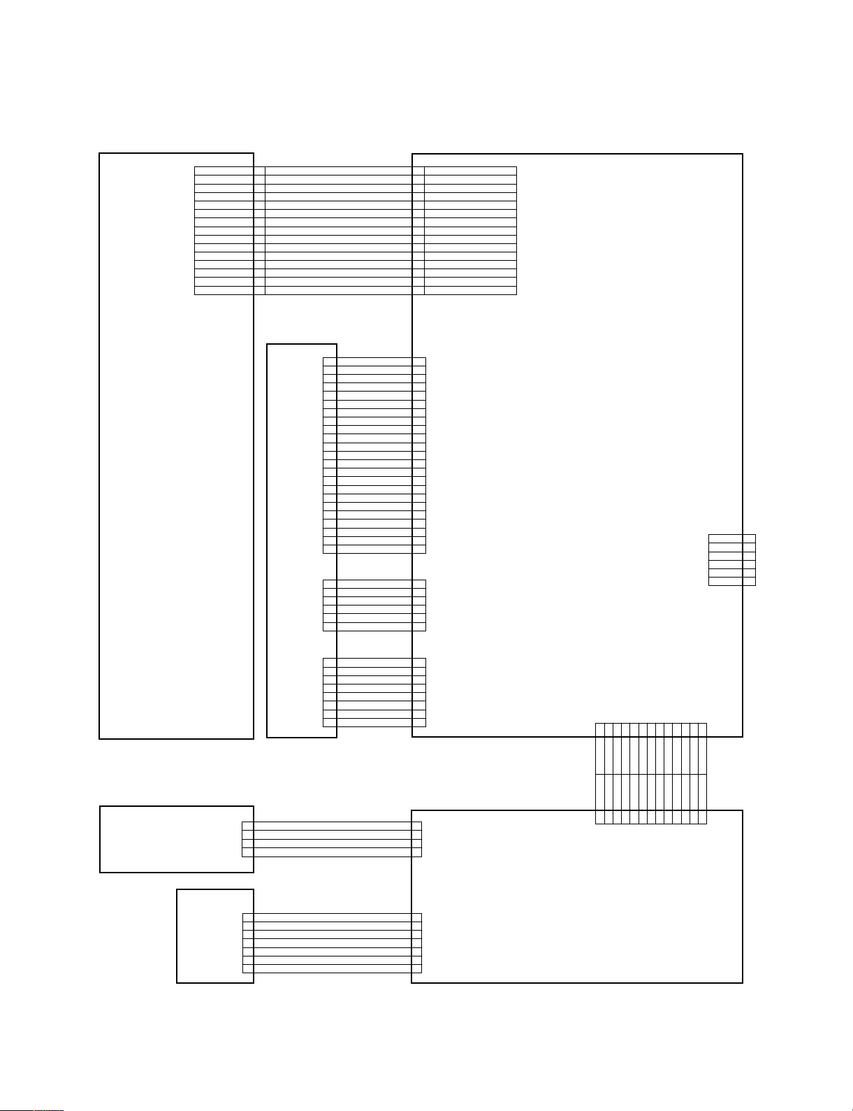
3. PRINTED WIRING BOARD AND SCHEMATIC DIAGRAM
16P(10P+6P)
CN801
Board-in
VCC+9.0V
GND
VCC-9.0V
PO SIG
E+5.0V
E+6.0V
VDD+5.0V
VDD+3V
GND
GND
M+8V
MGND
VKK-31V
F-(0.0)
F+(3.7V)
1
2
3
4
5
6
7
8
9
10
11
12
13
14
15
Press-fit
VCC+9.0V
1
2
3
4
5
6
7
8
9
10
11
12
13
14
15
GND
VCC-9.0V
PWON
E+5.0V
E+6.0V
VDD+5.0V
VDD+3V
GND
GND
M+8V
MGND
VKK-31V
FF+
CN701
EU02
POWER
EU04 POWER SW
CN105
1
2
3
4
Mechanism
FFC 1mm 23P
23
22
21
20
19
18
17
16
15
14
13
PUH
12
11
10
9
8
7
6
5
4
3
2
1
FFC 1.25mm 6P
6
5
4
TRAY
3
2
1
FFC 1mm 8P
8
7
6
5
MOTOR
4
3
2
1
W102
WIRE 2mm AWG26#2651
GND
E+5V
POWLED
POWKEY
W501
VCC
RF
LD2
MON2
VOR2
GND
VREF
VCC
F0
E0
A0
D0
C0
B0
F+
T-
T+
FVCC
GND
LD
MON
VOR
W502
GND
LDMP
TOPN
LDMN
TCLS
TRAY
W503
FMN
FMP
GND
LMT
DMN
DMP
VCC
DMFG
4P
1
2
3
4
5
6
7
8
9
10
11
CN501
12
13
14
15
16
17
18
19
20
21
22
23
1
2
3
CN502
4
5
6
1
2
3
4
CN503
5
6
7
8
1
2
CN102
3
4
EU01 MAIN
W602
FFC 1mm 13P
PWRCNT
RSTOX
PWRCNT
RSTOX
13
E+5V
E+5V
CN603
DSPRST
HMUTE
DSPRST
HMUTE
101112
CN101
DSPS0
DSPSI
DSPS0
DSPSI
987654321
DSPCKX
DSTBX
GND
DSPCKX
DSTBX
GND
CN601
VKK-31V
VKK-31V
1
GND
2
5V
3
TXD
4
CTS
5
RXD
6
RTS
13
121110
F+
F-
F+
F-
123456789
ENTER SW
EU03 FRONT
1
2
3
4
5
6
7
NC
LEFT
COMMON(GND)
DOWN
ENTER
RIGHT
UP
1
2
3
CN103
4
5
6
7
Fig. 3-3-1

4. BLOCK DIAGRAMS
4-1. Overall Block Diagram
Data/Control Bus
DVD AV Data
Tray
Motor
SPM
Motor Driver
IC503
BA5813FM-E2
IC606
MBM29F800BA-55PFTN
8M-FROM
IC601
S-24C04BFJ-TB
PUH
Feed
Motor
PUH Driver
&
EE-PROM
RF Amp.
IC502
TA1323F
IC605
TMP94C251AF
Main-CPU
M11B11664A-30T
IC402
IC401
TC94A03F
IC301
ZR36732
X601
9MHz
CeraOSC
1M-DRAM
Interated Data
processor
IC202
TC203G08AF-0103
AV-1Chip
Processor
MAIN PROCESSOR UNIT
27MHz
Xtal OSC
IC901
AD1958
Audio-DAC
IC912
NJM4580E
Audio LPF
Amplifire
IC304
MM1567AJBE
Video Driver
IEC958
Audio Out
Analog
Audio Out
YPBPR/S
Composite
SW POWER SUPPLY
1M-DRAM
IC603
M11B11664A-30T
16M-S-DRAM
IC305,306
HY57V161610DTC-8
Display
(FL)
Display-CPU
FRONT DISPLAY UNIT
IC101
TMP87CH74AF
Fig.3-4-1
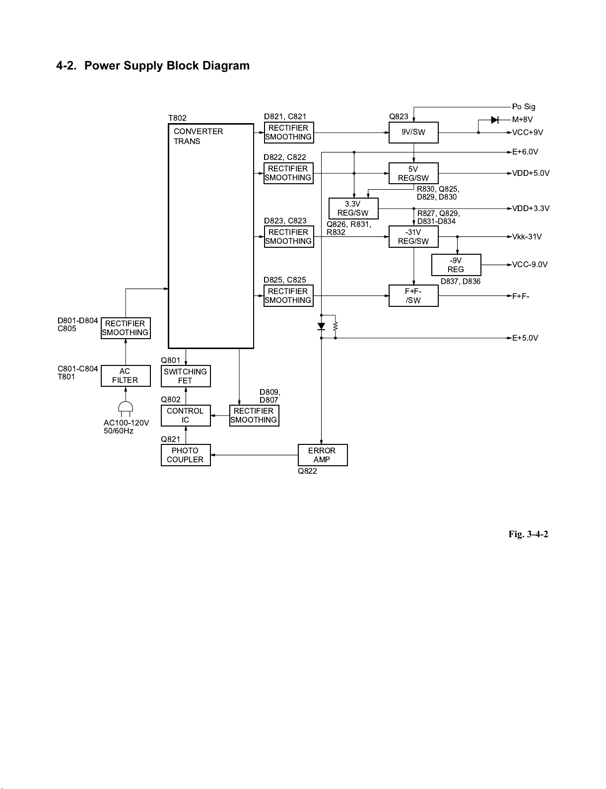
4-2. Power Supply Block Diagram
D801-D804
C805
C801-C804
T801
RECTIFIER
SMOOTHING
AC
FILTER
AC100-120V
50/60Hz
T802
CONVERTER
TRANS
Q801
SWITCHING
FET
Q802
CONTROL
IC
Q821
PHOTO
COUPLER
D821, C821
RECTIFIER
SMOOTHING
D822, C822
RECTIFIER
SMOOTHING
D823, C823
RECTIFIER
SMOOTHING
D825, C825
RECTIFIER
SMOOTHING
D809,
D807
RECTIFIER
SMOOTHING
ERROR
Q822
REG/SW
Q826, R831,
R832
AMP
3.3V
Q823
9V/SW
REG/SW
REG/SW
5V
R830, Q825,
D829, D830
R827, Q829,
D831-D834
-31V
F+F-
/SW
-9V
REG
D837, D836
Po Sig
M+8V
VCC+9V
E+6.0V
VDD+5.0V
VDD+3.3V
Vkk-31V
VCC-9.0V
F+F-
E+5.0V
Fig. 3-4-2
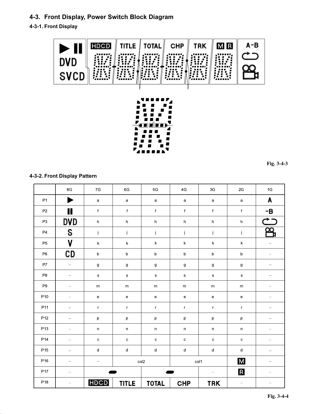
4-3. Front Display, Power Switch Block Diagram
4-3-1. Front Display
8G 7G 6G 5G 4G
4-3-2. Front Display Pattern
3G 2G 1G
a
h
r
(7G-2G)
j
k
s
n
p
d
f
g
e
col1col2
b
m
c
Fig. 3-4-3
P1
P2
P3
P4
P5
P6
P7
P8
P9
P10
P11
P12
P13
P14
8G 7G 6G
a
f
h
j
k
b
g
s
m
e
r
p
n
c
5G 4G 3G 2G 1G
a
f
h
j
k
b
g
s
m
e
r
p
n
c
a
f
h
j
k
b
g
s
m
e
r
p
n
c
a
f
h
j
k
b
g
s
m
e
r
p
n
c
a
f
h
j
k
b
g
s
m
e
r
p
n
c
a
f
h
j
k
b
g
s
m
e
r
p
n
c
P15
P16
P17
P18
d
d
col2 col1
d
d
d
d
Fig. 3-4-4
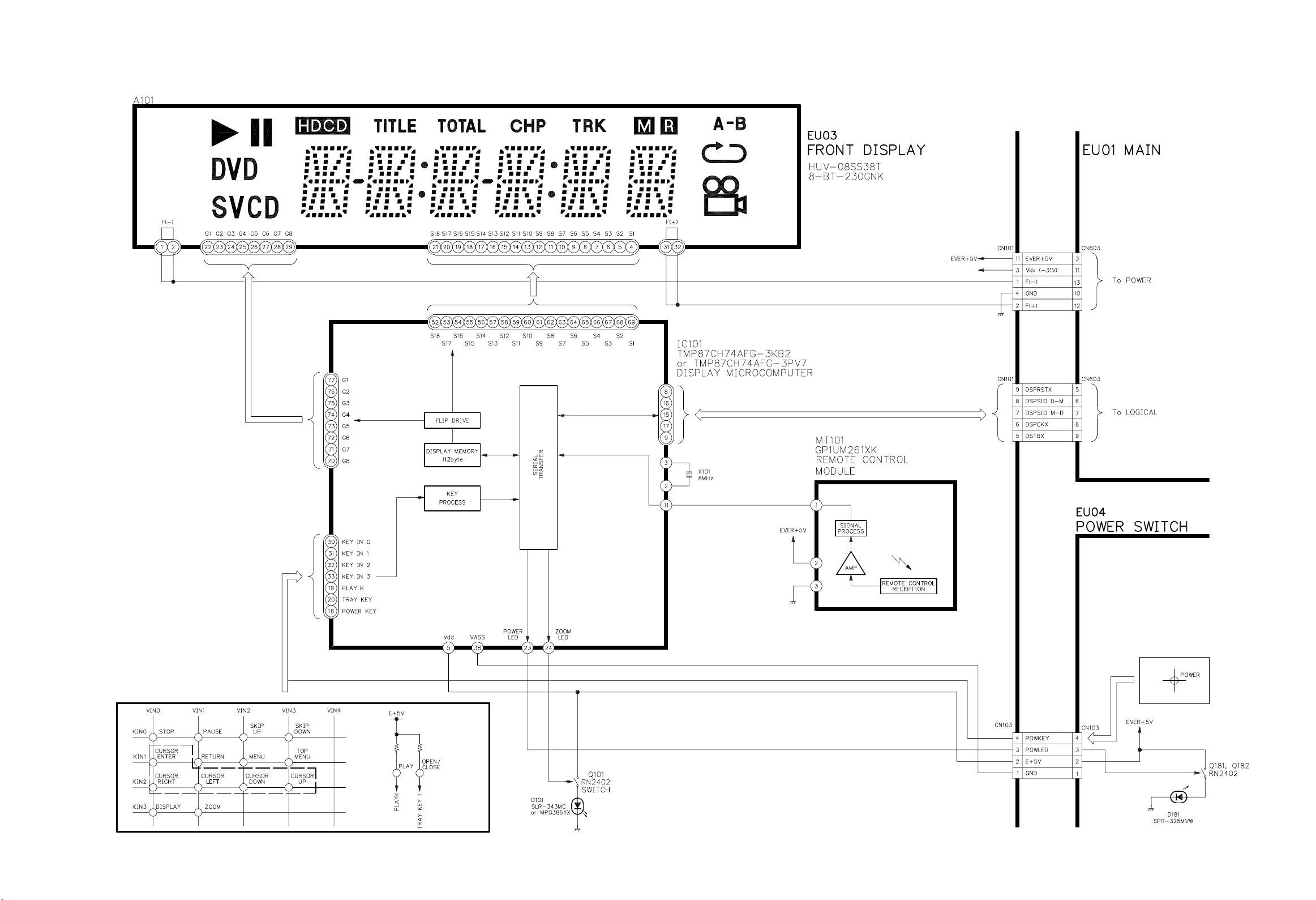
4-3-3. Front Display, Power Switch Block Diagram
Fig. 3-4-5
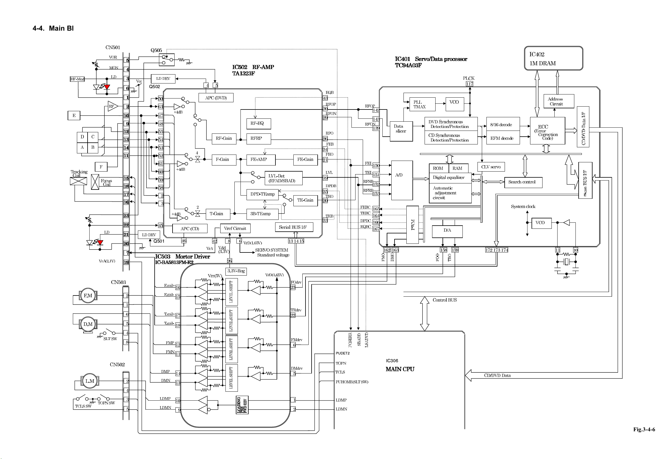
4-4. Main Block Diagrams
4-4-1. Servo System Block Diagram
Q502
m
Q501
PUDET2
IC306
Fig.3-4-6
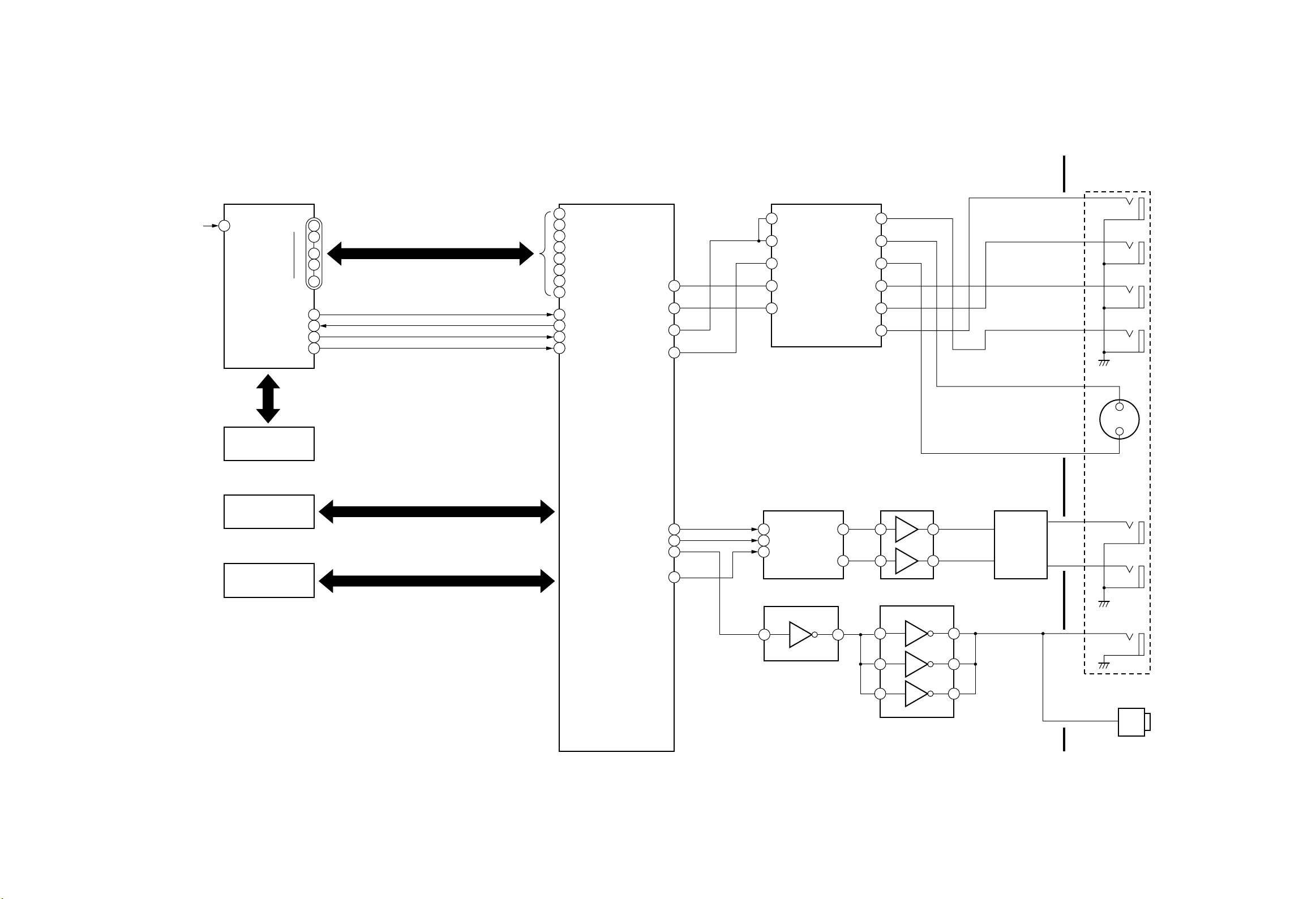
4-4-2. Logical System Block Diagram
From
IC502
PIN30
IC401
TC94A03F
DATA PRO-1
143
RFDVD
PDREQ
PDSYC
1M DRAM
IC402
M11B11664A-30T
16M FROM
IC309
MBM29LV160BE
64M-SDRAM
IC305
MT48LC2M32B2
PD0
PD7
PDCK
PD8
IC301
ZR36732
AV MAIN PROCESSOR
152
DVDDA0
60
62
65
67
69
73
72
71
70
DISC STREAM
DATA 8bit
153
DVDDA1
154
DVDDA2
155
DVDDA3
156
DVDDA4
157
DVDDA5
158
DVDDA6
159
DVDDA7
150
DVDSTRB
149
DVDALID
148
DVDSOS
147
DVDERR
CBOUT
C
R
OUT
COUT
YOUT
ABCLK
ALRCLK
SPDIF
AOUT 0
106
105
103
102
141
139
133
136
IC304
MM1567AJBE
VIDEO DRIVER
2
CIN
4
VIN
6
YIN1
14
B
IN
C
16
C
R
IN
IC901
AD1958
AUDIO DAC
5 23
BCK
4
LRCK
SD ATA
6
IC901
TC7SU04F
VOUTL
VOUTR
VOUT
COUT
YOUT1
YOUT2
C
R
C
20
B
OUT
OUT
27
25
23
20
18
16
IC912
NJM4580E
2 1
6 7
IC902
TC7WU04F
MAIN UNIT
Q910
HN-1C03F
MUTE
J301
C
Y
P
R
P
B
Y
COMPOSITE
VIDEO
S TERMINAL
Lch OUT
Rch OUT
2 4
1 7
3 5
6 2
IC914
TOTX178A
DIGITAL OUT
(COAXIAL)
Fig. 3-4-7
A
B
C
2 5 6 7 89
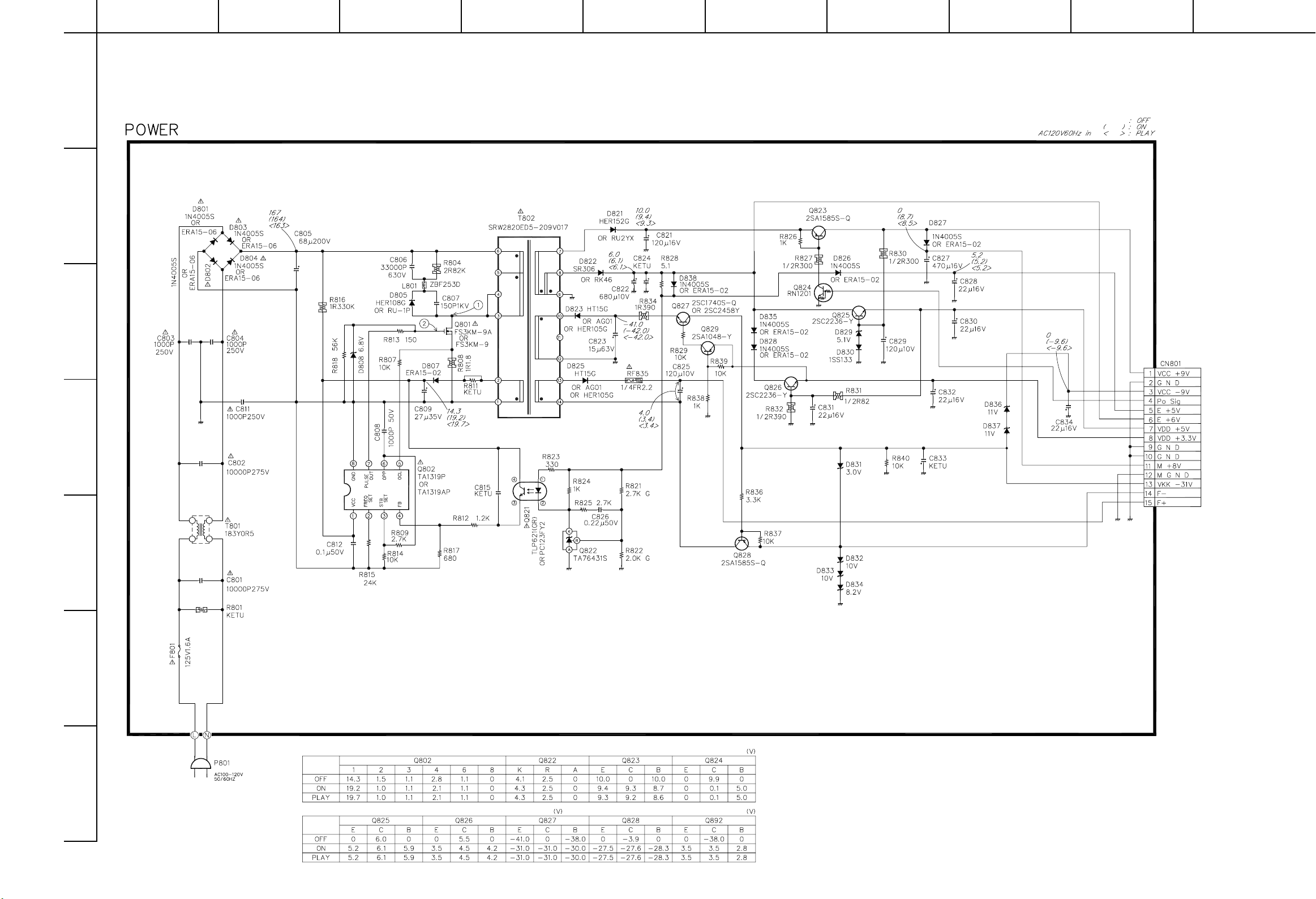
5. CIRCUIT DIAGRAMS
5-1. Power Supply Circuit Diagram
10134
D
E
F
G
Fig. 3-5-1
 Loading...