

Page 1

SERVICE MANUAL
DVD VIDEO PLAYER
SD-1300A
FILE NO. 810-200105
SD-1300H
SD-1300T
SD-1300Y
PRINTED IN JAPAN, Jun., 2001
S
Page 2
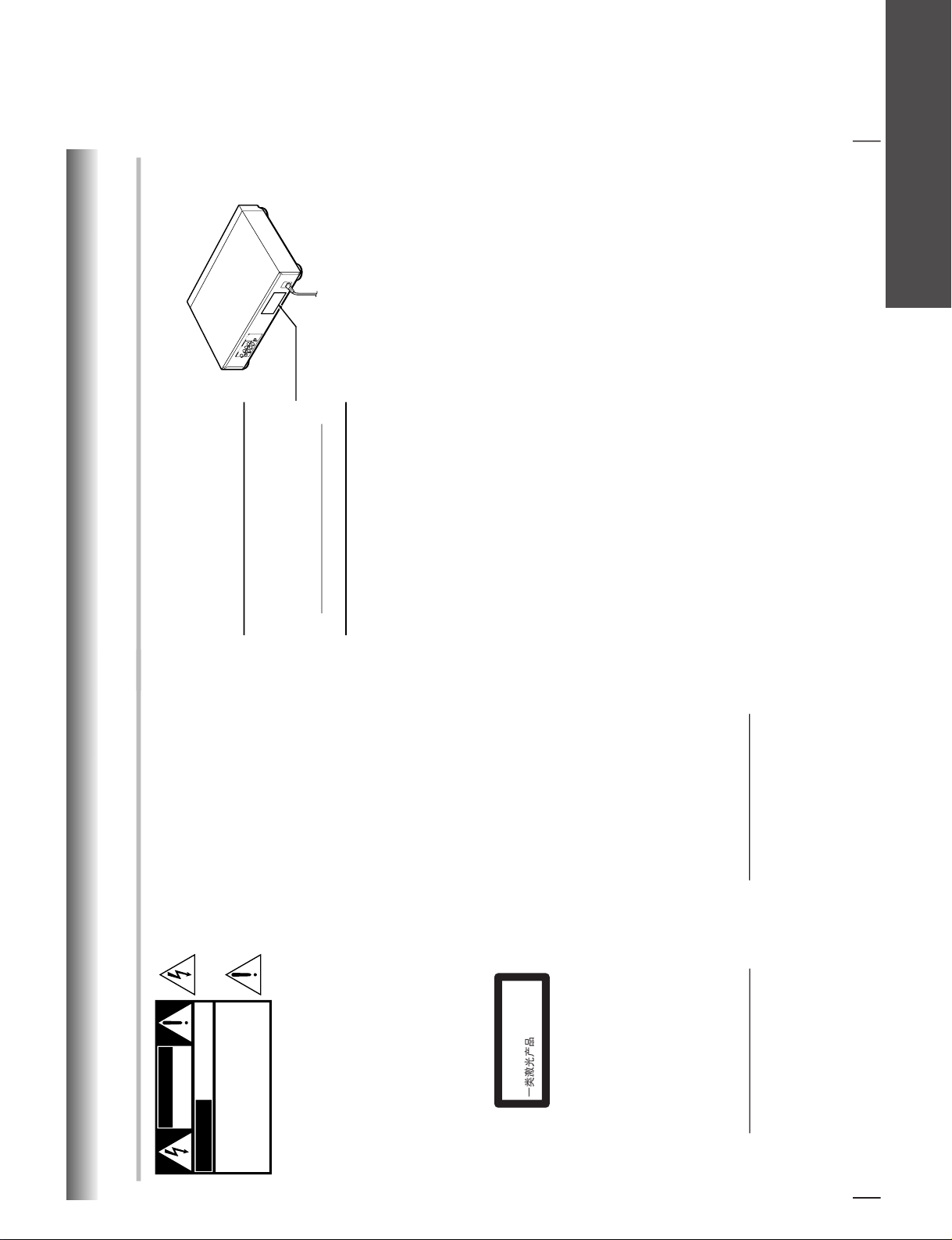
LASER BEAM CAUTION LABEL
When the power supply is being turned on, you may not remove this laser cautions label. If it removes, radiation of a laser
may be recceived.
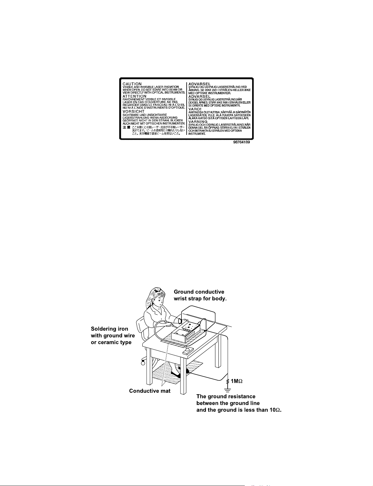
PREPARATION OF SERVICING
Pickup Head consists of a laser diode that is very susceptible to external static electricity.
Although it operates properly after replacement, if it was subject to electrostatic discharge during replacement,
its life might be shortened. When replacing, use a conductive mat, soldering iron with ground wire, etc. to
protect the laser diode from damage by static electricity.
And also, the LSI and IC are same as above.
Ground conductive
wrist strap for body.
Soldering iron
with ground wire
or ceramic type
1M
W
Conductive mat
The ground resistance
between the ground line
and the ground is less than 10W.
Page 3

CONTENTS
GENERAL DESCRIPTIONS
1. OPERATING INSTRUCTIONS................................................ 1- 1
2. LOCATION OF MAIN PARTS AND
MECHANISM PARTS ............................................................. 1-24
2-1. Location of Main Parts ..................................................... 1-24
2-2. Location of Mechanism Parts .......................................... 1-25
SECTION 1
3. TROUBLESHOOTING ............................................................ 1-29
3-1. Main Circuit....................................................................... 1-29
3-1-1. Servo System.................................................................. 1-29
3-1-2. Location Diagram of Servo Test Point........................ 1-36
PART REPLACEMENT AND ADJUSTMENT PROCEDURES
1. REPLACEMENT OF MECHANICAL PARTS ...................... 2-1
1-1. Cabinet Replacement .......................................................... 2-1
1-1-1. Top Cover ........................................................................ 2-1
1-1-2. Clamper Stay ................................................................... 2-1
1-1-3. Tray Panel ....................................................................... 2-2
1-1-4. Front Panel and Tray ..................................................... 2-3
1-1-5. Rear Panel........................................................................ 2-3
1-2. PC Board Replacement....................................................... 2-4
1-2-1. Main PC Board ............................................................... 2-4
1-2-2. Power PC board .............................................................. 2-4
1-2-3. Front PC Board............................................................... 2-5
SERVICING DIAGRAMS
1. STANDING PC BOARDS FOR SERVICING .........................3-1
2. CIRCUIT SYMBOLS AND
SUPPLEMENTARY EXPLANATION..................................... 3- 2
2-1. Precautions for Part Replacement..................................... 3-2
2-2. Solid Resistor Indication..................................................... 3-2
2-3. Capacitance Indication ....................................................... 3-2
2-4. Inductor Indication ............................................................. 3-3
2-5. Waveform and Voltage Measurement .............................. 3-3
2-6. Others ...................................................................................3-3
3. PRINTED WIRING BOARD AND
SCHEMATIC DIAGRAM.......................................................... 3-4
4. BLOCK DIAGRAMS.................................................................. 3-5
4-1. Overall Block Diagram ....................................................... 3-5
4-2. Power Supply Block Diagram ............................................ 3-7
4-3. Front Display, Power Switch Block Diagram................... 3-8
4-4. Main Block Diagrams ....................................................... 3-11
SECTION 2
1-3. Mechanism Parts ................................................................. 2-5
1-3-1. Mechanism Chassis Assembly........................................ 2-5
1-3-2. Loading Belt .................................................................... 2-6
1-3-3. Loading Motor ................................................................ 2-6
1-3-4. Sub Chassis (with a pickup mechanism) ....................... 2-7
1-3-5. Pickup Mechanism Assembly......................................... 2-7
1-3-6. Gear A Assembly, Gear B and
Rack Gear Assembly....................................................... 2-8
1-3-7. Feed Motor ...................................................................... 2-9
SECTION 3
5. CIRCUIT DIAGRAMS............................................................. 3-15
5-1. Power Supply Circuit Diagram........................................ 3-15
5-2. Front Display, Power Switch Circuit Diagram .............. 3-18
5-3. Main Circuit Diagram ...................................................... 3-21
5-4. Motor System Circuit Diagrams ...................................... 3-34
6. PC BOARDS .............................................................................. 3-35
6-1. Power Supply PC Board ................................................... 3-35
6-2. Power Switch PC Board ................................................... 3-36
6-3. Front Display PC Board ................................................... 3-37
6-4. Main PC Board.................................................................. 3-39
SAFETY PRECAUTION ................................................................. 4 -1
NOTICE ............................................................................................. 4-1
ABBREVIATIONS ........................................................................... 4-1
1. Integrated Circuit (IC) ............................................................ 4-1
2. Capacitor (Cap) ....................................................................... 4-1
3. Resistor (Res) ........................................................................... 4-1
SECTION 4
PARTS LIST
4. EXPLODED VIEWS................................................................... 4-2
4-1. Packing Assembly................................................................ 4-2
4-2. Chassis Assembly ................................................................ 4-3
4-3. Mechanism Assembly.......................................................... 4-4
5. PARTS LIST ................................................................................ 4-6
Page 4

This page is not printed.
Page 5
2
Introduction
WARNING: TO REDUCE THE RISK OF FIRE OR ELECTRIC SHOCK, DO NOT EXPOSE THIS APPLIANCE
TO RAIN OR MOISTURE. DANGEROUS HIGH VOLTAGES ARE PRESENT INSIDE THE
ENCLOSURE. DO NOT OPEN THE CABINET . REFER SERVICING TO QUALIFIED PERSONNEL
ONLY.
CAUTION: This Digital Video Disc Plzayer employs a Laser System.
To ensure proper use of this product, please read this owner’s manual carefully and retain for
future reference. Should the unit require maintenance, contact an authorized service location -
see service procedure.
Use of controls or adjustments or performance of procedures other than those specified herein
may result in hazardous radiation exposure.
To prevent direct exposure to laser beam, do not try to open the enclosure.
Visible and invisible laser radiation when open and interlocks defeated.
DO NOT STARE INTO BEAM.
In the spaces provided below, record the Model and Serial No. located on the rear panel of your DVD video
player.
Model No. Serial No.
Retain this information for future reference.
The lightning flash with arrowhead symbol, within an equilat-
eral triangle, is intended to alert the user to the presence of
uninsulated “dangerous voltage” within the product’s enclo-
sure that may be of sufficient magnitude to constitute a risk
of electric shock to persons.
The exclamation point within an equilateral triangle is in-
tended to alert the user to the presence of important operat-
ing and maintenance (servicing) instructions in the literature
accompanying the appliance.
WARNING
RISK OF ELECTRIC SHOCK
DO NOT OPEN
AVIS
RISQUE DE CHOC ELECTRIQUE NE
PAS OUVRIR
WARNING : TO REDUCE THE RISK OF
ELECTRIC SHOCK, DO NOT REMOVE
COVER (OR BACK). NO USERSERVICEABLE
PARTS INSIDE. REFER SERVICING TO
QUALIFIED SERVICE PERSONNEL.
SAFETY PRECAUTIONS
CLASS1 LASER PRODUCT
3
Introduction
Location of the required label
WARNING
TO REDUCE THE RISK OF
ELECTRIC SHOCK.
DO NOT REMOVE COVER.
REFER SERVICING TO QUALIFIED
SERVICE PERSONNEL.
TOS
H
IBA
CORPORATION
SECTION 1
GENERAL DESCRIPTIONS
GENERAL DESCRIPTIONS
1. OPERATING INSTRUCTIONS (SD-1300A/H)
SECTION 1
1-1
Page 6
4
Introduction
IMPORTANT SAFETY INSTRUCTIONS
CAUTION: PLEASE READ AND OBSERVE ALL WARNINGS AND INSTRUCTIONS GIVEN IN THIS
OWNER’S MANUAL AND THOSE MARKED ON THE UNIT. RETAIN THIS BOOKLET FOR
FUTURE REFERENCE.
This set has been designed and manufactured to assure personal safety. Improper use can result in electric
shock or fire hazard. The safeguards incorporated in this unit will protect you if you observe the following
procedures for installation, use and servicing. This unit is fully transistorized and does not contain any parts that
can be repaired by the user.
DO NOT REMOVE THE CABINET COVER, OR YOU MA Y BE EXPOSED TO DANGEROUS VOL T AGE.
REFER SERVICING TO QUALIFIED SERVICE PERSONNEL ONLY .
1. Read these instructions.
2. Keep these instructions.
3. Heed all warnings.
4. Follow all instructions.
5. Do not use this apparatus near water.
6. Clean only with dry cloth.
5
Introduction
7. Do not block any ventilation openings. Install in accordance with the
manufacturer’s instructions.
8. Do not install near any heat sources such as radiators, heat registers, stoves,
or other apparatus (including amplifiers) that produce heat.
9. Protect the power cord from being walked on or pinched particularly at plugs,
convenience receptacles, and the point where they exit from the apparatus.
10. Only use attachments/accessories specified by the manufacturer.
S3125A
11.Use only with the car t, stand, tripod, bracket, or table specified by the
manufacturer, or sold with the apparatus. When a cart is used, use caution
when moving the cart/apparatus combination to avoid injury from tip-over.
1-2
Page 7

6
Introduction
IMPORTANT SAFETY INSTRUCTIONS
12.Unplug this apparatus during lightning storms or when unused for long periods
of time.
13.Refer all servicing to qualified service personnel. Servicing is required when
the apparatus has been damaged in any way, such as power-supply cord or
plug is damaged, liquid has been spilled or objects have fallen into the
apparatus, the apparatus has been exposed to rain or moisture, does not
operate normally, or has been dropped.
14.When you use headphones, keep the volume at a moderate level. If you use
the headphones continuously with high volume sound, it may cause hearing
damage.
15.Do not overload wall outlets; extension cords, or integral convenience
receptacles as this can result in a risk of fire or electric shock.
16.Nev er insert objects of any kind into this apparatus through openings as they
may touch dangerous voltage points or short-out parts that could result in a
fire or electric shock. Never spill liquid of any kind on the apparatus.
7
Introduction
17. Keep your fingers well clear of the disc tray as it is closing. Neglecting to do
so may cause serious personal injury.
18.Do not place a heavy object on or step on the apparatus. The object may f all,
causing serious personal injury and serious damage to the apparatus.
19. Do not use a cracked, deformed, or repaired disc. These discs are easily
broken and may cause serious personal injury and apparatus malfunction.
1-3
Page 8
8
Introduction
Precautions
Notes on handling
When shipping the DVD video player, the original
shipping carton and packing materials come in handy.
For maximum protection, repack the unit as it was
originally packed at the factory.
Do not use volatile liquids, such as insect spray, near
the DVD video player. Do not leave rubber or plastic
products in contact with the DVD video player for a
long time. They will leave marks on the finish.
The top and rear panels of the DVD video player may
become warm after a long period of use. This is not a
malfunction.
When the DVD video player is not in use, be sure to
remove the disc and turn off the power.
If you do not use the DVD video player for a long
period, the unit may not function properly in the
future. Turn on and use the DVD video player
occasionally.
Notes on locating
Place the DVD video player on a level surface. Do not
use it on a shaky or unstable surface such as a
wobbling table or inclined stand. The loaded disc may
come off the proper position and cause damage to
the DVD video player.
When you place this DVD video player near a TV,
radio, or VTR, the playback picture may become poor
and the sound may be distorted. In this case, place
the DVD video player away from the TV, radio, or
VTR.
Notes on cleaning
Use a soft, dry cloth for cleaning.
For stubborn dirt, soak the cloth in a weak detergent
solution, wring well and wipe. Use a dry cloth to wipe
it dry.
Do not use any type of solvent, such as thinner and
benzine, as they may damage the surface of the DVD
video player.
If you use a chemical saturated cloth to clean the unit,
follow that product’s instructions.
To obtain a clear picture
The DVD video player is a high technology, precision
device. If the optical pick-up lens and disc drive parts
are dirty or worn down, the picture quality becomes
poor. To obtain a clear picture, we recommend regular
inspection and maintenance (cleaning or parts
replacement) every 1,000 hours of use depending on
the operating environment. For details, contact your
nearest dealer.
Notes on moisture condensation
Moisture condensation damages the DVD video
player. Please read the following carefully.
Moisture condensation occurs, for example, when you
pour a cold drink into a glass on a warm day. Drops of
water form on the outside of the glass. In the same way,
moisture may condense on the optical pick-up lens
inside this unit, one of the most crucial internal parts of
the DVD video player.
Moisture condensation occurs during the
following cases.
When you bring the DVD video player directly from a
cold place to a warm place.
When you use the DVD video player in a room where
you just turned on the heater, or a place where the
cold wind from the air conditioner directly hits the unit.
In summer, when you use the DVD video player in a
hot and humid place just after you move the unit from
an air conditioned room.
When you use the DVD video player in a humid place.
Do not use the DVD video player when moisture
condensation may occur.
If you use the DVD video player in such a situation, it
may damage discs and internal parts. Remove the
disc, connect the power cord of the DVD video player
to the wall outlet, turn on the DVD video player, and
leave it for two or three hours. After two or three
hours, the DVD video player will have warmed up and
evaporated any moisture. Keep the DVD video player
connected to the wall outlet and moisture
condensation will seldom occur.
E
x
a
m
p
l
e
o
f
m
o
i
s
t
u
r
e
c
o
n
d
e
n
s
a
t
i
o
n
!
Optical pick-up
lens
It’s too
warm!
Wait!
Wall outlet
9
Introduction
Notes on Discs
On handling discs
Do not touch the playback side of the disc.
Do not attach paper or tape to discs.
On cleaning discs
Fingerprints and dust on the disc cause picture and
sound deterioration. Wipe the disc from the center
outwards with a soft cloth. Always keep the disc
clean.
If you cannot wipe off the dust with a soft cloth, wipe
the disc lightly with a slightly moistened soft cloth and
finish with a dry cloth.
Do not use any type of solvent such as thinner,
benzine, commercially available cleaners or antistatic
spray for vinyl LPs. It may damage the disc.
On storing discs
Do not store discs in a place subject to direct sunlight
or near heat sources.
Do not store discs in places subject to moisture and
dust such as a bathroom or near a humidifier.
Store discs vertically in a case. Stacking or placing
objects on discs outside of their case may cause
warping.
Playback side
DVD video disc
Title 1
Title 2
Chapter 1 Chapter 2 Chapter 1 Chapter 2 Chapter 3
Track 1 Track 2 Track 3 Track 4 Track 5
Structure of disc contents
Normally, DVD video discs are divided into titles, and
the titles are sub-divided into chapters. VIDEO CDs/
audio CDs are divided into tracks.
DVD video disc
VIDEO CD/audio CD
Each title, chapter or track is assigned a number, which
is called “title number”, “chapter number” or “track
number” respectively.
There may be discs that do not have these numbers.
Notes on copyright
It is forbidden by law to copy, broadcast, show,
broadcast on cable, play in public, and rent copyrighted
material without permission.
DVD video discs are copy protected, and any recordings
made from these discs will be distorted.
This product incorporates copyright protection
technology that is protected by method claims of certain
U.S. patents and other intellectual property rights owned
by Macrovision Corporation and other rights owners.
Use of this copyright protection technology must be
authorized by Macrovision Corporation, and is intended
for home and other limited viewing uses only unless
otherwise authorized by Macrovision Corporation.
Reverse engineering or disassembly is prohibited.
VIDEO CD/audio CD
1-4
Page 9
10
Introduction
DIGITAL VIDEO
About this owner’s manual
This owner’s manual explains the basic instructions of
this DVD video player. Some DVD video discs are
produced in a manner that allows specific or limited
operation during playback. As such, the DVD video
player may not respond to all operating commands. This
is not a defect in the DVD video player. Refer to
instruction notes of discs.
“
” may appear on the TV screen during operation.
A “
” means that the operation is not permitted by the
DVD video player or the disc.
Notes on region numbers
The DVD video player is allotted one of region numbers,
which stand for their playable area. If the numbers are
printed on your DVD video disc, and are different from
that of the DVD video player, disc playback will not be
allowed by the player. (In this case, the DVD video player
displays the message.)
The region number of this DVD video player is printed
on the rear panel of the main unit and on the carton.
On VIDEO CDs
This DVD video player supports VIDEO CDs equipped
with the PBC (Version 2.0) function. (PBC is the
abbreviation of Playback Control.) You can enjoy two
playback variations depending on types of discs.
• VIDEO CD not equipped with PBC function
(Version 1.1)
Sound and movie can be played on this DVD video
player in the same way as an audio CD.
• VIDEO CD equipped with PBC function
(Version 2.0)
In addition to operation of a VIDEO CD not equipped
with the PBC function, you can enjoy playback of
interactive software with search function by using the
menu displayed on the TV screen (Menu Playback).
Some of the functions described in this owner’s
manual may not work with some discs.
Playable discs
This DVD video player can play the following discs.
• You cannot play discs other than those listed above.
• You cannot play discs of DVD-RAM, DVD-RW, etc.,
even if they may be labeled marks listed above.
• This DVD video player uses the NTSC/PAL color
system, and cannot play DVD video discs recorded in
any other color system (SECAM, etc.).
Notes on Discs (continued)
DVD
video
discs
Disc Mark
Contents
Disc
Size
Maximum
playback time
VIDEO
CDs
Approx. 4 hours
(single sided disc)
Approx. 8 hours
(double sided disc)
Approx. 80 minutes
(single sided disc)
Approx. 160 minutes
(double sided disc)
Approx. 74 minutes
Approx. 20 minutes
8 cm
12 cm
8 cm
12 cm
Audio
+
video
(moving
pictures)
Audio
+
video
(moving
pictures)
Audio
CDs
Approx. 74 minutes
Approx. 20 minutes
8 cm
(CD
single)
12 cm
Audio
The following discs are also available.
CD-R
CD-RW
CD-R/RW discs recorded by CD-DA method can be
played. Some CD-R/RW discs may be incompatible.
11
Introduction
Table of Contents
Introduction
SAFETY PRECAUTIONS .......................... 2
IMPORTANT SAFETY INSTRUCTIONS ...4
Precautions ............................................... 8
Notes on Discs..........................................9
Notes on region numbers ............................... 10
Table of Contents....................................11
Identification of Controls .......................12
Front panel ..................................................... 12
Rear panel...................................................... 12
DVD display....................................................13
Remote control ............................................... 14
Loading batteries............................................ 15
Operating with the remote control .................. 15
Connections
Connecting to a TV .................................16
Connecting to a TV.........................................16
Connecting to an audio system and TV
equipped with component video inputs ........ 17
Connecting to Optional Equipment ......18
Connecting to an amplifier equipped with a
Dolby Digital decoder ................................... 18
Connecting to an amplifier equipped with
Dolby Pro Logic Surround ............................ 18
Connecting to an amplifier equipped with a
DTS decoder ................................................ 18
Connecting to an amplifier equipped with an
MPEG2 audio decoder................................. 19
Connecting to an amplifier equipped with a
digital audio input ......................................... 19
Basic playback
Playing a Disc .........................................20
Basic playback ............................................... 20
Playing in fast reverse or fast forward
directions...................................................... 22
Playing frame by frame................................... 22
Playing in slow-motion....................................23
Resuming playback from the same location...23
Locating a Specific Title, Chapter, or
Track ........................................................24
Locating a title using the top menu.................24
Locating a title by entering the title number....24
Locating a specific chapter or track directly ... 25
Locating a specific chapter or track................ 25
Advanced playback
Accessing a Specific Location Directly ...
26
Entering the time of the desired location ........ 26
Playing Repeatedly.................................27
Repeating a title, chapter, or track.................. 27
Repeating a specific segment ........................ 27
Playing in a Favorite Order ....................28
Setting titles, chapters, or tracks in a favorite
order............................................................. 28
Playing in Random Order.......................29
Playing titles, chapters or tracks in random
order............................................................. 29
Zooming a Picture ..................................30
Zooming a picture...........................................30
Selecting the Picture Enhancement
(E.P.M.) .....................................................31
Selecting the picture enhancement ................ 31
Selecting the Sound Enhancement
(E.A.M.) ....................................................32
Selecting the sound enhancement ................. 32
Selecting the Camera Angle .................. 33
Changing the camera angle ........................... 33
Selecting Subtitles .................................34
Selecting a subtitle language ......................... 34
Selecting a Language.............................35
Selecting a playback audio setting ................. 35
Operating in the On-screen Display Mode....
36
Operating in the on-screen display mode.......36
Function setup
Customizing the Function Settings ......38
Setting procedure ........................................... 38
Setting details................................................. 40
Others
Table of Languages................................46
Before Calling Service Personnel ......... 47
Specifications .........................................48
1-5
Page 10
12
Introduction
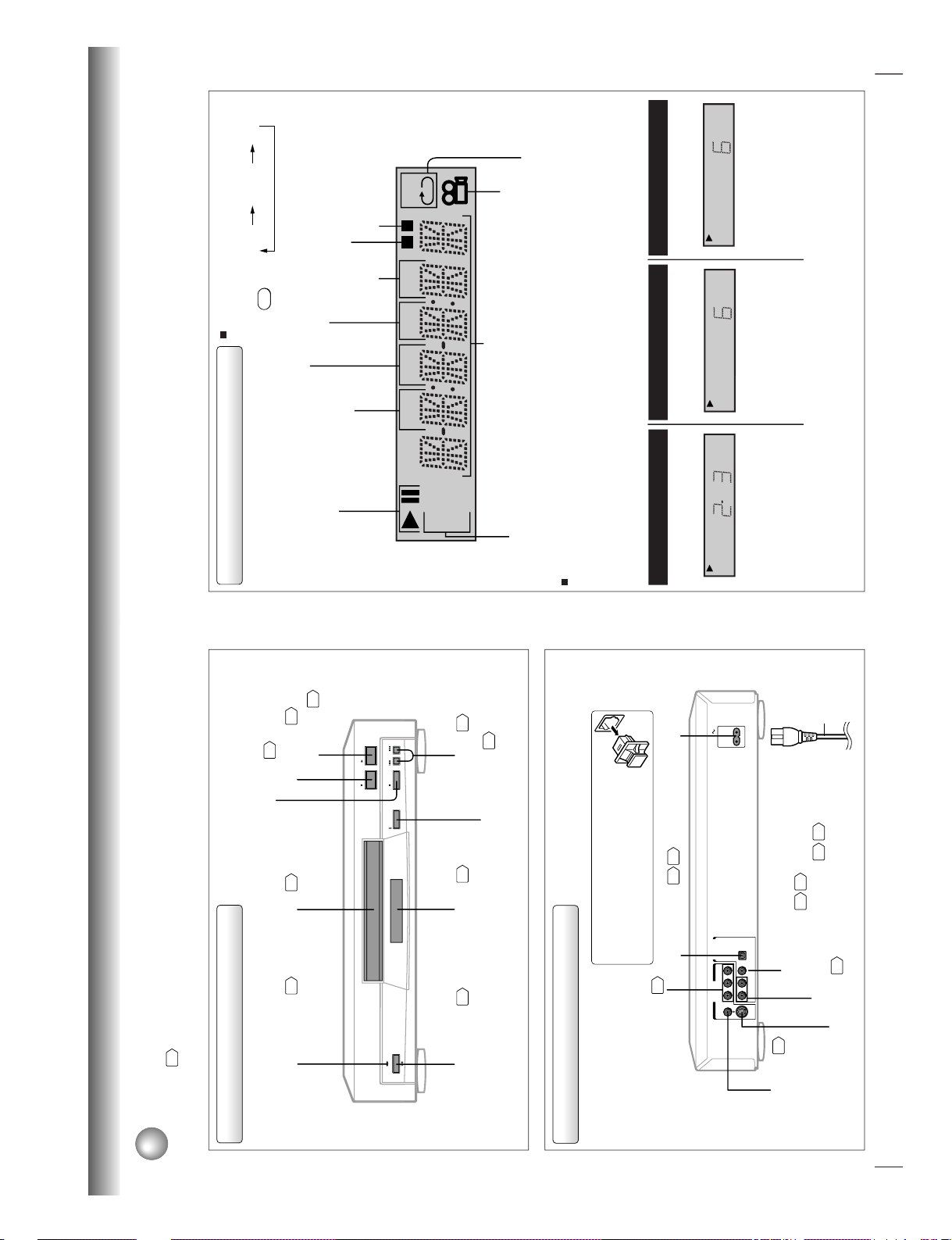
Identification of Controls
See the page in
for details.
Front panel
Rear panel
PAUSE
SKIP
OPEN/CLOSE
ON/STANDBY
PLAYSTOP
ON/STANDBY button
20
DVD display
13
OPEN/CLOSE button
20
SKIP buttons
25
STOP button
21
PLAY button
20
PAUSE button
21
ON/STANDBY indicator
20
Disc tray
20
BITSTREAM/PCM
AC IN
L
COAXIAL OPTICAL
ANALOG
R
VIDEO Y P
B PR
S
AUDIO OUT
VIDEO OUT
AC inlet
Power cord
VIDEO OUT (Y/P
B
/P
R
)
(Component video) jacks
ANALOG AUDIO OUT (L/R) jacks
16
18
19
18 19
16
S VIDEO OUT jack
VIDEO OUT jack
17
BITSTREAM/PCM COAXIAL
AUDIO OUT jack
BITSTREAM/PCM OPTICAL
AUDIO OUT jack
16 17
When connecting the optical digital cable, remove
the cap and fit the connector into the jack firmly.
When not using the jack, keep the cap inserted
to protect it from dust intrusion.
13
Introduction
DVD
VCD
TITLE TOTAL
CHP TRK
M A
-
BR
DVD display
Pressing of the FL DIM button on the remote
control changes the brightness of the display.
Repeat playback indicator
Angle icon indicator
Total playing time indicator
Memory playback indicator
Chapter number indicator
Title number indicator
Play mode indicator
Multifunctional indicator (indicates operating status or
messages, etc.)
Normal
Off
FL DIM
Dimmed
The indicators vary depending on the kinds of discs you play.
DVD video disc
Audio CD
Some discs may not display chapter
numbers or elapsed time.
• During playback:
Playing chapter 3 of title 2
Example
• During playback:
Example
Playing track 6
VIDEO CD
• During playback:
Example
Playing track 6
Some discs may not display track
numbers or elapsed time.
DVD
TITLE
CHP
VCD
TRK
CD
TRK
Track number
indicator
Random playback indicator
When you start playback, the elapsed time indicators appear. Pressing the FL SELECT button switches
them to the title/chapter/track number indicators. Some discs may not permit this operation.
DVD/VIDEO CD/CD indicator
1-6
Page 11
14
Introduction
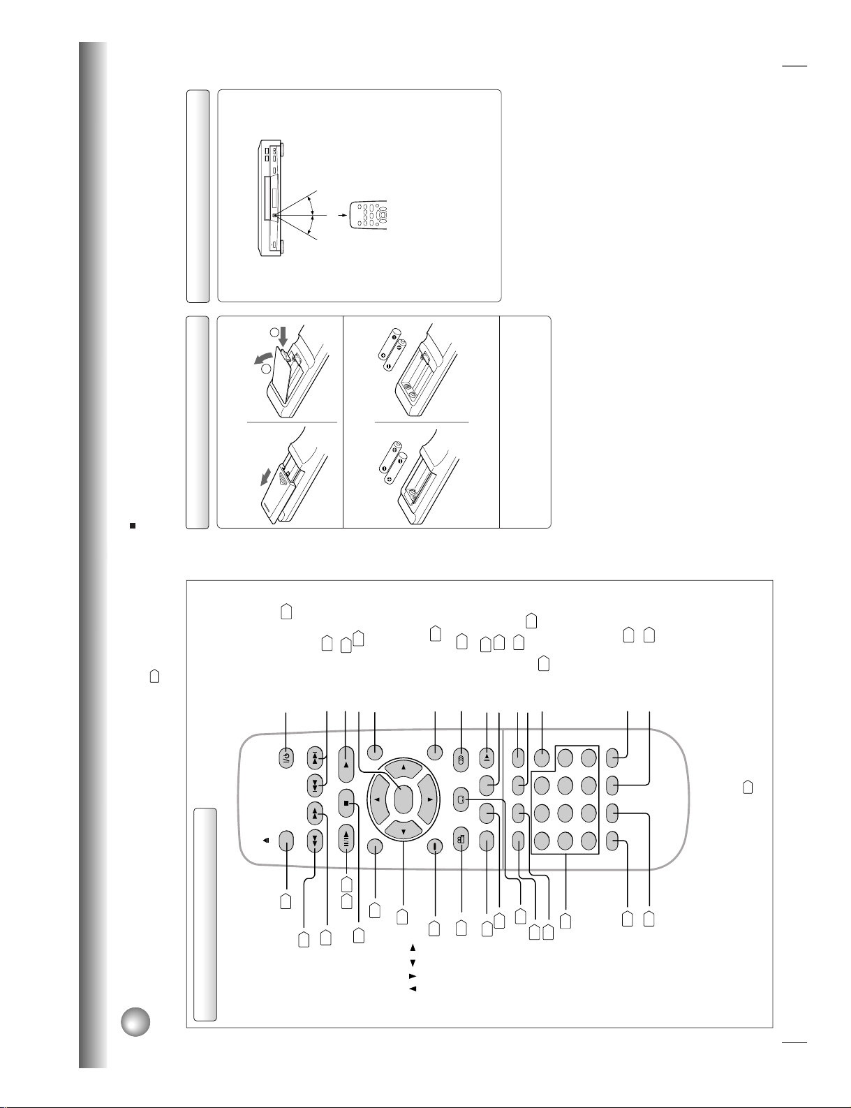
Identification of Controls (continued)
The instructions in this manual describe the functions on the remote control. See the page in
for details.
Remote control
* MENU button
Use the MENU button to display the menu included on
many DVD video discs. To operate a menu, follow the
instructions in “Locating a title using the top menu.”
24
TOP MENU
MENU
ENTER
RETURN
CLEAR
21
456
78
3
90
+10
T
RANDOM
REPEAT
A-B RPT
ANGLE SUBTITLE AUDIO
SETUP SLOWZOOMDISPLAY
MEMORY
SEARCH
SKIPREV
STOP PLAY
PAUSE/STEP
FWD
OPEN/CLOSE
FL SELECT
E.A.M. E.P.M.
FL DIM
OPEN/CLOSE button20PAUSE/STEP button
21 22
SETUP button
38
ANGLE button
33
34
SUBTITLE button
TOP MENU button
24
CLEAR button
25
REV button22FWD button
22
21
E.A.M. button
32
E.P.M. button
31
STOP button
RANDOM button
29
MEMORY button
28
MENU button*
RETURN button
38
ENTER button
38
FL DIM button
PLAY button
20
SKIP buttons
25
A-B RPT button
REPEAT button
ON/STANDBY button
20
SLOW button
23
ZOOM button
30
AUDIO button
35
Direction buttons
( / / / )
38
Number buttons
24
DISPLAY button
36
T button
24
27
27
13
FL SELECT button
13
15
Introduction
Operating with the remote control
Point the remote control at the remote
sensor and press the buttons.
Distance: About 7 m from the front of the remote
sensor
Angle: About 30° in each direction of the front of
the remote sensor
* Do not expose the remote sensor of the DVD video
player to a strong light source such as direct
sunlight or other illumination. If you do so, you may
not be able to operate the DVD video player via the
remote control.
Notes on the remote control
• Direct the remote control at the remote sensor of the DVD
video player.
• Do not drop or give the remote control a shock.
• Do not leave the remote control near an extremely hot or
humid place.
• Do not spill water or put anything wet on the remote
control.
• Do not open the remote control.
Within about 7 m
30°
30°
Open the cover.
Insert batteries (R6 size).
Make sure to match the + and – on the batteries
to the marks inside the battery compartment.
Close the cover.
Notes on batteries
Improper use of batteries may cause battery leakage and
corrosion. To operate the remote control correctly, follow the
instructions below.
• Do not insert batteries into the remote control in the wrong
direction.
• Do not charge, heat, open, or short-circuit the batteries.
Do not throw batteries into a fire.
• Do not leave dead or exhausted batteries in the remote
control.
• Do not use different types of batteries together, or mix old
and new batteries.
• If you do not use the remote control for a long period of
time, remove the batteries to avoid possible damage from
battery corrosion.
• If the remote control does not function correctly or if the
operating range becomes reduced, replace all batteries
with new ones.
• If battery leakage occurs, wipe the battery liquid from the
battery compartment, then insert new batteries.
1
2
3
Loading batteries
1
2
About the illustrations of the battery compartment
There are two types of battery compartment in the
supplied remote controls. (This does not mean a
difference in performance between the two.)
Refer to either illustration depending on the actual
remote control.
1-7
Page 12
16
Connections
BITSTREAM/PCM
AC IN
L
COAXIAL OPTICAL
ANALOG
R
VIDEO Y P
B
P
R
S
AUDIO OUT
VIDEO OUT
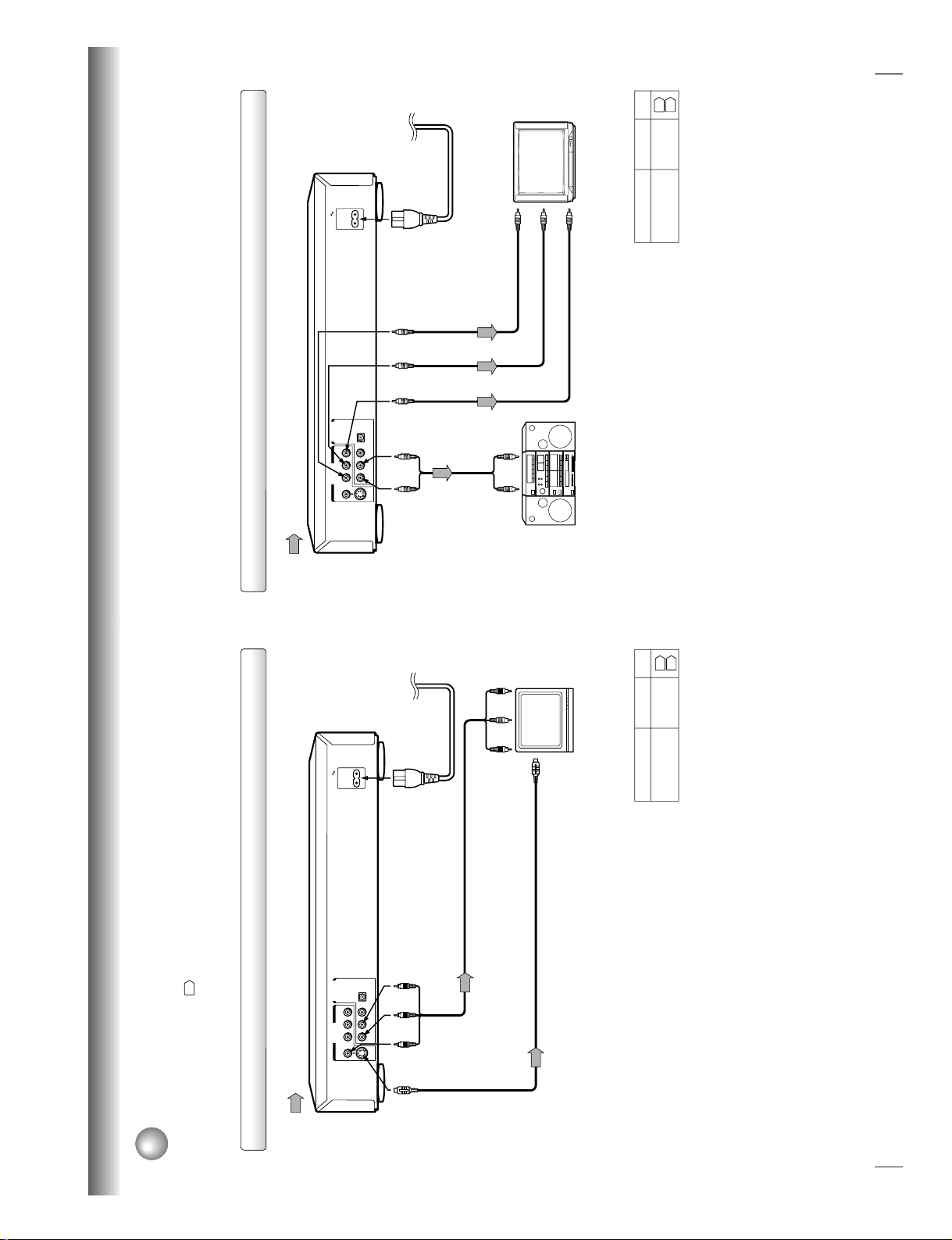
Connecting to a TV
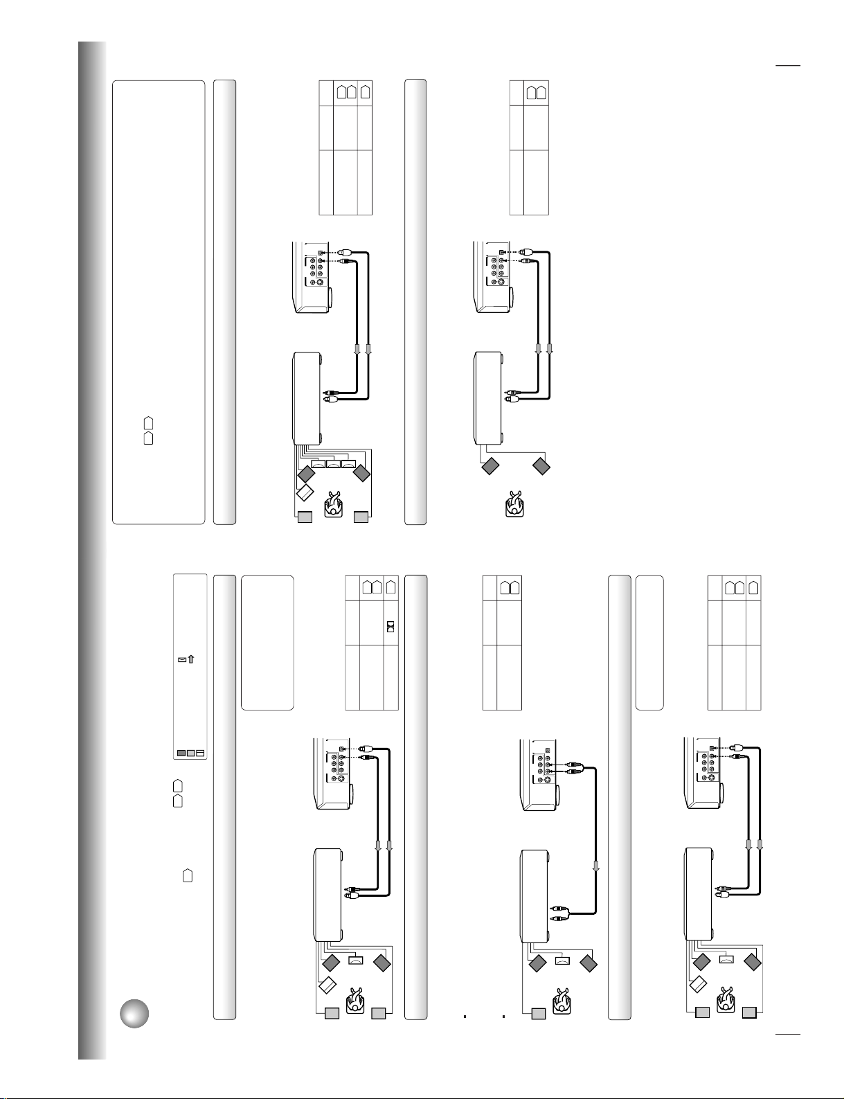
Connect the DVD video player to your TV.
For details of output sound, see
35
.
Connecting to a TV
T o VIDEO
OUT
To ANALOG AUDIO OUT
(red) (white)
(yellow)
Signal flow
To wall outlet
To video input
(yellow)
(red)
(white)
To S video input
Audio/video cable (supplied)
S video cable (not supplied)
To audio inputs
If the TV has an S video input, connect the
DVD video player with an S video cable.
When using an S video cable, do not
connect the yellow video cable.
Notes
• Refer to the owner’s manual of the connected TV as well.
• When you connect the DVD video player to your TV, be sure to turn off the power and unplug both units from the wall outlet
before making any connections.
• If your television set has one audio input, connect the DVD video player to a Y cable adapter (not supplied) and then connect
to your TV.
• Connect the DVD video player directly to your TV. If you connect the DVD video player to a VTR, TV/VTR combination or
video selector, the playback picture may be distorted as DVD video discs are copy protected.
• Make the following setting.
On-screen display
Select:
Page
“Analog 2ch”
“Audio Out Select”
TV or monitor with
audio/video inputs
38
40
To S VIDEO
OUT
17
Connections
BITSTREAM/PCM
AC IN
L
COAXIAL OPTICAL
ANALOG
R
VIDEO Y P
B
P
R
S
AUDIO OUT
VIDEO OUT
To PRVIDEO
OUT
Notes
• Refer to the owner’s manual of the connected equipment as well.
• When you connect the DVD video player to other equipment, be sure to turn off the power and unplug all of the equipment
from the wall outlet before making any connections.
• If you place the DVD video player near a tuner or radio, the radio broadcast sound might be distorted. In this case, place the
DVD video player away from the tuner and radio.
• The output sound of the DVD video player has a wide dynamic range. Be sure to adjust the receiver’s volume to a moderate
listening level. Otherwise, the speakers may be damaged by a sudden high volume sound.
• Turn off the amplifier before you connect or disconnect the DVD video player’s power cord. If you leave the amplifier power
on, the speakers may be damaged.
Connecting to an audio system and TV equipped with component video inputs
Signal flow
To wall outlet
To audio inputs of
the amplifier
(red)
(white)
(red) (white)
To Y
VIDEO
OUT
To P
B
VIDEO
OUT
To Y video input
To P
B
video input
To P
R
video input
TV or monitor with
component video inputs
Audio system
Component video outputs/inputs
Some TVs or monitors are equipped with component video inputs. Connecting to
these inputs allows you to enjoy higher quality picture playback.
Actual labels for component video inputs may vary depending on the TV
manufacturer. (ex. “Y, R-Y, B-Y” or “Y, C
B
, C
R
”)
In some TVs or monitors, the color levels of the playback picture may be reduced
slightly or the tint may change. In such a case, adjust the TV or monitor for
optimum performance.
• Make the following setting.
On-screen display
Select:
Page
“Analog 2ch”
“Audio Out Select”
To ANALOG AUDIO OUT
38
40
1-8
Page 13
18
Connections
BITSTREAM/PCM
L
COAXIAL OPTICAL
ANALOG
R
VIDEO Y P
B
P
R
S
AUDIO OUT
VIDEO OUT
BITSTREAM/PCM
L
COAXIAL OPTICAL
ANALOG
R
VIDEO Y P
B
P
R
S
AUDIO OUT
VIDEO OUT
BITSTREAM/PCM
L
COAXIAL OPTICAL
ANALOG
R
VIDEO Y P
B PR
S
AUDIO OUT
VIDEO OUT
Connecting to Optional Equipment
You can enjoy high quality dynamic sounds by connecting the DVD video player
to optional audio equipment.
For connection to your TV, see “Connecting to a TV”
16
17
.
For details of output sound, see
35
.
: Front speaker
: Rear speaker
: Sub woofer
: Center speaker
: Signal flow
Connecting to an amplifier equipped with a Dolby Digital decoder
Connecting to an amplifier equipped with Dolby Pro Logic Surround
Dolby Pro Logic Surround
You can enjoy the dynamic realistic sound of Dolby Pro Logic Surround by connecting an amplifier and speaker system (right and left
front speakers, a center speaker, and one or two rear speakers).
Connecting to an amplifier equipped with a DTS decoder
Digital Theater Systems (DTS)
DTS is a high quality surround technology used in theaters and now available for home use,
on DVD video discs or audio CDs.
If you have a DTS decoder or processor, you can obtain the full benefit of 5.1 channel DTS
encoded sound tracks on DVD video discs or audio CDs.
Manufactured under license from Dolby
Laboratories. “Dolby”, “Pro Logic”, and
the double-D symbol are trademarks of
Dolby Laboratories. Confidential
unpublished works. ©1992-1997 Dolby
Laboratories. All rights reserved.
• Use DVD video discs encoded via
the Dolby Digital recording
system.
• Make the following setting.
• Use DVD video discs or audio
CDs encoded via the DTS
recording system.
• Make the following setting.
Be sure to set “Audio Out Select”
to “Analog 2ch” when you enjoy
sounds of Dolby Pro Logic
Surround using this connection.
* Connect one or two rear speakers.
The output sound from the rear speakers will be
monaural even if you connect two rear speakers.
• Make the following setting.
“DTS” and “DTS Digital Surround” are
trademarks of Digital Theater Systems,
Inc.
On-screen display Select:
Page
“Bitstream”“Audio Out Select”
Recording system
On-screen display
Select:
Page
“Bitstream”
“Audio Out Select”
Recording system DTS
On-screen display
Select:
Page
“Analog 2ch”
“Audio Out Select”
With an amplifier equipped with Dolby Digital
Connect the equipment the same way as described in “Connecting to an amplifier
equipped with a Dolby Digital decoder.” Refer to that amplifier’s owner’s manual and set
the amplifier so you can enjoy Dolby Pro Logic Surround sound.
With an amplifier not equipped with Dolby Digital
Connect the equipment as follows.
Dolby Digital
Dolby Digital is the surround sound technology used in theaters showing the latest movies,
and is now available to reproduce this realistic effect in the home. You can enjoy motion
picture and live concert DVD video discs with this dynamic realistic sound by connecting the
DVD video player to a 6 channel amplifier equipped with a Dolby Digital decoder or Dolby
Digital processor. If you have a Dolby Pro Logic Surround decoder, you will obtain the full
benefit of Pro Logic from the same DVD movies that provide full 5.1-channel Dolby Digital
soundtracks, as well as from titles with the Dolby Surround mark.
38
403538
40
38
40
35
D
Amplifier equipped with a
Dolby Digital decoder
75 Ω coaxial cable
To OPTICAL
type digital
audio input
Amplifier equipped with
Dolby Pro Logic Surround
To audio input
Audio cable
*
To ANALOG AUDIO OUT
Amplifier equipped with
a DTS decoder
Connect either.
To COAXIAL type
digital audio input
Optical digital cable
75 Ω coaxial cable
To OPTICAL
type digital
audio input
Connect either.
To COAXIAL type
digital audio input
Optical digital cable
19
Connections
BITSTREAM/PCM
L
COAXIAL OPTICAL
ANALOG
R
VIDEO Y P
B PR
S
AUDIO OUT
VIDEO OUT
BITSTREAM/PCM
L
COAXIAL OPTICAL
ANALOG
R
VIDEO Y P
B
PR
S
AUDIO OUT
VIDEO OUT
Warning
• When you are connecting (via the BITSTREAM/PCM AUDIO OUT jack) an AV decoder that does not have the Dolby
Digital, Digital Theater Systems (DTS) or MPEG2 decoding function, be sure to set “Audio Out Select” to “PCM” from the
on-screen displays
38
40
. Otherwise, high volume sound may damage your hearing as well as the speakers.
• When playing DTS-encoded discs (DVD video discs and audio CDs), excessive noise may be output from the analog
stereo jacks. To avoid possible damage to the audio system, you should take proper precautions when the ANALOG
AUDIO OUT (L/R) jacks of the DVD video player are connected to an amplification system. To enjoy DTS Digital
Surround™ playback, an external 5.1 channel DTS Digital Surround™ decoder system must be connected to the
BITSTREAM/PCM AUDIO OUT jack of the DVD video player.
Connecting to an amplifier equipped with an MPEG2 audio decoder
MPEG2 sound
You can enjoy motion picture and live concert DVD video discs with dynamic realistic sound
by connecting an amplifier equipped with an MPEG2 audio decoder or MPEG2 audio
processor.
Connecting to an amplifier equipped with a digital audio input
2 channel digital stereo
You can enjoy the dynamic sound of 2 channel digital stereo by connecting an amplifier
equipped with a digital audio input and speaker system (right and left front speakers).
Notes
• DO NOT connect the BITSTREAM/PCM AUDIO OUT jack of the DVD video player to the AC-3 RF input of a Dolby Digital
Receiver. This input on your A/V Receiver is reserved for Laserdisc use only and is incompatible with the BITSTREAM/PCM
AUDIO OUT jack of the DVD video player.
• Connect the BITSTREAM/PCM AUDIO OUT jack of the DVD video player to the “OPTICAL” or “COAXIAL” input of a Receiver
or Processor.
• Refer to the owner’s manual of the connected equipment as well.
• When you connect the DVD video player to other equipment, be sure to turn off the power and unplug all of the equipment
from the wall outlet before making any connections.
• The output sound of the DVD video player has a wide dynamic range. Be sure to adjust the receiver’s volume to a moderate
listening level. Otherwise, the speakers may be damaged by a sudden high volume sound.
• Turn off the amplifier before you connect or disconnect the DVD video player’s power cord. If you leave the amplifier power
on, the speakers may be damaged.
• Use DVD video discs encoded via
the MPEG2 recording system.
• Make the following setting.
On-screen display
Select:
Page
“Bitstream”
“Audio Out Select”
Recording system
MPEG
• Make the following setting.
On-screen display
Select:
Page
“PCM”
“Audio Out Select”
38
403538
40
Amplifier equipped with an
MPEG2 audio decoder
Amplifier equipped with
a digital audio input
75 Ω coaxial cable
To OPTICAL
type digital
audio input
Connect either.
To COAXIAL type
digital audio input
Optical digital cable
75 Ω coaxial cable
To OPTICAL
type digital
audio input
Connect either.
To COAXIAL type
digital audio input
Optical digital cable
1-9
Page 14
20
Basic playback
Playing a Disc
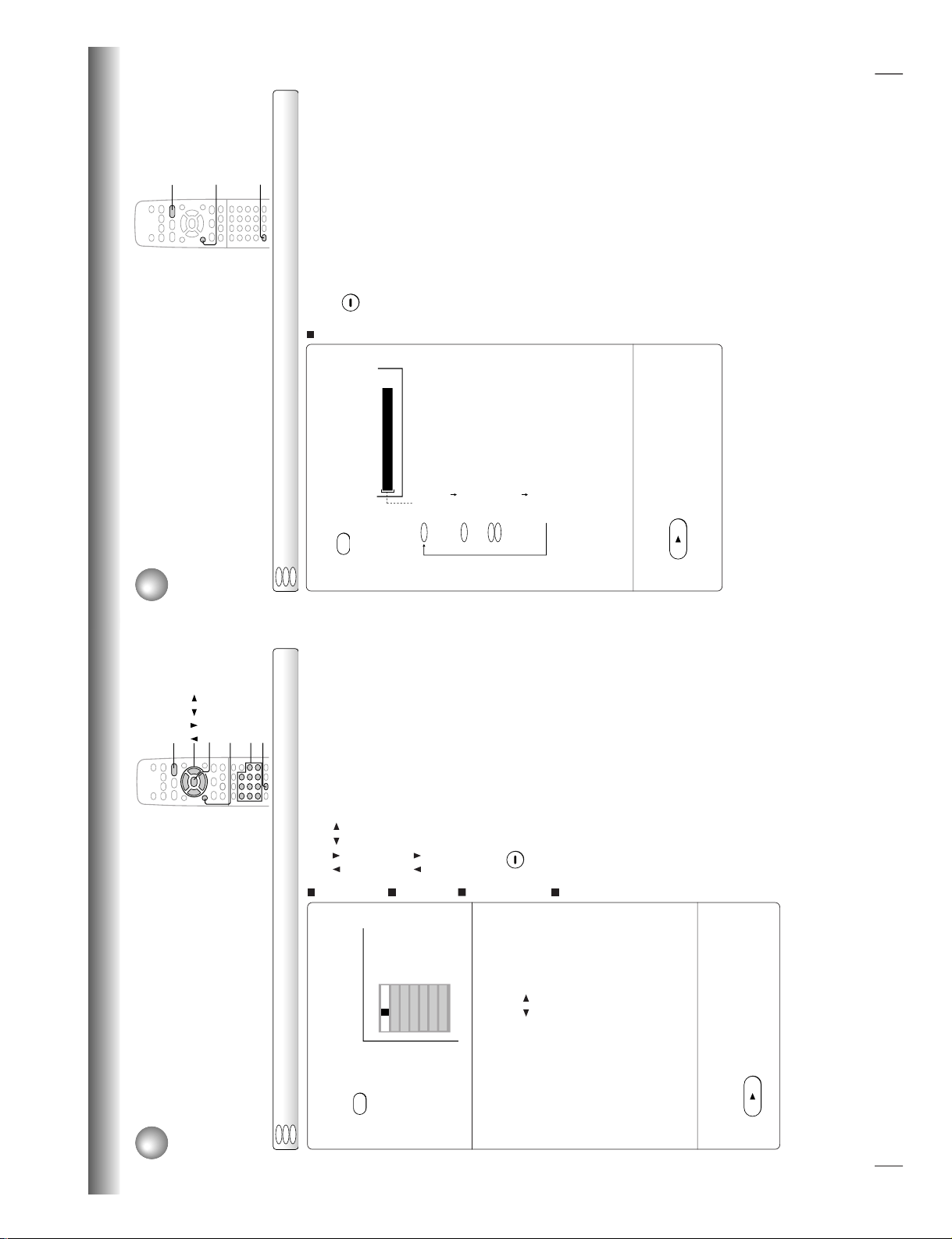
This section shows you the basics on how to play a disc.
CAUTION
Keep your fingers well clear of the disc tray as it is closing.
Neglecting to do so may cause serious personal injury.
Basic playback
Preparations
• When you want to view a disc, turn on the TV and select the video input connected to the DVD video player.
• When you want to enjoy the sound of discs from the audio system, turn on the audio system and select the input connected
to the DVD video player.
1
2
OPEN/CLOSE
3
4
To start playback in the stop mode
Press PLAY.
PAUSE
PAUSE SKIP
OPEN/CLOSE
ON/STANDBY
PLAYSTOP
1
2
,
4
PLAY
3
STOP
ON/STANDBY indicator
DVD display
Press ON/STANDBY.
The DVD video player turns on and
the color of the ON/STANDBY
indicator changes from red (standby)
to green (on).
When the DVD video player is turned on for
the first time, a message appears. Press
ENTER, and make the proper settings before
proceeding to step 2.
45
Press OPEN/CLOSE.
The disc tray opens.
Place the disc on the disc tray.
With the playback
side down
• There are two different disc sizes. Place the disc in
the correct guide on the disc tray. If the disc is out of
the guide, it may damage the disc and cause the
DVD video player to malfunction.
• Do not place a disc which is unplayable in this DVD
video player.
OPEN/CLOSE
Press OPEN/CLOSE to close the disc
tray.
Playback starts.
If you insert a DVD video disc that contains a top
menu, a menu may appear. See “Locating a title
using the top menu.”
24
• You may need to press the TOP MENU or MENU
button to display disc menu (depending on the actual
DVD video disc.)
DVD
VCD
CD
PLAY
21
Basic playback
To pause playback (still mode)
Press PAUSE/STEP during playbac k.
To resume normal playback, press
the PLAY button.
• Sound is muted during still mode.
To stop playback
Press STOP.
To remove the disc
Press OPEN/CLOSE.
Remove the disc after the disc tray
opens completely.
Be sure to press the OPEN/CLOSE button to close
the disc tray after you remove the disc.
PAUSE/STEP
STOP
OPEN/CLOSE
About the screen saver
If you pause a picture of a DVD video disc and leave it
still for a long while, the screen saver of the DVD video
player automatically appears (when “Screen Saver” is
set to “On”
43
). To turn off the screen saver, press the
PLAY button.
Automatic Power Off function
If the DVD video player is stopped, or the screen saver
is engaged for approximately 20 minutes, the DVD
video player will automatically turn itself off.
PAUSE/STEP
ENTER
MENU
STOP
TOP MENU
PLAY
2, 4
1
/
Notes
• Do not move the DVD video player during playback. Doing so may damage the disc.
• Use the OPEN/CLOSE button to open and close the disc tray. Do not push the disc tray while it is moving. Doing so may
cause the DVD video player to malfunction.
• Do not push up on the disc tray or put any objects other than discs on the disc tray. Doing so may cause the DVD video
player to malfunction.
• In many instances, a menu screen will appear after playback of a movie is completed. Prolonged display of an on-screen
menu may damage your television set, permanently etching that image onto its screen. To avoid this, be sure to press the
STOP button on your remote control once the movie is completed.
To obtain a higher quality picture
Occasionally, some picture noise not usually visible during a normal broadcast
may appear on the TV screen while playing a DVD video disc because the high
resolution pictures on these discs include a lot of information. While the amount of
noise depends on the TV you use with this DVD video player, you should generally
reduce the sharpness adjustment on your TV when viewing DVD video discs.
About
DVD VCD
CD
The
DVD
VCD CD
icons on the heading bar show the playable discs for the
function described under that heading.
DVD
: You can use this function with DVD video discs.
VCD
: You can use this function with VIDEO CDs.CD : You can use this function with audio CDs.
1-10
Page 15
22
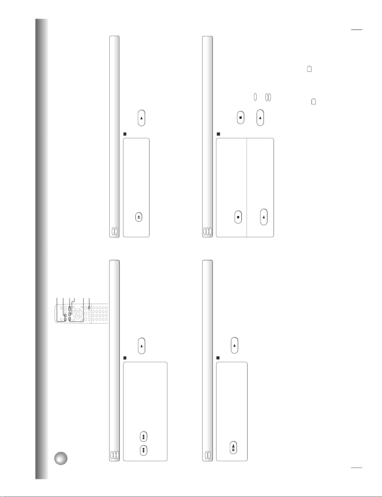
Basic playback
Playing a Disc (continued)
You can play discs at various speeds, and resume playback from the location
where you stopped playback.
Playing in fast reverse or fast forward directions
Press REV or FWD during playback.
REV: Fast reverse playback
FWD: Fast forward playback
Each time you press the REV or
FWD button, the playback speed
changes.
To resume normal playback
Press PLAY.
Notes
• The DVD video player mutes sound and omits subtitles
during reverse and forward scan of DVD video discs.
However, the DVD video player plays sound during fast
forward or fast reverse play of audio CDs.
• The playback speed may differ depending on the disc.
Playing frame by frame
Press PAUSE/STEP during still playback.
Each time you press the PAUSE/
STEP button, the picture advances
one frame.
To resume normal playback
Press PLAY.
Note
The sound is muted during frame by frame playback.
FWD
REV
PAUSE/STEP
PLAY
SLOW
STOP
DVD
VCD
REV
FWD
PLAY
PAUSE/STEP
PLAY
DVD
VCD
CD
23
Basic playback
Press STOP at the location where you
want to interrupt playback.
The DVD video player memorizes
the location where playback is
stopped.
Press PLAY.
The DVD video player resumes
playback from the location where
you stopped playback.
Playing in slow-motion
Press SLOW during playback.
Each time you press the SLOW
button, the slow-motion speed
changes.
To resume normal playback
Press PLAY.
Notes
• The sound is muted during slow-motion playback.
• The playback speed may differ depending on the disc.
Resuming playback from the same location
1
2
To start playback from the beginning regardless
of the location where you stopped playback
1 Press STOP twice.
The DVD video player’s memory is
cleared.
2 Press PLAY.
Playback starts from the
beginning of the current title.
Playback starts from the
beginning of the disc.
• If you want to return to the beginning of a DVD video
disc, open and close the disc tray once with the
OPEN/CLOSE button before pressing the PLAY
button.
Notes
• The DVD video player’s memory is also cleared when:
–you change the parental lock setting
43
or select a disc
menu language
41
.
–you open the disc tray.
• There may be a difference in the location where playback
resumes depending on the disc.
• Settings you changed using the on-screen displays while the
DVD video player keeps a location in the memory may
function only after the memory is cleared.
DVD
VCD
DVD
VCDCDDVD
SLOW
PLAY
STOP
PLAY
STOP
PLAY
VCD
CD
1-11
Page 16
24
Basic playback
Locating a Specific Title, Chapter, or Track
Normally, DVD video discs are divided into titles, and the titles are sub-divided into chapters. VIDEO CDs and audio CDs
are divided into tracks. You can quickly locate any specific title, chapter, or track.
Locating a title using the top menu
Press TOP MENU.
The top menu appears on the TV
screen.
e.g.
Press
/ / / to select the title you
want.
If the titles in the top menu are
assigned a number, you can directly
locate a specific title by pressing its
designated number with the number
buttons.
Press ENTER.
Playback starts from chapter 1 of the
selected title.
1
2
DVD video disc
Title 1
Title 2
Chapter 1 Chapter 2 Chapter 1 Chapter 2 Chapter 3
Track 1
Track 2 Track 3 Track 4 Track 5
VIDEO CD/audio CD
3
Notes
• The instructions above describe basic procedures which
may vary depending on the contents of the DVD video disc.
If different instructions appear on the TV screen, follow those
instructions.
• If you display the top menu during playback and press the
TOP MENU button again without selecting any title, the DVD
video player may resume playback from the point where you
first pressed the TOP MENU button (depending on the actual
DVD video disc.)
• This method of locating a title is available only on a disc that
contains a top menu.
• Instruction notes of discs may refer to the button that
displays the top menu as TITLE button.
Locating a title by entering the title number
Press T .
Make sure that the space of “T (Title)”
is highlighted.
(You can shift the highlight using the
/
buttons.)
Enter the number for the title you want,
using
/ or the number buttons.
e.g. To select title 2
To select title 12
Press PLAY.
Playback starts from chapter 1 of the
selected title.
1
3
Notes
• Pressing the CLEAR button resets the title and chapter
numbers. To clear the “T (Title)” and “C (Chapter)” display,
press the T button several times.
• This method of locating a title is available only on a disc that
contains title numbers.
DVD
TOP MENU
TITLE 1
TITLE 3
TITLE 2
TITLE 4
ENTER
ENTER
DVD
T
SEARCH
2
2
21
PLAY
1
–
:
––
:
––
1
e.g.
25
Basic playback
Locating a specific chapter or track directly
Press T .
If you are using a VIDEO CD/audio CD, skip steps 1
and 2, then at steps 3, enter the number for the track
you want using the number buttons.
Press to highlight the space of “C
(Chapter).”
Enter the number for the chapter or
track you want, using
/ or the
number buttons.
When you use the number buttons, you can use
the +10 button to select numbers from 10 through
99.
e.g. To select chapter or track 25
or
1
2
Press PLAY.
Playback starts from the selected
chapter or track.
3
4
To select a title and chapter number at the same
time
Perform step 1, and enter a title number you want in the
space of “T (Title)” using the number buttons or the
/
buttons then perform steps 2 to 4.
Note
Pressing the CLEAR button resets the title and chapter
numbers. To clear the “T (Title)” and “C (Chapter)” display,
press the T button several times.
Locating a specific chapter or track
Press SKIP
or repeatedly to display
the chapter or track number you want.
Playback starts from the selected chapter or track.
To locate succeeding chapters or tracks
Playback starts from the beginning of
the current chapter or track.
When you press twice, playback starts
from the beginning of the preceding
chapter or track.
Notes
• Some titles may not display chapter numbers.
• If you press and hold the SKIP
or button on the front
panel during playback, the DVD video player performs fast
reverse or fast forward playback. You can vary the speed by
pressing the button repeatedly.
To locate chapters or tracks during fast reverse or fast
forward playback, first press the PLAY button to resume
normal playback, then use the SKIP
or button.
• When you set “Title Stop” to “Off”
45
, you can access
chapters in another title. If you go back to the preceding title
by pressing the SKIP
button, the DVD video player
locates the first chapter of the title. When “Title Stop” is set
to “On,” you can access chapters only within the current title.
T
SEARCH
ENTER
PLAY
DVD
VCD
CD
SKIP
SKIP
/ / /
CLEAR
PLAY
ENTER
TOP MENU
T
Number buttons
SKIP
5
+10 +10
DVD
VCD
CD
52
1
–
:
––
:
––
1
1
–
:
––
:
––
1
e.g.
e.g.
1-12
Page 17

26
Advanced playback
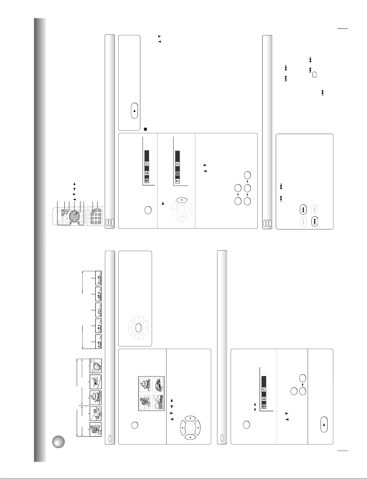
Press T three times.
You may have to press further
depending on the disc. Press the
button repeatedly until the clock icon
is highlighted.
Press the number buttons to enter the
time.
Press PLAY.
Playback starts from the desired
location.
Accessing a Specific Location Directly
You can access a specific location by entering its corresponding time (hours,
minutes, seconds).
Entering the time of the desired location
2
1
Notes
• Some discs may not respond to this process.
• Some scenes may not be located precisely as you specified.
• This method for accessing specific locations is available
only within the current title of the DVD video disc or within
the current track of the VIDEO CD/audio CD.
2
1
3
T
SEARCH
e.g.
3
PLAY
DVD
VCD
CD
1 2
5 3 0
1
–
:
––
:
––
1
1
1
:
25
:
30
1
e.g.
27
Advanced playback
Playing Repeatedly
You can play a specific title, chapter, track, or segment repeatedly.
(Title repeat, chapter/track repeat, A-B repeat)
Repeating a title, chapter, or track
Press REPEAT.
Each time you press the REPEAT
button, the repeat mode changes as
follows.
1
To resume normal playback
Press CLEAR.
Note
Some discs may not permit repeat operation.
Repeating a specific segment
Press A-B RPT at the beginning of the
segment (point A) you want to play
repeatedly.
Press A-B RPT again at the end of the
segment (point B).
The DVD video player automatically
returns to point A and starts repeat
playback of the selected segment
(A-B).
2
1
To resume normal playback
Press CLEAR.
Notes
• Some discs may not permit A-B repeat operation.
• You cannot set the A-B repeat function for a segment that
includes multiple camera angles
33
.
• You can specify a segment only within the current title or
track (VIDEO CD).
• There may be a slight difference between point A and the
location where playback actually resumes depending on the
disc.
A-B RPT
REPEAT
CLEAR
PLAY
A-B RPT
A-B RPT
REPEAT
CLEAR
CLEAR
Press PLAY.
The DVD video player starts repeat
playback.
Press the PLAY button within about
5 seconds after you press the
REPEAT button.
2
PLAY
DVD
VCD
CD
DVD
VCD
CD
DVD
DVD
DVD
VCD
CD
VCD
CD
Chapter Repeat
Title Repeat
Track Repeat
All Repeat
Repeat Off
Repeats the current
chapter.
Repeats the current
title.
Repeats the current
track.
Repeats the entire
disc.
Resumes normal
playback.
Chapter Repeat
A–
A–B
1-13
Page 18
28
Advanced playback
Playing in a Favorite Order
You can combine your favorite titles, chapters, or tracks and play them in the
order you determine. You can program up to 30 selections into the memory.
(Memory playback)
Setting titles, chapters, or tracks in a favorite order
Insert a disc and press MEMORY during
stop.
The following display appears.
Select the items in the order you want
by pressing the number buttons, then
ENTER for each item.
Each time you press the
/ button, the space
of “T” and “CT” is highlighted in turn. Highlight
where you want to enter, then press the
corresponding number buttons.
To select another chapter in the same title, you do
not need to select the title number.
To select tracks from a VIDEO CD/audio CD in
order, press the number buttons for the track,
then press the ENTER button for each selection
you want.
Note
The space of “T (Title)” may be sho wing a number.
Neglect this number when using a VIDEO CD/audio
CD.
Press PLAY while the display appears
on the TV screen.
The DVD video player starts
memory playback.
1
2
3
To change the programmed selections
1 While the display appears on the TV screen, press
/ / / to move the highlighted bar to the item
you want to change.
2 Change the selection following the instructions in
step 2.
To cancel the programmed selections
1 While the display appears on the TV screen, press
/ to move the highlighted bar to the item you
want to cancel.
2 Press CLEAR.
To resume normal playback from memory
playback
Press CLEAR.
The memory playback indicator
disappears.
To program during playback
If you press the MEMORY button during playback, a
programming display appears.
Follow steps 2 and 3.
Notes
• Some discs may not permit memory playback operation.
• If you press the REPEAT button during memory playback,
the DVD video player repeats the current memory playback.
• If you press the MEMORY or RETURN button while the
display appears on the TV screen, the display disappears.
• The programmed selections will be cleared when you turn
off the DVD video player.
T: Title number
CT: Chapter number
or track number
MEMORY
PLAY
CLEAR
DVD
VCD
CD
/ / /
CLEAR
2
2
1
3
2
T
:
--
CT
:
---
1
T
:
--
CT
:
---
3
T
:
--
CT
:
---
4
T
:
--
CT
:
---
5
T
:
--
CT
:
---
6
T
:
--
CT
:
---
7
T
:
--
CT
:
---
e.g.
29
Advanced playback
Playing in Random Order
You can play titles, chapters within a title, or tracks in random order .
(Random playback)
Playing titles, chapters or tracks in random order
Press RANDOM.
Each time you press the RANDOM
button, the random playback mode
changes as follows.
2
1
To resume normal playback
Press CLEAR.
Notes
• Some discs may not permit random playback operation.
• You cannot use the random playback function in conjunction
with the memory playback function.
CLEAR
2
1
CLEAR
RANDOM
PLAY
DVD
VCD
CD
If you press the RANDOM button
during playback, the DVD video
player automatically starts random
playback after finishing the current
title, chapter or track.
Press PLAY.
The DVD video player starts random
playback.
Press the PLAY button within about
5 seconds after you press the
RANDOM button.
DVD
DVD
VCD
CD
Chapter Random
Title Random
Track Random
Random Off
Plays chapters within
the current title in
random order.
Plays titles in random
order.
Plays tracks in
random order.
Resumes normal
playback.
Chapter Random
1-14
Page 19
30
Advanced playback
Zooming a Picture
You can magnify areas within a picture.
Zooming a picture
/ / /
ZOOM
CLEAR
ENTER
DVD
Press ZOOM during normal, slow or still
playback.
The DVD video player enters the
zoom playback mode and displays
the icon.
: As you repeatedly press the ENTER
(or ZOOM) button while “ZOOM” is
selected, the magnification level
changes.
Variation of the levels includes
reducing.
: If you press the ENTER button while
“EXIT” is selected, you can turn off
the icon, keeping the current
magnification level.
You can shift the highlight within the
icon by the
/ / /
buttons.
If you press and hold the
/ / /
buttons, the zoom point shifts.
Pressing the CLEAR button restores
the zoom point to the center of the
picture.
To resume normal playback
While “ZOOM” is selected, press ZOOM repeatedly to
turn off the icon.
Picture restores the size when the icon disappears.
• The ENTER button cannot cancel zoom playback if
you have turned off the icon by selecting “EXIT.” To
restore normal picture size, press the ZOOM button
to display the icon, then further press the ZOOM
button until the icon turns off.
Notes
• Some discs may not respond to zoom feature.
• During some scenes, the buttons may not work as described.
• Zooming does not work on subtitles or menus included on
DVD video discs.
• While the icon is displayed, the
/
/ / buttons cannot
work on menus included on DVD video discs. If you want to
view the menus, turn off the icon.
• The magnification level varies depending on the picture size
you select.
40
ZOOM
ENTER
ZOOM
CLEAR
e.g.
31
Advanced playback
Light :
Brighter than in “Normal”.
Normal:
Standard black level.
Movie 1:
To raise brightness to clarify details.
Movie 2:
To deepen colors.
Animation:
To raise contrast enhancing colors.
Selecting the Picture Enhancement (E.P.M.*)
You can easily switch the picture enhancement to your preference.
*E.P.M.: Enhanced Picture Mode
ENTER
2
1, 2
Selecting the picture enhancement
Press E.P.M.
The picture enhancement selection
appears.
2
1
To turn off the picture enhancement selection
Press ENTER.
Alternatively leave the DVD video
player unoperated for about 5
seconds after having made the
selection.
Note
Actual effects to pictures may vary depending on the TV.
Make the selection to your preference.
Select the picture enhancement by
pressing E.P.M. or
/
.
Each time you press the button, the picture
enhancement changes.
E.P.M.
ENTER
DVD
VCD
CD
1-15
Page 20
32
Advanced playback
Normal:
Normal sound.
3D (N-2-2):
To obtain expansive virtual surround
sound effects from just two speakers.
Dialogue:
To control dynamic range to make
dialogues easier to hear (only when
playing a DVD video disc recorded
on the Dolby Digital recording
system).
• To use this enhancement on
sounds output from the
BITSTREAM/PCM (DIGITAL)
AUDIO OUT jack, be sure to set
“Audio Out Select” to “PCM”.
40
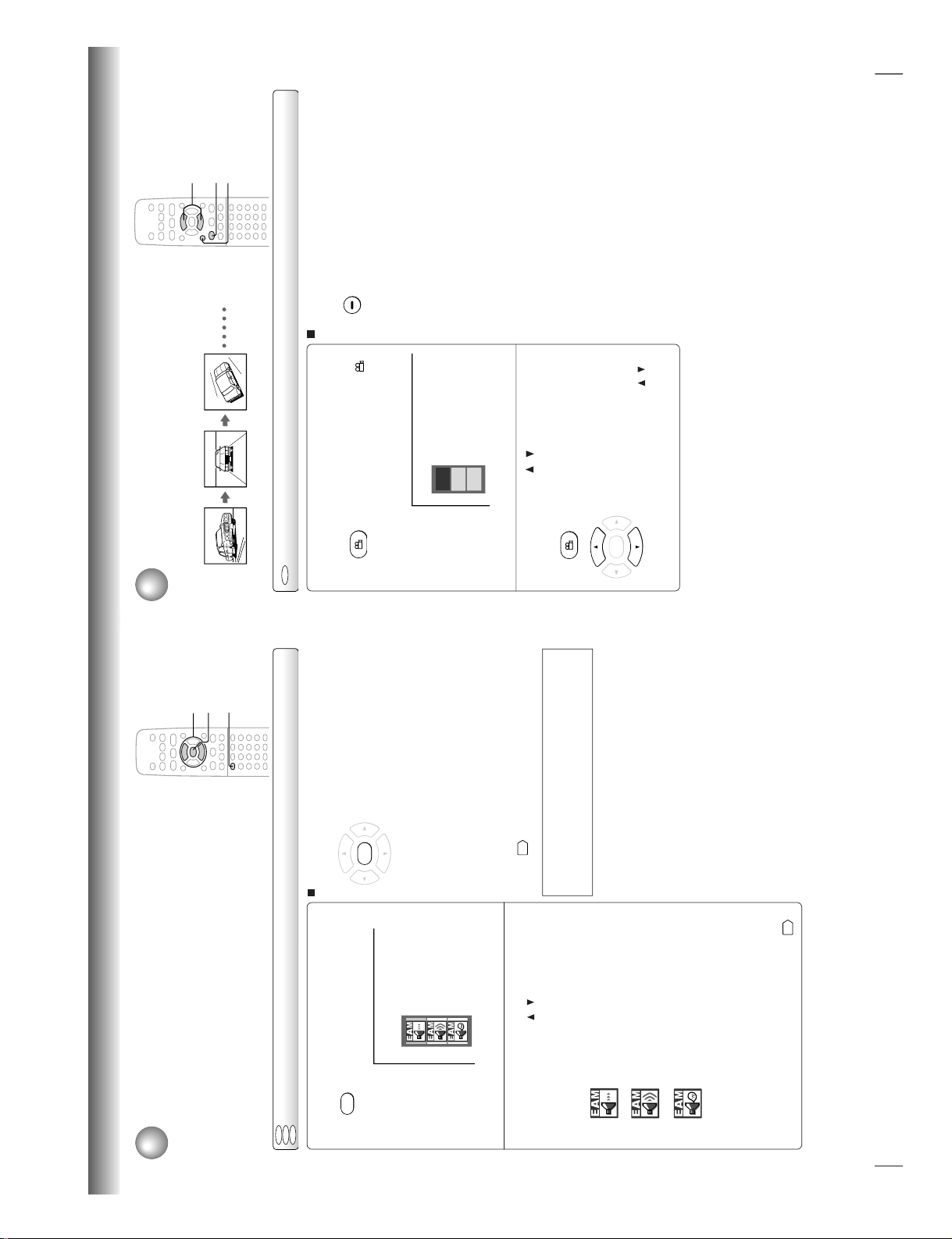
Selecting the Sound Enhancement (E.A.M.*)
You can easily switch the sound enhancement to your preference.
*E.A.M.: Enhanced Audio Mode
ENTER
2
1, 2
Selecting the sound enhancement
Press E.A.M.
The sound enhancement selection
appears.
Select the sound enhancement by
pressing E.A.M. or
/ .
Each time you press the button, the sound
enhancement changes.
2
1
To turn off the audio enhancement selection
Press ENTER.
Alternatively leave the DVD video
player unoperated for about 5
seconds after having made the
selection.
Notes
• Actual effects to sounds may vary depending on the
speakers. Make the selection to your preference.
• Actual effects to sounds may vary depending on the disc.
• When the DVD video player is connected to an amplifier
equipped with Dolby Pro Logic Surround, select “Normal”.
Otherwise, Dolby Pro Logic Surround may function
differently than usual.
• Selecting “Dialogue” disables “Dynamic Range Control”
function
40
.
E.A.M.
ENTER
Spatializer
®
3-Dimensional Sound Processing provided by Desper
Products. Inc.
Certain audio features of this product manufactured under a license
from Desper Products, Inc., Spatializer
®
and the circle-in-square
device are trademarks owned by Desper Products, Inc.
DVD
VCD
CD
33
Advanced playback
Selecting the Camera Angle
If the scene was recorded from multiple angles, you can easily change
the camera angle of the scene you are watching.
Changing the camera angle
Press ANGLE while playing a scene
recorded with multiple angles.
While playing a scene recorded with
multiple angles, the angle icon (
)
flashes in the DVD display.
Press the ANGLE button while the
angle icon is flashing.
Press ANGLE or
/ while the angle
number is displayed on the TV screen.
Each time you press the ANGLE
button, the camera angle changes.
You can change the camera angle
directly by pressing the number
buttons corresponding to its angle
number instead of using the
/
buttons.
To turn off the angle number display
Press CLEAR.
Notes
• You can change the camera angle during still playback. The
camera angle changes to the new setting when you resume
normal playback.
• If you pause a picture immediately after changing a camera
angle, the resumed playback picture may not display the new
camera angle.
1
2
2
1, 2
CLEAR
DVD
ANGLE
ANGLE
ENTER
CLEAR
1
2
3
e.g.
1-16
Page 21
34
Advanced playback
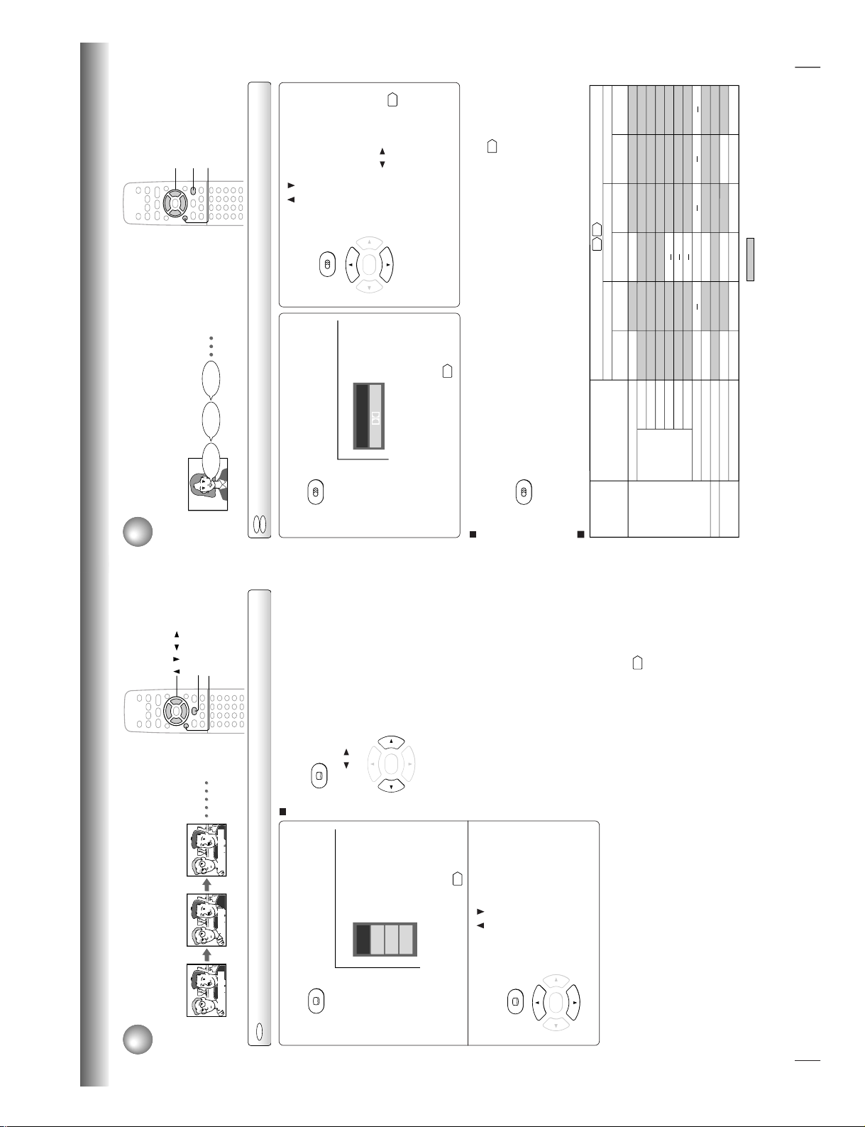
Selecting Subtitles
You can display subtitles on the TV screen and select a subtitle language
from those included on the DVD video disc.
Selecting a subtitle language
Press SUBTITLE during playback.
The current subtitle setting is
displayed.
The abbreviation of the language appears instead
of the language name. Refer to the list of
languages and their abbreviations.
46
Press SUBTITLE or
/
while the subtitle
setting is displayed on the TV screen.
Each time you press the SUBTITLE
button, the subtitle languages
included on the DVD video disc
change.
To turn off the subtitle setting display,
press the CLEAR or ENTER button.
To turn subtitles on or off
1 Press SUBTITLE during playback.
2 Press
/ while the subtitle setting is displayed on
the TV screen, to select “On” or “Off.”
Notes
• When you turn on the DVD video player or replace a disc, the player returns to the initial default setting
42
.
When you select a subtitle language which is not included on the disc, the DVD video player plays a prior language
programmed on the disc.
• During some scenes, the subtitles may not appear immediately after you change the subtitle language.
1
2
Notes
• Some DVD video discs are set to display subtitles
automatically, and you cannot turn them off even if you set
the subtitle function to off.
• During some scenes, the subtitles may not appear
immediately after you select “On.”
• Some DVD video discs will allow you to make subtitle
selections and turn subtitles on or off only via the disc menu.
SUBTITLE
/ / /
CLEAR
DVD
SUBTITLE
SUBTITLE
SUBTITLE
ENTER
ENTER
Bonsoir!Good evening! `Buenas tardes!
Off
JP
N
1
FRE 1
SP
A
1
e.g.
35
Advanced playback
Press AUDIO or
/ while the audio
setting is displayed on the TV screen.
Each time you press the AUDIO
button, the audio settings included
on the DVD video disc change.
If you press the
/ buttons, you
can select output sound format.
40
To turn off the audio setting display, press the
CLEAR button.
Selecting a Language
You can select a preferred language and sound recording system from those
included on the DVD video disc.
Selecting a playback audio setting
Press AUDIO during playback.
The current audio setting is
displayed.
The abbreviation of the language appears instead
of the language name. Refer to the list of
languages and their abbreviations.
46
Output sound conversion table (sampling frequency/quantization bit)
12
CLEAR
2
1, 2
DVD
VCD
AUDIO
AUDIO
ENTER
Good morning!
¡Buenos días!
Bonjour!
BITSTREAM/PCM
jack
ANALOG AUDIO
OUT jacks
BITSTREAM/PCM
jack
ANALOG AUDIO
OUT jacks
BITSTREAM/PCM
jack
ANALOG AUDIO
OUT jacks
“Bitstream” “Analog 2ch”
“PCM”
Audio selection from the menu
and output jacks on the rear panel
Recording system
Discs
DVD video
discs
Audio CDs
VIDEO CDs
Linear PCM
Dolby Digital
DTS
MPEG1, MPEG2
Linear PCM
44.1 kHz/16 bit
48 kHz/20 bit
48 kHz/16 bit
48 kHz/16 bit
48 kHz/16 bit
48 kHz/20 bit
48 kHz/24 bit
96 kHz/16 bit
96 kHz/20 bit
96 kHz/24 bit
48 kHz/16 bit
48 kHz/16 bit
48 kHz/16 bit
48 kHz/16 bit
48 kHz/16 bit
48 kHz/16 bit
48 kHz/16 bit
48 kHz/20 bit
48 kHz/24 bit
48 kHz/16 bit
48 kHz/20 bit
48 kHz/24 bit
Bitstream
Bitstream
Bitstream
Bitstream
44.1 kHz/16 bit
44.1 kHz/16 bit
Bitstream
Bitstream 48 kHz/16 bit 48 kHz/20 bit
48 kHz/16 bit
48 kHz/20 bit
48 kHz/24 bit
96 kHz/16 bit
96 kHz/20 bit
96 kHz/24 bit
48 kHz/16 bit
48 kHz/20 bit
48 kHz/24 bit
48 kHz/16 bit
48 kHz/20 bit
48 kHz/24 bit
48 kHz/16 bit
48 kHz/16 bit
48 kHz/16 bit
48 kHz/16 bit
48 kHz/16 bit
48 kHz/16 bit
44.1 kHz/16 bit44.1 kHz/16 bit
48 kHz/20 bit
44.1 kHz/16 bit44.1 kHz/16 bit
48 kHz/16 bit 48 kHz/16 bit 48 kHz/16 bit
MPEG1
44.1 kHz/16 bit
44.1 kHz/16 bit 44.1 kHz/16 bit
44.1 kHz/16 bit 44.1 kHz/16 bit 44.1 kHz/16 bit
4038
: 3D (N-2-2) sound enhancement can function.
DTS
(Noise)
Bitstream
(Noise)Bitstream
(Noise)
Bitstream
48 kHz/16 bit
48 kHz/16 bit
Selecting sound channels of VIDEO CDs
You can switch left and right channels by pressing the
AUDIO button repeatedly during playback.
Notes
• When you turn on the DVD video player or replace a disc,
player returns to the initial default setting
42
.
If you select a sound track which is not included on the disc,
the DVD video player plays a prior sound track programmed
on the disc.
• Some discs allow you to change audio selections only via
the disc menu. If this is the case, press the MENU button
and choose the appropriate language from the selections on
the disc menu.
ENG2
D 2CH
ENG
1
PCM
2CH
e.g.
AUDIO
1-17
Page 22
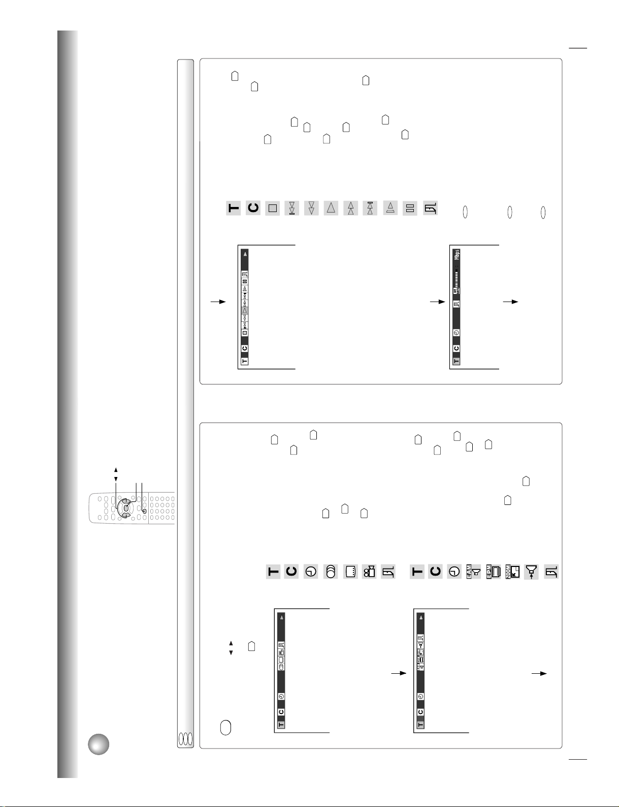
36
Advanced playback
Operating in the On-screen Display Mode
When you turn on the on-screen display, you can view information on operational
status and access the features and settings on-screen.
Press DISPLA Y.
The following display appears.
Each time you press the DISPLAY button, the on-screen display changes as follows.
If you press the
/ buttons to select an icon, then press the ENTER button, you can access the
feature.
When you select an icon (
*
), no need to press the ENTER button.
See the pages in
for details on the features.
Press DISPLA Y again.
Press DISPLA Y again.
DISPLAY
ENTER
/
DISPLAY
: Title number (Track number)
To locate a title or track using the number.
24
: Chapter number
To locate a chapter using the number.
25
: Elapsed time of the current title
To enter the time to locate a desired location.
26
: Audio setting 35: Subtitle setting
34
: Angle setting 33: To turn off the display.
: Title number (Track number)
To locate a title or track using the number.
24
: Chapter number
To locate a chapter using the number.
25
: Remaining time of the current title
T o enter the time to locate a desired location.
26
: E.A.M. (Enhanced Audio Mode) setting
32
: E.P.M. (Enhanced Picture Mode) setting
31
: To zoom a picture.
30
: “Audio Out Select” setting
40
BST: Bitstream 2CH: Analog 2ch PCM: PCM
: To turn off the display.
e.g. When playing a DVD video disc
3
0:08:162
(continued)
3 -0:21:282
Operating in the on-screen display mode
DVD
VCD
CD
*
*
*
*
*
*
37
Advanced playback
Press DISPLA Y again.
The on-screen display will vary depending on the disc.
: Data transfer rate (Mbit/s)
= Amount of picture, sound and subtitle data in the
DVD video disc transferred per second.
The larger the value is, the more data processed,
but this does not necessarily insure better picture
quality.
: CD-Text
Displays CD-Text data if included on the audio
CDs. (Some letters may not be displayed properly
depending on the disc.)
: The on-screen display turns off.
: Title number (Track number)
To locate a title or track using the number.
24
: Chapter number
To locate a chapter using the number.
25
: To stop playback. 21: Playback starts from the beginning of the
current chapter or track.
25
: Fast reverse playback 22: To start playback.
20
: Fast forward playback 22: To locate succeeding chapters or tracks. 25: To slow motion playback.
23
: To pause playback. 21: To turn off the display.
23
2 3
0
:
08
:
16
9.6
OFF
To turn off the on-screen display, press
DISPLAY again.
CD
DVD
VCD
*
*
1-18
Page 23

38
Function setup
Customizing the Function Settings
You can change the default settings to customize performance to your
preference.
Setting procedure
Press SETUP during stop.
The following on-screen display
appears.
Press
/ to select a symbol for the
setting you want to change.
(See the next page.)
Picture performance settings
Output sound settings
Language settings
Display settings
Operational settings
Initial settings
2
31
Notes
• The on-screen display disappears when you press the
SETUP button.
• The SETUP button can function even during normal
playback, however some operations may be inaccessible,
and a message will appear. In this case, try again after
playback is stopped.
Press
/ to select the setting you
want to change, then press ENTER.
Change the selection by
/ or other
buttons, by referring to the
corresponding pages
39
, then press
ENTER.
Repeat steps 3 and 4 to change other
settings.
To select another operation, go back to step 2.
Press SETUP.
The on-screen display disappears.
4
5
6
To return to the previous display
Press RETURN.
Picture
TV Shape
4:3 LB
A
B
C
PAL/Auto
Auto
A
B
C
DVD
VCD
CD
RETURN
2
1, 6
3, 4
SETUP
ENTER
ENTER
ENTER
ENTER
ENTER
SETUP
RETURN
39
Function setup
TV Shape
PAL/Auto
Audio Out Select
Dynamic Range Control
Karaoke Vocal
On-Screen Language
Disc Menu Language
Audio Language
Subtitle Language
On-Screen Displays
Background
Screen Saver
Pause/Still
Parental Lock
Title Stop
PBC
On-Screen Language
TV Shape
Audio Out Select
To select a picture size according to the aspect
ratio of your TV.
To select to the video system of a disc.
To select an output sound format corresponding
to your system connection.
To turn on or off a function that makes faint
sounds easier to hear even if you lower the
volume during late hours playback.
To turn on or off the vocal output during DVD
KARAOKE disc playback.
To select a preferred language for on-screen
displays.
To select a preferred language for disc menus.
To select a preferred language for the sound
track.
To select a preferred language for subtitles.
To turn on or de-activate the operational status
display on the TV screen.
To select the background color or background
picture.
To turn the screen saver on or off.
To select the resolution of still pictures.
(Field/Frame)
To turn the parental lock function on or off.
To turn on or off a feature that automatically
stops playback after a title has been viewed.
To use the menu screen when playing a PBC-
controllable VIDEO CD.
To install the initial system setting.
Setting Details
40
40
40
40
41
41
41
42
42
43
43
43
43
43
45
45
45
Page
DVD
DVD
DVD
VCD
CD
DVD
DVD
VCD
CD
DVD
DVD
DVD
DVD
VCD
CD
DVD
VCD
CD
DVD
DVD
DVD
DVD
VCD
DVD
VCD
CD
A
B
C
DVD
VCD
1-19
Page 24
40
Function setup
TV Shape
DVD
4:3 Letterbox: Select when a standard 4:3 TV is
connected.
Displays theatrical images with
masking bars above and below the
picture.
4:3 Normal: Select when a standard 4:3 TV is
connected.
Displays pictures cropped to fill
your TV screen. Either or both
sides of the picture are cut off.
16:9 Widescreen: Select when a 16:9 wide TV is
connected.
Notes
• The displayable picture size is preset on the DVD video
disc. Therefore, the playback picture of some DVD
video discs may not conform to the picture size you
select.
• When you play DVD video discs recorded in the 4:3
picture size only, the playback picture always appears
in the 4:3 picture size regardless of the TV shape
setting.
• If you select “16:9 Widescreen” and you own a 4:3 TV
set, the DVD playback picture will be horizontally
distorted during playback. Images will appear to be
horizontally compressed. Always be sure that your TV
shape conforms to the actual TV in use.
PAL/Auto
DVD
VCD
PAL: To play a PAL disc. Connect a PAL TV to view a
picture.
Auto:The DVD video player automatically identifies
PAL or NTSC video system of a disc. Connect
a multisystem TV (PAL/NTSC compatible) to
view a picture.
A playback picture may be distorted when
detected a signal change between PAL and
NTSC on the disc.
Setting details
Customizing the Function Settings (continued)
Audio Out Select
DVD VCD CD
Select the output sound format corresponding to your
system connection.
For details of sound recording systems, see
35
.
Bitstream: Select when connected to an amplifier
equipped with a Dolby Digital, DTS,
MPEG1 or MPEG2 decoder.
18
19
The DVD video player outputs digital
audio information in the bitstream
format when you play a DVD video disc
recorded on the Dolby Digital, DTS,
MPEG1 or MPEG2 recording system.
Analog 2ch: Select when connected to a TV, or
Dolby Pro Logic or stereo system via
the analog audio jacks.
16
17
18
PCM: Select when connected to a 2 channel
digital stereo amplifier.
19
The DVD video player outputs sounds
in the PCM 2ch format when you play a
DVD video disc recorded on the Dolby
Digital, MPEG1 or MPEG2 recording
system.
Dynamic Range Control
DVD
Off: Full dynamic range is maintained.
On: Dynamic range is reduced.
Notes
• This function works only during playback of Dolby
Digital recorded discs.
• The level of Dynamic Range Reduction may differ
depending on the DVD video disc.
Picture
TV Shape
4:3 LB
A
B
C
PAL/Auto
Auto
Audio
Dynamic Range Control
Karaoke Vocal
Audio Out Select
Bitstream
On
Off
A
B
C
41
Function setup
Karaoke Vocal
DVD
Off: The primary vocal is not output.
On: The primary vocal is output when it is recorded
on the disc.
Notes
• The vocal output feature is used during playback of
Dolby Digital (multi-channel) recorded DVD KARAOKE
discs. This feature allows you to turn off vocal audio
tracks, or restore them for background
accompaniment.
• When playing KARAOKE, connect appropriate audio
equipment such as an amplifier to the DVD video
player.
On-Screen Language
DVD VCD
CD
English: To view on-screen displays in English.
: To view on-screen displays in Chinese.
Disc Menu Language
DVD
English: To display disc menus in English.
Chinese: To display disc menus in Chinese.
Others: To make a further choice.
After pressing the ENTER button, follow
steps 1) - 4) below.
1) Obtain the abbreviation of the preferred
language from the list
46
.
2) Select the first character by pressing the
/
buttons.
3) Press the
/ buttons to shift and select the
second character by pressing the
/
buttons.
4) Press the ENTER button.
Note
Some DVD video discs may not include your pre-
selected language. In this case, the DVD video player
automatically displays disc menus consistent with the
disc’s initial language setting.
A
B
C
Language
Disc Menu Language
Audio Language
Subtitle Language
On-Screen Language
ENG
ENG
ENG
– – –
A
B
C
Language
Disc Menu Language
Audio Language
Subtitle Language
On-Screen Language
ENG English
Chinese
Others
Code
E
S
ENG
ENG
– – –
A
B
C
1-20
Page 25
42
Function setup
Customizing the Function Settings (continued)
Setting details
3) Press the
/ buttons to shift and select the
second character by pressing the
/
buttons.
4) Press the ENTER button.
Notes
• Some DVD video discs may be set to display subtitles
in a different language than you selected. A prior
subtitle language may be programmed on the disc.
• Some DVD video discs allow you to change subtitle
selections only via the disc menu. If this is the case,
press the MENU button and choose the appropriate
subtitle language from the selection on the disc menu.
Audio Language
DVD
English: To play sound tracks in English.
Chinese: To play sound tracks in Chinese.
Others: To make a further choice.
After pressing the ENTER button, follow
steps 1) - 4) below.
1) Obtain the abbreviation of the preferred
language from the list
46
.
2) Select the first character by pressing the
/
buttons.
3) Press the
/ buttons to shift and select the
second character by pressing the
/ buttons.
4) Press the ENTER button.
Note
Some DVD video discs may be played in a different
language than you selected. A prior language may be
programmed on the disc.
Subtitle Language
DVD
English: To display subtitles in English.
Chinese: To display subtitles in Chinese.
No Subtitle: To disable subtitles.
Others: To make a further choice.
After pressing the ENTER button,
follow steps 1) - 4) below.
1) Obtain the abbreviation of the preferred
language from the list
46
.
2) Select the first character by pressing the
/
buttons.
Language
Disc Menu Language
Audio Language
Subtitle Language
On-Screen Language
ENG English
Chinese
Others
Code
E
S
ENG
ENG
– – –
A
B
C
Language
Disc Menu Language
Audio Language
Subtitle Language
On-Screen Language
ENG English
Chinese
No Subtitle
Others
Code
A
A
ENG
ENG
– – –
A
B
C
43
Function setup
On-Screen Displays
DVD VCD CD
Off: Operational modes (e.g. “
”, “ ”) are not
displayed.
On: Operational modes (e.g. “
”, “ ”) are
displayed on-screen.
Background
DVD
VCD CD
Blue: Blue background.
Gray: Gray background.
Picture: To use the picture which appears when you
turn on the DVD video player as a
background.
Jacket: To use the jacket picture included on some
discs as a background. If it is not included,
a gray background will be substituted.
Screen Saver
DVD
Off: The screen saver is disengaged.
On: The screen saver operates.
Pause/Still
DVD
Auto: For normal use. Still and fast motion images
can be paused.
Frame: The resolution of still pictures is improved,
so that you can make a motionless picture
more clearer when you pause it.
Parental Lock
DVD
DVD video discs equipped with the parental lock
function are rated according to their content. The
contents allowed by a parental lock level and the way
a DVD video disc can be controlled may vary from
disc to disc. For example, if the disc allowed you
could edit out violent scenes unsuitable for children
and replace them with more suitable scenes, or lock
out playback of the disc altogether.
• DVD video discs may or may not respond to the
parental lock settings. This is not a defect in the DVD
video player. Make sure this function works with your
DVD video discs.
Off: The parental lock feature does not function.
After pressing the ENTER button, follow step 1)
below.
On: To activate the parental lock feature or change
the settings.
After pressing the ENTER button, follow steps
1) - 3) below.
Display
Background
Screen Saver
On-Screen Displays
On
Gray
On
A
B
C
Operation
Parental Lock
Title Stop
PBC
Pause/Still
Auto
Off
Off
On
A
B
C
Operation
Parental Lock
Title Stop
PBC
Pause/Still
Auto Off
Security Code
On
Off
Off
On
A
B
C
– – – –
(Continued)
1-21
Page 26
44
Function setup
Customizing the Function Settings (continued)
Setting details
(Continued)
1) Press the number buttons to create a personal
4-digit security code, then press the ENTER
button.
If you make a mistake before pressing the
ENTER button, press the CLEAR button and
enter your 4-digit security code again.
2) Enter the code of a country/area whose
standards were used to rate the DVD video
disc, referring to the list below.
a) Select the first character by pressing the
/ buttons.
b) Press the
/ buttons to shift and select
the second character by pressing the
/
buttons.
c) Press the ENTER button.
3) Press the
/ buttons to select the parental
lock level, then press the ENTER button.
You cannot play DVD video discs rated higher than
the level you selected unless you cancel the parental
lock function.
For example, when you select level 7, discs rated
higher than level 7 are locked out and cannot be
played.
The parental lock level is equivalent to the following
USA movie ratings.
Level 7: NC-17
Level 6: R
Level 4: PG 13
Level 3: PG
Level 1: G
The parental lock levels for other countries/areas
than U.S. are included for future use. Check the
appropriate parental lock level when you buy a DVD
video disc equipped with the parental lock feature in
the future.
To change the parental lock level
Follow steps 1) - 3).
To change your 4-digit security code
1) After selecting “On” or “Off,” press the STOP
button four times, then press the ENTER
button.
The 4-digit security code is cleared.
2) Press the number buttons to create a new
4-digit security code.
3) Press the ENTER button.
Code
AUBECACNHK
DK
FI
FR
DE
ID
IT
JP
MYNLNO
PH
RU
SG
ES
SECHTH
GB
US
Country/Area
AUSTRALIA
BELGIUM
CANADA
CHINA
CHINA HONG KONG
DENMARK
FINLAND
FRANCE
GERMANY
INDONESIA
ITALY
JAPAN
MALAYSIA
NETHERLANDS
NORWAY
PHILIPPINES
RUSSIAN FEDERATION
SINGAPORE
SPAIN
SWEDEN
SWITZERLAND
THAILAND
UNITED KINGDOM
UNITED STATES
Operation
Parental Lock
Title Stop
PBC
Pause/Still
Auto
Area Code
Off
Off
On
A
B
C
U
S
Level
7
Off
On
STOP
STOP STOP STOP
ENTER
45
Function setup
Title Stop
DVD
Off: The DVD video player continues after playback
of a title is completed.
On: The DVD video player stops after playback of a
title is completed.
PBC
VCD
Off: When playing a VIDEO CD without using the
menu.
On: To use the menu when playing a PBC-featured
VIDEO CD.
Initial Setup
DVD VCD CD
1) Press the
/ buttons to select “On-Screen
Language,” and press the ENTER button.
2) Select a language pressing the
/ buttons,
and press the ENTER button.
See page
41
, “On-screen Language.”
3) Make your selection in the same manner as
step 1) then step 2).
See page
40
, “TV Shape.”
See page
40
, “Audio Out Select.”
Initial Setup
TV Shape
Audio Out Select
On-Screen Language
ENG
4:3 LB
Bitstream
A
B
C
ENTER
ENTER
ENTER
ENTER
1-22
Page 27
47
Others
Before Calling Service Personnel
Check the following guide for the possible cause of a problem before contacting service.
Symptoms and correction
Symptom
No power.
The DVD video player turned
off by itself.
No picture.
No sound.
The playback picture has
occasional distortion.
Brightness is unstable or
noises are present in the
playback pictures.
The DVD video player does
not start playback.
Playback does not follow the
course of the disc’s program.
Buttons do not work.
The remote control does not
work properly.
Cause
• The power plug is disconnected.
• The automatic power off function turned
the unit off.
• The TV is not set to receive DVD signal
output.
• The video cable is not connected securely.
• The equipment connected with the audio
cable is not set to receive DVD signal
output.
• The audio cable is not connected securely.
• The audio receiver or TV is turned off.
• The setting of output sound format is
incorrect.
• The disc is dirty.
• It is in fast forward or fast reverse
playback.
• The effect of copy protection.
• No disc is inserted.
• An unplayable disc is inserted.
• The disc is placed upside down.
• The disc is not placed within the guide.
• The disc is dirty.
• The parental lock function is set.
• It is in the mode of repeat playback,
memory playback, etc.
• Power supply fluctuations or other
abnormalities such as static electricity may
interrupt correct operations.
• The remote control is not pointed at the
remote sensor of the DVD video player.
• The remote control is too far from the DVD
video player.
• The batteries in the remote control are
exhausted.
Correction
• Connect the power plug securely into the
wall outlet.
• Press the PLAY button.
• Select the appropriate video input mode
on the TV so the picture from the DVD
video player appears on the TV screen.
• Connect the video cable securely into the
appropriate jacks.
• Select the correct input mode of the
audio receiver so you can listen to the
sound from the DVD video player.
• Connect the audio cable securely into the
appropriate jacks.
• Turn on the equipment connected with
the audio cable.
• Select the proper audio setting.
• Eject the disc and clean it.
• Sometimes a small amount of picture
distortion may appear. This is not a
malfunction.
• Connect the DVD video player directly to
the TV. Avoid connecting the DVD video
player to a VTR or TV/VTR combination.
• Insert a disc.
• Insert a playable disc. (Check the disc
type and color system.)
• Place the disc with the playback side
down.
• Place the disc correctly inside the guide
on the disc tray .
• Clean the disc.
• Cancel the parental lock function or
change the parental lock level.
• These operations may prevent a proper
progress of the contents.
•
Turn the power on or off with the ON/
STANDBY button. Or disconnect the power
plug and insert it into the wall outlet again.
• Point the remote control at the remote
sensor of the DVD video player.
• Operate the remote control within about
7 m.
• Replace the batteries with new ones.
Page
16
21
20
16, 172016, 17
18, 192035, 38
40
9
–
16
201020
20
9
38, 43
–
–
15
15
15
46
Others
Table of Languages
Table of languages and their abbreviations
– – –
CHI (ZH)
DUT (NL)
ENG (EN)
FRE (FR)
GER (DE)
ITA (IT)
JPN (JA)
KOR (KO)
MAY (MS)
SPA (ES)
AAABAFAMARASAYAZBABEBGBHBIBNBOBRCACOCSCYDADZELEOETEUFAFIFJFOFYGAGD
GL
No alternate
language
Chinese
Dutch
English
French
German
Italian
Japanese
Korean
Malay
Spanish
Afar
Abkhazian
Afrikaans
Amharic
Arabic
Assamese
Aymara
Azerbaijani
Bashkir
Belorussian
Bulgarian
Bihari
Bislama
Bengali, Bangla
Tibetan
Breton
Catalan
Corsican
Czech
Welsh
Danish
Bhutani
Greek
Esperanto
Estonian
Basque
Persian
Finnish
Fiji
Faroese
Frisian
Irish
Scottish Gaelic
Galician
GNGUHAHIHRHUHYIAIEIKINISIWJIJWKAKKKLKMKNKSKUKYLALNLOLTLVMGMIMKMLMNMOMRMTMYNANENOOCOMORPAPL
PS
PTQURMRNRORURWSASDSGSHSISKSLSMSNSOSQSRSSSTSUSVSWTATETGTHTITKTLTNTOTRTSTTTWUKURUZVIVOWOXHYO
ZU
Guarani
Gujarati
Hausa
Hindi
Croatian
Hungarian
Armenian
Interlingua
Interlingue
Inupiak
Indonesian
Icelandic
Hebrew
Yiddish
Javanese
Georgian
Kazakh
Greenlandic
Cambodian
Kannada
Kashmiri
Kurdish
Kirghiz
Latin
Lingala
Laotian
Lithuanian
Latvian, Lettish
Malagasy
Maori
Macedonian
Malayalam
Mongolian
Moldavian
Marathi
Maltese
Burmese
Nauru
Nepali
Norwegian
Occitan
(Afan) Oromo
Oriya
Panjabi
Polish
Pashto, Pushto
Portuguese
Quechua
Rhaeto-Romance
Kirundi
Rumanian
Russian
Kinyarwanda
Sanskrit
Sindhi
Sango
Serbo-Croatian
Singhalese
Slovak
Slovenian
Samoan
Shona
Somali
Albanian
Serbian
Siswati
Sesotho
Sundanese
Swedish
Swahili
Tamil
Telugu
Tajik
Thai
Tigrinya
Turkmen
Tagalog
Setswana
Tongan
Turkish
Tsonga
Tatar
Twi
Ukrainian
Urdu
Uzbek
Vietnamese
Volapük
Wolof
Xhosa
Yoruba
Zulu
Abbreviation
Language
Abbreviation
Language
Abbreviation
Language
1-23
Page 28

2. LOCATION OF MAIN PARTS AND MECHANISM PARTS
2-1. Location of Main Parts
Disc motor PC board Feed motor PC board
EU02 Power supply PC board
EU04 Power SW PC board
Loading motor PC board
EU01 Main PC board
EU03 Front display PC board
Fig. 1-2-1
1-24
Page 29

2-2. Location of Mechanism Parts
y
y
r
Tra
Clamper sta
Fig. 1-2-2 Mechanism chassis assembly (Top side)
Loading moto
PC board
Mechanism chassis
Fig. 1-2-3 Mechanism chassis assembly (Bottom side)
1-25
Page 30

Loading belt
r
r
r
r
Gea
Kick lever
Loading motor
Disc motor
Gea
Gea
Cam Slide
Fig. 1-2-4 Mechanism chassis assembly (Internal side)
1-26
Page 31

r
r
r
r
d
<Type A>
Note:
When servicing, note that this model has two types of the
pickup mechanism assembly.
For the SD-1300A/H/T/Y, only Type A is a service part. Type B
can be changed to Type A pickup free from any performance
problem.
Front damper
Rack gear
assembly
Gear A
Gear B assembly
Rear damper
Front dampe
Pickup assembly
Sub chassis
Rear dampe
Fig. 1-2-5 Pickup mechanism chassis assembly (Top side)
Fig. 1-2-6 Pickup mechanism chassis assembly (Bottom side)
1-27
Feed moto
Feed moto
PC boar
Page 32

<Type B>
r
r
r
r
d
Front damper
Rack gear
assembly
Gear A
Gear B assembly
Rear damper
Front dampe
Pickup assembly
Sub chassis
Rear dampe
Fig. 1-2-7 Pickup mechanism chassis assembly (Top side)
Fig. 1-2-8 Pickup mechanism chassis assembly (Bottom side)
1-28
Feed moto
Feed moto
PC boar
Page 33

3. TROUBLESHOOTING
3-1. Main Circuit
3-1-1. Servo System
(1) Initial Operation after Power ON
Power ON
Send each LSI hard RST
command and initial command.
Pickup head is positioned at
transmission initial position.
Is tray closed?
Pin 5 of CN502,
TCLS=L
Y
2
NG
Disc presence/absence and
disc judgement
Is a disc present?
Y
DVD or CD initial setting.
N
Tray close operation
Pin 126 of IC605: LDMP = H/L
Pin 127 of IC605: LDMN = L
Tray stops.
Pin 126 of IC605: LDMP = H
Pin 127 of IC605: LDMN = L
N
Laser OFF
Display: INSERT DISC
Monitor screen: NO DISC
1
Is tray closed?
Pin 5 of CN502:
TCLS = L
Y
N
DVD single (single-layer)
DVD single
Initial setting.
DVD single
(single-layer)/DVD dual
(dual-layer)/CD?
DVD dual (dual-layer)
DVD dual
Initial setting.
To each disc playback process.
Fig. 1-3-1
1-29
CD
CD
Initial setting.
Page 34

1
Pickup (P.U.) transmission initial
operation does not occur.
The pickup transmission initial operation is carried out to
determine the initial position by transmitting the pickup to the
innermost position once (start-limit switch (pin 4 of CN503)
develops "L".) and to the external direction at low speed
(start-limit switch develops "H", turning off the switch.).
Does pulse of
1.65V 1.65V develop at
pin 162 of IC401?
Y
Check feed gear.
N
Check BUS between IC401
and IC605 and oscillation.
Fig. 1-3-2
2-1
"No disc" misjudgement display of
N
disc presence.
Does lens move with
UP/DOWN full stroke in
focus direction?
Y
N
3
Does focus search
voltage of 1.65V 0.4V develop
at pin 1 of IC503 (E537)?
Y
Does search signal
output at both edges of focus coil?
(Pins 15 to 18 of CN501)
Y
Check pickup head
and wiring.
Is laser current normal?
Y
Does RFSB signal
develop more than 0.3V?
Y
Check peripheral
circuit of IC605.
N
N
Check IC401.
Check IC502.
Fig. 1-3-3
N
Check IC502.
Lens cleaning.
Replace pickup head.
1-30
Page 35

2-2
Disc kind misjudgement
(Initial setting is NG.)
N
Check IC502.
Lens cleaning.
Replace pickup head.
lop I min
Check wiring for
pickup head.
Check pins 13, 14
and 15 of IC502
serial bus.
Check peripheral
circuits of IC502,
Q501, Q502.
To turn on each laser diode forcibly, press the following buttons on the remote controller.
DVD LD: ZOOM, 0, 3, 0, ZOOM
CD LD: ZOOM, 0, 3, 1, ZOOM
After checked the laser current, press POWER or OPEN/CLOSE button to turn it off.
CAUTION
The laser ray emitting out from the pickup head is very harmful to your eyes.
Keep your eyes from the objective lens at least 300mm distance during the pickup head operating.
When you perform solder removal work, please turn OFF a set power supply and perform the
ground of human body and a tool.
Are FE and RFSB
signals for each disc normal?
Y
Check peripheral
circuit of IC605.
Fig. 1-3-4
3
Check laser operating current.
Check laser current.
I min lop I max
Y
Check FE and RFSB signal
lop I max
lop 200 mA
Check solder removal
of the short land for
laser diode protection.
Laser operating current
min
typ max
DVD Iop
CD Iop
DVD Iop = Voltage between (E559 and E591) /10
CD Iop = Voltage between (E536 and E591) /10
Y
20mA
35mA
20mA
45mA
N
Replace pickup
mechanism.
80mA
80mA
W
W
DVD single (single-layer) disc
detection waveform
TP405 FE signal
TP503 RFSB signal
V : 500 mV/div
H : 2 ms/div
Fig. 1-3-6 Fig. 1-3-7 Fig. 1-3-8
1.65V
Fig. 1-3-5
DVD dual (dual-layer) disc
detection waveform
V : 500 mV/div
H : 2 ms/div
1-31
CD disc
detection waveform
V : 500 mV/div
H : 2 ms/div
Page 36

(2) Picture appears (PLAY)
PLAY
4
2-1
N
N
Disc motor (D.M.) forced
accelleration (500 ms)
Focus search
Is forcus servo
CLV servo ON.
Tracking balance adjustment
Tracking servo ON.
Focus gain adjustment
Tracking gain adjustment
Y
Y
Y
Y
Y
ON?
Repeat three times.
N
N
N
:
Automatic adjustment is carried
out when a disc is replaced after
power ON.
5
4
6
Focus balance adjustment
RF gain adjustment
N
N
Does NG continue
more than 3 s.?
Y
Disc playback NG
Is address code
possible to read?
Y
Search Picture appears.
Fig. 1-3-9
1-32
Page 37

4
FE signal
Pin 150 (TP405)
of IC401
RFSB signal
Pin 152 (TP503)
of IC401
0.3V
1.65V
0.3V
Focus search Focus servo on
Focus servo ON
signal waveform
Disc motor (D.M.) does not rotate.
Does pin 117 of IC401
(TP409) PLCK oscillate around
Check disc motor and wiring.
10 MHz ?
Y
Check peripheral circuits
of IC402.
N
Check peripheral
circuit of IC402.
Fig. 1-3-10
5
Focus servo is NG.
N
Are FE, RFSB,
FSON signals normal?
Do signals output to
pins 4 to 9 of CN501?
Y
Check IC502.
Fig. 1-3-11
Y
Check peripheral circuit of IC604.
N
Check wiring for
pickup head.
Lens cleaning.
Replace pickup
mechanism.
Fig. 1-3-12
1-33
Page 38

6
Tracking servo is NG.
Signal waveform at
tracking servo ON (CD)
Check IC502.
TE signal
Pin 151 (TP406) of IC401
1.65V
RFRP signal
Pin 153 (TP408) of IC401
N
Is TE signal normal?
Y
Check peripheral
circuit of IC604.
Fig. 1-3-13
Signal waveform at
tracking servo ON (DVD)
ON search Tracking servo on
Fig. 1-3-14
Search ON (SRCH)
Pin 38 (TP411) of IC401
Fig. 1-3-15
1-34
Page 39

7
Disc playback is NG (DVD).
Is PLL locked?
(Refer to waveforms.)
Y
Check signal process
system following to IC402.
N
Check peripheral circuits of
IC401 and IC604.
N
Fig. 1-3-16
Does pulse of
L = 1.65V and H = 3.3V
develop at pin 131 and
L = 0V and H = 1.65V
develop at pin 132
of IC401?
Y
Does RF output
higher than 1 V(p-p)
develop at pin 30 (TP502)
of IC502?
Y
Pin 43 of IC502 = 2.4V
Pin 44 of IC502 = 3.0V
Y
Check peripheral circuits
of IC502 and IC401.
N
Check peripheral circuits
of IC401 and IC604.
N
Check IC502.
Lens cleaning.
Pickup mechanism
replacement
DVD RF signal
Fig. 1-3-17
CD RF signal
DVD RF signal
Pin 30 (TP502) of IC502
V : 500 mV/div
H : 50 ns/div
CD RF signal
Pin 30 (TP502) of IC502
PLL works as a servo loop to generate a clock signal for reading RF
signal binary data. With the PLL locked, the eye pattern is identified
clearly when triggered with the read clock PLCK.
DVD playback waveform
DVD RF signal
Pin 30 (TP502) of IC502
DVD PLCK
Pin 117 (TP409) of IC401
CH1 : TP502 DVDRF 500 mV/div
CH2 : TP409 DVDPLCK 5 V/div
50 ns/div
Fig. 1-3-19
CD playback waveform
CD RF signal
Pin 30 (TP502) of IC502
Fig. 1-3-18
V : 500 mV/div
H : 100 ns/div
1-35
CH1 : TP502 CDRF 500 mV/div
CH2 : TP409 CDPLCK 5 V/div
100 ns/div
Fig. 1-3-20
CD PLCK
Pin 117 (TP409) of IC401
Page 40

3-1-2. Location Diagram of Servo Test Point
E536 (CD)
E559 (DVD)
E591 (+5V)
TP503 RFSB
TP504 RFCT
TP502 RFO
CN502
CN603
IC503
IC606
IC605
CN503
IC502
CN601
IC401
CN501
IC201
IC301
CN701
IC304
TP401 VRFED
TP408 RFRP
TP405 FE
TP406 TE
TP410 FLGA
TP411 FLGB
TP409 PLCK
TP412 VMCK
Fig. 1-3-21
1-36
Page 41

SECTION 2
PART REPLACEMENT AND
ADJUSTMENT PROCEDURES
CAUTIONS BEFORE STARTING SERVICING
Electronic parts are susceptible to static electricity and may easily damaged, so do not forget to take a proper grounding
treatment as required.
Many screws are used inside the unit. To prevent missing, dropping, etc. of the screws, always use a magnetized screwdriver in servicing. Several kinds of screws are used and some of them need special cautions. That is, take care of the
tapping screws securing molded parts and fine pitch screws used to secure metal parts. If they are used improperly , the
screw holes will be easily damaged and the parts can not be fixed.
ADJUSTMENT PROCEDURES
PART REPLACEMENT AND
1. REPLACEMENT OF MECHANICAL PARTS
1-1. Cabinet Replacement
1-1-1. Top Cover
1. Remove five screws (1) and remove the top cover (2).
Top cover (2)
Screw (1)
Screws (1)
Screw (1)
1-1-2. Clamper Stay
<Removal>
1. Remove two screws (1).
2. Release two claws and remove the clamper stay (2).
Clamper
stay (2)
Claw
SECTION 2
Screws (1) Clamper stay (2)
Clamper stay (2)
Claw
Fig. 2-1-1
2-1
Spring
Claws
Fig. 2-1-2
Page 42

<Mounting >
1. The spring for tray side pressure is inserted into the
portion “A”. (Refer to Fig. 2-1-2.)
2. By referring to Fig. 2-1-3, insert the spring normally
and mount the clamper stay.
This part should be touched
to the left side of the tray.
NG
OK
NG
1-1-3. Tray Panel
<T ray Ejection>
1. Slide the slider (2) of the mechanism chassis assembly
(1) with a screwdriver, etc. in the arrow direction, so
that the tray (3) is ejected.
Note:
• Take care not to damage the pickup and other parts.
Screwdriver
Mechanism
chassis assembly
Press down by finger
unitil fix the clamper assembly
No floating
OK
Fig. 2-1-3
Tray
Spring
Floating NG
NG
Slider (2)
Mechanism
chassis assembly (1)
Tray (3)
Front panel
Fig. 2-1-4
<Tray Panel Removal>
1. Eject the tray (3).
2. Twist the tray panel (4) a little in the arrow A direction
with the tray (3) hold by hand to release two claws and
lift up the tray panel (4) in the arrow B direction, then
the tray panel (4) is removed.
(Refer to Fig. 2-1-5.)
3. When mounting the tray panel (4), insert the tray panel
(4) along the grooves of the both sides of the tray (3)
until clicking.
2-2
Page 43

Tray
panel (4)
Tray (3)
• The gears are required to match their phases each
other. After setting the gear (3) as shown in the figure
“A”, insert the tray (2). When inserting a tray (2), push
the rack gear side shown by the arrow.
B
• Confirm that the mark of the gear matches with the
triangle mark on the reverse side of the tray in the tray
close status. (The gear is rotated with the slider locks.)
(Refer to Fig. B.)
A
Gear (4) Triangle mark
Fig. A
Tray (3)
Claws
Tray
panel (4)
Fig. 2-1-5
1-1-4. Front Panel and Tray
1. Remove the flexible cable (1).
2. Release four claws and remove the front panel (3).
3. Pull out the tray (2) to this side.
Claw
Position of the line
Pickup mechanism
assembly
Gear (4)
Tray rack gear
Slider
Triangle markMarking
Tray (2)
Gear
Fig. B
Tray (2)
Claws
Front panel (3)
Flexible cable (1)
Claw
Fig. 2-1-6
Note:
• Insert the tray (2) with the front side of the pickup
mechanism assembly descended. (The slider positions
to the left side.)
Fig. 2-1-7
1-1-5. Rear Panel
1. Remove six screws (1) and remove the rear panel (2).
Screws (1)
Rear panel (2)
2-3
Fig. 2-1-8
Screws (1)
Page 44

1-2. PC Board Replacement
1-2-1. Main PC Board
Note:
• Before removing the main PC board (5), be sure to
short-circuit the laser diode output land.
After replacing, open the land as it was after inserting
the flexible cables (1).
1. Remove the top cover. (Refer to item 1-1-1.)
2. Remove four flexible cables (1) and remove one
connector (2).
3. Remove four screws (3).
4. Remove three screws (4) and remove the main PC
board (5).
Note:
• When mounting, be sure to twist the wire for the
connector (3) several times.
Twist more than 7 times.
1-2-2. Power PC board
1. Peel off two tapes (1).
2. Remove the connectors (2).
3. Remove four screws (3).
4. Remove two screws (4) and remove the power supply
PC board (5).
Note:
• When mounting, be sure to twist the wire for the
connectors (2) several times.
Twist more than 9 times.
Power supply
PC board (5)
Screws (3)
Tapes (1)
Flexible cables (1)
Screw (3)
Plate spring
Main PC board (5)
Pickup head
Connector (2)
Pickup head
Plate spring
Screw (3)
Screws (4)
Connector (2)
Plate spring
Screws (4)
Fig. 2-1-10
Laser diode
output lands
Type A Type B
Laser diode
output lands
Fig. 2-1-9
2-4
Page 45

1-2-3. Front PC Board
1. Remove the front panel. (Refer to item 1-1-4.)
2. Remove six screws (1) and remove the front display
PC board (2)
3. Remove two screws (3) and remove the power switch
PC board (4).
Power SW
PC board (4)
Screws (3)
Front display
PC board (2)
Screws (1)
1-3. Mechanism Parts
1-3-1. Mechanism Chassis Assembly
Note:
• When removing the mechanism chassis assembly (3),
be sure to short-circuit the laser diode output land
before removing the connector and the flexible cables.
After replacing, open the land as it was after inserting
the connector and flexible cables.
1. Remove the tray. (Refer to items 1-1-3 and 1-1-4.)
2. Remove three flexible cables (1).
3. Remove four screws (2) and remove the mechanism
chassis assembly (3).
Type A
Screws (2)
Mechanism
chassis assembly (3)
Pickup head
Fig. 2-1-11
Flexible
cables (1)
Fig. 2-1-12
Laser diode
output lands
Type B
Pickup head
Laser diode
output lands
2-5
Page 46

1-3-2. Loading Belt
1. Remove the gear (1) by releasing the claw.
2. Remove the gear (2).
3. Remove the gear (3) and the loading belt (4).
4. Replace the loading belt (4) with a new one.
5. When mounting, perform the reverse order of the
removal.
Note:
• When mounting the loading belt (4), twisting and
attaching of a grease, etc. are not allowed.
Gear (1)
Gear (2)
Loading belt (4)
1-3-3. Loading Motor
1. Remove the loading belt. (Refer to item 1-3-2.)
2. Remove two screws (1) and two claws. Then remove
the loading motor (2) (with the loading motor PC
board (3) attached).
3. Desolder the terminal section of the loading motor (2)
and remove the loading motor PC board (3).
4. Replace the loading motor (2) with a new one.
5. When mounting, perform the reverse order of the
removal.
Note:
• When replacing the loading motor, meet the polarity
phase of the terminals. (Mount the motor with the
label positioned as shown in Fig. 2-1-14.)
Screws (1)
Claw
Mechanism
chassis assembly
Fig. 2-1-13
Gear (3)
Mechanism
chassis assembly
Claws
Loading motor (2)
Desolder
Motor label
side
Loading motor
PC board (3)
Fig. 2-1-14
2-6
Page 47

r
1-3-4. Sub Chassis (with a pickup mechanism)
1. Turn the mechanism chassis assembly (1) upside down.
2. Remove one screw (2) and one washer (3) release the
boss “A” from the claw. Then remove the sub chassis (4)
(with the pickup mechanism) by sliding in the arrow
direction.
3. When mounting, perform the reverse order of the
removal.
Note:
• When mounting the sub chassis (4) (with the pickup
mechanism), first, insert the boss “C” along the groove
of the cam slider up/down cam (5) and next, the boss
“B” and “A”.
• The boss “A” may be used with washers. (One or two
washers are used to prevent from the slust rattling. In
some cases, no washer is used.)
When the washer(s) is used, be sure to assemble as it
was without losing.
Screw (2)
Washer
Sub chassis (4)
(with the pickup mechanism attached)
Boss C
Boss A
1-3-5. Pickup Mechanism Assembly
<Removal>
1. Remove four screws (1) and four washers (2) then
remove the pickup mechanism assembly (3).
<Mounting>
1. Replace the pickup mechanism assembly (3) with a
new one.
2. When mounting, perform the reverse order of the
removal.
Screws (1)
Washars (2)
Damper
(Blue)
Damper
(Black)
Dampe
(Blue)
Washer (3)
Claw
Claw
Boss B
Groove
Boss A
Boss B
Fig. 2-1-15
Groove
Cam slider
up/down cam (5)
Mechanism chassis
assembly (1)
Groove
Damper
(Black)
Fig. 2-1-16
Note:
• The dampers’ color differs when used for the front
side and the rear.
• When mounting the pickup mechanism assembly (2)
with the screws (1), push the pickup mechanism assembly (2) downward without being caught and tighten the
screws (1) after placing the washer with the damper bent.
Screw (1)
Washer (2)
2-7
Pickup mechanism
assembly (2)
Damper
Fig. 2-1-17
Pickup mechanism
assembly (3)
Page 48

1-3-6. Gear B Assembly , Gear A and Rack Gear
Gear B assembly (1)
Rack gear assembly (4)
Gear A (2)
Within the position shown
by the shaded portion.
Innermost position
of pickup head
Assembly
<Removal>
1. Remove one screw (3) and remove the gear B assembly
(1).
2. Remove the gear A (2).
3. Remove one screw (5) and remove the rack gear
assembly (4).
Positioning holes
Pickup Head (5)
Gear B assembly (1)
A
Screw (5)
Rack gear
assembly (4)
Gear A (2)
Screw (3)
Fig. 2-1-18
Gear B
assembly (1)
Pickup mechanism
assembly
B
Gear A (2)
Pickup mechanism
assembly
Rack gear assembly (4)
Fig. 2-1-19
Note:
• Mount the gear B assembly (1) and the gear A (2) with
their gear teeth placed more than one tooth at least
inside the shaded portion.
<Mounting>
1. When mounting, perform the reverse order of the
removal.
2. Mount the gear B assembly (1) by pushing the pickup
head (5) to the disc motor side (arrow A direction) and
shifting the upper gear of the rack gear assembly (4) in
the arrow B direction. (Refer to Fig. 2-1-19.)
3. Fit the positioning holes on the upper gear and lower
gear of the gear B assembly (1) and mount on the
pickup mechanism assembly with the phase matched.
At this time, note that the phase of the gear B assembly (1) and the gear A (2) shows the status in the Fig.
2-1-20.
Fig. 2-1-20
2-8
Page 49

1-3-7. Feed Motor
<Removal>
1. Remove the gear B assembly and the gear A. (Refer to
item 1-3-6.)
2. Remove two screws (1) and remove the feed motor (2)
(with the feed motor PC board (3) attached).
(Refer to Fig. 2-1-21.)
3. Desolder the terminals of the feed motor (2) and
remove the feed motor PC board (3).
<Mounting>
1. Tighten the feed motor (2) on the pickup mechanism
assembly with two screws (1).
2. Insert the feed motor PC board (3) with the positioning pin on the chassis matched and solder the terminals.
3. Perform the reverse order of the removal.
Note:
• After mounting, put the lead wires through the notch
of the pickup mechanism assembly.
• When replacing the loading motor, meet the polarity
phase of the terminals. (Mount the motor with the
label positioned as shown in Fig. 2-1-21.)
Pickup mechanism
assembly
Notch
Lead wires
Screws (1)
Feed motor (2)
Motor label side
Desolder
Feed motor
PC board (3)
Fig. 2-1-21
2-9
Page 50

This page is not printed.
2-10
Page 51

SECTION 3
SERVICING DIAGRAMS
1. STANDING PC BOARDS FOR SERVICING
EU02 Power supply PC board
EU01 Main PC board
SERVICING DIAGRAMS
SECTION 3
EU04 Power SW PC board
EU03 Front display PC board
Fig. 3-1-1
3-1
Page 52

2. CIRCUIT SYMBOLS AND SUPPLEMENTARY EXPLANATION
100k
Rated Wattage Type Tolerance
100
m
Temperature
response
Rated
voltage
Tolerance
2-1. Precautions for Part Replacement
• In the schematic diagram, parts marked (ex.
F801) are critical part to meet the safety regulations,
so always use the parts bearing specified part codes
(SN) when replacing them.
2-2. Solid Resistor Indication
Unit None ...........Ω
K ...........kΩ
M ...........MΩ
Tolerance None ...........±5%
B ...........±0.1%
C ...........±0.25%
D ...........±0.5%
F ...........±1%
G ...........±2%
K ...........±10%
M ...........±20%
Rated Wattage (1) Chip Parts
None.........1/16W
(2) Other Parts
None.........1/6W
Other than above, described in the Circuit Diagram.
Type None ...........Carbon film
S ...........Solid
R ...........Oxide metal film
W ...........Metal film
W ...........Cement
FR ...........Fusible
• Using the parts other than those specified shall violate
the regulations, and may cause troubles such as
operation failures, fire etc.
Eg. 1
FIg. 3-2-1
2-3. Capacitance Indication
Symbol
Unit None ...........F
Rated voltage None ...........50V
Tolerance (1) Ceramic, plastic, and film capacitors of which
Temperature characteristic None ...........SL
(Ceramic capacitor) For others, temperature characteristics are
Static electricity capacity Sometimes described with abbreviated letters as
(Ceramic capacitor) shown in Eg. 3.
+
...........Electrolytic, Special electrolytic
NP
...........Non polarity electrolytic
...........Ceramic, plastic
M
...........Film
...........Trimmer
µ ...........µF
p ...........pF
For other than 50V and electrolytic capacitors,
described in the Circuit Diagram.
capacitance are more than 10 pF.
None ...........±5% or more
B ...........±0.1%
C ...........±0.25%
D ...........±0.5%
F ...........±1%
G ...........±2%
(2) Ceramic, plastic, and film capacitors of which
capacitance are 10 pF or less.
None ...........more than ±5% pF
B ...........±0.1 pF
C ...........±0.25 pF
(3) Electrolytic, Trimmer
Tolerance is not described.
described. (For capacitors of 0.01 µF and
no indications are described as F.)
Eg. 2
Fig. 3-2-2
Eg. 3
104
4
10x10
pF (0.1mF)
Temperature characteristic
(or Temperature characteristic+
Static electricity capacity tolerance)
Fig. 3-2-3
3-2
Page 53

2-4. Inductor Indication
10
m
Type Tolerance
Unit None ...........Η
µ ...........µH
m ...........mH
Tolerance None ...........±5%
B ...........±0.1%
C ...........±0.25%
D ...........±0.5%
F ...........±1%
G ...........±2%
K ...........±10%
M ...........±20%
2-5. Waveform and Voltage Measurement
• The waveforms for CD/DVD and RF shown in the
circuit diagrams are obtained when a test disc is
played back.
• All voltage values except the waveforms are expressed
in DC and measured by a digital voltmeter.
2-6. Others
• The parts indicated with "NC" or "KETU" etc. are not
used in the circuits of this model.
Eg. 4
Type name
Fig. 3-2-4
Eg. 5
Fig. 3-2-5
3-3
Page 54

3. PRINTED WIRING BOARD AND SCHEMATIC DIAGRAM
16P(10P+6P)
Press-fit
VCC+9.0V
GND
VCC-9.0V
PWON
E+5.0V
E+6.0V
VDD+5.0V
VDD+3.3V
VDD+3.3V
GND
GND
M+8V
MGND
VKK-31V
F-(0.0)
F+(3.7V)
FFC 1mm 23P
23
22
21
20
19
18
17
16
15
14
13
PUH
12
11
10
9
8
7
6
5
4
3
2
1
FFC 1.25mm 6P
6
5
4
TRAY
3
2
1
FFC 1mm 8P
8
7
6
5
MOTOR
4
3
2
1
W102
WIRE 2mm AWG26#2651
GND
E+5V
POWLED
POWKEY
W501
VCC
RF
LD2
MON2
VOR2
GND
VREF
VCC
F0
E0
A0
D0
C0
B0
F+
T-
T+
FVCC
GND
LD
MON
VOR
W502
GND
LDMP
TOPN
LDMN
TCLS
TRAY
W503
FMN
FMP
GND
LMT
DMN
DMP
VCC
DMFG
4P
1
2
3
4
5
6
7
8
CN701
9
10
11
12
13
14
15
16
1
2
3
4
5
6
7
8
9
10
11
CN501
12
13
14
15
16
17
18
19
20
21
22
23
1
2
3
CN502
4
5
6
1
2
3
4
CN503
5
6
7
8
EU01 MAIN
W602
FFC 1mm 13P
RSTOX
13
1
2
3
4
CN102
EU03 FRONT
EU02
POWER
EU04 POWER SW
CN801
Board-in
CN802
Board-in
CN103
1
2
3
4
5
6
1
2
3
4
5
6
7
8
9
10
4
3
2
1
Mechanism
PWRCNT
HMUTE
E+5V
101112
CN603
DSPRST
DSPSI
CN101
DSPCKX
DSPS0
987654321
DSTBX
GND
CN601
VKK-31V
1
GND
2
5V
3
TXD
4
CTS
5
RXD
6
RTS
13
121110
F+
F-
123456789
Fig. 3-3-1
3-4
Page 55

4. BLOCK DIAGRAMS
4-1. Overall Block Diagram
Data/Control Bus
DVD AV Data
Tray
Motor
SPM
Motor Driver
IC503
BA5813FM-E2
IC606
MBM29F800BA-55PFTN
8M-FROM
IC601
S-24C04BFJ-TB
PUH
Feed
Motor
PUH Driver
&
EE-PROM
RF Amp.
IC502
TA1323F
IC605
TMP94C251AF
Main-CPU
M11B11664A-30T
IC402
IC401
TC94A03F
IC301
ZR36732
X601
9MHz
CeraOSC
1M-DRAM
Interated Data
processor
IC201
MSM514800C-70JSR1
4M-DRAM
IC202
TC203G08AF-0103
Track Buffer
AV-1Chip
Processor
MAIN PROCESSOR UNIT
27MHz
Xtal OSC
IC901
AD1959YRSRL
Audio-DAC
IC912
NJM4580E
Audio LPF
Amplifire
IC304
MM1540AFBE
Video Driver
IEC958
Audio Out
Analog
Audio Out
YPBPR/S
Composite
SW POWER SUPPLY
1M-DRAM
IC603
M11B11664A-30T
16M-S-DRAM
IC305,306
HY57V161610DTC-8
Display
(FL)
Display-CPU
FRONT DISPLAY UNIT
IC101
TMP87CH74AF-2C07
Fig.3-4-1
3-5 3-6
Page 56

4-2. Power Supply Block Diagram
4-3. Front Display, Power Switch Block Diagram
4-3-1. Front Display
Fig. 3-4-3
4-3-2. Front Display Pattern
Fig. 3-4-2
3-7 3-8
Fig. 3-4-4
Page 57

4-3-3. Front Display, Power Switch Block Diagram
3-9 3-10
Fig. 3-4-5
Page 58

4-4. Main Block Diagrams
4-4-1. Servo System Block Diagram
m
3-11 3-12
Fig.3-4-6
Page 59

4-4-2. Logical System Block Diagram
3-13 3-14
Fig. 3-4-7
Page 60

2 5 6 7 89
5. CIRCUIT DIAGRAMS
10134
A
B
C
5-1. Power Supply Circuit Diagram
D
E
F
G
Fig. 3-5-1
3-15 3-16
Page 61

Power Supply Circuit Diagram
1
Q802
Drain-Sourse
ON MODE
(AC230V 50Hz in)
V:100 V/div
H:2 ms/div
C-4
2
Q802
Gate-Sourse
ON MODE
(AC230V 50Hz in)
V:5 V/div
H:2 ms/div
C-3
Fig. 3-5-2
3-17
Page 62

5-2. Front Display, Power Switch Circuit Diagram
IC101, Pin
1
IC101, Pin
2
IC101, Pin
3
8
X-OUT
V: 2 V/div
H: 100 ns/div
14
STB G1
V: 2 V/div
H: 5 ms/div
23
E-4
E-5
D-5
IC101, Pin
5
IC101, Pin
6
IC101, Pin
7
25
SCK
V: 2 V/div
H: 5 ms/div
56
V: 10 V/div
H: 5 ms/div
74
D-5
C-4
D-4
IC101, Pin
4
SI
V: 2 V/div
H: 5 ms/div
24
SO
V: 2 V/div
H: 5 ms/div
S1
V: 10 V/div
H: 5 ms/div
D-5
Fig. 3-5-3
3-18
Page 63

A
B
C
2 5 6 7 89
Front Display, Power Switch Circuit Diagram
10134
D
E
F
G
Fig. 3-5-4
3-19 3-20
Page 64

5-3. Main Circuit Diagrams
1
36
37
72
73
108
109
144
5-3-1. New Main ICs Information
Main ICs Function
Ref. No.
IC Name
Function
Table 3-5-1
Detail
ZR36732
TMP94C251AF(Z)
TMP87CH74AF-2C07
BA5813FM-E2
AD1959YRSRL
120
121
64
65
28
28
160
80
81
1
41
1
15
TA1319P/TA1319AP
80
5
41
40
1
S-814A50AUC-BDO-T2
40
25
24
15
14
14
1
8
4
1
4
5
3
1
IC601
IC301
IC401
IC502
IC503
IC901
IC605
IC202
IC606
Pin
No.
1
2
3
4
5
6
7
8
9
10
11
12
13
14
15
16
17
18
19
20
21
22
23
24
25
26
27
28
Note:Plus and minus outputs are the polarity against the Input.
S-24C04BFJ-TB
ZR36732
TC94A03F
TA1323F
BA5813FM-E2
AD1959YRSRL
TMP94CS251AF
TC203G08AF-0103
MBM29F800BA-55PFTN
EE-PROM
AV Decorder
SERVO & Data Processor
RF Signal processing IC
Motor Driver
DA Converter
Main Micro Processor
Track Buffer
Flash ROM
Table 3-5-2 BA5813FM-E2
Name
FWD
REV
LDCONT
MUTE1
IN1
IN2
PREVcc
POWVcc12
VOL(-)
VOL(+)
VO2(-)
VO2(+)
VO1(-)
VO1(+)
VO4(+)
VO4(-)
VO3(+)
VO3(-)
GND
POWVcc34
MUTE2
IN3
IN4
RGND
REG-P
REG-B
RVcc
BIAS
(Ex. Pin 14 becomes HIGH, when pin 4 terminal voltage is
HIGH.)
Loading driver FWD input terminal
Loading driver REV input terminal
Loading driver output voltage control
terminal
CH1 mute terminal
Driver CH1 input terminal
Driver CH2 input terminal1
Pre driver, Loading power supply terminal
CH1, CH2 power step power supply
terminal
Loading driver minus output
Loading driver plus output
Driver CH2 minus output
Driver CH2 plus output
Driver CH1 minus output
Driver CH1 plus output
Driver CH4 plus output
Driver CH4 minus output
Driver CH3 plus output
Driver CH3 minus output
Ground terminal
CH3, CH4 power step power supply
terminal
CH2, CH3, CH4 mute terminal
Driver CH3 input terminal
Driver CH4 input terminal
Regulator part ground terminal
Regulator output feedback terminal
External regulator Tr base connection
terminal
Regulator part power supply terminal
Bias input terminal
Function
Setup default, memorization of specification setting.
Decryption, MPEG-2 Decode, Audio Decode, Sub Picture Decode,
OSD.
Performs servo control of DVD or CD, and performs demodulation
and correction of RF signal.
Equalizes playback RF signal and generates error detection signal
required for each servo operation.
Driver for motor driving.
Stereo audio DA converter.
Performs system control for all circuits.
Rate control and Buffer control.
Memorization for firmware.
Table 3-5-3 TMP87CH74AF-2C07 (1/2)
Pin
No.
2
|
6
1
80
79
22
21
20
19
18
17
16
15
11
12
14
25
24
23
26
|
33
34
|
37
41
|
48
49
|
56
57
|
64
65
|
72
Name
P03
|
P07
P02 (SO1)
P01 (SI1)
P00 (SCK1)
P17
(INT4, TC3)
P16 (INT2)
P15
(INT3, TC1)
P14
(TC4, PDO,
PWM)
P13 (DVO)
P12
(TC2, PPG)
P11 (INT1)
P10 (INT0)
P22
(XTOUT)
P21 (XTIN)
P20
(INT5,STOP)
P32 (SCK0)
P31
(SDA, SO0)
P30
(SCL, SI0)
P40 (AIN0)
|
P47 (AIN7)
P50
(AIN10)
|
P53
(AIN13)
P60 (V0)
|
P67 (V7)
P70 (V8)
|
P77 (V15)
P80 (V16)
|
P87 (V23)
P90 (V24)
|
P97 (V31)
8 bit programmable I/O (large current) port
(try state)
I/O can be assigned by one bit. When
using as the serial interface input, the input
mode is selected.
When using as the serial interface output,
the output mode is selected with the output
latch “1” set.
8 bit programmable I/O (P14 ~ P10 are
large current) port (try state)
I/O can be assigned by one bit. When
using as the external interrupting input and/
or timer counter input, the input mode is
selected.
When using as the timer counter output
and/or divider output, the output mode is
selected with the output latch to “1” set.
3 bit I/O (large current output) port.
When using as the input port, external
interrupting input/STOP mode release input
and/or the oscillator connection, the output
mode is selected with the output latch to
“1” set.
3 bit programmable I/O port (sync open
drain).
I/O can be assigned by one bit.
When using as the serial bus interface, the
output mode is selected with the output
latch to “1” set.
8 bit programmable I/O port (try state)
I/O can be assigned by one bit. When
using as the analog input, the input mode
is selected.
4 bit programmable I/O port (try state)
I/O can be assigned by one bit. When
using as the analog input, the input mode
is selected.
8 bit high dielectric strength I/O port.
When using as the fluorescent display
driver, the output latch is cleared to “0”.
Function
3-21 3-22
Page 65

Table 3-5-3 TMP87CH74AF-2C07 (2/2)
Table 3-5-4 TMP94C251AF(Z) (1/5)
Pin
No.
73
|
77
9,8
10
13
40,7
78
39,
38
Name
PD0 (V32)
|
PD4 (V36)
XIN, XOUT
RESET
TEST
VDD, VSS
VKK
VAREF,
VASS
Function
5 bit high dielectric strength I/O port.
When using as the fluorescent display
driver, the output latch is cleared to “0”.
High frequency oscillator connection
terminal.
Entered XIN when the external clock input
is selected, and XOUT is opened.
Reset signal input, watch dog timer output /
address trap reset output / system clock
reset output
Terminal for shipping test. Fixed to the low
level.
+5V, 0V (GND)
Power supply terminal for fluorescent
display driving
Analog reference voltage for A/D
conversion, reference GND. VASS should
be always fixed to 0V (GND) when A/D.
Pin
No.
70
77
79
86
108
115
99
106
90
97
68
67
66
65
64
63
62
60
|
|
|
|
|
Name
P00~P07
D0~D7
P10~P17
D8~D15
P40~P47
A0~A7
P50~P57
A8~A15
P60~P67
A16~A23
P70
RD
P71
WRL
P72
WRH
P73
P74
P75
BUSRQ
P76
BUSAK
P80
CS0
Function
Port 0: I/O port
Data 0~7: data bus 0~7
Initialized to this function in the external
ROM type, TMP94C251A.
Becomes high impedance when not
accessing to the external memory.
Port 1: I/O port
Data 8~15: data bus 8~15
Initialized to this function when starting with
data bus width higher than 16 bit in the
external ROM type, TMP94C251A.
Becomes to high impedance when not
accessing to the external memory.
Port 4: I/O port
Address 0~7: address bus 0~7
Initialized to this function in the external
ROM type, TMP94C251A.
The signal does not change when not
accessing to the external memory.
Port 5: I/O port
Address 8~15: address bus 8~15
Initialized to this function in the external
ROM type, TMP94C251A.
The signal does not change when not
accessing to the external memory.
Port 6: I/O port
Address 16~23: address bus 16~23
Initialized to this function in the external
ROM type, TMP94C251A.
The signal does not change when not
accessing to the external memory.
Port 70: Output port (initialized to “1”
output)
Read: Strobe signal, which reads the
external memory.
Develops no strobe signal when not
accessing to the external memory.
Initialized to this function in the external
ROM type, TMP94C251A.
Port 71: Output port (initialized to “1”
output)
Write: Strobe signal, which writes D0 ~ D7
of the external memory .
Develops no strobe signal when not
accessing to the external memory.
Port 72: Output port (initialized to “1”
output)
Write: Strobe signal, which writes D8 ~ D15
of the external memory .
Develops no strobe signal when not
accessing to the external memory.
Port 73: Output port (initialized to “1”
output)
Port 74: Output port (initialized to “1”
output)
Port 75: I/O port
Bus request: Signal, which requests to set
the memory interface terminal to high
impedance.
The following terminals become high
impedance. But the state does not change
while functioning as port.
A0~A23, D0~D15, RD, WRLL, WRLH,
CS0~CS5, OE0~OE1, WE0~WE1, RAS
group, CAS group
Port 76: Output port (initialized to “1”
output)
Bus Acknowledge: Signal, which indicates
that BUSRQ request is received.
Port 80: Output port (initialized to “1”
output)
Chip select 0: Develops “L” level when the
address is within the assigned address
area.
3-23
Page 66

Table 3-5-4 TMP94C251AF(Z) (2/5)
Table 3-5-4 TMP94C251AF(Z) (3/5)
Pin
No.
59
58
57
56
55
29
49
50
51
52
53
44
45
Name
P81
CS1
RAS0
P82
CS2
P83
CS3
RAS1
P84
CS4
P85
CS5
P86
WAIT
PA0
CAS0
LCAS0
PA1
UCAS0
PA2
OE0
PA3
OE1
PA4
WE0
PB0
CAS1
LCAS1
PB1
UCAS1
Function
Port 81: Output (initialized to “1” output)
Chip select 1: Develops “L” level when the
address is within the assigned address
area.
Low address strobe 0: Develops RAS
strobe signal for DRAM when the address
is within the assigned address area.
Port 82: Output port (initialized to “1”
output)
Chip select 2: Develops “L” level when the
address is within the assigned address
area.
Port 83: Output port (initialized to “1”
output)
Chip select 3: Develops “L” level when the
address is within the assigned address
area.
Low address strobe 1: Develops RAS
strobe signal for DRAM when the address
is within the assigned address area.
Port 84: Output port (initialized to “1”
output)
Chip select 4: Develops “L” level when the
address is within the assigned address
area.
Port 85: Output port (initialized to “1”
output)
Chip select 5: Develops “L” level when the
address is within the assigned address
area.
Port 86: I/O port
Wait: Bus wait request signal
Port A0: Output port (initialized to “1”
output)
Column address strobe 0: Develops CAS
strobe signal for DRAM when the address
is within the assigned address area.
Lower column address strobe 0: Develops
lower CAS strobe signal for DRAM when
the address is within the assigned address
area.
Port A1: Output port (initialized to “1”
output)
Upper column address strobe 0: Develops
upper CAS strobe signal for DRAM when
the address is within the assigned address
area.
Port A2: Output port (initialized to “1”
output)
Out enable 0: Develops out enable signal
for DRAM.
Port A3: Output port (initialized to “1”
output)
Out enable 1: Develops out enable signal
for DRAM.
Port A4: Output port (initialized to “1”
output)
Write enable 0: Develops write enable
signal for DRAM.
Port B0: Output port (initialized to “1”
output)
Column address strobe 1: Develops CAS
strobe signal for DRAM when the address
is within the assigned address area.
Lower column address strobe 1: Develops
lower CAS strobe signal for DRAM when
the address is within the assigned address
area.
Port B1: Output port (initialized to “1”
output)
Upper column address strobe 1: Develops
upper CAS strobe signal for DRAM when
the address is within the assigned address
area.
Pin
No.
46
47
48
6
7
8
9
10
11
12
13
15
16
17
18
19
20
21
22
23
Name
PB2
PB3
PB4
WE1
PC0
TO1
TO7
PC1
TO3
TOB
PD0
TO4
PD1
TI4
INT4
PD2
TI5
INT5
PD4
TO6
PD5
TI6
INT6
PD6
TI7
INT7
PE0
TO8
PE1
TI8
INT8
PE2
TI9
INT9
PE4
TOA
PE5
TIA
INTA
PE6
TIB
INTB
PF0
TXD0
PF1
RXD0
PF2
CTS0
SCLK0
Function
Port B2: Output port (initialized to “1”
output)
Port B3: Output port (initialized to “1”
output)
Port B4: Output port (initialized to “1”
output)
Write enable 1: Develops write enable
signal for DRAM.
Port C0: I/O port
Timer output 1: Develops 8 bit timer 0 or
timer 1.
Timer output 7: Develops 16 bit timer 7.
Port C1: I/O port
Timer output 3: Develops 8 bit timer 2 or
timer 3.
Timer output B: Develops 16 bit timer B.
Port D0: I/O port
Timer output 4: Develops 16 bit timer 4.
Port D1: I/O port
Timer input 4: Enters 16 bit timer 4.
Interrupt request terminal 4: Terminal for
interrupt request signal of which rising/
falling edge is programmable.
Port D2: I/O port
Timer input 5: Enters 16 bit timer 4.
Interrupt request terminal 5: Terminal for
interrupt request signal at the rising edge.
Port D4: I/O port
Timer output 6: Enters 16 bit timer 6.
Port D5: I/O port
Timer input 6: Enters 16 bit timer 6.
Interrupt request terminal 6: Terminal for
interrupt request signal of which rising/
falling edge is programmable.
Port D6: I/O port
Timer input 7: Enters 16 bit timer 6.
Interrupt request terminal 7: Terminal for
interrupt request signal at the rising edge.
Port E0: I/O port
Timer output 8: Enters 16 bit timer 8.
Port E1: I/O port
Timer input 8: Enters 16 bit timer 8.
Interrupt request terminal 8: Terminal for
interrupt request signal of which rising/
falling edge is programmable.
Port E2: I/O port
Timer input 9: Enters 16 bit timer 8.
Interrupt request terminal 9: Terminal for
interrupt request signal at the rising edge.
Port E4: I/O port
Timer output A: Develops 16 bit timer A.
Port E5: I/O port
Timer input A: Enters 16 bit timer A.
Interrupt request terminal A: Terminal for
Interrupt request signal of which rising/
falling edge is programmable.
Port E6: I/O port
Timer input B: Enters 16 bit timer A.
Interrupt request terminal B: Terminal for
interrupt request signal at the rising edge.
Port F0: I/O port
Serial transmission data 0 (open drain
output is possible)
Port F1: I/O port
Serial reception data 0
Port F2: I/O port
Serial transmission is possible 0
Serial clock I/O 0
3-24
Page 67

Table 3-5-4 TMP94C251AF(Z) (4/5)
Table 3-5-4 TMP94C251AF(Z) (5/5)
Pin
No.
24
25
26
131
138
3
4
126
127
128
129
125
117
124
28
42
30,
40
32,
33
31
38,
39
41
139
140
1
2
|
|
Name
PF4
TXD1
PF5
RXD1
PF6
CTS1
SCLK1
PG0~PG7
AN0~AN7
DAOUT0
DAOUT1
PH0
TC0
PH1
TC1
PH2
TC2
PH3
TC3
PH4
INT0
PZ0~PZ7
NMI
WDTOUT
AM0~1
TEST0~1
CLK
X1/X2
RESET
VREFH
VREFL
DAREFH
DAREFL
Function
Port F4: I/O port
Serial transmission data 1 (open drain
output is possible)
Port F5: I/O port
Serial reception data 1
Port F6: I/O port
Serial transmission is possible 1
Serial clock I/O 1
Port G: Input port
Analog input: Enters 10 bit AD converter
DA output 0: Develops 8 bit DA converter 0
DA output 1: Develops 8 bit DA converter 1
Port H0: I/O port
Terminal count 0: Develops “H” level with
strobe when micro DMA channel 0 counts
0.
Port H1: I/O port
Terminal count 1: Develops “H” level with
strobe when micro DMA channel 1 counts
0.
Port H2: I/O port
Terminal count 2: Develops “H” level with
strobe when micro DMA channel 2 counts
0.
Port H3: I/O port
Terminal count 3: Develops “H” level with
strobe when micro DMA channel 3 counts
0.
Port H4: I/O port (schmitt input)
Interrupt request terminal 0: Terminal for
interrupt request signal of which rising/
falling edge is programmable. (schmitt
input)
Port Z: I/O port
Non maskable interrupt request terminal:
Terminal for interrupt request signal at the
falling edge. Depending on the program,
interrupt request signal at rising edge may
be used. (schmitt input)
Watch dog timer output terminal
Address mode: Selects the starting
external data bus width after releasing the
reset
AM1 = “0”, AM0=”0”: starting at the 8 bit
external data bus
AM1 = “0”, AM0=”1”: starting at the 16 bit
external data bus
AM1 = “1”, AM0=”0”: Do not set.
AM1 = “1”, AM0=”1”: Do not set.
Test: Used to “GND”
Clock: Develops System clock
Oscillator connection terminal
Reset: Device is initialized.
(With the pull-up resistance) (schmitt input)
Reference voltage input terminal for 10 bit
AD converter (H)
Reference voltage input terminal for 10 bit
AD converter (L)
Reference voltage input terminal for 8 bit
DA converter (H)
Reference voltage input terminal for 8 bit
DA converter (L)
Pin
No.
142
141
144
143
36
34
5,
27,
43,
61,
78,
88,
98,
116
14,
37,
54,
69,
87,
89,
107,
130
Name
ADVCC
ADVSS
DAVCC
DAVSS
CLVCC
CLVSS
DVCC
DVSS
Function
10 bit AD converter power supply terminal
10 bit AD converter GND terminal (0V)
8 bit DA converter power supply terminal
8 bit DA converter GND terminal (0V)
Power supply terminal for clock doubler.
GND terminal for clock doubler.
Digital power supply terminal (+5V)
Digital GND terminal (0V)
3-25
Page 68

Table 3-5-5 ZR36732 (1/5)
Table 3-5-5 ZR36732 (2/5)
Pin
No.
Host interface, CD-DSP interface, sub code interface (32 pins)
124
122
160
25,
17,
13,
20
18
9,
11,
15
27
30
32
31
34
2
1
4
|
8
7
6
5
|
Name
RESET#
STDBY#
IDLE
HWID
HORD
HTYPE
HD[7:0]
(HD[7:4])
(HD[3])
(HD[2:1])
(HD[0])
HD[11:8]
(HD[11])
(HD[10:8])
HD[15:12]
CDCLK
(HD[12])
CDDAT
(HD[13])
CDFRM
(HD[14])
CDERR
(HD[15])
HA[3:0]
HCS#
HWR# (HR/
W#)
HRD#
(HDS#)
Reset input (active: low). Initializing
process of the device will start when
deasserting is performed after asserting.
Standby input (active: low). When asserting
in accordance with RESET#, all the output
pins and bidirectional pins enter the float
state, and the device is electrically cut off.
All internal operations stop and the power
consumption can be minimized. At standby,
contents of SDRAM and setup parameters
are not preserved.
Display output of Idle, Init or Reset state
(active high). After reset, the device enters
the active state.
Determines the data bus width of host
interface. Only during reset, modification
will be available. At low level (GNDP), the
host interface of the device is set to 2 or 8
bit width, at high level (VDDP) is set to 16
bit width.
Determines the bite order of host interface
data bus at 16 bit width (HWID is VDDP).
Only during reset, modification will be
available. Sets the device so that m.s. bite
is entered/developed by HD [15:8] at low
level (GNDP), and m.s. bite is done by HD
[7:0] at high level (VDDP).
Connects to GNDP when HWID is at GND
level.
Determines protocol of the host bus. Only
during reset, modification will be available.
Sets the device to type A at low level
(GNDP) and type B at high level (VDDP).
8 l.s of the host data bus. When connecting
HWID input to GNDP, only the 8 l.s. signal
is defined as a host data signal. When
connecting HWID to VDDP, the connection
is used as a 8 l.s. line of 16 bit data bus.
When connecting HWID to VDDP, the
connection is used as 1 1:8 dat a line of 16
bit host data bus.
When connecting HWID to VDDP, the
connection is used as 15:12 data line of 16
bit host data bus. When connecting HWID
to GNDP, the connection is used as CDDSP serial input port pin as defined below.
CD-DSP bit clock input.
CD-DSP data input.
CD-DSP LR clock (Frame) input.
CD-DSP data error input.
Host address input. Inputs address signal
which specifies the physical address of the
device.
Host chip select input. Active: low.
Host protocol type A (HTYPE=GNDP): HR/
W#. The input to determine the direction of
host access.
Host protocol type B (HTYPE=VDDP):
HWR#. Host write input (Active: low).
Host protocol type A (HTYPE=GNDP):
HDS#. Data strobe input (Active: low).
Host protocol type B (HTYPE=VDDP):
HRD#. Host read in input (Active: low).
Function
Pin
No.
134
145
143
120
117
119
118
115
102
105
106
103
108
Name
36
HRDY
37
HIRQ#
39
HACK#
GPI/O signal (3 pins)
GPIO
GPSI
GPSO
PLL signal (5 pins)
GCLK
GCLK1
XO
PLLCFG
[1:0]
Analog video port (7 pins)
CVBS/G/Y
(DAC A)
Y/R/V
(DAC B)
C/B/U
(DAC C)
CVBS/C
(DAC D)
RSET
Host ready output (active: high). When
transmitting a stream through host bus with
this signal, use the signal. And an external
pull up resistor is required.
Confirm the signal becomes active before
transmitting every packet signal, 1 packet
signal is CodBurstLen byte length
transmission signal. After that, it is
available to write the bit stream signals up
to the CodBurstLen byte to the device
continuously.
Interrupt request (active: low). Deasserted
by host reading the interrupt status resistor
of the device. And also deasserted either
after host masks the interruption with the
interrupt mask resistor of the device or
after reset.
When HIRQ# is not asserted, 3-state
status starts. (External pull up resistor is
required.)
Host aknowledge output (active: Low).
When the type A protocol is used, the
device asserts the output and informs the
completion of read/write cycle.
When the signal is not active, 3-state
status starts. (External pull up resistor is
required.)
When the type B protocol is used, the
signal works as a Wait output signal. When
using a host with high speed
(microprocessor), the signal connection is
not always required.
General bidirectional pin to watch/control
by ADP micro code. After reset, the pin is
defined to use for input. By the ADP
command, setting is available.
General input to be watched by DVP micro
code.
General output to be controlled by DVP
micro code. After reset, the pin develops
Low.
27.000 MHz clock or X’tal input for main
processor.
27.000 MHz master clock input for audio.
In standard use, the pin should be
connected to GCLK.
Output to X’tal connected to GCLK. When
not using X’tal for GCLK, XO is kept
unconnected.
PLL configuration input. During reset,
modification will be available. For general
use, both pins should be connected to
GNDP.
At CVBS, the composite video signal is
developed.
At RGB, G signal is developed.
At YUV, Y signal is developed.
At CVBS, Y signal is developed.
At RGB, R signal is developed.
At YUV, V signal is developed.
At CVBS, C signal is developed.
At RGB, B signal is developed.
At YUV, U signal is developed.
Develops either of CVBS or C signal.
Insert a resistor load for DAC gain
adjustment between GND and DAC.
Function
3-26
Page 69

Table 3-5-5 ZR36732 (3/5)
Table 3-5-5 ZR36732 (4/5)
Pin
No.
111
100
Digital video port (5 pins)
127
Digital audio port (8 pins)
131
133
136
138
113
139
141
DVD-DSP interface (13 pins)
151
149
148
152
159
150
147
92
95
93
96
|
|
Name
VREF
COSYNC
VCLKx2
VCLK
HSYNC
VSYNC
FI
AMCLK
S/PDIF
(AOUT[3])
AOUT[2:0]
AIN
ALRCLK
ABCLK
DVDREQ
DVDVALID
DVDSOS
DVDDAT
[7:0]
DVDSTRB
DVDERR
Apply reference voltage for DAC gain
adjustment.
Composite sync output. Only when RGB
analog output is selected, the pin takes
effective. For other case, the pin is fixed to
Low.
Main video clock input or output. 27.000
MHz.
Two-divided VCLKx2 signal. The signal is
used as data and sync signal qualifier.
Horizontal sync bidirectional signal pin. The
polarity and length are programmable.
Vertical sync bidirectional signal pin. The
polarity and length are programmable.
Field identification bidirectional signal pin.
The polarity is programmable.
Audio master clock input/output. The
sampling frequency can be selected
among 384fs, 256fs, 192fs and 128fs.
(programmable)
S/PDIF transmitter output. Available to
connect to DAC as the 4th audio output
(AOUT[3]). After reset, the pin develops
low level signal.
PCM stereo audio serial output for DAC.
After reset, the pin develops low level
signal.
PCM stereo audio serial input for ADC.
AOUT [4:0] and LR clock output of AIN.
The square waveform appears in the
sampling frequency .
The polarity of LR is programmable.
AOUT [4:0] and bit clock output of AIN.
AOUT is developed at the rising and falling
edges of the clock signal and AIN is
latched.
DVD-DSP data request output (polarity
programmable).
DVD-DSP data effective input (polarity
programmable).
DVD-DSP data sector start input (polarity
programmable).
DVD-DSP data input bus.
DVD-DSP data bit strobe (clock) input.
Polarity programmable.
DVD-DSP error input. Polarity
programmable.
Function
Pin
No.
SDRAM interface (35 pins)
TEST signal (3 pins).
125
129
112
Power supply signal (49 pins).
128,
146
126,
135,
140
68,
70,
72,
74
76,
78,
79,
81,
82,
84,
85,
87,
88,
90,
91
41,
42,
43,
45
48,
50,
51,
53
55
60
61
66
64
57
59
62
10,
40,
49,
56,
65,
69,
80,
86,
97,
3,
16,
26,
38,
44,
52,
58,
67,
71,
77,
83,
89,
94,
98,
|
|
|
Name
RAMDAT
[15:0]
RAMADD
[11:0]
RAMRAS#
RAMCAS#
PCLK
RAMDQM
RAMCS0#
RAMCS1#
RAMWE#
SCNENBL
TESTMODE
ICEMODE
GNDP
VDDP
SDRAM bidirectional data bus.
SDRAM address bus output.
SDRAM row selection (active: low) output.
SDRAM column selection (active: low)
output.
SDRAM clock output (same as internal
process clock).
SDRAM data masking (active: high) output.
SDRAM chip select (active: low) output.
Lower 2 Mbyte device.
SDRAM chip select (active: low) output.
Upper 2 Mbyte device.
SDRAM write enable (active: low) output.
Test pin. Connect to GNDP in normal use.
Test pin. Connect to GNDP in normal use.
Test pint Connect to VDDP in normal use.
GND for 3.3V digital power supply.
3.3V digital power supply.
Function
3-27
Page 70

Table 3-5-5 ZR36732 (5/5)
Pin
No.
19,
99
132
130
14,
35,
73,
114,
144
63,
12,
33,
116,
142
123
121
104
101,
107,
109,
110
Name
VDDIP
GNDAAM
VDDAAM
GNDC
VDDC
GNDA
VDDA
VDDD
GNDDAC
[D, B, P, S]
Function
3.3V digital power supply.
GND for PLL power supply of 3.3V AMCLK
generation.
PLL power supply for 3.3V AMCLK
generation.
GND for 1.8V digital power supply.
1.8V digital power supply.
GND for PLL power supply of 1.8V internal
clock generation.
PLL power supply for 1.8V internal clock
generation.
Analog power supply for 3.3V video DAC.
GND for analog power supply of 3.3V video
DAC.
3-28
Page 71

5-3-2. Main Circuit Diagram
3-29 3-30 3-31 3-32
Fig. 3-5-5
Page 72

Main Circuit Diagram
1
J301 Composite
video output
E-7
J301 L ch output
4
/ R ch output
(1 kHz, FS)
E-7
E-7
CVBS output
75W terminated
100% color bar
V: 500 mV/div
H: 20 ms/div
2
J301
(a) S-video output Y
(b) S-video output C
S-Y/C
75W terminated
100% color bar
(a) Y
(b) C
V: 500 mV/div
H: 20 ms/div
3
J301 Y/PB/P
R
output
Component output
75W terminated
100% color bar
(Play)
Y
P
B
P
R
V: 500 mV/div
H: 20 ms/div
E-7
E-7
D-7
J301 COAXIAL
5
-DIGITAL OUTPUT
L ch output
R ch output
V: 2 V/div
H: 200 ms/div
D-7
75W terminated
V: 500 mV/div
H: 0.1 ms/div
3-33
Fig. 3-5-6
Page 73

A
B
C
134
5-4. Motor System Circuit Diagram
2 5
D
E
F
G
Fig. 3-5-7
3-34
Page 74

6. PC BOARDS
6-1. Power Supply PC Board
836
C804
C802
C803
C811
R811
R812
Q830
R837
R836
D831
CN803
Q804
C825
Q828
R815
D836
C808
RF835
D832
D837
803
R813
C836
837
D827
804
R814
821
R822
C833
B
Q802
CN802
834
823
T801
D803
D833
R840
CN801
D808
Q821
D834
835
R810
D807
C812
Q803
C827
R817
C832
C834
R825
C801
R806
R808
822
D825
R824
828
C828
833
R805
R807
R828
826
830
R804
D809
D806
C809
C830
D839
R801
R823
D828
825
Q826
R832
R821
R809
D829
R831
801
Q827
R834
R838
C831
R839
827
R829
F801
Q829
D823
C824
C807
Q801
R830
P802
T802
Q825
R802
R803
R833
L801
829
D835
C823
C835
C829
A
C822
D830
R835
C805
C806
D822
Q824
D826
832
D805
R827
C821
D838
D821
R826
R816
Part Loca No. tion
C801 B1
C802 B2
12345
C803 B2
C804 B1
C805 A1
C806 A2
C807 A2
C808 B2
C809 B3
C811 B2
C812 B2
C821 A4
C822 A4
C823 A4
C824 A4
C825 B3
C826 A4
C827 B4
C828 B5
C829 A5
C830 B5
C831 A5
C832 B4
C833 B4
C834 B5
C835 A4
C836 B4
CN801 B5
CN802 B4
CN803 B4
D803 B2
D805 A2
D806 B2
D807 B2
D808 B2
D809 B2
D824
C826
Q823
D821 A4
D822 A4
D823 A3
D824 A4
D825 B3
D826 A5
D827 B4
D828 B4
D829 A4
D830 A5
D831 B4
D832 B4
D833 B4
D834 B4
D835 A5
D836 B4
D837 B5
D838 A5
R841
D839 B5
F801 A1
Part Loca No. tion
L801 A2
P802 A1
Q801 A2
Q802 B2
Q803 B3
Q804 B3
Q821 B4
Q823 A4
Q824 A4
Q825 A5
Q826 B5
Q827 A4
Q828 B3
Q829 A4
Q830 B3
R801 B1
R802 A2
R803 A2
R804 B2
R805 B2
R806 B2
R807 B2
R808 B2
R809 A2
R810 B2
R811 B2
R812 B2
R813 B2
R814 B3
R815 B2
R816 A2
R817 B2
R821 B4
R822 B3
R823 B4
R824 B4
R825 B4
R826 A4
R827 A4
R828 B3
R829 A4
R830 A5
R831 A5
R832 B5
R833 A3
R834 A4
R835 A4
R836 B4
R837 B4
R838 A4
R839 A4
R840 B4
R841 A5
RF835 B3
T801 B1
T802 A3
Fig. 3-6-1 EU02 Power Supply PC Board (Bottom side)
3-35
Page 75

A
B
134
6-2. Power Switch PC Board
2 5
C
D
E
Fig. 3-6-2 EU04
Power Switch PC Board
(Top side)
Fig. 3-6-3 EU04
Power Switch PC Board
(Bottom side)
F
G
3-36
Page 76

A
B
C
D
E
F
G
2 5 6 7 89
6-3. Front Display PC Board
L101
Fig. 3-6-4 EU03 Front Display PC Board (Top Side)
Fig. 3-6-5 EU03 Front Display PC Board (Bottom Side)
IC101
The parts location list shows ex.
A1/B1= top side/bottom side.
Part Loca No. tion
A101 C3/ –
BZ101 B8/ –
C101 C1/ –
C102 C1/ –
C103 C7/ –
C104 C6/ –
C105 C9/ –
C106 C9/ –
C107 B8/ –
CN101 C8/ –
CN102 C1/ –
D103 B9/ –
FG101 B9/ –
FG102 B1/ –
IC101 – /E6
JW01 B2/ –
JW02 B6/ –
JW03 B6/ –
JW06 B8/ –
JW07 B8/ –
JW08 B7/ –
JW09 B7/ –
JW10 B7/ –
JW11 C7/ –
JW12 C8/ –
JW13 C8/ –
JW14 C8/ –
L101 C1/ D1
MT101 C2/ –
R105 B8/ –
R106 B9/ –
R107 B8/ –
R108 B8/ –
R109 B8/ –
R110 B8/ –
R112 B8/ –
R113 B7/ –
R114 B8/ –
R115 C6/ –
R116 B7/ –
R117 B2/ –
R118 B2/ –
R119 B1/ –
R120 B7/ –
R122 C6/ –
R123 C6/ –
R127 B9/ –
R128 C6/ –
R137 B8/ –
R138 B8/ –
R139 B8/ –
R140 B8/ –
R149 B7/ –
R150 C7/ –
R151 C7/ –
R152 C7/ –
R181 B7/ –
R182 B7/ –
S105 C7/ –
S106 B8/ –
S107 C8/ –
S108 C8/ –
S110 B8/ –
S111 B6/ –
X101 B7/ –
10134
3-383-37
Page 77

6-4. Main PC Board
CN502
C514
C621
IC607
R652
R635
R641
R643
R617
CN603
R613
R646
R647
R658
F-MARK2
C507
C509
Q503
C613
R642
R644
IC610
IC608
R651
IC601
IC611
C618
C620
RM604RM605
C619
C610
C611
R645
R627
R606
R612
C604
R610
R607
C506
IC501
C505
IC503
R511
R509
C512
R513
C614
R638
RM606RM607RM608
R611
D
C535
IC606
CN503
C518
C536
JP501
IC504
RM609RM610RM611
IC605
R542
R546
RM614
RM603
IC502
R508
RM612
R640
C608
R625
C605C607
CN601
Q501 Q502
R556
R539
C508
C542
R507
R510
R512
C541
C510
R522
R535
C530
C206
C207
R205
RM601RM602
R639
X601
R555
R553
R554
C543
R557
X401
R445
R447
R402
Q401
C454
R441
C436
R444
R446
C438
C437
C441
R448
C445
C453
R453
R440
C303
C452
C203
CN501
R425
C201
C202
C
R423
C410
R411R415
C314
R416
IC401
C517
C451
R449
IC201
IC301
C419
C425
C426
C448
C204
C702
C427
R427
C428
R429
C429
R431
C430
R433
R434
C433
R435
C434
R437
C435
R439
C444
JP301
C313
R301
C446
IC302
Q301
D308
C622
R305
C319
C312
R316
R338
R307
L302
C336
C310
R943
R653
R309
Q306 Q307
C309
Q302 Q303
R302
R303
C911
R947
R311
R942
C915
X901
R342
B
C717
C914
C903
R905
R944
C907
C905
R903
C934
C703
IC903
IC907
R907
R909
R904
C904
R906
C933
C937
Q912
R649
R648
IC901
C935
CN301
C338
C339
Q304
R912
R911
C902
R941
C917
C337
R953
Q305
Q308
C705
Q901
Q914
R910
C908
C936
R315
R328
R317
R320
JP701
Q907
C623
Q908
R312
C305
C307
C311
C318
C316
R921
R915
C910
C906
R922
R916
R920
R919
Q904Q905
R917
Q902
R918
R308
Q309
R313
C704
C916
R314
C918 C919
C321
C306
R339
R340
C317
CN701
C712
C707
R650
Q903
C920
C322
R701
C706
R954
Q906
C921
R924
C924
IC912
C923
R923
C922
C332
R326
IC304
C928
R926
R925
C913
C912
C925
C328
C327
C323
R321
C901
R901
R940
C909
C932
R902
C929
Q913
R927 R928R929R930
C926
R323
R324
C330
C324
C325
C326
IC913
R932
R931
Q910
R934
R935
Q911
R322
R329
R334
R332
C335
R327
A
Q909
R933
C927
R335
R936 R937
C333 C334
R336
R318
R319
F-MARK1
C931
R939
R908
C930
R938
R325
C331
R331
IC914 J301 J302
321
Fig. 3-6-6 EU01 Main PC Board (Top pattern and Top parts location diagram)
3-403-39
Page 78

Main PC Board (Top Side)
Part Loca No. tion
C201 C2
C202 C2
C203 C2
C204 C2
C206 D2
C207 C2
C303 C3
C305 B3
C306 B3
C307 B3
C309 B3
C310 B2
C311 B3
C312 B3
C313 C2
C314 C3
C316 B3
C317 B3
C318 B3
C319 B3
C321 A3
C322 A2
C323 A3
C324 A3
C325 A3
C326 A3
C327 A2
C328 A2
C330 A2
C331 A3
C332 A3
C333 A2
C334 A2
C335 A3
C336 B3
C337 B2
C338 B3
C339 B3
C410 C1
C419 C1
C425 C1
C426 C1
C427 B1
C428 B1
C429 B1
C430 B1
C433 B1
C434 B1
C435 B1
C436 C1
C437 C1
C438 C1
C441 C2
C444 B1
C445 C2
C446 B2
C448 C2
C451 C2
C452 C1
C453 C1
C454 C1
C505 D1
C506 D1
C507 D1
C508 D1
C509 D1
C510 D1
C512 D2
C514 D2
C517 C1
C518 D1
C530 D1
C535 D2
C536 D1
C541 C1
C542 C1
C543 C1
C604 D3
C605 D3
C607 D3
C608 D3
C610 D3
Part Loca No. tion
C611 D3
C613 D2
C614 D2
C618 D2
C619 D3
C620 D2
C621 D2
C622 B2
C623 B2
C702 C1
C703 B1
C704 B1
C705 B1
C706 A1
C707 A1
C712 A1
C717 B1
C901 A1
C902 B2
C903 B2
C904 B2
C905 B2
C906 B2
C907 B2
C908 B2
C909 A2
C910 B2
C911 B1
C912 A1
C913 A1
C914 B1
C915 B1
C916 B1
C917 B2
C918 B1
C919 B2
C920 A2
C921 A1
C922 A2
C923 A2
C924 A2
C925 A2
C926 A2
C927 A1
C928 A1
C929 A1
C930 A1
C931 A1
C932 A2
C933 B2
C934 B2
C935 B2
C936 B2
C937 B1
CN301 B2
CN501 C1
CN502 D1
CN503 D1
CN601 D3
CN603 D3
CN701 A1
D308 B2
IC201 C2
IC301 C3
IC302 B2
IC304 A3
IC401 C1
IC501 D1
IC502 D1
IC503 D1
IC504 D1
IC601 D3
IC605 D3
IC606 D2
IC607 D2
IC608 D3
IC610 D2
IC611 D2
IC901 B2
IC903 B1
IC907 B1
IC912 A2
Part Loca No. tion
IC913 A1
IC914 A1
J301 A1
J302 A3
JP301 C2
JP501 D1
JP701 B1
L302 B3
Q301 B2
Q302 B3
Q303 B3
Q304 B3
Q305 B3
Q306 B3
Q307 B3
Q308 B3
Q309 B3
Q401 C2
Q501 D1
Q502 C1
Q503 D1
Q901 B1
Q902 B2
Q903 A1
Q904 B2
Q905 B2
Q906 A1
Q907 B2
Q908 B2
Q909 A1
Q910 A2
Q911 A2
Q912 B1
Q913 A1
Q914 B1
R205 C2
R301 C2
R302 B3
R303 B3
R305 B3
R307 B3
R308 B2
R309 B3
R311 B3
R312 B3
R313 B3
R314 B3
R315 B3
R316 B3
R317 B3
R318 A3
R319 A3
R320 B3
R321 A3
R322 A2
R323 A2
R324 A2
R325 A3
R326 A3
R327 A3
R328 B3
R329 A2
R331 A3
R332 A3
R334 A2
R335 A2
R336 A2
R338 B3
R339 B3
R340 B3
R342 B3
R402 C2
R411 C1
R415 C1
R416 C1
R423 C1
R425 C1
R427 C1
R429 C1
R431 C1
R433 C1
R434 C1
Part Loca No. tion
R435 C1
R437 C1
R439 C1
R440 C1
R441 C1
R444 C1
R445 C1
R446 C1
R447 C1
R448 C2
R449 C2
R453 C1
R507 D1
R508 D1
R509 D2
R510 C1
R511 D1
R512 D1
R513 D2
R522 C1
R535 D1
R539 C1
R542 D1
R546 D1
R553 C1
R554 C1
R555 C1
R556 C1
R557 C1
R606 D3
R607 D3
R610 D3
R611 D3
R612 D3
R613 D3
R617 D3
R625 D3
R627 D3
R635 D3
R638 D2
R639 D3
R640 D3
R641 D3
R642 D2
R643 D3
R644 D2
R645 D3
R646 D3
R647 D3
R648 B2
R649 B2
R650 A1
R651 D3
R652 D2
R653 B2
R658 D3
R701 A1
R901 A1
R902 A1
R903 B2
R904 B2
R905 B2
R906 B2
R907 B2
R908 A1
R909 B2
R910 B2
R911 B1
R912 B1
R915 B1
R916 B2
R917 B2
R918 B2
R919 B2
R920 B2
R921 B1
R922 B2
R923 A2
R924 A2
R925 A2
R926 A2
R927 A2
Part Loca No. tion
R928 A2
R929 A2
R930 A2
R931 A2
R932 A1
R933 A1
R934 A2
R935 A2
R936 A2
R937 A2
R938 A1
R939 A1
R940 A1
R941 B2
R942 B1
R943 B1
R944 B2
R947 B2
R953 B3
R954 A1
RM601 C2
RM602 D2
RM603 D2
RM604 D2
RM605 D2
RM606 D2
RM607 D2
RM608 D2
RM609 D2
RM610 D2
RM611 D2
RM612 D2
RM614 D2
X401 C1
X601 D3
X901 B2
3-41
Page 79

Main PC Board (Bottom Side)
Part Loca No. tion
C205 D2
C301 C1
C302 C1
C304 C1
C308 B1
C315 C1
C320 A1
C329 A1
C401 C3
C402 C3
C403 C3
C404 C3
C405 C3
C406 C3
C408 C3
C409 C3
C411 C3
C412 C3
C413 C3
C415 C3
C416 C3
C417 C3
C418 C3
C420 C3
C421 C3
C422 C3
C423 C3
C424 C3
C431 C3
C432 C3
C439 C2
C440 C2
C442 C3
C443 C2
C447 C2
C449 C2
C450 C2
C501 C3
C502 C3
C503 C3
C504 D3
C511 D3
C513 C3
C515 D3
C516 D3
C519 D3
C520 D3
C522 D3
C523 D3
C524 D3
C525 D3
C526 D3
C527 D3
C528 D3
C529 D3
C532 C3
C533 D3
C534 D3
C539 C3
C601 D1
C602 D1
C603 D1
C606 D1
C609 D2
C612 D1
C615 D1
C616 D1
C617 D1
C701 A3
Part Loca No. tion
C708 B3
C709 B3
C710 B3
C711 B3
C713 A3
C714 A3
C715 A3
C716 A3
D301 A1
D302 A2
D303 A1
D304 A1
D305 A1
D501 C3
D502 C3
D901 A3
IC202 C2
IC303 C1
IC305 C1
IC306 C1
IC402 C3
IC602 D1
IC603 D2
IC604 D1
IC609 D1
L303 A3
Q504 D3
Q505 D3
Q601 D1
Q602 D1
Q603 D1
Q604 D1
R304 C2
R306 C1
R310 C1
R330 A1
R333 A1
R337 A1
R401 C3
R403 C3
R404 C3
R405 C3
R406 C3
R407 C3
R408 C3
R409 C3
R410 C3
R412 C3
R413 C3
R414 C3
R417 C3
R418 C3
R419 C3
R420 C3
R421 C3
R422 C3
R424 C3
R426 C3
R428 C3
R430 C3
R432 C3
R436 C3
R438 C3
R442 C3
R443 C3
R450 C2
R451 C2
R454 C3
R461 C3
Part Loca No. tion
R501 C3
R502 C3
R503 C3
R504 C3
R505 C3
R506 C3
R514 D3
R515 D3
R516 D3
R517 D3
R518 D3
R519 C3
R520 D3
R521 D3
R525 C3
R526 D3
R527 D3
R528 D3
R529 D3
R536 C3
R545 C3
R547 D3
R551 D3
R552 C3
R601 D1
R602 D1
R603 D1
R604 D1
R605 D1
R608 D1
R609 D1
R614 D1
R615 D1
R616 D1
R618 D1
R619 D1
R620 D1
R621 D1
R622 D1
R623 D1
R624 D1
R626 D1
R628 D1
R629 D1
R630 D1
R631 D1
R632 D1
R633 D1
R634 D1
R636 D1
R637 D1
R654 B2
R655 B2
R656 B2
R702 B3
R703 B3
R913 A3
R914 B2
R945 B2
R946 B2
R948 B3
R949 B2
R950 B2
R951 B2
R952 B2
RM201 C2
RM202 C2
RM203 C2
RM613 D1
3-42
Page 80

F-MARK4
D
C
B
Q604
R616
C617
C606
C602
C601
C603
R603
R615
C615
IC602
IC604
Q603
R604
R605
C616
R601
R602
R631
R634
C609
R618
R630
R636
R632
R633
R623
R624
R626
IC603
R619
R622
R609
R614
R608
RM613
R620
R621
Q601 Q602
C612
IC609
R628R629
R637
IC303
C205
IC202
C315
C301C302
RM202
R451
IC305
C449
RM203
RM201
C450
D304 D305
IC306
C308
R306
R310
C304
R304
C439
R450
C443C447
C440
R656
R952
R945
R654 R655
R951
R914
R946
R950
R949
R333
R337
C329
D301
C320
R330
D303
D302
C515
R516
R518
R517
C511
R514 R515
C504
R520
R521
Q505
R529
C527
C520
R526
R547
R528
C529
C523
C516
Q504
C533
C534
C525
C524
C522
R527
R551
C526
C528
C519
R545
R536
C513
R525
R519
C532
C539
R461
R417
R506
C421
R405
C408
C412
R410
R552
C404
C405
D502
R419
R420
C502
R504
R503
R502
R421
C503
C501
R422
R409
C406
C413
R414
C403
R413
C401
R424
R406
C415
R505
IC402
R401
R403
C402
C411
C417
R412
C420
C409
R454
C416
D501
R404
R408
C423
R501
R443
R442
C418
R407
R418
C424
C442
C422
C432
C431
R436
R438
R432
R430
R428
R426
R703
R702
C708C709C710
Fig. 3-6-7 EU01 Main PC Board (Bottom pattern and bottom parts location diagram)
R948
C711
R913
D901
C715
C716
C701
L303
C714
321
C713
F-MARK3
A
3-443-43
Page 81

D
C
B
A
CN502
C514
C621
IC607
R652
R635
R641
R643
R617
CN603
R613
R646
R647
R658
F-MARK2
C507
C509
Q503
C613
R642
R644
IC610
IC608
C604
R651
IC601
R509
C512
R513
IC611
C618
C620
RM604RM605
C619
C610
C611
R645
R627
R606
R612
R610
R607
C506
IC501
C505
IC503
R511
C614
R638
IC606
RM606RM607RM608
R611
C535
IC605
CN503
C518
C536
JP501
R542
IC504
RM609RM610RM611
R546
RM614
RM603
IC502
R508
RM612
R640
C608
R625
C605C607
CN601
Q501 Q502
R539
R556
C508
C542
R507
R510
R512
C541
C510
R522
R535
C530
C206
C207
R205
RM601RM602
R639
X601
R555
R553
R554
C543
R557
X401
R445
R447
R402
Q401
C454
R441
C436
R444
R446
C438
C437
C441
R448
C445
C453
R453
R440
C303
C452
C203
CN501
R425
C201
C202
R423
C410
R411R415
C314
R416
IC401
C517
C451
R449
IC201
IC301
C419
C425
C426
C448
C204
C702
R427
R429
R431
R433
R434
R435
R437
R439
C444
JP301
C313
R301
C427
C428
C429
C430
C433
C434
C435
C446
IC302
D308
C622
R305
C319
Q301
R316
R338
C310
C312
R307
L302
C336
R943
R653
R309
Q306 Q307
C309
Q302 Q303
R302
R303
C911
R947
R311
R942
C915
X901
R342
C717
C914
IC903
C903
R905
R944
C907
C905
R903
C934
C703
IC907
R907
R909
R904
C904
R906
C933
C937
Q912
R649
R648
IC901
C935
CN301
C338
C339
Q304
R912
R911
C902
R941
C917
C337
Q305
Q308
C705
Q901
Q914
R910
C908
C936
R953
R315
R328
R317
R320
JP701
Q907
C623
Q908
R312
C305
C307
C311
C318
C316
R921
R915
C910
C906
R922
R916
R920
R919
Q904Q905
R917
Q902
R918
R308
Q309
R313
C704
C916
R314
C918 C919
C321
C306
R339
R340
C317
CN701
C712
C707
R650
Q903
C920
C322
R701
C706
R954
Q906
C921
R924
C924
IC912
C923
R923
C922
C332
R326
IC304
C928
R926
R925
C913
C912
C925
C328
C327
C323
R321
C901
R901
R940
C909
C932
R902
C929
Q913
R927 R928R929R930
C926
R323
R324
C330
C324
C325
C326
IC913
R932
R931
Q910
R934
R935
Q911
R322
R329
R334
R332
C335
R327
Q909
R933
C927
R335
R936 R937
C333 C334
R336
R318
R319
F-MARK1
C931
R939
R908
C930
R938
R325
C331
R331
IC914 J301 J302
321
Fig. 3-6-8 EU01 Main PC Board (Top pattern, character/symbol)
3-463-45
Page 82

F-MARK4
D
C
B
A
Q604
R616
C617
C606
C602
C601
C603
R603
R615
C615
IC602
IC604
Q603
R604
R605
C616
R601
R602
R631
R634
C609
R618
R630
R636
R632
R633
R623
R624
R626
IC603
R619
R622
R609
R614
R608
RM613
R620
R621
Q601 Q602
C612
IC609
R628R629
R637
IC303
C205
IC202
C315
C301C302
RM202
R451
IC305
C449
RM203
RM201
C450
R330
C320
D304 D305
D301
D303
D302
123
IC306
C308
R306
R310
C304
R304
C439
R450
C443C447
C440
R654 R655
R656
R952
R945
R951
R914
R946
R950
R949
R333
R337
C329
C515
R516
R518
R517
R514 R515
C511
C504
R520
R521
Q505
R529
C527
C516
C520
R526
R547
R528
C529
C523
Q504
C533
C534
C525
C524
C522
R527
R551
C526
C528
C519
R545
R536
C513
R525
R519
C532
C539
R461
R506
R417
R405
C421
R410
C408
C412
R552
C404
C405
D502
R419
R420
C502
R504
R503
R502
R421
C503
C501
R409
R414
R422
C406
C413
R413
C403
R424
R406
C415
R505
IC402
R401
C411
C401
C417
C420
R403
C409
C402
R412
C416
D501
R408
R454
C423
R404
C424
R501
R443
R442
R407
C418
R418
C442
C422
C432
C431
R436
R438
R432
R430
R428
R426
R703
R702
Fig. 3-6-9 EU01 Main PC Board (Bottom pattern, character/symbol)
C708C709C710
R948
C711
R913
D901
C715
C716
C701
L303
C714
C713
F-MARK3
3-483-47
Page 83

This page is not printed. This page is not printed.
3-503-49
Page 84

SECTION 4
PARTS LIST
SAFETY PRECAUTION
The parts identified by ! ( ) mark are critical for safety. Replace only with part number specified.
The mounting position of replacement is to be identical with originals.
The substitute replacement parts which do not have the same safety characteristics as specified in the parts list may create
shock, fire or other hazards.
NOTICE
The part number must be used when ordering parts in order to assist in processing, be sure to include the model number and
description.
Parts marked # are of chip type and mounted on original PC boards.
However, when they are placed for servicing works, use discrete parts listed on the parts list.
ABBREVIATIONS
1. Integrated Circuit (IC)
2. Capacitor (Cap)
• Capacitance Tolerance (for Nominal Capacitance more than 10pF)
Table 4-2-1
Symbol
T olerance %B± 0.1C± 0.25D± 0.5
Symbol
T olerance %
• Capacitance Tolerance (for Nominal Capacitance 10pF or less)
Symbol
Tolerance pFB± 0.1C± 0.25D± 0.5
3. Resistor (Res)
• Resistance tolerance
P
+ 100
0
Q
+ 30
– 10
T
+ 50
– 10
Ex. 10pF G = 10pF ± 2pF
F
± 1
U
+ 75
– 10
Table 4-2-2
F
± 1
Table 4-3-1
G
± 2
V
+ 20
– 10
G
± 2
J
± 5
W
+ 100
– 10
K
± 10
X
+ 40
– 20
Ex. 10µF J = 10µF ± 5%
M
± 20
Y
+ 150
– 10
N
± 30
Z
+ 80
– 20
PARTS LIST
SECTION 4
Symbol
T olerance %B± 0.1C± 0.25D± 0.5
F
± 1
4-1
G
± 2
J
± 5
Ex. 470Ω J = 470Ω ± 5%
K
± 10
M
± 20
Page 85

4. EXPLODED VIEWS
4-1. Packing Assembly
ZF23
(SD-1300A)
ZK02
ZF10
ZF11
ZK01
ZK04
ZF30
ZF23
(SD-1300T)
ZF20
ZF01
ZF23
(SD-1300H)
ZF23
(SD-1300Y)
ZK02
Fig. 4-4-1
4-2
Page 86

4-2. Chassis Assembly
ZG60
BID 3.0x6.0
ZG60
BID 3.0x6.0
ZG67
ZG64
EU02
ZG63
W502
ZG20
ZG27
W503
ZG22
W501
ZG71
ZG64
ZG60
BID 3.0x6.0
ZG60
BID 3.0x6.0
ZG71
ZG67
ZG03
EU04
ZG68
W102
ZG01
EU03
EU01
ZG69
W603
Fig. 4-4-2
4-3
Page 87

4-3. Mechanism Assembly
MC61
PAN 2.6x8.0
MC04
MP61
PAN 2.6x16
W3.3xt1xD10
MP01
MP60
PAN 1.7x4.0
MP92
Type A
MP16
MP37
MP91
PAN 2.6x5
RM01
MC12
MC03
MC11
MC10
MC14
MC63
BID 2.6x4.0
MC33
ZG63
MP36
MC02
MP36
MP65
PAN 1.7x3
EU05
MP37
FM01
MC01
W6.15P0.4D10.5
Fig. 4-4-3
4-4
MC65
PAN 2.6x8
MP02
Page 88

Mechanism Assembly (Type B)
MP61
MP01
PAN 2.6x16
W3.3xt1xD10
PAN 2.6x5
MP60
MP16
MP37
MP36
MP36
PAN 1.7x4.0
MP65
PAN 1.7x3
MP92
MP91
MP37
FM01
EU05
Type B
Note:
The pickup mechanism assembly has two types, A and B of
which shapes differ.
For the SD-1300A/H/T/Y, only Type A is a service part. Type B
can be changed to Type A pickup free from any performance
problem.
Fig. 4-4-4
4-5
Page 89

5. PARTS LIST
4-6
Page 90

4-7
Page 91

4-8
Page 92

SPECIFICATIONS
DVD Video Player/Outputs/Supplied Accessories
[DVD Video Player]
Power supply 100-240V AC, 50/60 Hz
Power consumption 16 VA (SD-1300Y: 16W)
Mass 2.4 kg
External dimensions 430 x 81 x 225 mm (W/H/D)
Signal system PAL/3.58 NTSC
Laser Semiconductor laser, wavelength 650/780 nm
Frequency range DVD linear sound :48 kHz sampling 4 Hz to 22 kHz
96 kHz sampling 4 Hz to 44 kHz
Signal-to-noise ratio More than 112 dB
Audio dynamic range More than 108 dB
Harmonic distortion Less than 0.002%
Wow and flutter Below measurable level (less than ± 0.001% (W. PEAK))
Operating conditions Temperature: 5 °C to 35 °C, Operation status: Horizontal
[Outputs]
Video output 1.0 V (p-p), 75 Ω, negative sync., pin jack x 1
S video output (Y) 1.0 V (p-p), 75 Ω, negative sync., Mini DIN 4-pin x 1
(C) 0.3 V (p-p), 75 Ω
Component video output (Y) 1.0 V (p-p), 75 Ω, negative sync., pin jack x 1
(PB)/(PR) 0.7 V (p-p), 75 Ω, pin jack x 2
Audio output (BITSTREAM/PCM Optical connector x 1
OPTICAL)
Audio output (BITSTREAM/PCM 0.5 V (p-p), 75 Ω, pin jack x 1
COAXIAL)
Audio output
(ANALOG AUDIO OUT)
2.0 V (rms), 220 Ω, pin jacks (L,R) x 1
[Supplied Accessories]
Audio/video cable ..........................................................................................1
Remote control (SE-R0049) (SD-1300Y: SE-R0047)....................................1
Batteries (R6) ................................................................................................2
Power cord ....................................................................................................1
* Designs and specifications are subject to change without notice.
4-9
Page 93

 Loading...