

Page 1
SERVICE MANUAL
FILE NO. 810-200719GR
REVISED: 01
PAL
SECAMPAL
HDD & DVD
/
Video Cassette Recorder
RD-XV47KE
RD-XV47KB
RD-XV47KF
The above models are classified as green products (*1), as indicated by the underlined serial
numbers. This Service Manual describes replacement parts for the green products. When
repairing these green product(s), use the part(s) described in this manual and lead-free solder (*2).
For (*1) and (*2), see the next page.
TOSHIBA CORPORATION 2007
ON / STANDBY
ON / STANDBY
I
/
I
/
VCR
VCR
REC
REC
PROGRAM
PROGRAM
DUBBING
VCR
DUBBING
VCR
DVD
VCR
DVD
VCR
DVD
HDD
DVD
HDD
HDD/DVD
HDD/DVD
HDD
HDD
Published in Japan, July 2007 GREEN
REC
DVD
REC
DVD
HDD
DVD
HDD
DVD
Page 2

(*1) GREEN PRODUCT PROCUREMENT
The EC is actively promoting the WEEE & RoHS Directives that define standards for recycling
and reuse of Waste Electrical and Electronic Equipment and for the Restriction of the use of
certain Hazardous Substances. From July 1, 2006, the RoHS Directive will prohibit any
marketing of new products containing the restricted substances.
Increasing attention is given to issues related to the global environmental. Toshiba Corporation
recognizes environmental protection as a key management tasks, and is doing its utmost to
enhance and improve the quality and scope of its environmental activities. In line with this,
Toshiba proactively promotes Green Procurement, and seeks to purchase and use products,
parts and materials that have low environmental impacts.
Green procurement of parts is not only confined to manufacture. The same green parts used in
manufacture must also be used as replacement parts.
(*2) LEAD-FREE SOLDER
This product is manufactured using lead-free solder as a part of a movement within the consumer
products industry at large to be environmentally responsible. Lead-free solder must be used in the
servicing and repair of this product.
WARNING
This product is manufactured using lead free solder.
DO NOT USE LEAD BASED SOLDER TO REPAIR THIS PRODUCT !
The melting temperature of lead-free solder is higher than that of leaded solder by 86°F to 104°F
(30°C to 40°C). Use of a soldering iron designed for lead-based solders to repair product made
with lead-free solder may result in damage to the component and or BOARD being soldered.
Great care should be made to ensure high-quality soldering when servicing this product —
especially when soldering large components, through-hole pins, and on BOARDs — as the level
of heat required to melt lead-free solder is high.
Page 3

MAIN SECTION
HDD & DVD
/ Video Cassette Recorder
RD-XV47KE/RD-XV47KB/RD-XV47KF
Main Section
I Specifications
I Preparation for Servicing
I Adjustment Procedures
I Schematic Diagrams
I BOARD’s
I Exploded Views
I Parts List
TABLE OF CONTENTS
Specifications . . . . . . . . . . . . . . . . . . . . . . . . . . . . . . . . . . . . . . . . . . . . . . . . . . . . . . . . . . . . . . . . . . . . . . . . . . 1-1-1
Laser Beam Safety Precautions. . . . . . . . . . . . . . . . . . . . . . . . . . . . . . . . . . . . . . . . . . . . . . . . . . . . . . . . . . . . 1-2-1
Important Safety Precautions. . . . . . . . . . . . . . . . . . . . . . . . . . . . . . . . . . . . . . . . . . . . . . . . . . . . . . . . . . . . . . 1-3-1
Standard Notes for Servicing . . . . . . . . . . . . . . . . . . . . . . . . . . . . . . . . . . . . . . . . . . . . . . . . . . . . . . . . . . . . . . 1-4-1
Handling Precautions for HDD . . . . . . . . . . . . . . . . . . . . . . . . . . . . . . . . . . . . . . . . . . . . . . . . . . . . . . . . . . . . . 1-5-1
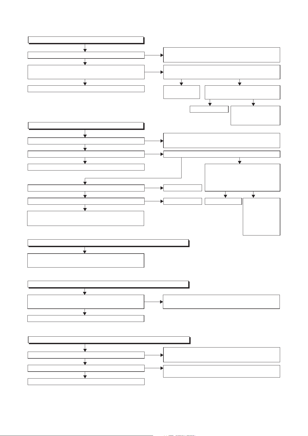
Preparation for Servicing . . . . . . . . . . . . . . . . . . . . . . . . . . . . . . . . . . . . . . . . . . . . . . . . . . . . . . . . . . . . . . . . . 1-6-1
Cabinet Disassembly Instructions . . . . . . . . . . . . . . . . . . . . . . . . . . . . . . . . . . . . . . . . . . . . . . . . . . . . . . . . . . 1-7-1
Electrical Adjustment Instructions . . . . . . . . . . . . . . . . . . . . . . . . . . . . . . . . . . . . . . . . . . . . . . . . . . . . . . . . . . 1-8-1
How to Self-Check and Initialize the HDD & DVD/VCR . . . . . . . . . . . . . . . . . . . . . . . . . . . . . . . . . . . . . . . . . . 1-9-1
Firmware Renewal Mode . . . . . . . . . . . . . . . . . . . . . . . . . . . . . . . . . . . . . . . . . . . . . . . . . . . . . . . . . . . . . . . . 1-10-1
Troubleshooting . . . . . . . . . . . . . . . . . . . . . . . . . . . . . . . . . . . . . . . . . . . . . . . . . . . . . . . . . . . . . . . . . . . . . . . 1-11-1
Function Indicator Symbols . . . . . . . . . . . . . . . . . . . . . . . . . . . . . . . . . . . . . . . . . . . . . . . . . . . . . . . . . . . . . . 1-12-1
Block Diagrams . . . . . . . . . . . . . . . . . . . . . . . . . . . . . . . . . . . . . . . . . . . . . . . . . . . . . . . . . . . . . . . . . . . . . . . 1-13-1
Schematic Diagrams / BOARD’s and Test Points . . . . . . . . . . . . . . . . . . . . . . . . . . . . . . . . . . . . . . . . . . . . . 1-14-1
Waveforms . . . . . . . . . . . . . . . . . . . . . . . . . . . . . . . . . . . . . . . . . . . . . . . . . . . . . . . . . . . . . . . . . . . . . . . . . . . 1-15-1
Wiring Diagram . . . . . . . . . . . . . . . . . . . . . . . . . . . . . . . . . . . . . . . . . . . . . . . . . . . . . . . . . . . . . . . . . . . . . . . 1-16-1
IC Pin Function Descriptions . . . . . . . . . . . . . . . . . . . . . . . . . . . . . . . . . . . . . . . . . . . . . . . . . . . . . . . . . . . . . 1-17-1
Lead Identifications . . . . . . . . . . . . . . . . . . . . . . . . . . . . . . . . . . . . . . . . . . . . . . . . . . . . . . . . . . . . . . . . . . . . 1-18-1
Exploded Views . . . . . . . . . . . . . . . . . . . . . . . . . . . . . . . . . . . . . . . . . . . . . . . . . . . . . . . . . . . . . . . . . . . . . . . 1-19-1
Mechanical Parts List . . . . . . . . . . . . . . . . . . . . . . . . . . . . . . . . . . . . . . . . . . . . . . . . . . . . . . . . . . . . . . . . . . . 1-20-1
Electrical Parts List . . . . . . . . . . . . . . . . . . . . . . . . . . . . . . . . . . . . . . . . . . . . . . . . . . . . . . . . . . . . . . . . . . . . 1-21-1
Manufactured under license from Dolby Laboratories.
“Dolby” and the double-D symbol are trademarks of Dolby Laboratories.
Page 4

SPECIFICATIONS
General
System HDD, DVD-Video, DVD-RW / R, DVD+RW / R, VCD, CD-DA,
VCR video heads Four heads
HDD Internal 3.5 inch HDD 160 GB
Power requirements 220–240 V ± 10%, 50 Hz ± 0.5%
Power consumption 60 W (standby: 8.0 W)
Weight 5.
Dimensions (width x height x depth) 435 x 99.5 x 380 mm
Operating temperature 5°C to 40°C
Operating humidity Less than 80% (no condensation)
TV format P
Recording
Recording format Video Recording format (DVD-RW only),
Recordable discs DVD-ReWritable, DVD-Recordable, DVD+ReWritable,
Video recording format
Sampling frequency
Compression format
Audio recording format
Sampling frequency
Compression format
Tune r
Receivable channels E2-
Input/Output
Front Panel : (AV3)
Video input
Input level
S-Video input
Input level
Audio input
Input level
Rear Panel
VHF/UHF antenna input/output terminal VHF/UHF set 75 Ω
Audio input /output Two 21-pin scart sockets (AV1, AV2)
Video input /output
Input /output level
S-Video output
Output level
Component video out
Output level
Analogue audio output
Output level
Digital audio out
Output level
CD-RW / R, Video Cassette Tape
8 kg (RD-XV47KE/RD-XV47KF)
5.9 kg (RD-XV47KB)
AL / SECAM - BG / DK (RD-XV47KE)
PAL-I (RD-XV47KB)
SECAM LL, PAL B / G (RD-XV47KF)
Video format (DVD-RW, DVD-R)
+VR format (DVD+RW, DVD+R)
DVD+Recordable
13.5 MHz
MPEG2
48 kHz
Dolby Digital
E69 (RD-XV47KE)
IRA-E69 (RD-XV47KB)
"L (SECAM L)": F1 - E69 (RD-XV47KF)
"BG (PAL B / G)": E2 - E69 (RD-XV47KF)
One RCA connector
1 Vp-p (75 Ω)
One Mini DIN 4-pin jack
Y (Iuminance) 1 Vp-p (75 Ω)
C (colour) 300 mVp-p (75 Ω)
Two RCA connectors
2 Vrms (input impedance: more than 10 kΩ)
Two 21-pin scart sockets (AV1, AV2)
1Vp-p (75 Ω) each
One Mini DIN 4-pin jacks
Y (Iuminance) 1 Vp-p (75 Ω)
C (colour) 300 mVp-p (75 Ω)
Three RCA connectors
Y: 1.0 Vp-p (75 Ω)
B/CB
, PR/CR: 0.7 Vp-p (75 Ω) each
P
Two RCA connectors
2 Vrms (output impedance: 680Ω)
One Coaxial pin jack
500 mVp-p (75 Ω)
Note
• The specifications and design of this unit are subject to change without notice.
1-1-1 E3B90SP
Page 5
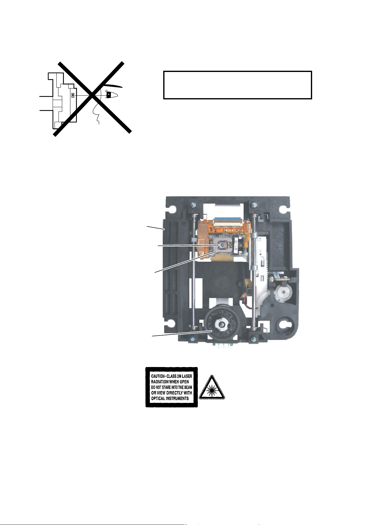
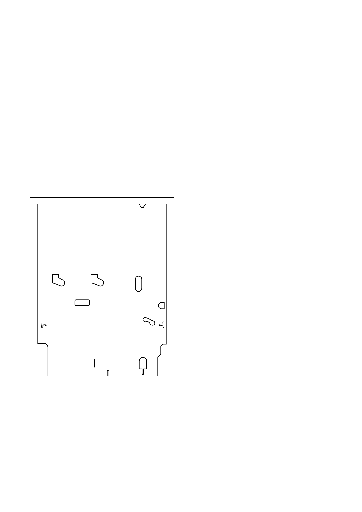
LASER BEAM SAFETY PRECAUTIONS
This DVD player uses a pickup that emits a laser beam.
Do not look directly at the laser beam coming
from the pickup or allow it to strike against your
skin.
The laser beam is emitted from the location shown in the figure. When checking the laser diode, be sure to keep
your eyes at least 30 cm away from the pickup lens when the diode is turned on. Do not look directly at the laser
beam.
CAUTION: Use of controls and adjustments, or doing procedures other than those specified herein, may result in
hazardous radiation exposure.
Drive Mechanism Assembly
Laser Beam Radiation
Laser Pickup
Turntable
Location: Inside Top of DVD mechanism.
1-2-1 R3PLSP
Page 6

IMPORTANT SAFETY PRECAUTIONS
Product Safety Notice
Some electrical and mechanical parts have special
safety-related characteristics which are often not evident from visual inspection, nor can the protection
they give necessarily be obtained by replacing them
with components rated for higher voltage, wattage,
etc. Parts that have special safety characteristics are
identified by a ! on schematics and in parts lists. Use
of a substitute replacement that does not have the
same safety characteristics as the recommended
replacement part might create shock, fire, and/or other
hazards. The Product’s Safety is under review continuously and new instructions are issued whenever
appropriate. Prior to shipment from the factory, our
products are carefully inspected to confirm with the
recognized product safety and electrical codes of the
countries in which they are to be sold. However, in
order to maintain such compliance, it is equally important to implement the following precautions when a set
is being serviced.
Precautions during Servicing
A. Parts identified by the ! symbol are critical for
safety. Replace only with part number specified.
B. In addition to safety, other parts and assemblies
are specified for conformance with regulations
applying to spurious radiation. These must also be
replaced only with specified replacements.
Examples: RF converters, RF cables, noise blocking capacitors, and noise blocking filters, etc.
C. Use specified internal wiring. Note especially:
1)Wires covered with PVC tubing
2)Double insulated wires
3)High voltage leads
D. Use specified insulating materials for hazardous
live parts. Note especially:
1)Insulation tape
2)PVC tubing
3)Spacers
4)Insulators for transistors
E. When replacing AC primary side components
(transformers, power cord, etc.), wrap ends of
wires securely about the terminals before soldering.
F. Observe that the wires do not contact heat produc-
ing parts (heatsinks, oxide metal film resistors, fusible resistors, etc.).
G. Check that replaced wires do not contact sharp
edges or pointed parts.
H. When a power cord has been replaced, check that
5 - 6 kg of force in any direction will not loosen it.
I. Also check areas surrounding repaired locations.
J. Be careful that foreign objects (screws, solder
droplets, etc.) do not remain inside the set.
K. When connecting or disconnecting the internal
connectors, first, disconnect the AC plug from the
AC outlet.
1-3-1 DVD_SFNP
Page 7
Safety Check after Servicing
Examine the area surrounding the repaired location
for damage or deterioration. Observe that screws,
parts, and wires have been returned to their original
positions. Afterwards, do the following tests and confirm the specified values to verify compliance with
safety standards.
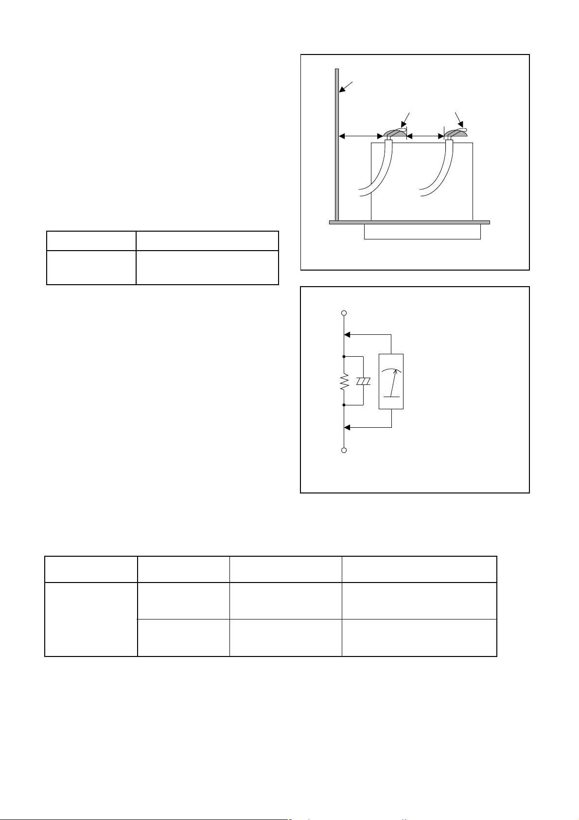
1. Clearance Distance
When replacing primary circuit components, confirm
specified clearance distance (d) and (d’) between soldered terminals, and between terminals and surrounding metallic parts. (See Fig. 1)
Table 1 : Ratings for selected area
AC Line Voltage Clearance Distance (d), (d’)
230 V
Note: This table is unofficial and for reference only.
Be sure to confirm the precise values.
2. Leakage Current Test
≥ 3.2 mm(d)
≥ 6.0 mm(d’)
Chassis or Secondary Conductor
Primary Circuit
d' d
Fig. 1
Exposed Accessible Part
Confirm the specified (or lower) leakage current
between B (earth ground, power cord plug prongs)
and externally exposed accessible parts (RF terminals, antenna terminals, video and audio input and
output terminals, microphone jacks, earphone jacks,
etc.) is lower than or equal to the specified value in the
table below.
Measuring Method (Power ON) :
Insert load Z between B (earth ground, power cord
plug prongs) and exposed accessible parts. Use an
AC voltmeter to measure across the terminals of load
Z. See Fig. 2 and the following table.
Table 2: Leakage current ratings for selected areas
AC Line Voltage Load Z Leakage Current (i)
230 V
2kΩ RES.
Connected in
parallel
50kΩ RES.
Connected in
parallel
i≤0.7mA AC Peak
i≤2mA DC
i≤0.7mA AC Peak
i≤2mA DC
Z
One side of
B
Power Cord Plug Prongs
One side of power cord plug
AC Voltmeter
(High Impedance)
prongs (B) to:
RF or
Antenna terminals
A/V Input, Output
Fig. 2
Note: This table is unofficial and for reference only. Be sure to confirm the precise values.
1-3-2 DVD_SFNP
Page 8
STANDARD NOTES FOR SERVICING
NOTE: BOARD MEANS PRINTED CIRCUIT BOARD.
Circuit Board Indications
1. The output pin of the 3 pin Regulator ICs is
indicated as shown.
Top View
Out
2. For other ICs, pin 1 and every fifth pin are
indicated as shown.
Pin 1
3. The 1st pin of every male connector is indicated as
shown.
Pin 1
Input
In
Bottom View
5
10
Pb (Lead) Free Solder
When soldering, be sure to use the Pb free solder.
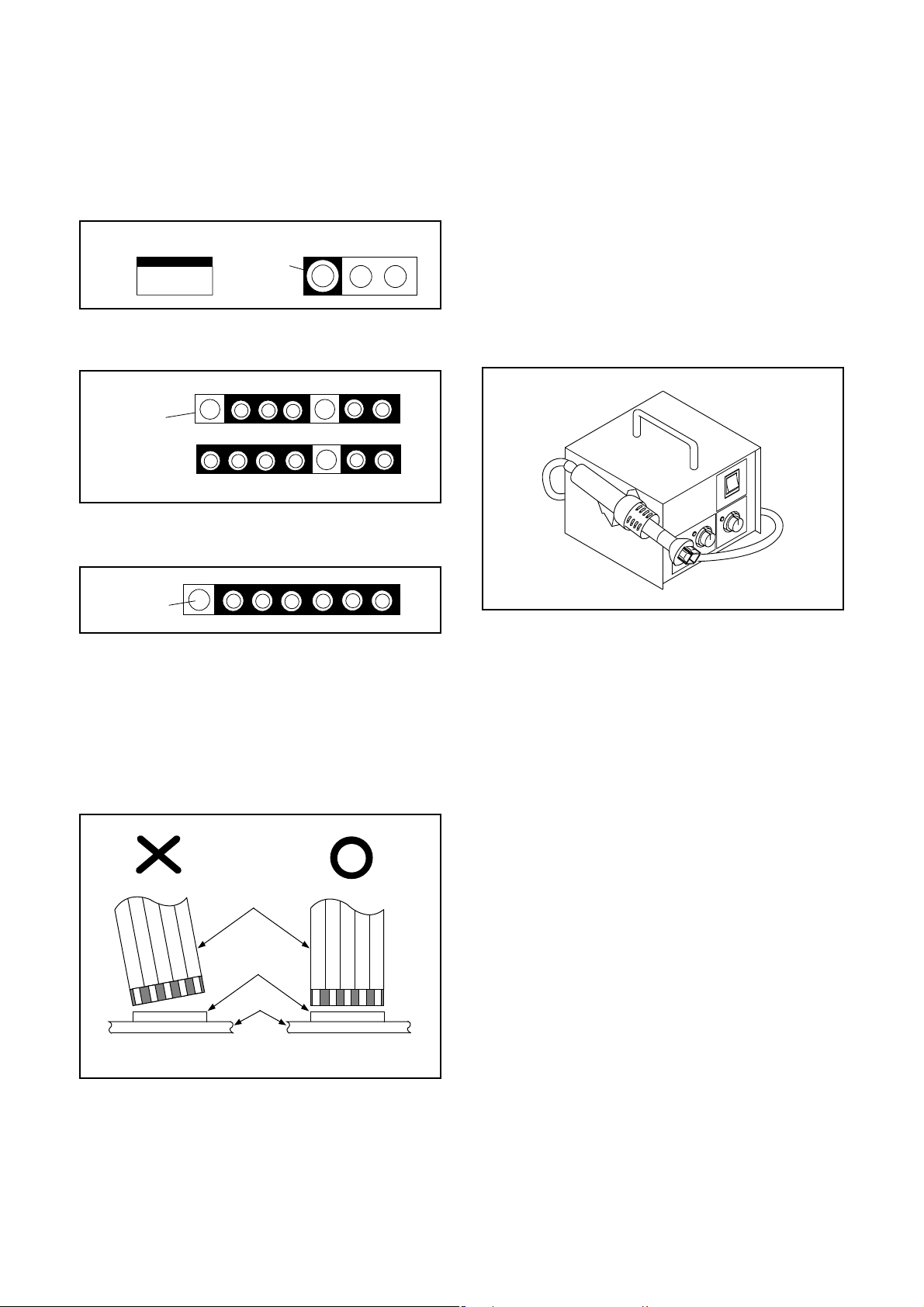
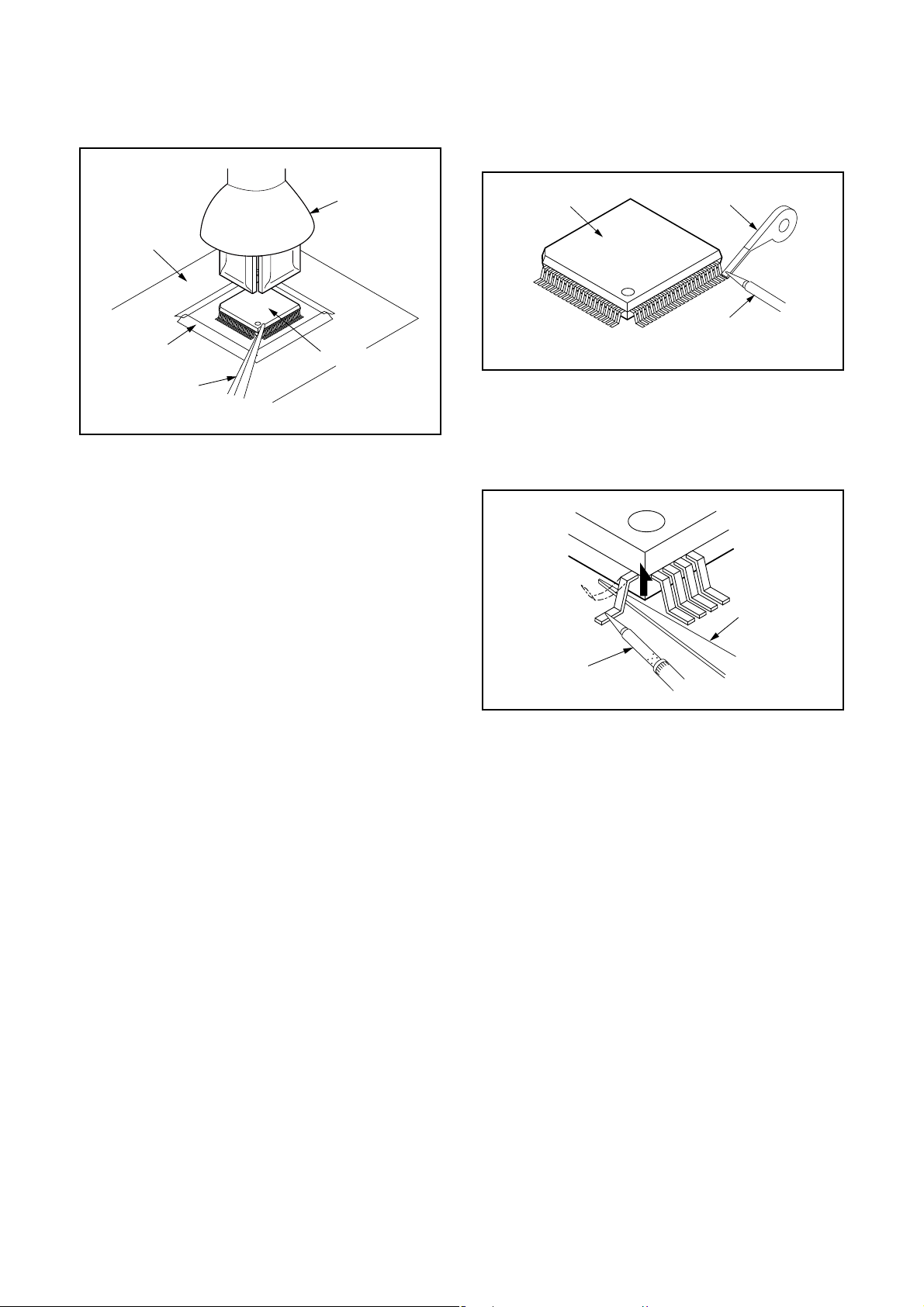
How to Remove / Install Flat Pack-IC
1. Removal
With Hot-Air Flat Pack-IC Desoldering Machine:
1. Prepare the hot-air flat pack-IC desoldering
machine, then apply hot air to the Flat Pack-IC
(about 5 to 6 seconds). (Fig. S-1-1)
Fig. S-1-1
Instructions for Connectors
1. When you connect or disconnect the FFC (Flexible
Foil Connector) cable, be sure to first disconnect
the AC cord.
2. FFC (Flexible Foil Connector) cable should be
inserted parallel into the connector, not at an
angle.
FFC Cable
Connector
BOARD
* Be careful to avoid a short circuit.
2. Remove the flat pack-IC with tweezers while
applying the hot air.
3. Bottom of the flat pack-IC is fixed with glue to the
BOARD; when removing entire flat pack-IC, first
apply soldering iron to center of the flat pack-IC
and heat up. Then remove (glue will be melted).
(Fig. S-1-6)
4. Release the flat pack-IC from the BOARD using
tweezers. (Fig. S-1-6)
CAUTION:
1. The Flat Pack-IC shape may differ by models. Use
an appropriate hot-air flat pack-IC desoldering
machine, whose shape matches that of the Flat
Pack-IC.
2. Do not supply hot air to the chip parts around the
flat pack-IC for over 6 seconds because damage
to the chip parts may occur. Put masking tape
around the flat pack-IC to protect other parts from
damage. (Fig. S-1-2)
1-4-1 DVDN_SN
Page 9
3. The flat pack-IC on the BOARD is affixed with
glue, so be careful not to break or damage the foil
of each pin or the solder lands under the IC when
removing it.
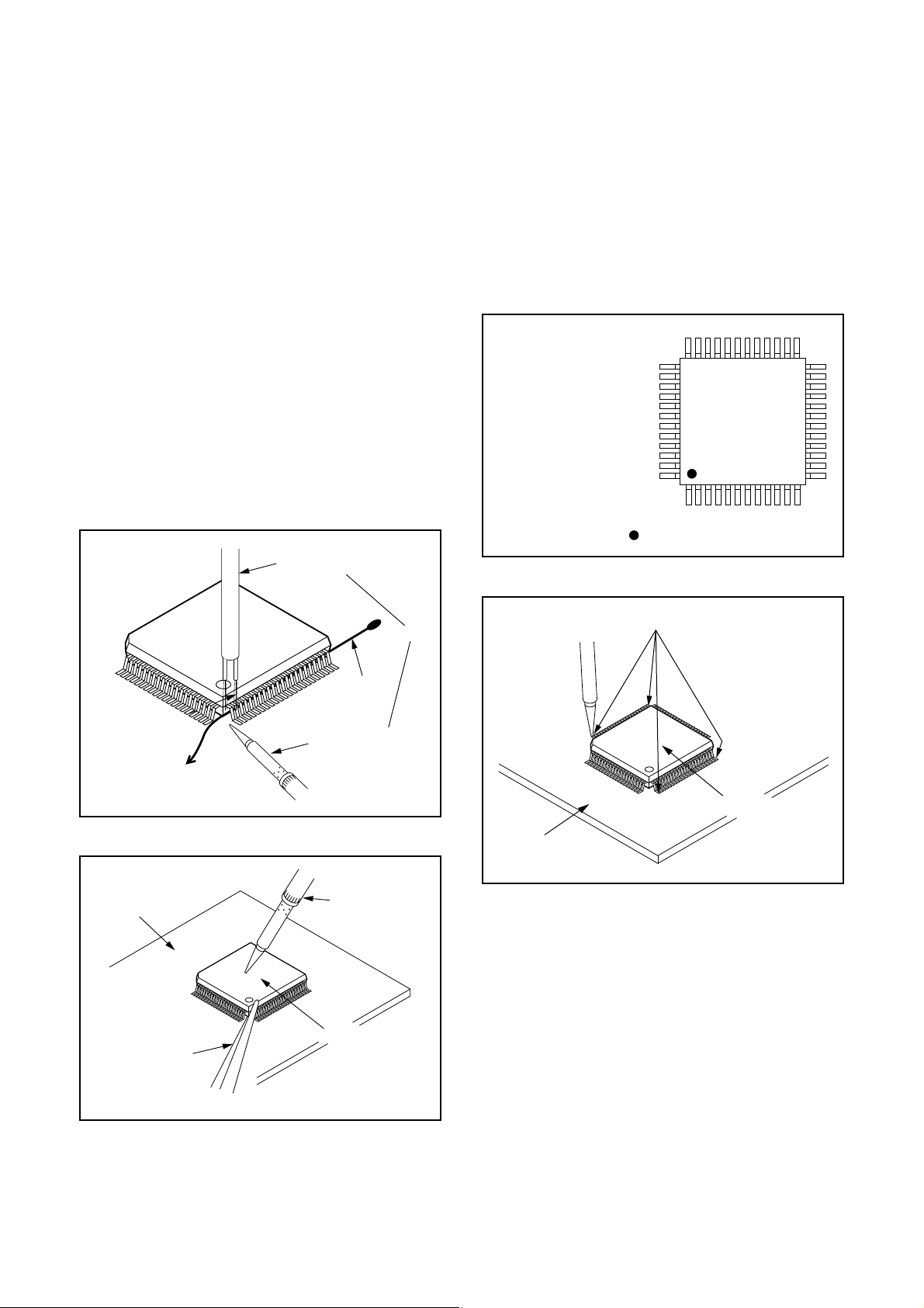
With Soldering Iron:
1. Using desoldering braid, remove the solder from
all pins of the flat pack-IC. When you use solder
flux which is applied to all pins of the flat pack-IC,
you can remove it easily. (Fig. S-1-3)
BOARD
Masking
Tape
Tweezers
Hot-air
Flat Pack-IC
Desoldering
Machine
Flat Pack-IC
Fig. S-1-2
Flat Pack-IC
Desoldering Braid
Soldering Iron
Fig. S-1-3
2. Lift each lead of the flat pack-IC upward one by
one, using a sharp pin or wire to which solder will
not adhere (iron wire). When heating the pins, use
a fine tip soldering iron or a hot air desoldering
machine. (Fig. S-1-4)
Sharp
Pin
Fine Tip
Soldering Iron
3. Bottom of the flat pack-IC is fixed with glue to the
BOARD; when removing entire flat pack-IC, first
apply soldering iron to center of the flat pack-IC
and heat up. Then remove (glue will be melted).
(Fig. S-1-6)
4. Release the flat pack-IC from the BOARD using
tweezers. (Fig. S-1-6)
Fig. S-1-4
1-4-2 DVDN_SN
Page 10
With Iron Wire:
1. Using desoldering braid, remove the solder from
all pins of the flat pack-IC. When you use solder
flux which is applied to all pins of the flat pack-IC,
you can remove it easily. (Fig. S-1-3)
2. Affix the wire to a workbench or solid mounting
point, as shown in Fig. S-1-5.
3. While heating the pins using a fine tip soldering
iron or hot air blower, pull up the wire as the solder
melts so as to lift the IC leads from the BOARD
contact pads as shown in Fig. S-1-5.
4. Bottom of the flat pack-IC is fixed with glue to the
BOARD; when removing entire flat pack-IC, first
apply soldering iron to center of the flat pack-IC
and heat up. Then remove (glue will be melted).
(Fig. S-1-6)
5. Release the flat pack-IC from the BOARD using
tweezers. (Fig. S-1-6)
Note: When using a soldering iron, care must be
taken to ensure that the flat pack-IC is not
being held by glue. When the flat pack-IC is
removed from the BOARD, handle it gently
because it may be damaged if force is applied.
Hot Air Blower
2. Installation
1. Using desoldering braid, remove the solder from
the foil of each pin of the flat pack-IC on the
BOARD so you can install a replacement flat packIC more easily.
2. The “●” mark on the flat pack-IC indicates pin 1.
(See Fig. S-1-7.) Be sure this mark matches the 1
on the BOARD when positioning for installation.
Then presolder the four corners of the flat pack-IC.
(See Fig. S-1-8.)
3. Solder all pins of the flat pack-IC. Be sure that
none of the pins have solder bridges.
Example :
Pin 1 of the Flat Pack-IC
is indicated by a " " mark.
Fig. S-1-7
To Solid
Mounting Point
BOARD
Tweezers
Iron Wire
Soldering Iron
Fig. S-1-5
Fine Tip
Soldering Iron
Flat Pack-IC
or
Presolder
Flat Pack-IC
BOARD
Fig. S-1-8
Fig. S-1-6
1-4-3 DVDN_SN
Page 11
Instructions for Handling Semiconductors
Electrostatic breakdown of the semi-conductors may
occur due to a potential difference caused by
electrostatic charge during unpacking or repair work.
1. Ground for Human Body
Be sure to wear a grounding band (1 MΩ) that is
properly grounded to remove any static electricity that
may be charged on the body.
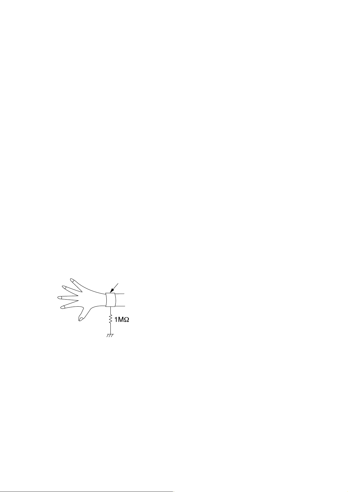
2. Ground for Workbench
Be sure to place a conductive sheet or copper plate
with proper grounding (1 MΩ) on the workbench or
other surface, where the semi-conductors are to be
placed. Because the static electricity charge on
clothing will not escape through the body grounding
band, be careful to avoid contacting semi-conductors
with your clothing.
<Incorrect>
<Correct>
1MΩ
BOARD
Grounding Band
1MΩ
BOARD
Conductive Sheet or
Copper Plate
1-4-4 DVDN_SN
Page 12
HANDLING PRECAUTIONS FOR HDD
CAUTION:
1. SHOCK
a. Exposing HDD to shock may be the biggest
damaging factor. Please note that HDD is easily
damaged even if dropped from any height. Be sure
to place HDD on a shock-absorbent mat. Also, be
careful when transporting HDD.
b. Be careful not to subject HDD to any shock when
tightening screws for HDD replacement.
(Tighten screws manually, not with an electric
driver.)
2. MOISTURE
a. Moisture may also be a damaging factor. HDD is
semiclosed style. Sudden changes in ambient
temperature may cause moisture to form. Monitor
temperature and do not allow moisture to form on
the media surface. Also, when opening HDD
package, do so only after package is at ambient
temperature.
b. After replacing HDD, leave it to reach room
temperature (about 2 hours) for preventing dew
internal condensation, and then work necessary
task such as operation check.
4. OTHERS
a. Be careful so as not to do the followings.
Otherwise, HDD might be damaged.
- DO NOT disassemble HDD.
- When handling HDD, be sure to hold both sides
securely.
b. HDD should be stored, packed in the protective
bag, in suitable surroundings (i.e., no extreme
changes in temperature to avoid condensation).
c. When transporting HDD, be sure to use the
exclusive packing case (the replacement HDD
carton).
d. Do not stack HDDs.
e. Do not place vertically because HDD is unstable
and easy to fall.
3. STATIC ELECTRICITY
a. After removing HDD or taking replacement HDD
out of the protective bag (the replacement HDD is
packed in a protective bag), place HDD on a
conductive surface. A grounding band should be
worn when handling.
Grounding Band
Both the conductive surface and grounding band
should be grounded.
b. Make sure that HDD is placed on main unit
completely and then let go of it, when assembling.
c. Do not put HDD on a packing bag. (for preventing
electrostatic damage)
1-5-1 DHD_SN
Page 13
PREPARATION FOR SERVICING
How to Enter the Service Mode
About Optical Sensors
Caution:
An optical sensor system is used for the Tape Start
and End Sensors on this equipment. Carefully read
and follow the instructions below. Otherwise the unit
may operate erratically.
What to do for preparation
Insert a tape into the Deck Mechanism Assembly and
press [VCR PLAY] button. The tape will be loaded into
the Deck Mechanism Assembly. Make sure the power
is on, connect J78 to GND. This will stop the function
of Tape Start Sensor, Tape End Sensor and Reel Sensors. (If these TPs are connected before plugging in
the unit, the function of the sensors will stay valid.)
See Fig. 1.
Q503
J78
Note: Because the Tape End Sensors are inactive, do
not run a tape all the way to the start or the end of the
tape to avoid tape damage.
Q504
Fig. 1
1-6-1 E3B90PFS
Page 14
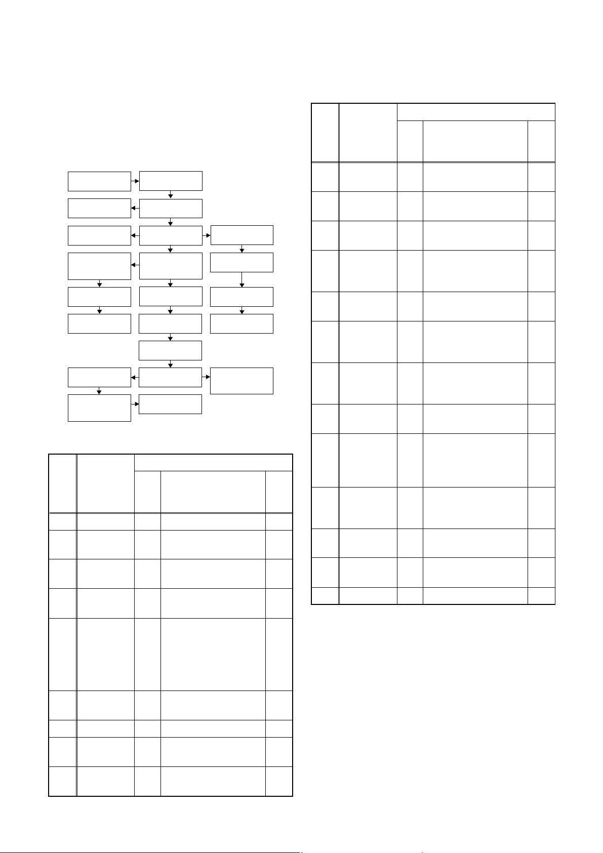
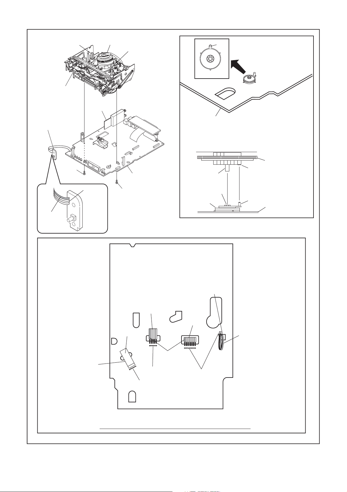
CABINET DISASSEMBLY INSTRUCTIONS
NOTE: BOARD MEANS PRINTED CIRCUIT BOARD.
1. Disassembly Flowchart
This flowchart indicates the disassembly steps to gain
access to item(s) to be serviced. When reassembling,
follow the steps in reverse order. Bend, route, and
dress the cables as they were originally.
[1] Cover Top
[21] Front
Bracket R
[22] Bracket R
[13] BOARD
POWER
SUPPLY
[14] BOARD
SWITCH
[15] BOARD
FRONT JACK
[17] Deck
Assembly
[18] BOARD
POWER,
BOARD AFV
[2] Front
Assembly
[3] Front
Bracket
[4] HDD
Assembly
[5] DVD Mechanism
& DVD/HDD MAIN
BOARD Assembly
[10] Fan Holder
[11] Brushless
Cooling Fan
[12] Panel Rear
[16] VCR
Chassis Unit
[20] Deck
Pedestal
[6] HDD
Bracket
[7] HDD Unit
[8] HDD
Support
[9] BOARD ATA
[19] BOARD
POWER
SWITCH
2. Disassembly Method
ID/
LOC.
No.
PART
Fig.
No.
[1] Cover Top D1 7(S-1) ---
Front
[2]
[3]
[4]
Assembly
Front
Bracket
HDD
Assembly
D2 (S-2), *5(L-1), *3(L-2) 1
D2
D3
DVD
Mechanism
[5]
& DVD/
HDD MAIN
D3
BOARD
Assembly
HDD
[6]
Bracket
D4
[7] HDD Unit D4 4(S-8), HDD Rubber 2
HDD
[8]
[9]
Support
BOARD
ATA
D4 Insulation Sheet ---
D4 *CN3001, *CN3002 ---
REMOVAL
REMOVE/*UNHOOK/
UNLOCK/RELEASE/
UNPLUG/DESOLDER
2(S-3), 3(S-3B), Front
Support
2(S-4), *CN901,
*CN1003
2(S-5), 2(S-6),
*CN1001, *CN1502,
Cover Dust
4(S-7), (S-7B), Plate
Earth
Note
---
---
2
---
ID/
LOC.
PART
No.
[10] Fan Holder D5
Brushless
[11]
Cooling
Fan
[12] Panel Rear D5
REMOVE/*UNHOOK/
Fig.
UNLOCK/RELEASE/
No.
UNPLUG/DESOLDER
Note
3(S-9), 2(S-9B),
*CN1002
D5 ---------- ---
3(S-10), 2(S-10B),
2(S-11)
---
---
BOARD
REMOVAL
[13]
POWER
D6 *CL1001, 4(S-12) ---
SUPPLY
BOARD
[14]
SWITCH
D6 (S-13), Desolder ---
BOARD
[15]
FRONT
D6 *CN3001, 2(S-14) ---
JACK
[16]
[17]
VCR
Chassis
Unit
Deck
Assembly
5(S-15), 4(S-16),
D7
(S-17)
(S-18), (S-19)
D8
Desolder
---
BOARD
POWER,
[18]
BOARD
D8 ---------- ---
AFV
BOARD
[19]
POWER
D8 Desolder ---
SWITCH
Deck
[20]
[21]
Pedestal
Front
Bracket R
D9 8(S-20) ---
D9 (S-21) ---
[22] Bracket R D9 2(S-22) ---
↓
(1)
↓
(2)
↓
(3)
↓
(4)
(5)
Note:
(1): Identification (location) No. of parts in the figures
(2): Name of the part
(3): Figure Number for reference
(4): Identification of parts to be removed, unhooked,
unlocked, released, unplugged, unclamped, or
desoldered.
P=Spring, L=Locking Tab, S=Screw,
CN=Connector
*=Unhook, Unlock, Release, Unplug, or Desolder
e.g. 6(S-1) = six Screws (S-1),
5(L-1) = five Locking Tabs (L-1)
(5): Refer to “Reference Notes.”
3
4
↓
1-7-1 E3B90DC
Page 15
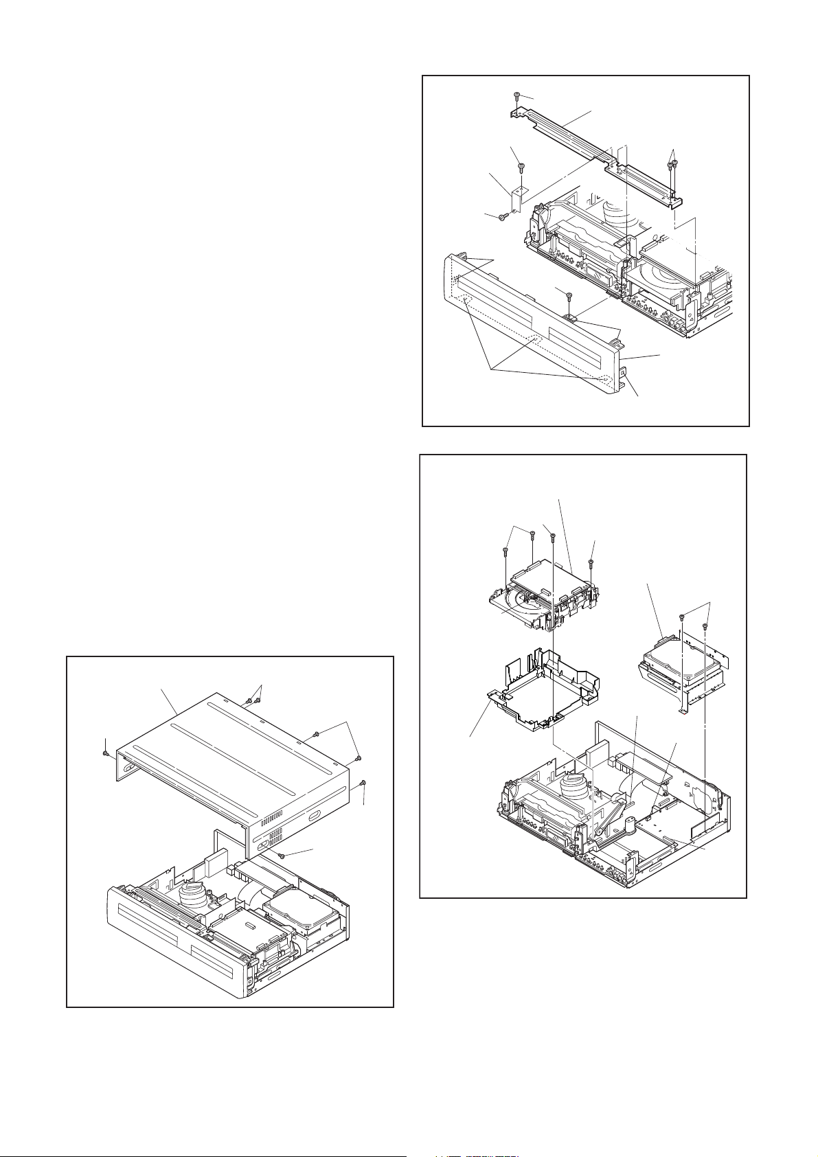
Reference Notes
1. Locking Tabs (L-1) and (L-2) are fragile. Be careful
not to break them.
1-1. Remove Screw (S-2).
1-2. Release five Locking Tabs (L-1).
1-3. Release three Locking Tabs (L-2) and
remove the Front Assembly.
2. Do not replace the DVD Mechanism or the DVD/
HDD MAIN BOARD Assembly separately, when
replacing the DVD Mechanism & DVD/HDD MAIN
BOARD Assembly. Order the new DVD
Mechanism & DVD/HDD MAIN BOARD Assembly.
2-1. Whenever you have replaced the HDD unit,
initialize the HDD unit. To initialize the HDD
unit, perform the following.To put the HDD &
DVD/VCR into the HDD mode, press the
[HDD] button on the remote control unit.
2-2. To put the HDD & DVD/VCR into the self-
check mode, after pressing [VARIABLE
SKIP] button, press the [3], [6], and [9]
buttons on the remote control in that order
within three seconds.
2-3. Press [ENTER] button. The HDD & DVD/
VCR is initialized and the power is turned off
automatically after two seconds.
3. When reassembling, solder wire jumpers as
shown in Fig. D8.
4. Before installing the Deck Assembly, be sure to
place the pin of LD-SW on the BOARD POWER
as shown in Fig. D8. Then, install the Deck
Assembly while aligning the hole of Cam Gear
with the pin of LD-SW, the shaft of Cam Gear with
the hole of LD-SW as shown in Fig. D8.
(S-3B)
(S-3B)
Front
Support
(S-3B)
(L-1)
(S-2)
(L-2)
[5] DVD Mechanism &
DVD/HDD MAIN BOARD
Assembly
(S-6)
(S-5)
CN901
[3] Front Bracket
(S-3)
(L-1)
[2] Front
Assembly
(L-1)
Fig. D2
(S-5)
[4] HDD Assembly
(S-4)
[1] Cover Top
(S-1)
(S-1)
(S-1)
(S-1)
(S-1)
Fig. D1
Cover Dust
CN1502
CN1003
CN1001
Fig. D3
1-7-2 E3B90DC
Page 16
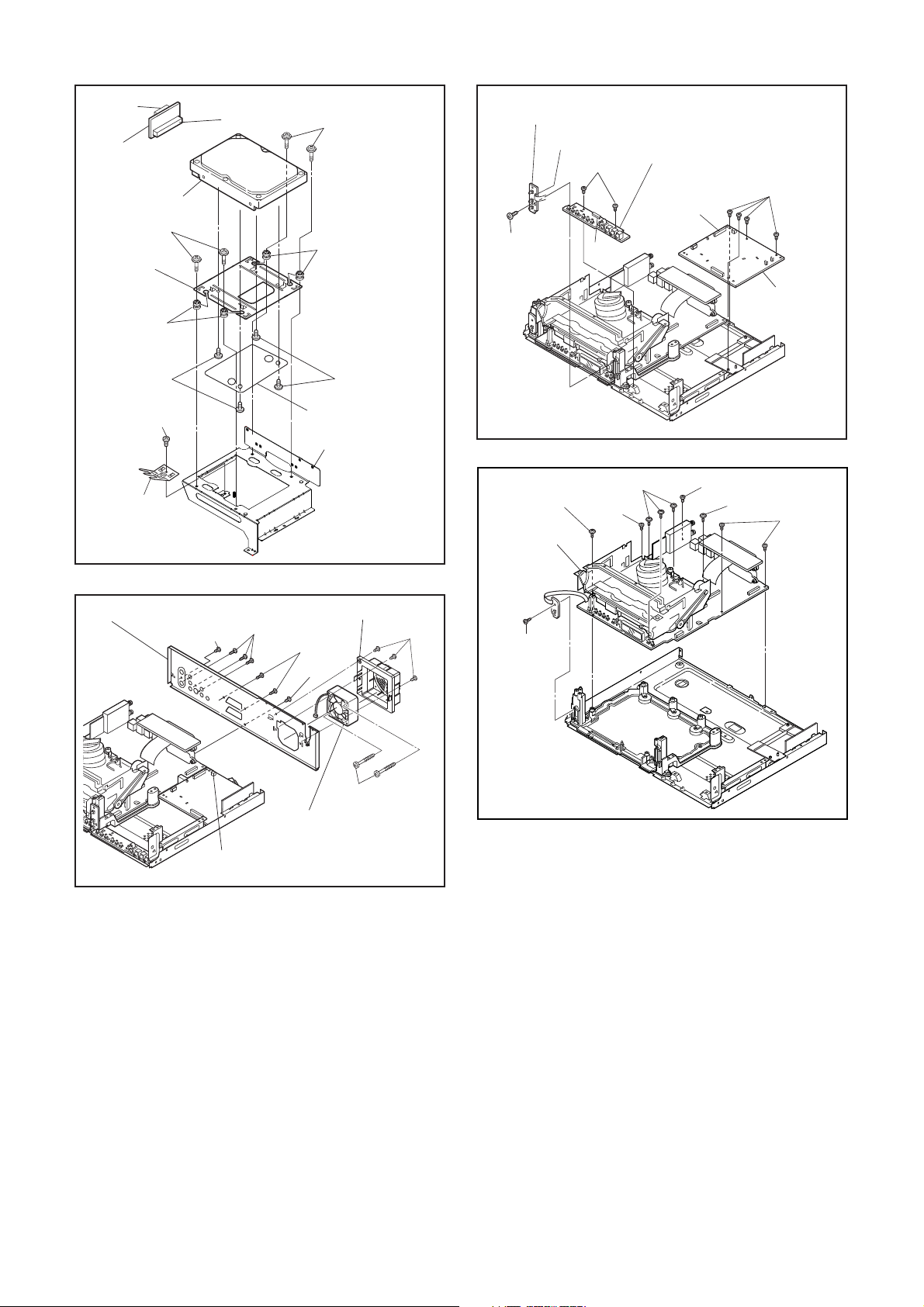
CN3002
[9] BOARD ATA
[7] HDD Unit
(S-7)
[8] HDD
Support
HDD Rubber
CN3001
(S-7)
HDD Rubber
[14] BOARD SWITCH
Desolder
(S-14)
(S-13)
CN3001
[15] BOARD FRONT JACK
(S-12)
CL1001
[13] BOARD
POWER
SUPPLY
(S-8)
(S-7B)
Plate Earth
[12] Panel Rear
(S-11)
(S-10)
CN1002
(S-8)
Insulation Sheet
[6] HDD Bracket
[10] Fan Holder
(S-10B)
(S-11)
(S-9B)
[11] Brushless
Cooling Fan
Fig. D4
(S-9)
Fig. D5
(S-15)
[16] VCR
Chassis
Unit
(S-17)
(S-15)
(S-16)
Fig. D6
(S-16)
(S-15)
(S-16)
Fig. D7
1-7-3 E3B90DC
Page 17
FE Head
[17] Deck
Assembly
[19] BOARD
POWER SWITCH
(S-18)
[18]
BOARD
AFV
Cylinder
Assembly
ACE Head
Assembly
[18] BOARD POWER
Pin
Pin
SW507
LD-SW
[18] BOARD POWER
[17] Deck Assembly
Cam Gear
Hole
Shaft
Lead with
blue stripe
Desolder
From
Capstan
Motor
Assembly
(S-19)
Printing side
From
ACE Head
Assembly
Desolder
Desolder
Lead with
blue stripe
LD-SW
From
Cylinder
Assembly
Desolder
Hole
Pin
[18] BOARD
POWER
From
FE Head
Lead with
gray stripe
BOTTOM VIEW
Lead connections of Deck Assembly and BOARD POWER
1-7-4 E3B90DC
Fig. D8
Page 18
(S-20)
(S-20)
[20] Deck Pedestal
[21] Front Bracket R
[22] Bracket R
(S-22)
(S-21)
Fig. D9
3. How to Eject Manually
Note: When rotating the gear, be careful not to damage the gear.
1. Remove the Cover Top.
2. Rotate the gear in the direction of the arrow manually as shown below.
Rotate this gear in
the direction of the arrow
A
View for A
1-7-5 E3B90DC
Page 19
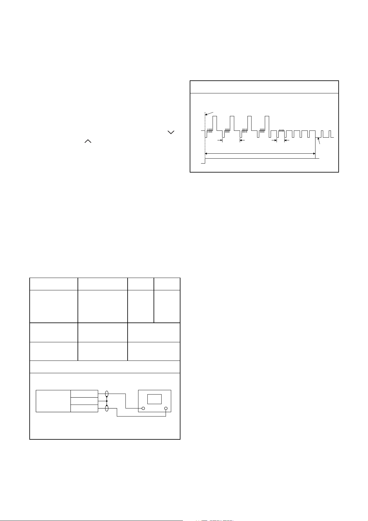
ELECTRICAL ADJUSTMENT INSTRUCTIONS
NOTE: BOARD MEANS PRINTED CIRCUIT BOARD.
NOTE:
1.Electrical adjustments are required after replacing
circuit components and certain mechanical parts.
It is important to do these adjustments only after
all repairs and replacements have been completed. Also, do not attempt these adjustments
unless the proper equipment is available.
2.To perform these alignment / confirmation procedures, make sure that the tracking control is set in
the center position: Press either [PROGRAM 5??]
or [PROGRAM ] button on the front panel first,
then the [ O ] (VCR) button on the front panel.
CH1
CH2
Figure 1
EXT. Syncronize Trigger Point
1.0H
6.5H±1H (416 μs ± 64 μs)
0.5H
V-Sync
Test Equipment Required
1.Oscilloscope: Dual-trace with 10:1 probe,
V-Range: 0.001~50V/Div.,
F-Range: DC~AC-20MHz
2.Alignment Tape (FL6A)
Head Switching Position Adjustment
Purpose:
To determine the Head Switching position during
playback.
Symptom of Misadjustment:
May cause Head Switching noise or vertical jitter
in the picture.
Test point Adj.Point Mode Input
J308(
AV1-V- OUT
TP504(RF-SW)
GND
Tape
)
VR501
(Switching Point)
(BOARD
POWER)
Measurement
Equipment
PLAY
(SP)
-----
Spec.
Switching Pulse
Reference Notes:
Playback the Alignment tape and adjust VR501 so that
the V-sync front edge of the CH1 video output waveform is at the 6.5H±1H (416μs±64μs) delayed position
from the rising edge of the CH2 head switching pulse
waveform.
FL6A Oscilloscope
Connections of Measurement Equipment
BOARD
POWER
J308
GND
TP504
6.5H±1H
(416μs±64μs)
Oscilloscope
CH1 CH2
Trig. (+)
1-8-1 E3B90EA
Page 20
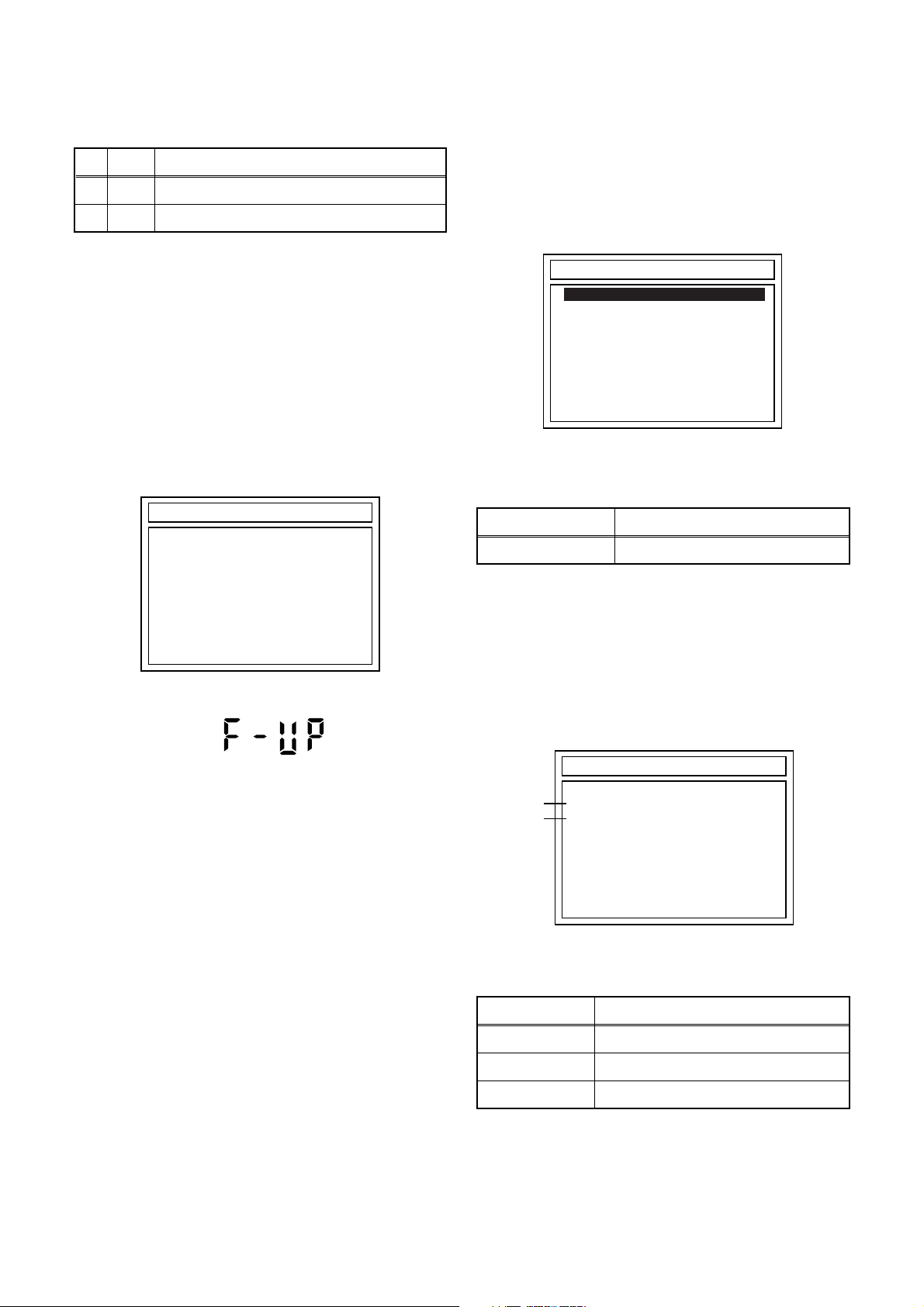
HOW TO SELF-CHECK AND INITIALIZE THE HDD & DVD/VCR
1. Turn on the HDD & DVD/VCR.
2. To put the HDD & DVD/VCR into the HDD mode, press [HDD] on the remote control unit.
3. To put the HDD & DVD/VCR into the self-check mode, after pressing [VARIABLE SKIP] button, press the [3],
[6], and [9] buttons on the remote control in that order within three seconds.
Fig. a appears on the screen and all LEDs light.
"
" differs depending on the models.
*******
Self-Analysys and Report
*1
*2
*3
DVD CONNECT STATUS :
HDD CONNECT STATUS :
HDD POWER ON HOURS :
*4
*5
*6
BE Ver. :
FE Ver. :
Sub Micon Ver. :
T3*****B2S-****
R35_028_000
T3***TTP
Fig. a: Self-Check Mode Screen
Table 1: Description of Fig. a
INDICATION DESCRIPTION
DVD CONNECT STATUS (*1) Connecting Condition of DVD(F/E)
HDD CONNECT STATUS (*2) Connecting Condition of HDD
Value of HDD power on hours obtained from S.M.A.R.T. command. (If not obtainable,
HDD POWER ON HOURS (*3)
value of HDD power on hours is “0”.)
Value in parentheses is the factory setting value. (If no setting, the value is “0”.)
BE Ver. (*4) B/E version
FE Ver. (*5) F/E version
Sub Micon Ver. (*6) Sub micro controller version
4. Upon the self-check completion, Fig. b appears on the screen.
"
" differs depending on the models.
*******
Self-Analysys and Report
*7
*8
DVD CONNECT STATUS : OK
HDD CONNECT STATUS : OK
HDD POWER ON HOURS : 100(40)
*10
BE Ver. :
FE Ver. :
Sub Micon Ver. :
*9
FACTORY DEFAULT :
POWER OFF :
T3*****B2S-****
R35_028_000
T3***TTP
ENTER
POWER
Fig. b: Screen of Finishing Self-Check Mode
1-9-1 E3B90INT
Page 21
Table 2: Indication of DVD self-check (*7)
INDICATION DESCRIPTION
OK Connection of DVD is normal.
NOT FOUND DVD drive cannot be found.
CABLE ERROR
FFC cable (connecting to CN401) between the DVD drive and the DVD/HDD MAIN BOARD
is not connected correctly.
Table 3: Indication of HDD self-check (*8)
INDICATION DESCRIPTION
OK Connection of HDD is normal.
NOT FOUND HDD drive cannot be found.
CABLE ERROR FFC cable between the BOARD ATA and the HDD drive is not connected correctly.
Table 4: Available button in self-check mode
BUTTON DESCRIPTION
ENTER (*9) Initialize (only when the self-check mode is complete)
ON / STANDBY (*10) Turn the power off (when the self-check mode is complete)
OTHER Not available
5. When the self-check mode is complete, press [ ] button to turn the power off.
When initializing the HDD & DVD/VCR, press [ENTER] button. Fig. c appears on the screen. After two
seconds, the power is turned off automatically.
"
" differs depending on the models.
*******
SELF CHECK
DVD CONNECT STATUS : OK
HDD CONNECT STATUS : OK
HDD POWER ON HOURS : 100(40)
BE Ver. :
FE Ver. :
Sub Micon Ver. :
HDD FORMAT : *11WRITING
T3*****B2S-****
R35_028_000
T3***TTP
Fig. c: Initialize Mode Screen
Table 5: Description of *11 in Fig. c
INDICATION DESCRIPTION
ENTER Initialization preparation is complete.
WRITING Initializing
OK Initializing is finished normally.
NG Initializing is not finished normally.
NOTE: When initializing, “Current Clock”, “Setup Changing Item”, “Channel Setup”, “Area Setup”, “Program” and
“HDD Contents” are initialized.
1-9-2 E3B90INT
Page 22
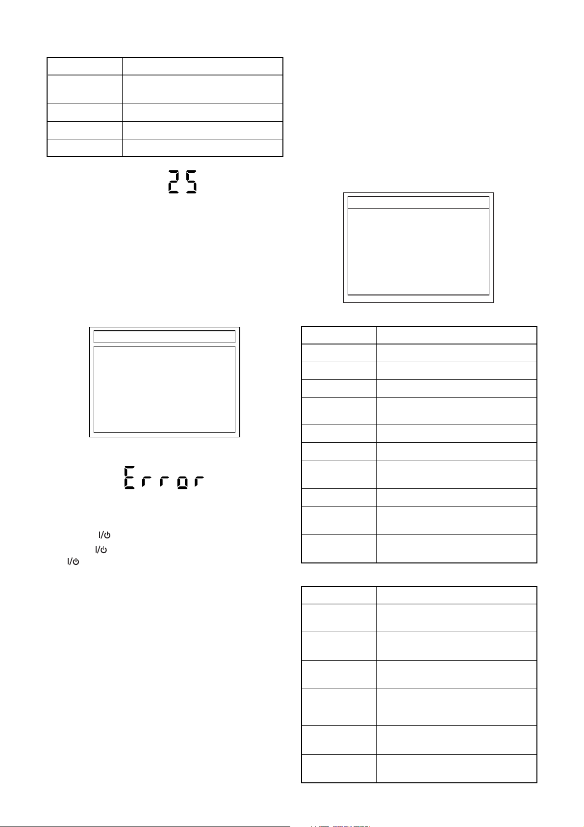
FIRMWARE RENEWAL MODE
1. Update Contents
Item Status
1 B/E Update B/E FIRMWARE
2 F/E Update F/E FIRMWARE
2. Update
1. Turn the power on and remove the disc in the tray.
2. To switch the HDD & DVD into the HDD mode,
press [HDD] on the remote control unit.
3. To put the HDD & DVD into version up mode,
press [VARIABLE SKIP] and [6], [5], [4] buttons on
the remote control unit in that order within 3
seconds. The tray will open automatically.
Fig. a appears on the TV screen and Fig. b
appears on the VFD.
*FIRMWARE version will differ depending on the
model. Fig. a is an example.
DISC UPDATE
4. Load the update disc.
The TV screen will display Fig. c.
- If the update disc contains only a single file, the
update will initiate automatically when the disc is
inserted.
*FIRMWARE version will differ depending on the
model. Fig. c is an example.
DISC UPDATE
T3T00361B2S.MOT
<DIR> BE
<DIR> FE
Fig. c: Update Disc TV Screen
Effective FIRMWARE update files will have the file
extensions shown below.
File extension Status
MOT F/E FIRMWARE file
Please Insert F/W Disc
Fig. a: Update Mode TV Screen
Fig. b: VFD Display in Update Mode
5. Select the desired FIRMWARE to be updated with
the arrow button and press the [ENTER] or [PLAY]
button.
The tray will open automatically; close the tray by
pressing [OPEN/CLOSE] button or by hand.
6. Fig. d appears on the TV screen and Fig. e
appears on the VFD, and the update will start.
*FIRMWARE version will differ depending on the
model. Fig. d is an example.
DISC UPDATE
*1
TARGET: B/E
*2
STATUS: EXECUTING
DISC UPDATING
Fig. d: TV Display during update
The status displayed in *1 is as shown below.
Display Status
B/E FIRMWARE B/E
F/E FIRMWARE F/E
UNKNOWN Not FIRMWARE B/E or F/E
1-10-1 E3B90FW
Page 23
The status displayed in *2 is as shown below.
Display Status
EXECUTING
Loading F/W from Update Disc or
writing to Flash memory
ERROR Error during Flash memory writing
FILE ERROR Check SAM error in F/W file
READ ERROR Error during F/W file reading
3. How to Verify the Firmware
Version
1. Turn the power on and remove the disc in the tray.
2. To switch the HDD & DVD into HDD mode, press
[HDD] on the remote control unit.
3. To put the HDD & DVD into version display mode,
press [VARIABLE SKIP] and [1], [2], [3] buttons on
the remote control unit in that order within 3
seconds. Fig. i appears on the TV screen.
******* part will differ depending on the model.
Fig. i is an example.
Fig. e: VFD Display during update
When the TV screen displays "Firmware
Updating... XX% Complete," the VFD will indicate
"XX"%.
7. When update is complete, the unit will shut off
automatically.
8. If an error occured during updating, the TV screen
will display Fig. f.
*FIRMWARE version will differ depending on the
model. Fig. f is an example.
DISC UPDATE
TARGET: B/E
STATUS: ERROR
PLEASE PUSH POWER BUTTON
Fig. f: TV Display when completing update with error
VERSION INFORMATION
Model Name :
BE Ver. :
FE Ver :
Sub Micon Ver. :
REGION:
CPRM KEY NO:
HDD MODEL:
DivX Ver.:
LD ADJUSTMENT:
DISC ADJUSTMENT:
E3B90ED
T3*****B2S-****
R35_***_***
T3***TTP
2
(0x***)
***********(***GByte)
***
OK
OK
Fig. i: Firmware version display
Display Contents
MODEL NAME Product number
BE Ver. Firmware B/E version
FE Ver. Application F/E version
Sub Micon Ver.
Sub Microcontroller firmware
version
REGION Region code of playable DVD disc
CPRM KEY NO.
HDD MODEL
CPRM key number
HDD serial number and capacity
(GByte)
Fig. h: VFD Display when completing update with error
In this case, all button operations will be invalid
except [ ] button.
9. Press [ ] button to turn the power off and press
[ ] button again to turn the power back on and
finish updating.
DivX Ver. Version number of DivX filesystems
LD
ADJUSTMENT
DISC
ADJUSTMENT
LD adjustment progress (done: OK/
not done: --)
Factory adjustment progress (done:
OK/not done: --)
Effective buttons in this mode are the following...
Buttons Operations
POWER
SETUP
TOP MENU
Power off to release from this
mode.
Version display disappears and
SETUP screen appears.
Version display disappears and
TOP MENU screen appears.
Version display disappears and
TIMER PROG.
TIMER PROGRAMMING screen
appears.
DUBBING
MENU
Others
Version display disappears and
DUBBING screen appears.
While displaying version and
normal operation.
1-10-2 E3B90FW
Page 24
NOTE: BOARD MEANS PRINTED CIRCUIT BOARD.
1 Power Supply Section
FLOW CHART NO.1
The power cannot be turned on.
TROUBLESHOOTING
Is the fuse normal?
Ye s
Is normal state restored when once unplugged
power cord is plugged again after several seconds.
Ye s
Is the AL+5V line voltage normal?
Ye s
Check each rectifying circuit of secondary circuit
and service it if defective.
FLOW CHART NO.2
The fuse blows out.
Check the presence that the primary component
is leaking or shorted and service it if defective.
After servicing, replace the fuse.
FLOW CHART NO.3
When the output voltage fluctuates.
No
No
No
See FLOW CHART No.2 <The fuse blows out.>
Check for lead or short-circuiting of primary
circuit component and service it if defective.
(Q1001, Q1003, T1001, D1001, D1002, D1003,
D1004, R1003)
Check the presence that the rectifying diode or circuit
is shorted in each rectifying circuit of secondary side
and service it if defective.
Does the secondary side photo coupler circuit
operate normally?
Ye s
Check the circuit and service it if defective.
(IC1001, D1025, D1022, D1023)
FLOW CHART NO.4
When buzz sound can be heard in the vicinity of power circuit.
Check if there is short circuit on the rectifying diode and the circuit in each rectifying circuit of secondary side
and service it if defective. (D013, D014, D016, D018, D019, D1030, D1031, D1032, D1035, D1101, IC1103,
IC1104, IC1105, Q1100, Q1102, Q1105, Q1106, Q1108, Q1114, Q1502, Q1508, Q1511, Q1513, Q1516,
Q1517, Q1518, Q1519, Q1520, Q1521)
FLOW CHART NO.5
-FL is not outputted.
Is the supply voltage of -24V fed to the anode of
D012?
Ye s
Check for load circuit short-circuiting or leak, and
service it if defective.
No
No
Check the circuit and service it if defective.
(IC1001, IC1101, D1102)
Check D012 and their periphery, and service it if
defective.
1-11-1 E3B90TR
Page 25
FLOW CHART NO.6
AL+44V is not outputted.
Is 44V voltage supplied to the emitter of Q1511?
Ye s
Is the "L" pulse (approximately 0V) inputted to
the base of Q1511?
Ye s
Replace Q1511. Replace
FLOW CHART NO.7
HDD+12V is not outputted.
Is 14V voltage supplied to the collector of Q1100?
Ye s
Is the "H" pulse inputted to the base of Q1100? Is the "H" pulse inputted to the base of Q1104?
Ye s
Replace Q1100.
Is the "L" pulse outputted to the collector of Q1104?
Ye s
Is 37V voltage
Check IC1102, Q1100 and their periphery, and
service it if defective.
FLOW CHART NO.8
P-ON+10.5V is not outputted. (HDD+12V is outputted normally)
outputted
to the collector of Q1101?
Ye s
No
No
No
No
No
No
Check D013, D1104, C013, and their periphery,
and service it if defective.
Is the "H" pulse (approximately 5V) inputted to
the base of Q1512?
Ye s
Is 5V voltage supplied to the
Q1512.
Check D017, D1031, D1035, C1037 and their
periphery, and service it if defective.
Ye s
Replace Q1104.
Replace Q1101.
Pin(37,99) of IC501.
Ye s
Replace IC501.
Is 3.3V voltage supplied to
Pin(16) of IC1501?
Is 5V voltage supplied to
Pin(62, 90, 99) of IC1501?
Replace IC1501.
No
No
Check AL+5V line,
and service it if
defective.
No
Ye s
No
Check AL+3.3V,
TIMER+5V line,
Q1527, Q1528,
D1533, D1565
and service it if
defective.
Check D1135, D1136 and their periphery, and
service it if defective.
FLOW CHART NO.9
P-ON+9V is not outputted. (P-ON+10.5V is outputted normally)
Is the "H" pulse (approximately 10V) inputted to
the base of Q1105?
Ye s
Replace Q1105.
FLOW CHART NO.10
P-ON+5V is not outputted. (P-ON+9V is outputted normally)
Is 5V voltage supplied to the collector of Q1106?
Ye s
Is the "H" pulse inputted to the base of Q1106?
Ye s
Replace Q1106.
No
No
No
Check D1120, R1138, R1159, and their periphery,
and service it if defective.
Check D016, D1032, D1102, C1104, C1105, and
their periphery, and service it if defective.
Check R1140 and their periphery,
and service it if defective.
1-11-2 E3B90TR
Page 26
FLOW CHART NO.11
HDD+5V is not outputted.
Is 5V voltage supplied to the emitter of Q1102?
Ye s
Is the "L" pulse outputted to the collector of Q1104?
Ye s
Replace Q1102.
FLOW CHART NO.12
P-ON+2.5V is not outputted.
Is 5V voltage supplied to Pin(1) of IC1103?
Ye s
Replace IC1103.
FLOW CHART NO.13
P-ON+3.3V is not outputted.
Is 5V voltage supplied to Pin(1) of IC1104?
Ye s
Replace IC1104.
No
No
No
No
Check D016, D1032, D1102, C1104, C1105 and
their periphery, and service it if defective.
Check Q1104, D1117 and their periphery, and
service it if defective.
Check D1101, C1107, and their periphery, and
service it if defective.
Check D1101, C1107, and their periphery, and
service it if defective.
FLOW CHART NO.14
The fluorescent display tube does not light up.
Is 5V voltage supplied to Pin(6, 24) of IC612?
Ye s
Is approximately -24V to -28V voltage supplied to
Pin(15) of IC612?
Ye s
Is there approximately 500kHz oscillation to
Pin(26) of IC612?
Ye s
Are the filament voltage applied between Pin(1)
and Pin(24) of the fluorescent display tube?
Also negative voltage applied between these pins
and GND?
Ye s
Replace the fluorescent display tube (FL601).
No
No
No
No
Check the TIMER+5V line and service it if defective.
Check the -FL line and service it if defective.
Check R621, IC612 and their periphery, and
service it if defective.
Check the power circuit, D1103, D1108, R1106,
C1110, C1143 and their periphery, and service it if
defective.
1-11-3 E3B90TR
Page 27
2 HDD/DVD Section
FLOW CHART NO.1
The key operation is not functioning.
Are the contact point and the installation state of
the key switches normal?
Ye s
Is the control voltage normally inputted into
Pin(82, 83) of IC1501?
Ye s
Replace IC1501 or DVD MECHANISM & DVD
MAIN BOARD ASSEMBLY.
No
Re-install the key switches correctly or replace
the poor switch.
No
Check the key switches and their periphery, and
service it if defective.
Terminal voltage of IC1501-82,83
4.30
3.25
2.45
1.70
1.10
0.60
0.20
(V)
KEY-1
IC1501-82
-----
-----
VCR>DVD
HDD>DVD
CH UP
CH
DOWN
POWER
KEY-2
IC1501-83
OPEN/
CLOSE
VCR
HDD
DVD
HDD/DVD
STOP
HDD/DVD
PLAY
HDD/DVD
REC
FLOW CHART NO.2
No HDD/DVD operation is possible from the remote control unit. (
No
Is 5V voltage supplied to Pin(3) terminal of the
Check AL+5V line, and service it if defective.
RS1501 (remote control receiver)?
Ye s
Is the "L" pulse sent out from Pin(1) terminal of the
RS1501 (remote control receiver) when the remote
No
Replace the RS1501 (remote control receiver).
Replace remote control unit if needed.
control unit is activated?
Ye s
Is the "L" pulse signal supplied to Pin(3) of
IC1501?
Ye s
No
Check the line between the RS1501 (remote
control receiver) and Pin(3) of IC1501, and
service it if defective.
Replace IC1501 or DVD MECHANISM & DVD
MAIN BOARD ASSEMBLY.
FLOW CHART NO.3
The [No Disc] indication.
Both picture and sound do not operate normally.
Replace the DVD MECHANISM & DVD MAIN
BOARD ASSEMBLY.
Operation is possible from the unit.)
1-11-4 E3B90TR
Page 28
FLOW CHART NO.4
VIDEO E-E does not appear normally.
Are the video signals inputted to each pin of
IC1509?
IC1509 VIDEO-IN 1 (AV1)16PIN
IC1509 VIDEO-IN (FRONT)14PIN
IC1509 Y-IN 1 (FRONT)7PIN
IC1509 C-IN 1 (FRONT)9PIN
IC1509 VIDEO-IN 2 (AV2)12PIN
IC1509 TUNER-VIDEO
Are the video signals outputted to each pin of
IC1509?
IC1509 VIDEO-Y/CVBS-IN61PIN
IC1509 VIDEO-C-IN59PIN
Are the video signals outputted to each pin of
CN1502?
CN1502 VIDEO-Y/CVBS-IN10PIN
CN1502 VIDEO-C-IN8PIN
Continued to A on the next page.
20PIN
Ye s
Ye s
No
No
No
Check the line between video input terminal and
each pin of IC1509.
IC1509
IC1509
IC1509
IC1509
IC1509
IC1509
Is 5V voltage supplied to Pin(27,29,47,63) of
IC1509?
Is 9V voltage supplied to Pin(75) of IC1509?
Replace IC1509.
Check the line between each pin of IC1509 and
each pin of CN1502 and service it if defective.
IC1509
IC1509
61PIN
59PIN
→ JK150416PIN
→ JK300114PIN
→ JK30047PIN
→ JK30049PIN
→ JK200112PIN
→ TU1501 17PIN20PIN
Ye s N o
Check the AL+5V(2) , AL+9V
line and service it if defective.
→ CN
1502
→ CN
1502
VIDEO-IN 1 (AV1)
VIDEO-IN (FRONT)
Y-IN 1 (FRONT)
C-IN 1 (FRONT)
VIDEO-IN 2 (AV2)
TUNER-VIDEO
10PIN
VIDEO-Y/CVBS-IN
8PIN
VIDEO-C-IN
1-11-5 E3B90TR
Page 29
A
Are the video signals outputted to each pin of
CN1502?
CN1502 VIDEO-Y(I/P)-OUT24PIN
CN1502 VIDEO-Y(I)-OUT30PIN
CN1502 VIDEO-Pr/Cr-OUT26PIN
CN1502 VIDEO-Pb/Cb-OUT28PIN
CN1502 VIDEO-C-OUT
Are the video signals shown above inputted into
each pin of IC1509?
IC1509 VIDEO-Y(I/P)-OUT51PIN
IC1509 VIDEO-Y(I)-OUT55PIN
IC1509 VIDEO-Pr/Cr-OUT52PIN
IC1509 VIDEO-Pb/Cb-OUT53PIN
IC1509 VIDEO-C-OUT57PIN
Are the video signals outputted to each pin of
IC1509?
IC1509 Y-OUT36PIN
IC1509 C-OUT34PIN
IC1509 VIDEO-OUT 1 (AV1)30PIN
IC1509 VIDEO-OUT 2 (AV2)22PIN
IC1509 VIDEO-Y40PIN
IC1509 VIDEO-Pr/Cr39PIN
IC1509 VIDEO-Pb/Cb38PIN
Are the video signals outputted to the specific
output terminal?
Are the luminance signals outputted to the
S-VIDEO OUT terminal (JK1510)?
Are the chroma signals outputted to the
S-VIDEO OUT terminal (JK1510)?
Are the composite video signals outputted to
the VIDEO OUT (AV1) terminal (JK1504)?
Are the composite video signals outputted to
the VIDEO OUT (AV2) terminal (JK2001)?
Are the composite video signals outputted to
the VIDEO OUT terminal (JK1505)?
22PIN
Ye s
Ye s
Ye s
No
No
No
No
No
No
No
No
Replace the DVD MECHANISM & DVD MAIN
BOARD ASSEMBLY.
Check the line between each pin of CN1502 and
each pin of IC1509, and service it if defective.
CN1502 → IC150924PIN
CN1502 → IC150926PIN
CN1502 → IC150928PIN
→ IC1509
22PIN
Is 5V voltage supplied to Pin(27,29,47,63) of
IC1509?
Is 9V voltage supplied to Pin(75) of IC1509?
Ye s N o
Replace IC1509.
Check the periphery of JK1510 from
Pin (36) of IC1509 and service it if defective.
Check the periphery of JK1510 from
Pin (34) of IC1509 and service it if defective.
Check the periphery of JK1504 from Pin (30) of
IC1509 and service it if defective.
Check the periphery of JK2001 from Pin (22) of
IC1509 and service it if defective.
Check the periphery of JK1505 from Pin (38, 39,
40) of IC1509 and service it if defective.
51PIN
52PIN
53PIN
57PINCN1502
Check the AL+5V(2) , AL+9V
line and service it if defective.
VIDEO-Y(I/P)-OUT
VIDEO-Y(I)-OUTCN1502 → IC150930PIN 55PIN
Pr/Cr
Pb/Cb
-OUT
-OUT
VIDEOVIDEO-
VIDEO-C-OUT
1-11-6 E3B90TR
Page 30
FLOW CHART NO.5
Picture does not appear normally.
Set the disc on the disc tray, and playback it.
(DVD MODE)
Or, playback by selecting the picture in HDD top
menu. (HDD MODE)
Are the video signals outputted to each pin of
CN1502?
CN1502 VIDEO-Y(I/P)-OUT24PIN
CN1502 VIDEO-Y(I)-OUT30PIN
CN1502 VIDEO-Pr/Cr-OUT26PIN
CN1502 VIDEO-Pb/Cb-OUT28PIN
CN1502 VIDEO-C-OUT
Are the video signals shown above inputted into
each pin of IC1509?
IC1509 VIDEO-Y(I/P)-OUT51PIN
IC1509 VIDEO-Y(I)-OUT55PIN
IC1509 VIDEO-Pr/Cr-OUT52PIN
IC1509 VIDEO-Pb/Cb-OUT53PIN
IC1509 VIDEO-C-OUT57PIN
Are the video signals outputted to each pin of
IC1509?
IC1509 Y-OUT36PIN
IC1509 C-OUT34PIN
IC1509 VIDEO-OUT 1 (AV1)30PIN
IC1509 VIDEO-OUT 2 (AV2)22PIN
IC1509 VIDEO-Y40PIN
IC1509 VIDEO-Pr/Cr39PIN
IC1509 VIDEO-Pb/Cb38PIN
Are the video signals outputted to the specific
output terminal?
Are the luminance signals outputted to the
S-VIDEO OUT terminal (JK1510)?
Are the chroma signals outputted to the
S-VIDEO OUT terminal (JK1510)?
Are the composite video signals outputted to
the VIDEO OUT (AV1) terminal (JK1504)?
Are the composite video signals outputted to
the VIDEO OUT (AV2) terminal (JK2001)?
Are the composite video signals outputted to
the VIDEO OUT terminal (JK1505)?
22PIN
Ye s
Ye s
Ye s
No
No
No
No
No
No
No
No
Replace the DVD MECHANISM & DVD MAIN
BOARD ASSEMBLY.
Check the line between each pin of CN1502 and
each pin of IC1509, and service it if defective.
CN1502 → IC150924PIN
CN1502 → IC150926PIN
CN1502 → IC150928PIN
→ IC1509
22PIN
Is 5V voltage supplied to Pin(27,29,47,63) of
IC1509?
Is 9V voltage supplied to Pin(75) of IC1509?
Ye s N o
Replace IC1509.
Check the periphery of JK1510 from
Pin (36) of IC1509 and service it if defective.
Check the periphery of JK1510 from
Pin (34) of IC1509 and service it if defective.
Check the periphery of JK1504 from Pin (30) of
IC1509 and service it if defective.
Check the periphery of JK2001 from Pin (22) of
IC1509 and service it if defective.
Check the periphery of JK1505 from Pin (38, 39,
40) of IC1509 and service it if defective.
51PIN
52PIN
53PIN
57PINCN1502
Check the AL+5V(2) , AL+9V
line and service it if defective.
VIDEO-Y(I/P)-OUT
VIDEO-Y(I)-OUTCN1502 → IC150930PIN 55PIN
Pr/CrPb/Cb
OUT
-OUT
VIDEOVIDEO-
VIDEO-C-OUT
1-11-7 E3B90TR
Page 31

FLOW CHART NO.6
Audio E-E does not appear normally.
Are the audio signals inputted to each pin of
IC1509?
IC1509 AUDIO-IN1 (AV1)93,94PIN
IC1509 AUDIO-IN1 (FRONT)91,92PIN
IC1509 AUDIO-IN2 (AV2)89,90PIN
IC1509 TUNER-AUDIO84,85PIN
Ye s
Are the audio signals outputted to Pin(79,80) of
IC1509?
Ye s
Are the audio signals outputted to Pin(1,7) of
IC1506?
No (Rear
or Front
input)
No (Tuner)
No
No
Check the line between audio input terminal and
each pin of IC1509, and service it if defective.
IC
1509
93,94PIN
IC
1509
91,92PIN
1509
IC
Is SIF signal inputted to Pin(2) of IC1?
Are the audio signal outputted
to Pin(30,31) of IC1?
Check the line between
Pin(30,31) of IC1 and
Pin(84,85) of IC1509, and
service it if defective.
Is 5V voltage supplied to Pin(27,29,47,63) of
IC1509?
Is 9V voltage supplied to Pin(75) of IC1509?
Ye s N o
Replace IC1509
Replace IC1506.
→JK1504
→
JK3002,
JK3003
→
JK200189,90PIN
Ye s
Ye s
Check the AL+5V(2) , AL+9V
line and service it if defective.
AUDIO-IN1 (AV1)
AUDIO-IN1 (FRONT)
AUDIO-IN2 (AV2)
No
Replace TU1501.
No
Replace IC1.
Continued to B on the next page.
1-11-8 E3B90TR
Page 32

B
Are the analog audio signals outputted to each pin
of CN1502?
CN1502 14PIN AUDIO (L)-OUT
CN1502 16PIN AUDIO (R)-OUT
Ye s
Are the analog audio signals inputted to each pin
of IC1508?
IC1508 2PIN AUDIO (L)-OUT
IC1508 6PIN AUDIO (R)-OUT
Ye s
Do Pin(12) of CN1502 and Pin(20, 21) of IC1501
become "H" level?
Ye s
Are the analog audio signals outputted to each pin
of IC1508?
IC1508 1PIN AUDIO (L)-OUT
IC1508 7PIN AUDIO (R)-OUT
Ye s
Are the analog audio signals inputted to each pin
of IC1509?
IC1509 77PIN AUDIO (L)-OUT
IC1509 76PIN AUDIO (R)-OUT
Ye s
Are the analog audio signals outputted to each pin
of IC1509?
IC1509 73,74PIN AUDIO-OUT 1 (AV1)
IC1509 71,72PIN AUDIO-OUT 2 (AV2)
IC1509 67PIN AUDIO-OUT (R) (REAR)
Ye s
Are the audio signals outputted to the specific
output terminal?
Are the audio signals outputted to the audio
terminal (JK1504)?
Are the audio signals outputted to the audio
terminal (JK2001)?
Are the audio signals outputted to the audio
terminal (JK1503)?
No
No
No
No
No
No
No
No
No
Replace the DVD MECHANISM & DVD MAIN
BOARD ASSEMBLY.
Check each line between each pin of CN1502
and each pin of IC1508, and service it if defective.
CN1502 14PIN → IC1508 2PIN AUDIO(L)-OUT
CN1502 16PIN → IC1508 6PIN AUDIO(R)-OUT
If Pin(12) of CN1502 become "L" level, replace
DVD MECHANISM & DVD MAIN BOARD
ASSEMBLY.
If Pin(20, 21) of IC1501 become "L" level, replace
IC1501.
Replace IC1508.
Check each line between each pin of IC1508
and each pin of IC1509, and service it if defective.
IC1508 1PIN → IC1509 77PIN AUDIO(L)-OUT
IC1508 7PIN → IC1509 76PIN AUDIO(R)-OUT
Is 5V voltage supplied to Pin(27, 29, 47 ,63) of
IC1509?
Is 9V voltage supplied to Pin(75) of IC1509?
Ye s N o
Replace IC1509.
Check the periphery between Pin(73,74) of IC1509
and the audio terminal (JK1504), and service it if
defective.
Check the periphery between Pin(71,72) of IC1509
and the audio terminal (JK2001), and service it if
defective.
Check the periphery between Pin(67,68) of IC1509
and the audio terminal (JK1503), and service it if
defective.
Check the AL+5V(2) , AL+9V
line and service it if defective.
1-11-9 E3B90TR
Page 33

FLOW CHART NO.7
Audio is not outputted during playback.
Set the disc on the disc tray, and playback it.
(DVD MODE)
Or, playback by selecting the picture in HDD top
menu. (HDD MODE)
Are the analog audio signals outputted to each pin
of CN1502?
CN1502 14PIN AUDIO (L)-OUT
CN1502 16PIN AUDIO (R)-OUT
Ye s
Are the analog audio signals inputted to each pin
of IC1508?
IC1508 2PIN AUDIO (L)-OUT
IC1508 6PIN AUDIO (R)-OUT
Ye s
Do Pin(12) of CN1502 and Pin(20, 21) of IC1501
become "H" level?
Ye s
Are the analog audio signals outputted to each pin
of IC1508?
IC1508 1PIN AUDIO (L)-OUT
IC1508 7PIN AUDIO (R)-OUT
Ye s
Are the analog audio signals inputted to each pin
of IC1509?
IC1509 77PIN AUDIO (L)-OUT
IC1509 76PIN AUDIO (R)-OUT
Ye s
Are the analog audio signals outputted to each pin
of IC1509?
IC1509 73,74PIN AUDIO-OUT 1 (AV1)
IC1509 71,72PIN AUDIO-OUT 2 (AV2)
IC1509 67,68PIN AUDIO-OUT-R (REAR)
Ye s
Are the audio signals outputted to the specific
output terminal?
Are the audio signals outputted to the audio
terminal (JK1504)?
Are the audio signals outputted to the audio
terminal (JK2001)?
Are the audio signals outputted to the audio
terminal (JK1503)?
No
No
No
No
No
No
No
No
No
Replace the DVD MECHANISM & DVD MAIN
BOARD ASSEMBLY.
Check each line between each pin of CN1502
and each pin of IC1508, and service it if defective.
CN1502 14PIN → IC1508 2PIN AUDIO(L)-OUT
CN1502 16PIN → IC1508 6PIN AUDIO(R)-OUT
If Pin(12) of CN1502 become "L" level, replace
DVD MECHANISM & DVD MAIN BOARD
ASSEMBLY.
If Pin(20, 21) of IC1501 become "L" level, replace
IC1501.
Replace IC1508.
Check each line between each pin of IC1508
and each pin of IC1509, and service it if defective.
IC1508 1PIN → IC1509 77PIN AUDIO(L)-OUT
IC1508 7PIN → IC1509 76PIN AUDIO(R)-OUT
Is 5V voltage supplied to Pin(27, 29, 47 ,63) of
IC1509?
Is 9V voltage supplied to Pin(75) of IC1509?
Ye s N o
Replace IC1509.
Check the periphery between Pin(73,74) of IC1509
and the audio terminal (JK1504), and service it if
defective.
Check the periphery between Pin(71,72) of IC1509
and the audio terminal (JK2001), and service it if
defective.
Check the periphery between Pin(67,68) of IC1509
and the audio terminal (JK1503), and service it if
defective.
Check the AL+5V(2) , AL+9V
line and service it if defective.
1-11-10 E3B90TR
Page 34

3 VCR Section
FLOW CHART NO.1
The key operation is not functioning.
Are the contact point and the installation state of
the key switches normal?
Ye s
Is the control voltage normally inputted into
Pin(7) of IC501?
Ye s
Replace IC501.
No
No
Re-install some key switches correctly or
replace some key switches.
Check the key switches and their periphery, and
service it if defective.
Terminal voltage of IC501-7
4.30
3.60
2.90
2.39
1.98
1.61
1.27
0.92
0.51
(V)
KEY-1
IC501-7
-----
-----
-----
-----
VCR REC
/OTR
PLAY
FF
REW
STOP
/EJECT
FLOW CHART NO.2
No VCR operation is possible from the remote control unit. (
Is 5V voltage supplied to the Pin(3) terminal of
No
the RS1501 (remote control receiver)?
Ye s
Is the "L" pulse sent out from Pin(1) terminal of
No
the RS1501 (remote control receiver) when the
remote control unit is activated?
Ye s
No
Is the "L" pulse signal supplied to Pin(14) of IC501?
Ye s
Replace IC501.
Operation is possible from the unit.)
Check AL+5V line and service it if defective.
Replace the RS1501 (remote control receiver).
Replace remote control unit if need.
Check the line between the RS1501 (remote
control receiver) and Pin(14) of IC501, and
service it if defective.
1-11-11 E3B90TR
Page 35

FLOW CHART NO.3
Cassette tape can not be loaded.
When loading a cassette tape, on Pin(10) of
IC501, does the "L" pulse switch to the "H" pulse?
Ye s
When loading a cassette tape, is the specified
voltage (approximately 13V) outputted to the
terminal of the Loading Motor Unit?
Ye s
Replace the Loading Motor Unit.
FLOW CHART NO.4
Cassette tape is ejected right after the loading.
When loading a cassette tape, on Pin(10) of IC501,
does the "L" pulse switch to the "H" pulse?
Ye s
When loading a cassette tape, on Pin(4) of IC501,
does the "L" pulse switch to the "H" pulse?
Ye s
When loading a cassette tape, does the LD-SW
operate normally?
Ye s
Replace IC501.
No
No
No
No
No
Check the line between the start sensor and
Pin(10) of IC501, and service it if defective.
Replace the Capstan Motor Unit.
Check the line between the start sensor and
Pin(10) of IC501, and service it if defective.
Check the line between the end sensor and
Pin(4) of IC501, and service it if defective.
Check the line between the LD-SW(SW507) and
Pin(9) of IC501, and service it if defective.
FLOW CHART NO.5
Cassette tape can not be ejected.
When pressing the eject button, does the Capstan
Motor start rotating?
Ye s
While the Capstan Motor is rotating, is the Takeup
Reel rotating?
Ye s
While the Takeup Reel is rotating, is the reel pulse
signal inputted to Pin(80) of IC501?
Ye s
While the reel pulse signal is inputting, is "L" pulse
outputted to Pin(81) of IC501?
Ye s
Is the specified voltage (approximately 13V)
outputted to the terminal of the Lading Motor Unit?
Ye s
Is the Loading Motor rotating?
Ye s
Check the Cam Gear or Rack Assembly, etc.,
and service it if defective.
No
No
No
No
No
No
Refer to "FLOW CHART NO.6 " <The Capstan
Motor does not rotate>.
Check the Reel Disc or Clutch Assembly, and
service it if defective.
Check the line between the Takeup Reel sensor
and Pin(80) of IC501, and service it if defective.
Replace IC501.
Replace the Capstan Motor unit.
Replace the Loading Motor unit.
1-11-12 E3B90TR
Page 36

FLOW CHART NO.6
Capstan Motor does not rotate.
Is 5V voltage supplied to Pin(2) of CN502?
Ye s
Is over approximately 2.6V voltage supplied to
Pin(5) of CN502?
Ye s
Is 12V voltage supplied to Pin(1) of CN502?
Ye s
Replace the Capstan Motor Unit.
FLOW CHART NO.7
Drum Motor does not rotate.
Is 5V voltage supplied to Pin(2) of CN502?
Ye s
Is over approximately 2.6V voltage supplied to
Pin(8) of CN502?
Ye s
Is 12V voltage supplied at Pin(11) of CN502?
Ye s
Replace the Capstan Motor Unit or the Cylinder
Assembly.
No
No
No
No
No
No
Check the P-ON+5V line and service it if defective.
Check the line between Pin(5) of CN502 and
Pin(76) of IC501, and service it if defective.
Check AL+16V/+12V line, and service it if
defective.
Check the P-ON+5V line and service it if defective.
Check the line between Pin(8) of CN502 and
Pin(77) of IC501, and service it if defective.
Check the AL+12V line, and service it if defective.
FLOW CHART NO.8
Drum Motor rotates only for a few seconds.
Is the D-PFG signal inputted to Pin(90) of IC501?
Ye s
Is the RF-SW signal outputted to Pin(18) of IC501?
Ye s
Is 12V voltage supplied Pin(11) of CN 502?
Ye s
Replace the Capstan Motor Unit or the Cylinder
Assembly.
FLOW CHART NO.9
RF-SW signal is not outputted.
Is the Drum Motor rotating?
Ye s
Is the D-PFG signal inputted to Pin(90) of IC501?
Ye s
Replace IC501.
No
No
No
No
No
Replace the Capstan Motor Unit or the Cylinder
Assembly.
Replace IC501.
Check the AL+12V line, and service it if defective.
D-PG
5Vp-p
D-FG
D-FG
2.5Vp-p
Refer to "FLOW CHART NO.7" <Drum Motor does
not rotate> and "FLOW CHART NO.8" <Drum
Motor rotates only for a few seconds>.
Replace the Capstan Motor Unit or the Cylinder
Assembly.
1-11-13 E3B90TR
Page 37

FLOW CHART NO.10
Video E-E does not appear normally.
Are the video signals inputted to each pin of
IC1509?
IC1509 VIDEO-IN 1 (AV1)16PIN
IC1509 VIDEO-IN (FRONT)14PIN
IC1509 VIDEO-IN 2 (AV2)12PIN
IC1509 TUNER-VIDEO
Are the video signals outputted to Pin(24) of IC1509
Is the video signal inputted to Pin(48) of IC301?
Is the C-SYNC signal outputted to Pin(67) of IC301?
Is the C-SYNC signal inputted to Pin(58) of IC501?
20PIN
Ye s
Ye s
Ye s
Ye s
Ye s N o
No
Check the line between Pin(67)
of IC301 and Pin(58) of IC501,
and service it if defective.
Replace IC301.
No
No
No
Check the line between video input terminal and
each pin of IC1509.
IC
1509
1509
1509
IC
1509
Is 5V voltage supplied to Pin(27,29,47,63) of
IC1509?
Is 9V voltage supplied to Pin(75) of IC1509?
Replace IC1509.
Check the line between Pin(24) of IC1509 and
Pin(48) of IC301, and service it if defective.
Is 5V voltage supplied to Pin(18,24,42,55,72,91)
of IC301?
Ye s
Ye s
Is the serial data and clock signal
supplied to Pin(68,69) of IC301?
Check the line between Pin(68,69) of IC301
and Pin(71, 72) of IC501, and service it if
defective.
→ JK150416PIN
→ JK300114PIN
→ JK200112PIN
→ TU150120PIN
17PIN
Ye s N o
Check the AL+5V(2) , AL+9V
line and service it if defective.
Check the P-ON+5V line and AL+5V line,
and service it if defective.
VIDEO-IN 1 (AV1)
VIDEO-IN (FRONT)IC
VIDEO-IN 2 (AV2)
TUNER-VIDEOIC
No
No
Is the video signal inputted into Pin(100) of IC1509?
Ye s
Are the video signals outputted to each pin
of IC1509?
IC1509 30PIN VIDEO-OUT 1 (AV1)
IC1509 22PIN VIDEO-OUT 2 (AV2)
Ye s
Are the video signals outputted to the specific
output terminal?
Are the composite video signals outputted to the
VIDEO-OUT terminal (JK1504)?
Are the composite video signals outputted to the
VIDEO-OUT terminal (JK2001)?
No
No
No
No
Check the line between Pin(61) of IC301 and
Pin(100) of IC1509, and service it if defective.
Is 5V voltage supplied to Pin(27,29,47,63) of
IC1509?
Is 9V voltage supplied to Pin(75) of IC1509?
Ye s N o
Replace IC1509.
Check the periphery of JK1504 from Pin(30) of
IC1509 and service it if defective.
Check the periphery of JK2001 from Pin(22) of
IC1509 and service it if defective.
Check the AL+5V(2), AL+9V
line and service it if defective.
1-11-14 E3B90TR
Page 38

FLOW CHART NO.11
Hi-Fi E-E audio does not operate normally.
Are the audio signals inputted to each pin of
IC1509?
IC1509 AUDIO-IN1 (AV1)93,94PIN
IC1509 AUDIO-IN1 (FRONT)91,92PIN
IC1509 AUDIO-IN2 (AV2)89,90PIN
IC1509 TUNER-AUDIO84,85PIN
Ye s
No (Rear
or Front
input)
No
(Tuner)
Check the line between audio input terminal and
each pin of IC1509, and service it if defective.
IC1509
IC1509
IC1509
Is SIF signal inputted to Pin(2) of IC1?
Are the audio signal outputted
to Pin(30,31) of IC1?
Check the line between
Pin(30,31) of IC1 and
Pin(84,85) of IC1509, and
service it if defective.
91,92PIN
→
JK150493,94PIN
→
JK3002,
JK3003
→
JK200189,90PIN
Ye s
Ye s
AUDIO-IN1 (AV1)
AUDIO-IN1 (FRONT)
AUDIO-IN2 (AV2)
No
Replace TU1501.
No
Replace IC1.
Are the audio signals outputted to Pin(69,70) of
IC1509?
Ye s
Is the audio signal inputted to Pin(4,50) of IC451?
Ye s
Is the 5V voltage supplied to Pin(16,32,35,36,46,55) of
IC451, or the 9V voltage supplied to Pin(69) of IC451?
Ye s
Is the serial data and the clock signal supplied to
Pin(37,38) of IC451?
Ye s
Is the audio signal outputted to Pin(74,76)
of IC451?
Ye s
Is the audio signal inputted into Pin(81,82) of
IC1509?
Ye s
Are the audio signals outputted to each pin
of IC1509?
IC1509 73,74PIN AUDIO-OUT 1 (AV1)
IC1509 71,72PIN AUDIO-OUT 2 (AV2)
Ye s
Are the audio signals outputted to the specific
output terminal?
Are the audio signals outputted to the audio
terminal (JK1504)?
No
No
No
No
No
No
No
No
Is 5V voltage supplied to Pin(27,29,47,63) of
IC1509?
Is 9V voltage supplied to Pin(75) of IC1509?
Ye s N o
Replace IC1509
Check the line between Pin(69,70) of IC1509 and
Pin(4,50) of IC451, and service it if defective.
Check the circuit of AL+5V, P-ON+5V and
P-ON+9V, and service it if defective.
Check the line between Pin(37,38) of IC451 and
Pin(71,72) of IC501, and service it if defective.
Replace IC451.
Check the line between Pin(74,76) of IC451 and
Pin(81,82) of IC1509, and service it if defective.
Is 5V voltage supplied to Pin(27,29,47,63) of
IC1509?
Is 9V voltage supplied to Pin(75) of IC1509?
Ye s N o
Replace IC1509
Check the line between Pin(73,74) of IC1509 and
audio terminal (JK1504), and service it if defective.
Check the AL+5V(2) , AL+9V
line and service it if defective.
Check the AL+5V(2) , AL+9V
line and service it if defective.
Are the audio signals outputted to the audio
terminal (JK2001)?
No
Check the line between Pin(71,72) of IC1509 and
audio terminal (JK2001), and service it if defective.
1-11-15 E3B90TR
Page 39

FLOW CHART NO.12
Hi-Fi audio can not be recorded normally. (E-E mode is normal.)
Is the Hi-Fi-COM signal outputted to Pin(26) of
IC451?
Ye s
Is the line between Pin(8) of CN251 and
Pin(26) of IC451 normal?
Ye s
Replace the Cylinder Assembly.
FLOW CHART NO.13
Hi-Fi audio can not be playbacked normally. (Hi-Fi E-E mode is normal.)
Is the Playback Envelope signal outputted to
Pin(33) of IC451?
Ye s
Replace IC451.
FLOW CHART NO.14
Hi-Fi audio can not be recorded normally in the linear audio mode. (E-E mode is normal.)
Is the audio signal inputted into Pin(13) of IC301?
Ye s
Does the Bias oscillation circuit operate normally?
Ye s
Is the audio signal outputted to Pin(11) of IC301?
Ye s
Is the audio signal outputted to Pin(100) of IC301?
Ye s
Is CN504 and the connected cable normal?
No
No
No
No
No
No
No
No
Replace IC451.
Check the line between Pin(8) of CN251 and
Pin(26) of IC451, and service it if defective.
Is the Hi-Fi-H-SW signal inputted into to Pin(39) of IC451?
Ye s
Replace
IC451.
Check the line between Pin(78) of IC451 and
Pin(13) of IC301, and service it if defective.
Check the Bias oscillation circuit (
Q404,Q405,Q406)
Replace IC301.
Replace IC301.
Replace CN504 and the connected cable.
Check the Hi-Fi-H-SW line between
Pin(39) of IC451 and Pin(19) of
IC501, and service it if defective.
and service it if defective.
No
Q401,Q403,
Ye s
Replace ACE head assembly.
1-11-16 E3B90TR
Page 40

FLOW CHART NO.15
Hi-Fi audio can not be playbacked normally in the linear audio mode. (E-E mode is normal.)
Is the audio signal supplied to Pin(5) of IC301?
No
Are the CN504, the connected cable and the parts
on periphery of playback amplifier normal?
Ye s
Is there no dirt on the surface of ACE head assembly?
Ye s
Is the height of ACE head assembly appropriate?
Ye s
Replace the ACE head assembly.
Ye s
No
No
No
Is the audio signal outputted to Pin(11) of IC301?
NoYe s
Check the line between Pin(11) of
IC301 and Pin(80) of IC451, and
service it if defective.
Service and replace poor parts.
Clean the surface of ACE head assembly.
Readjust the height of the ACE head assembly.
Replace
IC301.
1-11-17 E3B90TR
Page 41

FUNCTION INDICATOR SYMBOLS
< VCR Section >
When the power comes on again after that by pressing [ ] button, an error message is displayed on the TV
screen as follows.
When reel or capstan mechanism is not functioning
correctly
A
R
SP 0:00:00
Fig. 1
When tape loading mechanism is not functioning
correctly
A
T
SP 0:00:00
Fig. 2
When cassette loading mechanism is not functioning
correctly
P-ON+5V Power safety detection
A
P
SP 0:00:00
Fig. 5
A
C
SP 0:00:00
When the drum is not working properly
A
D
SP 0:00:00
Fig. 3
Fig. 4
1-12-1 E3B90FIS
Page 42

Servo/System Control Block Diagram
BLOCK DIAGRAMS
NOTE: BOARD MEANS PRINTED CIRCUIT BOARD.
(DECK ASSEMBLY)
ACE HEAD ASSEMBLY
CONTROL
HEAD
Q504
ST-S
BOARD SENSOR
Q503
END-S
BOARD SENSOR
CYLINDER ASSEMBLY
DRUM
M
MOTOR
LOADING
MOTOR
M
PG
SENSOR
CN504
5 CTL(+)
6 CTL(-)
CAPSTAN MOTOR
CAPSTAN
MOTOR
TO SUB SYSTEM
CONTROL
BLOCK DIAGRAM
TO SUB
POWER SUPPLY
BLOCK DIAGRAM
SW507
LD-SW
TP502
END-S
MOTOR
DRIVE
CIRCUIT
M
AL+5V
D555
S-LED
S-CS
S-DATA-OUT
S-DATA-IN
S-CLOCK
C-POW-SW
P-ON-H
AL+5V(2)
3 C-FG
4
5
7
8
9
VR501
SW-POINT
CN502
C-F/R
C-CONT
LM-F/B/R
D-CONT
D-PFG
Q506
AL+5V
T-REEL
AL+5V
PS502
S-REEL
D520
VCR-REC
TP503
CTL
IC501
(SERVO/SYSTEM CONTROL)
LD-SW9
CTL(+)
95
94
CTL(-)
ST-S
10
4
END-S
T-REEL
80
S-REEL79
CTL
97
PG-DELAY
2
Q520
26
REC-LED
C-FG
87
C-F/R
78
C-CONT
76
81
LM-F/B/R
D-CONT77
D-PFG
90
64
S-CS
S-DATA-OUT
65
S-DATA-IN
66
S-CLOCK
67
60 C-POW-SW
75 P-ON-H
KEY- 1
REC-SAF-SW
RESET
REMOCON-IN
DRV-DATA
DRV-CLK
DRV-STB
VCR-AUDIO-MUTE
Hi-Fi-H-SW
A-MODE
IIC-BUS SDA
IIC-BUS SCL
D-REC-H
RF-SW
C-ROTA
D-V-SYNC
H-A-SW
H-A-COMP
V-ENV
C-SYNC
TRICK-H
SECAM-H
31
34
14
68
70
69
83
19
32
72
71
33
18
15
13
16
17
58
62
61
7
6
AL+5V(2)
SW506
REC-SAFETY
Q514,
Q515
RESET
RS1501
REMOTE
SENSOR
BOARD POWER
KEY SWITCH
AL+5V
REMOTE
FL-DIN
FL-CLK
FL-STB
(VFD DRIVER)
IC612
28
DIN
1
CLK
2
STB
TO SUB SYSTEM
CONTROL
BLOCK DIAGRAM
23
1G
17
7G
7
a
16
i
IIC-BUS SDA
IIC-BUS SCL
VCR-AUDIO-MUTE
IIC-BUS SDA
IIC-BUS SCL
IIC-BUS SDA
IIC-BUS SCL
Comparison Chart of
Models & Marks
RD-XV47KE
RD-XV47KB
RD-XV47KFAC
GRID
SEGMENT
Hi-Fi-H-SW
A-MODE
D-REC-H
RF-SW
C-ROTA
D-V-SYNC
H-A-SW
H-A-COMP
V-ENV
C-SYNC
TRICK-H
SECAM-H
Model Mark
B
FL601
VFD
TO AUDIO
BLOCK DIAGRAM
TO Hi-Fi AUDIO
BLOCK DIAGRAM
TO VIDEO
BLOCK DIAGRAM
C
1-13-1
E3B90BLS
Page 43

Sub System Control Block Diagram
REG-CONT
TO SUB
POWER SUPPLY
BLOCK DIAGRAM
PWR -SW
LOW-POW
FAN-LOCK
FAN-CONT1
IC1501
(SUB MICRO CONTROLLER)
22
REG-CONT
PW-SW
77
80
LOW-POW
87
FAN-LOCK
78
FAN-CONT1
RESET
P-DOWN
BUP+5V
NOTE: BOARD MEANS PRINTED CIRCUIT BOARD.
IC1502
RESET
12
74
62
1 2
C1511
(BACKUP CAPACITOR)
Q1528
Q1527
TIMER+5V
KEY SWITCH
SW3009
OPEN/CLOSE
D3007
DUBBING
DVD/HDD MAIN BOARD
IC101
(MAIN MICRO CONTROLLER)
CLK 27 IN
CLK 27 OUT
IC107
RESETAL+2.8V
J25
N23
N24
SYS-RESET
SUB-RXD
SUB-TXD
BOARD POWER SWITCH
CN3003
KEY-1
3
KEY-2
1
DUBBING-LED
4
3
1
4
N2
N1
D1605
POWER
X552
27MHz
X'TAL
12
SW1601
POWER
KEY SWITCH
CN701
CN1601
4
1
3
POWER-LED
1
POWER-SW
2
1
10
DUBBING-LED
2
KEY-1
KEY-2
CN1502
4SYS-RESET
1SUB-RXD
3SUB-TXD
CN1505
1
2
CN1504CN3001CN3002
1
10
2
X1502
10MHz
RESONATOR
X1501
32KHz
X'TAL
KEY SWITCH
13
X OUT
X IN
15
X OUT
11
X IN
10
23
SYS-RESET
36
SUB-RXD
35
SUB-TXD
70
POWER-LED
DVD/HDD-AUDIO-MUTE
SCART-AUDIO-MUTE
82
KEY-1
83
KEY-2
59 DUBBING-LED
FL-DIN
FL-CLK
FL-STB
REMOTE
DVD-REC-LED
HDD-REC-LED
VCR-LED
DVD-LED
HDD-LED
VCR-TXD
VCR-RXD
VCR-CLK
VCR-CS
AUDIO-MUTE
I2C-SDA
I2C-SCL
100
60
61
58
68
69
57
29
21
20
26
25
1
2
3
FL-DIN
FL-CLK
FL-STB
REMOTE
TO SERVO /
SYSTEM CONTROL
BLOCK DIAGRAM
BOARD FRONT JACK
D3001
DVD-REC
D3002
HDD-REC
D3005
D3003
D3004
SW3001
VCR
DVD
HDD
RESET
CN1504
8
DVD-REC-LED
7
HDD-REC-LED
4
6
5
11
Q1529
S-DATA-IN
S-DATA-OUT
S-CLOCK
S-CS
Q1530
TO SERVO /
SYSTEM CONTROL
BLOCK DIAGRAM
DVD/HDD-AUDIO-MUTE
5
6
7
CN3001
8
7
4
VCR-LED
6
DVD-LED
5
HDD-LED
RESET
11
SDA
SCL
AUDIO-MUTE
SC-AUDIO-MUTE
10
SDA
SCL
TU1501(TUNER UNIT)
SCL
9
SDA
TO VIDEO SELECTOR
BLOCK DIAGRAM
TO AUDIO SELECTOR
BLOCK DIAGRAM
BOARD FRONT JACKBOARD SWITCH
1-13-2
BOARD POWER
E3B90BLSS
Page 44

Digital Signal Process Block Diagram
CN3002CN3001 CN901
HARD DISK
DRIVE
DVD MECHANISM
BOARD ATA
TILT
PICK
-UP
TRACKING
FOCUS
CN201
IC201
RF/
ERROR AMP
IC301
MOTOR
DRIVER
LPC
IC101
NOTE: BOARD MEANS PRINTED CIRCUIT BOARD.
REC VIDEO SIGNAL PB VIDEO SIGNAL REC AUDIO SIGNAL PB AUDIO SIGNAL
G4
D/A
M4
D/A
VIDEO
I/F
Y2, AA4,
AB1-AB4
V3, Y3, W1,
Y4, W2, AA3
VIDEO
ENCODER
D/A
D/A
D/A
IC701 (VIDEO DECODER)
45-50
DECODER
DECODER A/D39-44
L4
K1
G3
A/D
10
8
13
CN701
VIDEO-Y(I/P)-OUT
VIDEO-Y(I)-OUT
VIDEO-C-OUT
VIDEO-Pb/Cb-OUT
VIDEO-Pr/Cr-OUT
VIDEO-Y/CVBS-IN
VIDEO-C-IN 8
24
30
22
28
26
10
TO VIDEO
SELECTOR
BLOCK
DIAGRAM
CN1502
FE
ENCODER
BOARD
ENCODER
SLED
MOTOR
M
SPINDLE
MOTOR
M
TRAY OPEN
CN1003
CN1002
BOARD
RELAY
CN1001
CN301
+3.3V
IC202
OP AMP
IC302
MOTOR
DRIVER
DVD/HDD MAIN BOARD
FRONT-END
DIGITAL
SIGNAL
PROCESS
BACK-END
DIGITAL
SIGNAL
PROCESS
1-13-3
U1
R3
U2
P26
N26
M26
AUDIO
I/F
IC104,IC105 (FLASH MEMORY)
FLASH MEMORY
IC102,IC103 (DDR SDRAM)
DDR SDRAM
T3
R26
R2
P2
R1
P3
T2
CN101
IC801
(AUDIO D/A CONVERTER)
7
6
8
4
3
2
5
IC802
(AUDIO A/D CONVERTER)
7
8
9
10
11
12
6
28 28SPDIF
AUDIO D/A
CONVERTER
AUDIO A/D
CONVERTER
CN1001
BOARD
POWER
SUPPLY
CL1001
L-CH
R-CH
MUTE
L-CH
R-CH
28 28SPDIF
15
14
16
13
14
CN1503
WF10
BOARD POWER
CN701
AUDIO(L)-OUT
AUDIO(R)-OUT
DVD/HDD-AUDIO-MUTE
AUDIO(L)-IN
AUDIO(R)-IN
Q1535
BUFFER
14
16
12
20
18
TO AUDIO
SELECTOR
BLOCK
DIAGRAM
CN1502
JK1502
(REAR)
DIGITAL
AUDIO OUT
(COAXIAL)
E3B90BLD
Page 45

Video Selector Block Diagram
BOARD
REAR JACK
Q2001
JK2001
VIDEO OUT2
VIDEO-G
VIDEO-B
VIDEO-R
TO DIGITAL
SIGNAL
PROCESS
BLOCK
DIAGRAM
(CN701)
VIDEO OUT1
VIDEO-G
VIDEO-B
VIDEO-R
19
11
7
15
10
8 VIDEO-C-IN
24
26
28
30
22
19
11
7
15
CN2001 CN1506
BUFFER
CN1502
VIDEO-Y/CVBS-IN
VIDEO-Y(I/P)-OUT
VIDEO-Pr/Cr-OUT
VIDEO-Pb/Cb-OUT
VIDEO-Y(I)-OUT
VIDEO-C-OUT
JK1504
VIDEO-Y
-OUT
VIDEO-Cb/Pb
-OUT
VIDEO-Cr/Pr
-OUT
VIDEO-OUT288
VIDEO-G-IN13 13
VIDEO-B-IN12 12
VIDEO-R-IN14 14
Q1515
BUFFER
Q1514
WF8
JK1505
(REAR)
WF4
WF7WF5
Q1541
BUFFER
BUFFER
WF6
(VIDEO SELECTOR)IC1509
DRIVER FBC
22
48
50
49
61
59
51
52
53
55
57
DRIVER
30
46
DRIVER
44
DRIVER
45
DRIVER
40
DRIVER
38
DRIVER
39
DRIVER
36
DRIVER FBC
MUTE
MUTE
+
SW
MUTE FBC
SW
SW
SW
SW
MUTE
SW
SW
SW
SW
LPF
SW
LPF
AGC
GCL
64
65
SW
NOTE: BOARD MEANS PRINTED CIRCUIT BOARD.
REC VIDEO SIGNAL PB VIDEO SIGNAL
62
12
100
16
14
20
7
9
SW
SW
SW
SW
AGC
SW
BOARD
POWER
CN1506 CN2001
VIDEO-IN210 10
JK1504
20
VIDEO IN1
CN1504 CN3001
VIDEO-IN116 16
14 14
S-VIDEO-Y-IN-F
12 12
S-VIDEO-Y-IN-F
S-VIDEO-C-IN-F
Q1504
BUFFER
BOARD
REAR JACK
JK3001
(FRONT)
JK3004
(FRONT)
Y
3 4
21
BOARD FRONT JACK
TU1501
(TUNER UNIT)
17
VIDEO OUT
IC1501 (VPS)
89
VPS-V
JK2001
20
VIDEO
IN2
VIDEO
-IN1
S-VIDEO
IN1
C
JK1510
(REAR)
S-VIDEO
OUT
3
4
TO VIDEO
BLOCK
DIAGRAM
CY
21
VCR-VIDEO-OUT
VCR-VIDEO-IN
34
DRIVER
24
MUTE
SW
+
1-13-4
SW
SW
TO SUB SYSTEM
IIC
I/F
42
43
SDA
SCL
CONTROL
BLOCK DIAGRAM
E3B90BLVS
Page 46

Video Block Diagram
NOTE: BOARD MEANS PRINTED CIRCUIT BOARD.
TO VIDEO
SELECTOR
BLOCK DIAGRAM
VCR-VIDEO-OUT
VCR-VIDEO-IN
Q402
BUFFER
IC501 (OSD)
OSD
CHARACTER
52
MIX
IC301
VIDEO SIGNAL PROCESS
/HEAD AMP
48
56
WF1
61
COLOR
-IN
PB/EE
MUTE
50
55
A,C
BYPASS
CHARA.
INS.
AGC
58 59
65
SERIAL
DECORDER
AGC
1/2
FBC
PR
BOARD POWER
IIC-BUS SDA
6968
Y/C
MIX
IIC-BUS SCL
LUMINANCE
SIGNAL
PROCESS
CCD 1H DELAY
CHROMINANCE
SIGNAL
PROCESS
X301
4.43MHz
TO SERVO/SYSTEM
CONTROL BLOCK
DIAGRAM
46 43
Y. DELAY
VXO
2928
R
Y
+
C
RPRP
25
TP301
C-PB
WF3
REC-VIDEO SIGNAL
7978
P
PB-H OUT
21
SP
EP
REC
FM
AGC
RF-SW/C-ROTA
44
SP
HEAD
AMP
EP
HEAD
AMP
D-REC-H
D-V-SYNC
H-A-SW
H-A-COMP
V-ENV
C-SYNC
MODE: SP/RECPB-VIDEO SIGNAL
Comparison Chart of
Models & Marks
Model Mark
RD-XV47KE
RD-XV47KB
B
RD-XV47KFAC
(DECK ASSEMBLY)
CYLINDER ASSEMBLY
CN251
96
95
94
93
90
89
88
87
80
70
62
71
83
84
67
VIDEO(R)-1
VIDEO-COM
VIDEO(L)-1
VIDEO(L)-2
VIDEO-COM
VIDEO(R)-2
WF2
TP504
RF-SW
D-REC-H
RF-SW
C-ROTA
D-V-SYNC
H-A-SW
H-A-COMP
C-SYNC
TRICK-H
SECAM-H
IC370 (PAL/SECAM DECTECTOR)
28
1
29
17
14
18
2
16
V-ENV
PAL/SECAM
DETECTOR
1
2
3
4
5
6
TO SERVO/SYSTEM
CONTROL BLOCK
DIAGRAM
C
VIDEO (R)-1
HEAD
VIDEO (L)-1
HEAD
VIDEO (L)-2
HEAD
VIDEO (R)-2
HEAD
1-13-5
E3B90BLV
Page 47

Audio Selector Block Diagram
BOARD POWER
SDA
SCL
IC1508
(OP AMP)
OP
2
6
IC1506
OP AMP
(
1
7
VCR-AUDIO-OUT(L)
VCR-AUDIO-OUT(R)
AMP
OP
AMP
OP
AMP
OP
AMP
1
7
)
2
6
TO DIGITAL
SIGNAL
PROCESS
BLOCK
DIAGRAM
(CN701)
TO SUB SYSTEM
CONTROL
BLOCK DIAGRAM
CN1502
14
AUDIO(L)-OUT
16
AUDIO(R)-OUT
12
DVD/HDD-AUDIO-MUTE
20 AUDIO(L)-IN
18 AUDIO(R)-IN
WF9
TO Hi-Fi
AUDIO
BLOCK
DIAGRAM
IC1509(AUDIO SELECTOR)
42
IIC
I/F
43
77
76
SW
SW
80
70
79
69
SW
SW
SW
SW
REC AUDIO SIGNAL PB AUDIO SIGNAL
72
SW
71
SW
74
SW
73
SW
68
SW
67
SW
90
94
85
92
(VCR DVD/HDD DUBBING)
(DVD/HDD VCR DUBBING)
82
89
93
84
91
81
NOTE: BOARD MEANS PRINTED CIRCUIT BOARD.
CN1506 CN2001
66
AUDIO(L)-IN2
55
AUDIO(R)-IN2
33
AUDIO(L)-OUT2
11
AUDIO(R)-OUT2
22
AUDIO-MUTE
Q1537
MUTE-ON
Q1534
DRIVE
MUTE-ON
MUTE-ON
Q1536
DRIVE
CN1504 CN3001
BOARD REAR JACK
MUTE-ON
Q2003
JK1504
Q1538
MUTE-ON
CN1507
TU1501 (TUNER UNIT)
7
6
Q1540
Q1539
18 18
AUDIO(L)-IN-F
20 20
AUDIO(R)-IN-F
VCR-AUDIO-IN(L)
VCR-AUDIO-IN(R)
JK2001
AUDIO(L)-IN26
2
AUDIO(R)-IN2
AUDIO(L)-OUT2
3
AUDIO(R)-OUT2
1
AUDIO(L)-IN16
AUDIO(R)-IN1
AUDIO(L)-OUT1
AUDIO(R)-OUT1
Q2002
MUTE-ON
2
3
1
BOARD AFV
11
TU-AUDIO
22
SIF
55
TU-AUDIO(L)
44
TU-AUDIO(R)
SIF OUT
AUDIO OUT
CN1
JK1503
JK3002
JK3003
IF SINAL
PROCESS
BOARD FRONT JACK
TO Hi-Fi AUDIO
BLOCK DIAGRAM
(REAR)
AUDIO(L)
-OUT
AUDIO(R)
-OUT
(FRONT)
AUDIO(L)
-IN
(FRONT)
AUDIO(R)
-IN
1-13-6
AUDIO-MUTE
SC-AUDIO-MUTE
DVD/HDD-AUDIO-MUTE
TO SUB
SYSTEM CONTROL
BLOCK DIAGRAM
E3B90BLAS
Page 48

Audio Block Diagram
NOTE: BOARD MEANS PRINTED CIRCUIT BOARD.
TO Hi-Fi AUDIO
BLOCK DIGRAM
(DECK ASSEMBLY)
ACE HEAD ASSEMBLY
AUDIO
HEAD
AUDIO
ERASE
HEAD
N-A-PB
N-A-REC
CN504
4
AUDIO-PB/REC
3 A-COM
1 AE-H
2 FE-H
Q403
BIAS
OSC
Q404
P-ON+5V
Q406
BOARD POWER
IC301
(AUDIO SIGNAL PROCESS)
PB-ON
5
6
1
2
EQ
AMP
SP/LP-ON
AUTO
BIAS
PB-AUDIO SIGNAL REC-AUDIO SIGNAL
13
ALC
INV
98
7
3
100
ATT
REC
AMP
R
DET
LINE
ALC
P
AMP
REC-ON
MUTE
Mode : SP/REC
12
11
FULL
ERASE
HEAD
FE HEAD
CN501
2 FE-H
1 FE-H-GND
Q405
Q401
SWITCHING
PB-ON
SWITCHING
D-REC-OFF
P-ON+5V
1-13-7
AUDIO HD-SW
CONTROL
16
SERIAL
DECODER
68 69
71
VCR-AUDIO-MUTE
IIC-BUS SDA
IIC-BUS SCL
TO SERVO/SYSTEM
CONTROL BLOCK
DIAGRAM
E3B90BLA
Page 49

Hi-Fi Audio Block Diagram
IC451 ( Hi-Fi AUDIO PROCESS)
BOARD POWER
NOTE: BOARD MEANS PRINTED CIRCUIT BOARD.
REC-AUDIO SIGNALPB-AUDIO SIGNAL Mode : SP/REC
VCR-AUDIO-IN(L)
VCR-AUDIO-IN(R)
TO AUDIO
SELECTOR
BLOCK DIAGRAM
TO AUDIO
SELECTOR
BLOCK DIAGRAM
TO AUDIO
BLOCK DIAGRAM
VCR-AUDIO-OUT(R)
VCR-AUDIO-OUT(L)
N-A-REC
N-A-PB
SW
NOISE
R-CH
PNR
47
R-CH
50
INSEL
4
NOR
SW
78
80
L-CH
INSEL
48
14
15
L-CH
PNR
P
R
LIM DEV
LIM DEV
R
P
SW
NOISE
COMP
VCO
OUTPUT
SELECT
HOLD
PULSE
NOISE
DET
VCO
COMP
R-CH
BPF
LPF
MIX
LPF
L-CH
BPF
COMP
DO
DET
LIM
SERIAL
DATA
DECODER
34 33
MUTE-ON
MUTE-ON
ENV
DET
R
L
Hi-Fi-
Hi-Fi
Hi-Fi-
CN251
AUDIO(R)
-COM 8
AUDIO(L)
IIC-BUS SDA
IIC-BUS SCL
A-MODE
Hi-Fi-H-SW
(DECK ASSEMBLY)
7
9
TO
SERVO/ SYSTEM
CONTROL BLOCK
DIAGRAM
Hi-Fi
AUDIO(R)
HEAD
Hi-Fi
AUDIO(L)
HEAD
37
38
77
76
74
73
39
75
26
21
24
27
Q451
CYLINDER ASSEMBLY
1-13-8
E3B90BLH
Page 50

Power Supply Block Diagram
CAUTION !
For continued protection against fire hazard,
replace only with the same type fuse.
HOT CIRCUIT. BE CAREFUL.
NOTE:
The voltage for parts in hot circuit is measured using
hot GND as a common terminal.
NOTE: BOARD MEANS PRINTED CIRCUIT BOARD.
CAUTION !
Fixed voltage (or Auto voltage selectable) power supply circuit is used in this unit.
If Main Fuse (F1001) is blown , check to see that all components in the power supply
circuit are not defective before you connect the AC plug to the AC power supply.
Otherwise it may cause some components in the power supply circuit to fail.
AC1001
F1001
T2.0A L 250V
L1003
LINE
FILTER
D1001 - D1004
BRIDGE
RECTIFIER
Q1003
Q1001
T1001
3
5
7
8
IC1001
ERROR
VOLTAGE DET
4
CL1001
18
17
16
Q1108
15
14
13
12
11
10
1
+8.5V REG.
Q1101
Q1100
SW+12V
IC1102
SW-CTL
Q1104
Q1102
Q1106
SW+5V
IC1105
+5V REG.
+9V REG.
Q1105
Q1114
Q1115
1 AL-30V
2 AL+44V
3,4 AL+16.3V
7,8
14
15,16
17,18
22 AL+5V
23
24
25
26 LOW-POW
27 PWR-SW
12
13
CN1002
1 FAN+12V
2 FAN-LOCK
CN1003
4 HDD+12V
1 HDD+5V
AL+12V
P-ON+9V
P-ON+5V
AL+5V(3)
F1
F2
REG-CONT
FAN-CONT1
FAN-LOCK
TO SUB
POWER SUPPLY
BLOCK DIAGRAM
(CN1503)
FAN
HARD
DISC
DRIVE
3
2
IC1101
3
SHUNT
1
REG.
2
HOT COLD
Q1103
1-13-9
BOARD POWER SUPPLY
Q1107
IC1103
+2.5V REG.
IC1104
+3.3V REG.
CN1001
4-6 P-ON+10.5V
9-11
19-21
24,25
14-16
P-ON+5V
AL+2.8V
P-ON+2.5V(1)
P-ON+3.3V
TO
DVD/HDD
MAIN BOARD
(CN101)
E3B90BLP
Page 51

Sub Power Supply Block Diagram
CN1503
1 AL-30V
2 AL+44V
3,4 AL+16.3V
7,8
AL+12V
14
P-ON+9V
15,16
P-ON+5V
17,18
TO
POWER SUPPLY
BLOCK DIAGRAM
(CL1001)
AL+5V(3)
22 AL+5V
23
F1
24
F2
25
REG-CONT
26 LOW-POW
27 PWR-SW
12
FAN-CONT1
13
FAN-LOCK
Q1508
Q1509
J902
Q1511
Q1512
Q1513
NOTE: BOARD MEANS PRINTED CIRCUIT BOARD.
-FL
AL+44V
P-ON+15V
AL+16V/+12V
P-ON+9V(2)
AL+12V(2)
Q1518
+5V REG.
Q1502
1-13-10
BOARD POWER
Q1516
Q1517
Q1519
SW+3.3V
SW-CTL
IC
1507
Q1521
+9V REG.
Q1520
+5V REG.
C-POW-SW
REG-CONT
LOW-POW
PWR-SW
FAN-CONT1
FAN-LOCK
P-ON-H
P-ON+5V(DECK)
AL+12V
P-ON+9V
AUDIO+5V
P-ON+5V(2)
AL+5V
P-ON+5V
P-ON+5V(A)
TIMER+5V
F1
F2
AL+3.3V
AL+9V
AL+5V(2)
TO SERVO/SYSTEM
CONTROL
BLOCK DIAGRAM
TO SUB SYSTEM
CONTROL
BLOCK DIAGRAM
E3B90BLSP
Page 52

SCHEMATIC DIAGRAMS / BOARD’S AND TEST POINTS
NOTE: BOARD MEANS PRINTED CIRCUIT BOARD.
Standard Notes
WARNING
Many electrical and mechanical parts in this chassis
have special characteristics. These characteristics
often pass unnoticed and the protection afforded by
them cannot necessarily be obtained by using
replacement components rated for higher voltage,
wattage, etc. Replacement parts that have these
special safety characteristics are identified in this
manual and its supplements; electrical components
having such features are identified by the mark " ! "
in the schematic diagram and the parts list. Before
replacing any of these components, read the parts list
in this manual carefully. The use of substitute
replacement parts that do not have the same safety
characteristics as specified in the parts list may create
shock, fire, or other hazards.
Notes:
1. Do not use the part number shown on these
drawings for ordering. The correct part number is
shown in the parts list, and may be slightly different
or amended since these drawings were prepared.
2. All resistance values are indicated in ohms
3
(K=10
3. Resistor wattages are 1/4W or 1/6W unless
otherwise specified.
4. All capacitance values are indicated in μF
(P=10
5. All voltages are DC voltages unless otherwise
specified.
6. Electrical parts such as capacitors, connectors,
diodes, IC’s, transistors, resistors, switches, and
fuses are identified by four digits. The first two
digits are not shown for each component. In each
block of the diagram, there is a note such as shown
below to indicate these abbreviated two digits.
, M=106).
-6
μF).
1-14-1 T3P_SC
Page 53

LIST OF CAUTION, NOTES, AND SYMBOLS USED IN THE SCHEMATIC DIAGRAMS ON
THE FOLLOWING PAGES:
1. CAUTION:
FOR CONTINUED PROTECTION AGAINST FIRE HAZARD, REPLACE ONLY WITH THE SAME TYPE FUSE.
2. CAUTION:
Fixed Voltage (or Auto voltage selectable) power supply circuit is used in this unit.
If Main Fuse (F1001) is blown, first check to see that all components in the power supply circuit are not
defective before you connect the AC plug to the AC power supply. Otherwise it may cause some components
in the power supply circuit to fail.
3. Note:
1. Do not use the part number shown on the drawings for ordering. The correct part number is shown in the
parts list, and may be slightly different or amended since the drawings were prepared.
2. To maintain original function and reliability of repaired units, use only original replacement parts which are
listed with their part numbers in the parts list section of the service manual.
4. Voltage indications for PLAY and REC modes on the schematics are as shown below:
< DVD/DVR Section >
231
5.0
The same voltage for
both PLAY & STOP modes
5.0
(2.5)
Indicates that the voltage
is not consistent here.
5. How to read converged lines
1-D3
Distinction Area
Line Number
(1 to 3 digits)
Examples:
1. "1-D3" means that line number "1" goes to the line number
"1" of the area "D3".
2. "1-B1" means that line number "1" goes to the line number
"1" of the area "B1".
6. Test Point Information
: Indicates a test point with a jumper wire across a hole in the BOARD.
: Used to indicate a test point with a component lead on foil side.
: Used to indicate a test point with no test pin.
PLAY mode
STOP mode
< VCR Section >
5.0
The same voltage for
both PLAY, REC & DVD
modes
5.0
(2.5)
< >
PLAY mode
REC mode
DVD mode
231
Indicates that the voltage
is not consistent here.
3
AREA D3
2
1
AREA B1
1-D3
ABCD
Unit: Volts
1-B1
: Used to indicate a test point with a test pin.
1-14-2 T3P_SC
Page 54

POWER 1/10 Schematic Diagram < VCR Section >
NOTE: BOARD MEANS PRINTED CIRCUIT BOARD.
Comparison Chart of
Models and Marks
MODEL MARK
RD-XV47 KE A
RD-XV47 KB
RD-XV47 KF
㪙
㪚
1-14-3
E3B90SCP1
Page 55

POWER 2/10 & SENSOR Schematic Diagram < VCR Section >
C
C
G7
G6
G5 G4 G3 G2 G1
TIME
PM
SHIFT
P-SCAN
DB
VCR
S1
a
HDD
S2
b
f
g
p
DVD
S3
ce
d
CD
R
W
NOTE: BOARD MEANS PRINTED CIRCUIT BOARD.
FL601 MATRIX CHART
G7(GR7) G6(GR6) G5(GR5) G4(GR4) G3(GR3) G2(GR2) G1(GR1)
P1
a
(SG1)
(SG2)
(SG3)
(SG4)
(SG5)
(SG6)
(SG7)
(SG8)
(SG9)
P2
P3
P4
P5
P6
P7
P8
P9
a
b
g
c
e
d
-
--
abababa
b
f
ff
g
g
c
c
e
e
d
d
f
g
c
e
d
P-SCAN
CD
b
W
f
f
R
g
g
c
c
DVD
e
e
d
d
HDD
p
VCRDB
(S3)
(S2)
(S1)
1-14-4
E3B90SCP2
Page 56

POWER 3/10 Schematic Diagram < VCR Section >
NOTE: BOARD MEANS PRINTED CIRCUIT BOARD.
Comparison Chart of
Models and Marks
MODEL MARK
RD-XV47 KE A
RD-XV47 KB
RD-XV47 KF
㪙
㪚
1-14-5
E3B90SCP3
Page 57

POWER 4/10 Schematic Diagram < VCR Section >
NOTE: BOARD MEANS PRINTED CIRCUIT BOARD.
1-14-6
E3B90SCP4
Page 58

POWER 5/10 & POWER SWITCH Schematic Diagram < VCR Section >
NOTE: BOARD MEANS PRINTED CIRCUIT BOARD.
*1 NOTE
These components (IC1502A, C1505A, IC1502B, C1505B)
can be used in any models.
However, you cannot mix components under
Group A with the ones under Group B.
You can choose either Group. The difference
between Group A and Group B is shown below.
IC1502A
IC1502B
C1505A 0.015
C1505B
Group A Group B
R3112N211A-TR-F
----------
----------
----------
PST3621NR
----------
0.15
Comparison Chart of
Models and Marks
MODEL MARK
RD-XV47 KE A
RD-XV47 KB
RD-XV47 KF
㪙
㪚
1-14-7
E3B90SCP5
Page 59

POWER 6/10 Schematic Diagram < VCR Section >
NOTE: BOARD MEANS PRINTED CIRCUIT BOARD.
1-14-8
E3B90SCP6
Page 60

POWER 7/10 Schematic Diagram < VCR Section >
NOTE: BOARD MEANS PRINTED CIRCUIT BOARD.
1-14-9
E3B90SCP7
Page 61

POWER 8/10 Schematic Diagram < VCR Section >
NOTE: BOARD MEANS PRINTED CIRCUIT BOARD.
1-14-10
E3B90SCP8
Page 62

POWER 9/10 Schematic Diagram < VCR Section >
NOTE: BOARD MEANS PRINTED CIRCUIT BOARD.
1-14-11
E3B90SCP9
Page 63

POWER 10/10 Schematic Diagram ( C ) < VCR Section >
NOTE: BOARD MEANS PRINTED CIRCUIT BOARD.
Comparison Chart of
Models and Marks
MODEL MARK
RD-XV47 KE A
RD-XV47 KB
RD-XV47 KF
㪙
㪚
1-14-12
E3B92SCP10
Page 64

POWER SUPPLY Schematic Diagram < VCR Section >
NOTE: BOARD MEANS PRINTED CIRCUIT BOARD.
CAUTION !
Fixed voltage (or Auto voltage selectable) power supply circuit is used in this unit.
If Main Fuse (F1001) is blown , check to see that all components in the power supply
circuit are not defective before you connect the AC plug to the AC power supply.
Otherwise it may cause some components in the power supply circuit to fail.
CAUTION !
For continued protection against fire hazard,
replace only with the same type fuse.
NOTE:
The voltage for parts in hot circuit is measured using
hot GND as a common terminal.
1-14-13
E3B90SCPS
Page 65

FRONT JACK & SWITCH Schematic Diagram < VCR Section >
NOTE: BOARD MEANS PRINTED CIRCUIT BOARD.
1-14-14
E3B90SCFJ
Page 66

REAR JACK Schematic Diagram < VCR Section > ATA Schematic Diagram < DVD/HDD Section >
NOTE: BOARD MEANS PRINTED CIRCUIT BOARD.
1-14-15
E3B90SCRJ
E3B90SCAT
Page 67

AFV Schematic Diagram < VCR Section >
NOTE: BOARD MEANS PRINTED CIRCUIT BOARD.
Comparison Chart of
Models and Marks
MODEL MARK
RD-XV47 KE A
RD-XV47 KB
RD-XV47 KF
㪙
㪚
1-14-16
E3B90SCAFV
Page 68

DVD/HDD MAIN 1/5 Schematic Diagram < DVD/HDD Section >
2 NOTE:
The order of pins shown in this diagram is different from that of actual IC101.
IC101 is divided into five and shown as IC101 (1/5) ~ IC101 (5/5) in this DVD/HDD Main Schematic Diagram Section.
NOTE: BOARD MEANS PRINTED CIRCUIT BOARD.
1-14-17
E3B90SCD1
Page 69

DVD/HDD MAIN 2/5 Schematic Diagram < DVD/HDD Section >
2 NOTE:
The order of pins shown in this diagram is different from that of actual IC101.
IC101 is divided into five and shown as IC101 (1/5) ~ IC101 (5/5) in this DVD/HDD Main Schematic Diagram Section.
NOTE: BOARD MEANS PRINTED CIRCUIT BOARD.
1-14-18
E3B90SCD2
Page 70

DVD/HDD MAIN 3/5 Schematic Diagram < DVD/HDD Section >
2 NOTE:
The order of pins shown in this diagram is different from that of actual IC101.
IC101 is divided into five and shown as IC101 (1/5) ~ IC101 (5/5) in this DVD/HDD Main Schematic Diagram Section.
NOTE: BOARD MEANS PRINTED CIRCUIT BOARD.
1-14-19
E3B90SCD3
Page 71

DVD/HDD MAIN 4/5 Schematic Diagram < DVD/HDD Section >
2 NOTE:
The order of pins shown in this diagram is different from that of actual IC101.
IC101 is divided into five and shown as IC101 (1/5) ~ IC101 (5/5) in this DVD/HDD Main Schematic Diagram Section.
NOTE: BOARD MEANS PRINTED CIRCUIT BOARD.
1-14-20
E3B90SCD4
Page 72

DVD/HDD MAIN 5/5 Schematic Diagram < DVD/HDD Section >
2 NOTE:
The order of pins shown in this diagram is different from that of actual IC101.
IC101 is divided into five and shown as IC101 (1/5) ~ IC101 (5/5) in this DVD/HDD Main Schematic Diagram Section.
NOTE: BOARD MEANS PRINTED CIRCUIT BOARD.
1-14-21
E3B90SCD5
Page 73

BOARD POWER Top View
VR501
SW-POINT
TP503
CTL
WF2
TP504
RF-SW
WF3
TP301
C-PB
NOTE: BOARD MEANS PRINTED CIRCUIT BOARD.
TO BOARD SENSOR
(END-SENSOR)
BOARD SENSOR View
BHF300F01012A
BHF300F01012B
J308
AV1-V-OUT
TO BOARD SENSOR (START-SENSOR)
1-14-22
BE3B00F01011A
Page 74

BOARD POWER Bottom View
WF6
PIN 30 OF
IC1509
WF7
PIN 28 OF
CN1502
WF8
PIN 26 OF
CN1502
WF4
PIN 24 OF
CN1502
WF5
PIN 22 OF
CN1502
WF9
PIN 14 OF
CN1502
NOTE: BOARD MEANS PRINTED CIRCUIT BOARD.
WF1
PIN 56 OF
IC301
WF10
PIN 28OF
CN1503
1-14-23
BE3B00F01011A
Page 75

BOARD POWER SUPPLY Top View
NOTE: BOARD MEANS PRINTED CIRCUIT BOARD.
CAUTION !
For continued protection against fire hazard,
replace only with the same type fuse.
NOTE:
The voltage for parts in hot circuit is measured using
hot GND as a common terminal.
CAUTION !
Fixed voltage (or Auto voltage selectable) power supply circuit is used in this unit.
If Main Fuse (F1001) is blown , check to see that all components in the power supply
circuit are not defective before you connect the AC plug to the AC power supply.
Otherwise it may cause some components in the power supply circuit to fail.
Because a hot chassis ground is present in the power
supply circut, an isolation transformer must be used.
Also, in order to have the ability to increase the input
slowly, when troubleshooting this type power supply
circuit, a variable isolation transformer is required.
1-14-24
BE3B00F01021A
Page 76

BOARD POWER SUPPLY Bottom View
NOTE: BOARD MEANS PRINTED CIRCUIT BOARD.
CAUTION !
For continued protection against fire hazard,
replace only with the same type fuse.
NOTE:
The voltage for parts in hot circuit is measured using
hot GND as a common terminal.
CAUTION !
Fixed voltage (or Auto voltage selectable) power supply circuit is used in this unit.
If Main Fuse (F1001) is blown , check to see that all components in the power supply
circuit are not defective before you connect the AC plug to the AC power supply.
Otherwise it may cause some components in the power supply circuit to fail.
Because a hot chassis ground is present in the power
supply circut, an isolation transformer must be used.
Also, in order to have the ability to increase the input
slowly, when troubleshooting this type power supply
circuit, a variable isolation transformer is required.
1-14-25
BE3B00F01021A
Page 77

BOARD FRONT JACK Top View
NOTE: BOARD MEANS PRINTED CIRCUIT BOARD.
BOARD FRONT JACK Bottom View
BE3B00F01021B
BOARD SWITCH
Top Vi ew
BOARD SWITCH
Bottom View
BE3B00F01021C
1-14-26
Page 78

BOARD REAR JACK Top View BOARD REAR JACK Bottom View
NOTE: BOARD MEANS PRINTED CIRCUIT BOARD.
BE3B00F01021D
BOARD POWER SWITCH
Top View
BOARD POWER SWITCH
Bottom View
BE3B00F01011B BE4340F01032
BOARD ATA Top View
1-14-27
BOARD ATA Bottom View
Page 79

BOARD AFV Top View BOARD AFV Bottom View
NOTE: BOARD MEANS PRINTED CIRCUIT BOARD.
1-14-28
BE6800F01091
Page 80

WAVEFORMS
AUDIO(L)-OUT
1V 0.5ms
VIDEO-Cb
0.2V 20μs
VIDEO-Cr
0.2V 20μs
SPDIF 1V 0.1μs
VIDEO-Y 0.2V 20μs
VIDEO-C 0.2V 20μs
VIDEO-CVBS 0.5V 20μs
V-OUT 0.5V
50
μs
RF-SW 5V
C-PB
RF-SW 5V 5m
s
0.2V
V-OUT E-E 0.2V 20
μs
NOTE:
Input: COLOR BAR SIGNAL (WITH 1KHz AUDIO SIGNAL)
WF1
Pin 56 of IC301
WF1
WF2
UPPER
LOWER
Pin 56 of IC301
TP504
WF9
WF5
Pin 22 of CN1502
WF6
Pin 30 of IC1509
Pin 14 of CN1502
WF10
Pin 28 of CN1503
WF3
UPPER
WF2
LOWER
WF4
Pin 24 of CN1502
TP301
TP504
WF7
Pin 28 of CN1502
WF8
Pin 26 of CN1502
1-15-1
T3PWF
Page 81

(DECK ASSEMBLY)
ACE HEAD
ASSEMBLY
AUDIO
ERASE
HEAD
AUDIO
HEAD
CONTROL
HEAD
FE HEAD
FULL
ERASE
HEAD
CYLINDER
ASSEMBLY
PG
SENSOR
DRUM
M
MOTOR
VIDEO
(R)1
HEAD
VIDEO
(L)1
HEAD
VIDEO
(L)2
HEAD
VIDEO
(R)2
HEAD
Hi-Fi
AUDIO
(R) HEAD
Hi-Fi
AUDIO
(L) HEAD
CN504
AE-H
1
FE-H
2
A-COM
3
AUDIO-PB/REC
4
CTL(+)
5
CTL(-)
6
LOADING
MOTOR
M
JK1504
(AV1)
CAPSTAN
MOTOR
MOTOR
DRIVE
CIRCUIT
CAPSTAN
MOTOR
2
34567891011
1
M
12131415161718
BOARD POWER
CN501
FE-H
2
FE-H GND
1
CN502
AL+16V/+12V
1
P-ON+5V(DECK)
2
C-FG
3
4
C-F/R
C-CONT
5
GND
6
LM-F/B/R
7
D-CONT
8
D-PFG
9
GND
10
AL+12V(2)
11
P-ON+15V
12
CN251
VIDEO(R)-1
1
2
VIDEO-COM
3
VIDEO(L)-1
4
VIDEO(L)-2
5
VIDEO-COM
6
VIDEO(R)-2
Hi-Fi-AUDIO(R)
7
Hi-Fi-COM
8
Hi-Fi-AUDIO(L)
9
VIDEOY-OUT
192021
WIRING DIAGRAM
REAR
S-VIDEO
AUDIO(L)
VIDEO-
VIDEO-
Pb/Cb-OUT
Pr/Cr-OUT
CN1507
TU-AUDIO
11
SIF
2 2
GND
33
TU-AUDIO(R)
44
TU-AUDIO(L)
55
P-ON+5V(2)
66
P-ON+5V(2)
77
IIC-BUS-SCL
88
IIC-BUS-SDA
99
CN1505
POWER-LED
11
POWER-SW
2 2
POWER-LED
33
GND
44
CN1504
KEY-1
1
DUBBING-LED
2
AL+5V(NU)
3
VCR-LED
4
HDD-LED
5
DVD-LED
6
HDD-REC-LED
7
DVD-REC-LED
8
GND
9
KEY-2
10
RESET
11
S-VIDEO-C-IN-F
12
GND
13
S-VIDEO-Y-IN-F
14
GND
15
VIDEO-IN1
16
GND
17
AUDIO(L)-IN-F
18
GND
19
AUDIO(R)-IN-F
20
CN1
W6
CN1601
W4
CN3001
1
2
3
4
5
6
7
8
9
10
11
12
13
14
15
16
17
18
19
20
OUT
BOARD SENSOR
BOARD SENSOR
BOARD AFV
BOARD POWER
SWITCH
BOARD
FRONT JACK
-OUT
AUDIO(R)
-OUT
CN3002
DIGITAL
AUDIO OUT
COAXIAL
S-VIDEO
IN1
VIDEO
-IN1
AUDIO(R)
-IN
AUDIO(L)
-IN
W7
KEY-2
1
GND
2
KEY-1
3
DUBBING-LED
4
GND
5
JK2001
1
3
5
7
9
11
13
15
17
19
21
2
4
6
8
10
12
14
16
18
20
FRONT
CN3003
1
2
3
4
5
ANT-IN ANT-OUT
BOARD
REAR JACK
BOARD
SWITCH
NOTE: BOARD MEANS PRINTED CIRCUIT BOARD.
CN1503
AL-30V
1
AL+44V
2
AL+16.3V
3
AL+16.3V
4
GND
5
GND
6
AL+12V
7
AL+12V
8
GND
CN1506
CN2001
JW2001
AUDIO(R)-OUT2
11
AUDIO-MUTE
2 2
AUDIO(L)-OUT2
33
GND
44
AUDIO(R)-IN2
55
AUDIO(L)-IN2
66
SC2-IN
77
VIDEO-OUT2
88
GND
9
VIDEO-IN2
10
JK2-16P
11
VIDEO-B-IN
12
VIDEO-G-IN
13
VIDEO-R-IN
14
AL+12V(3)
15
9
10
11
12
13
14
15
FAN-CONT1
REG-CONT
VIDEO-Y(I)-OUT
VIDEO-Pb/Cb-OUT
VIDEO-Pr/Cr-OUT
VIDEO-Y(I/P)-OUT
VIDEO-C-OUT 22
AUDIO(L)-IN 20
AUDIO(R)-IN 18
AUDIO(R)-OUT
AUDIO(L)-OUT
DVD/HDD-AUDIO-MUTE
VIDEO-Y/CVBS-IN
VIDEO-C
SYS-
GND
1V2CONT
FAN-LOCK
P-ON+9V
P-ON+5V
P-ON+5V
AL+5V(3)
AL+5V(3)
GND
GND
GND
AL+5V
F1
F2
LOW-POW
PWR-SW
SPDIF
SAFETY1
NU
CN1502
GND 29
GND 27
GND 25
GND 23
GND 21
GND 19
GND 17
GND 15
GND 13
AUDIO+5V 11
GND 9
-IN
GND 7
NU 6
NU 5
RESET 4
SUB-TXD
NU
SUB-RXD
9
10
11
TO
12
BOARD
13
POWER
14
SUPPLY
15
CL1001
(W3)
16
17
18
19
20
21
22
23
24
25
26
27
28
29
30
30
28
26
24
TO
DVD/HDD
16
MAIN BOARD
CN701
(W1)
14
12
10
8
3
2
1
CONTINUE
WIRING
DIAGRAM 2/2
1-16-1
E3B90WI1
Page 82

DVD MECHANISM & DVD MAIN BOARD ASSEMBLY
DVD MECHANISM
SLED
SENSOR
BOARD
ENCODER
SPINDLE
M
MOTOR
SLED
M
MOTOR
PICKUP
FOCUS
ACTUATOR
TRACKING
ACTUATOR
TILT
ACTUATOR
FPDIC
PDIC
DVD-LD
DVD/CD
LASER
DIODE
DRIVE
CD-LD
CN1001
CN1003
1
2
3
BOARD
RELAY
CN1002
1
~
11
SW1
SL(-)
SL(+)
GND
T-SCN2
T-SCN3
VH(-)
HV(+)
HU(-)
HU(+)
VCC
U
V
W
CN301
172
163
154
145
136
127
118
109 HW(-)
910 HW(+)
811 HV(-)
712
613
514
415
316
217
118
CN201
FCS(+)
1
2 FCS(-)
TRK(+)
3
TRK(-)
4
5 TILT(+)
6 TILT(-)
7 FPD-VOUT
FPD-VC
8
9 FPD-VCC
GND
10
VSW
11
GND
12
RF(-)
13
RF(+)
14
C
15
B
16
F
17
E
18
D
19
PD-SW
20
H
21
G
22
A
23
PD-VCC
24
PD-VC
25
VCC1
26
VCC2
27
TH
28
GND
29
GND
30
IINR
31
IINW
32
IINE
33
GND
34
HFSW
35
ENABLE
36
OCE
37
GND
38
OCW
39
LDSW
40
WIRING DIAGRAM
DVD / HDD MAIN BOARD
GND 39
GND
NU
GND
GND
GND
NU
GND
NU
DA1
DA0
DA2
GND
W5
38
37
36
35
34
33
32
31
30
29
28
27
26
25
24
23
22
21
20
19
18
17
16
15
14
13
12
11
10
9
8
7
6
5
4
3
2
1
NRESET 40
HDD7
HDD8
HDD6
HDD9
HDD5
HDD10
HDD4
HDD11
HDD3
HDD12
HDD2
HDD13
HDD1
HDD14
HDD0
HDD15
DMARQ
NIOWR
NIORD
IORDY
NDMACK
INTRQ
NPDIAG
NCS1FX
NCS3FX
NDASP
1
2
3
4
5
6
7
8
9
10
11
12
13
14
15
16
17
18
19
20
21
22
23
24
25
26
27
28
29
30
31
32
33
34
35
36
37
38
39
40
CN3001CN901 CN3002
BOARD
ATA
NOTE: BOARD MEANS PRINTED CIRCUIT BOARD.
FAN-CONT1
FAN-LOCK
REG-CONT
AC CORD
CL1001
AV-30V
AL+44V
AL+16.3V
AL+16.3V
GND
GND
AL+12V
AL+12V
GND
GND
1V2CONT
P-ON+9V
P-ON+5V
P-ON+5V
AL+5V(3)
AL+5V(3)
GND
GND
GND
AL+5V
F1
F2
LOW-POW
PWR-SW
SPDIF
SAFETY1
NU
CN1002
FAN+12V 1
CN1003
HDD+5V 1
GND 2
GND 3
HDD+12V 4
1
2
3
4
5
6
7
8
9
10
11
12
13
14
15
16
17
18
19
20
21
22
23
24
25
26
27
28
29
30
2FAN-LOCK
W8
TO BOARD
POWER
CN1503
(W3)
FAN
CONTINUE
WIRING
DIAGRAM 1/2
CN101
GND 1
GND 2
GND 3
P-ON+10.5V 4
P-ON+10.5V 5
P-ON+10.5V 6
GND 7
GND 8
P-ON+5V 9
P-ON+5V 10
P-ON+5V 11
GND 12
GND 13
P-ON+3.3V 14
P-ON+3.3V 15
P-ON+3.3V 16
GND 17
GND 18
AL+2.8V 19
AL+2.8V 20
1
2
3
4
5
6
7
8
9
10
11
12
13
14
15
16
17
18
19
20
21
22
23
24
25
26
27
28
29
30
31
32
33
34
35
36
37
38
39
40
HDD
AL+2.8V 21
GND 22
GND 23
P-ON+2.5V(1) 24
P-ON+2.5V(1) 25
EPG-DATA(NU)
VIDEO-Y(I)-OUT
VIDEO-Pb/Cb-OUT
VIDEO-Pr/Cr-OUT
VIDEO-Y(I/P)-OUT
VIDEO-C
AUDIO(L)-IN 20
AUDIO(R)-IN 18
AUDIO(R)-OUT
AUDIO(L)-OUT
DVD/HDD-AUDIO-MUTE
VIDEO-Y/CVBS-IN
VIDEO-C-IN 8
SYS-RESET 4
GND 27
SPDIF 28
GND 29
1V2CONT 30
CN701
GND 29
GND 27
GND 25
GND 23
-OUT
GND 21
GND 19
GND 17
GND 15
GND 13
AUDIO+5V 11
GND 9
GND 7
NU 6
NU 5
SUB-TXD 3
NU 2
SUB-RXD 1
26
30
28
26
24
22
16
14
12
10
W2
TO BOARD
POWER
CN1502
(W1)
CN1001
GND1
GND2
GND3
P-ON+10.5V4
P-ON+10.5V5
P-ON+10.5V6
GND7
GND8
P-ON+5V9
P-ON+5V10
P-ON+5V11
GND12
GND13
P-ON+3.3V14
P-ON+3.3V15
P-ON+3.3V16
GND17
GND18
AL+2.8V19
AL+2.8V20
AL+2.8V21
GND22
GND23
P-ON+2.5V(1)24
P-ON+2.5V(1)25
EPG-DATA(NU)
26
GND27
SPDIF28
GND29
1V2CONT30
BOARD
POWER SUPPLY
CONTINUE
WIRING DIAGRAM 1/2
1-16-2
E3B90WI2
Page 83

IC PIN FUNCTION DESCRIPTIONS
< VCR Section >
Comparison Chart of Models and Marks
Model Mark
RD-XV47KE A
RD-XV47KB B
RD-XV47KF C
IC501 ( SERVO / SYSTEM CONTROL )
Pin
No.
1-
2IN
3 IN POW-SAF
4IN
5-
6IN
7IN
8-
9IN
10 IN
11 -
12 -
13 OUT
14 IN
15 OUT
16 OUT
17 IN
18 OUT
19 OUT
20 -
21 -
22 -
23 -
24 -
25 -
26 OUT REC-LED
27 -
Mark
IN/
OUT
Signal
Name
NU Not Used
Video Head Switching
PG-DELAY
END-S
NU Not Used
V-EN V
KEY-1 Key Data Input 1
NU Not Used
LD-SW
ST-S
NU Not Used
NU Not Used
D-V- SYNC Dummy V-sync Output
REMOTE Remote Signal Input
C-ROTA
H-A-SW
H-A-COMP
RF-SW
Hi-Fi-H-SW
NU Not Used
NU Not Used
NU Not Used
NU Not Used
NU Not Used
NU Not Used
NU Not Used
Pulse Signal Adjusted
Voltage
P-ON Power Detection
Input Signal
Tape End Position
Detect Signal
Video Envelope
Comparator Signal
Deck Mode Position
Detector Signal
Tape Start Position
Detector Signal
Color Phase Rotary
Changeover Signal
Video Head Amp
Switching Pulse
Head Amp Comparator
Signal
Video Head Switching
Pulse
HiFi Audio Head
Switching Pulse
Rec LED Control Signal
Function
Pin
Mark
No.
28 -
29 -
30 -
31 IN
32 IN
33 OUT
34 IN
35 IN
36 OUT
37 -
38 IN
39 OUT
40 -
41 -
42 -
43 IN
44 IN
45 OUT
46 -
47 IN
48 IN
49 -
50 IN
51 -
52 OUT
53 -
54 -
55
56 -
57 -
58 IN
59 -
IN/
OUT
A,C IN
B-
Signal
Name
NU Not Used
NU Not Used
NU Not Used
REC-SAFSW
A-MODE
D-REC-H Delayed Record Signal
RESET
NU Ground
NU Not Used
Vcc
Xin Main Clock Input
Xout Main Clock Output
Vss Ground
NU Not Used
NU Not Used
CLKSEL Clock Select
OSCin
OSCout
NU Ground
LP LP
FSC-IN
[4.43MHz]
OSDVss Ground
OSD-V-IN OSD Video Signal Input
NU Not Used
OSD-VOUT
OSDVcc
HLF
COLOR-IN
NU Not Used
NU Not Used
NU Ground
C-SYNC
NU Not Used
Recording Safety SW
Detect (With Record
tab=”L”/ With out Record
tab=”H”)
Hi-Fi Tape Detection
Signal
Micro Controller Reset
Signal
Always +5V with AC
Plug Connected
Clock Input for letter
size
Clock Output for letter
size
4.43MHz Clock Input
OSD Video Signal
Output
+5V Power Supply
(OSD)
LPF Connected
Terminal (Slicer)
SECAM or MESECAM
Chroma Video Input
Signal at Super Impose
Composite
Synchronized Pulse
Function
1-17-1 E3B90PIN
Page 84

Pin
No.
60 OUT
61
62
63 -
64 IN S-CS
65 OUT
66 IN
67 OUT
68 OUT
69 OUT
70 OUT
71 OUT
72
73 -
74 -
75
76 OUT
77 OUT
78 OUT
79 IN
80 IN
81 OUT
82 -
83 OUT
84 -
85 -
86 -
IN/
Mark
OUT
A,B -
C
IN
A,B -
COUTTRICK-H
IN/
OUT
OUT P-ON-H
Signal
C-POW-SW
NU Not Used
SECAM-H SECAM Mode at High
NU Not Used
NU Not Used
S-DATAOUT
S-DATA-IN
S-CLOCK
DRV-DATA
DRV-STB
DRV-CLK
IIC-BUS
SCL
IIC-BUS
SDA
NU Not Used
NU Not Used
C-CONT
D-CONT
C-F/R
S-REEL
T- R E E L
LM-F/B/R
NU Not Used
VCRAUDIOMUTE
NU Not Used
NU Not Used
NU Not Used
Name
Function
Capstan Power
Switching Signal
Special playback = "H"
in SECAM Mode
Sub Micro Controller
Interface Chip Select
Signal Input
Communication of Data
from VCR Micro
Controller
Communication of Data
to VCR Micro Controller
Communication of
Clock with VCR Micro
Controller
VFD Driver IC Control
Data
VFD Driver IC Chip
Select Signal
VFD Driver IC Control
Clock
IIC BUS Serial Clock
IIC BUS Serial Data
Power On Signal to
High
Capstan Motor Control
Signal
Drum Motor Control
Signal
Capstan Motor FWD/
REV Control Signal
(FWD=“L”/REV=“H”)
Supply Reel Rotation
Signal
Take Up Reel Rotation
Signal
Loading Motor Control
Signal
Audio Mute Control
Signal (Mute = “H”)
Pin
Mark
No.
87 IN
88 -
89 - NU
90
91 -
92 -
93 -
94
95
96 -
97 -
98 -
99 -
100
IN/
OUT
C-FG
AMPVss Ground
D-PFG
IN
AMPVREF
out
AMPVREF
in
P80/C P80/C Terminal
IN/
CTL (-)
OUT
IN/
CTL (+)
OUT
AMPC
CTL
AMPVcc
AVc c
-
NU Not Used
Signal
Name
Function
Capstan Motor Rotation
Detection Pulse
Not Used
Drum Motor Phase/
Frequency Generator
V-Ref for CTL AMP
V-Ref for CTL AMP
Playback/Record
Control Signal (-)
Playback/Record
Control Signal (+)
CTL AMP Connected
Te r mi n a l
To Monitor for CTL AMP
Output
Always +5V with AC
Plug Connected
Always +5V with AC
Plug Connected
1-17-2 E3B90PIN
Page 85

IC612 ( VFD DRIVER )
Pin
IN/
No.
OUT
1 IN CLK Clock Input
2 IN STB Serial Interface Strobe
3 - NU Not Used
4 - NU Not Used
Signal
Name
Function
5- VSS
6 - VDD Power Supply
7OUT SG1
8OUT SG2
9OUT SG3
10 OUT SG4
11 OUT SG5
12 OUT SG6
13 OUT SG7
14 OUT SG8
15 - VEE Pull Down Level
16 OUT SG9 Segment Output
17
18 GR6
19 GR5
20 GR4
21 GR3
22 GR2
23 GR1
24 - VDD Power Supply
GR7
OUT
Ground
Segment Output
Grid Output
25 - VSS
26 IN OSC Oscillator Input
27 - NU Not Used
28 IN DIN Serial Data Input
Ground
1-17-3 E3B90PIN
Page 86

LEAD IDENTIFICATIONS
KRA103M-AT/P
KRA104M-AT/P
KRC103M-AT/P
KRC106M-AT/P
KTA1267Y-AT/P
KTA1281Y-AT/P
KTC3199-(BL,Y)-AT/P
ECB
PT204-6B-12 PQ070XF01SZHKIA431-AT/P
C
E
RAK
EL817A
1
2
1: Anode
4
2: Cathode
3
3: Emitter
4: Collector
ECB
1234
KRC103S-RTK/P
KTC3875S-Y-RTK/P
C
2SC2120-(Y)(TE2 F T)
KTA-1266-GR-AT/P
KTC3203-Y-AT/P
KTC3198-Y-AT/P
KTC3266-GR-AT/P
KIA4558P/P
UTC4580
85
14
SSM3K15F(TE85L F)
D
BCE
2SK3798(Q)KTC2026-Y/P
TLV1117I TO-220
ADJ/GND
OUTPUT
KTB1151-Y-U/P
GDS
INPUT
34
44
MSP3417G-QG-B8-V3
33
1
23
11
LA70100M-TRM-E
30 16
115
22
12
BE
61
80
80
81
100
LA72648M-MPB-E
60
1
41
20
HA118326APF-E
LA71750EM-MPB-E
M3776AMCH-AG7GP
M306H7MC-C23FP#U0
GS
40
21
51
50
31
PT6313-S-TP(L)
28
1
R3112N211A-TR-F
BU4219G-TR
PST3621NR
54
123
RN1511(TE85R.F)
C1 C2
E C B
15
14
Note:
A: Anode
K: Cathode
E: Emitter
C: Collector
B: Base
R: Reference
S: Source
G: Gate
D: Drain
1
30
B1 E B2
1-18-1 E3B90LE
Page 87

Cabinet
( P4 )
BOARD SENSOR
BOARD POWER
( P1 )
POWER ASSEMBLY
BOARD POWER SWITCH
W6
L-6
E
Front Assembly
A-1X
1B1
( P5 )
BOARD AFV
B-31
L-6
A
B-14
L-10
A
B-18
L-6
F
L-12
A,B,C,D,E
B-24
( P3-3 )
BOARD REAR JACK
B-10
L-9
B
TU1501
JW2001
L-9
W1
C,D
B-9
L-9
A
H,I
L-9
B-16
P
W4
B-11
L-6
B
L-6
G
L-10
F,G,H
L-10
L-9
Q
B
B-9
F
L-2
L-9
G,H
L-10
C,D,E
B-8
( P3-1 )
BOARD SWITCH
( P3 )
BOARD PW/SW
B-2
B-9
A,B,C
B-9
D,E
( P3-2 )
BOARD FRONT JACK
Note : Refer to the Parts List for P3, BOARD PW/SW
EXPLODED VIEWS
See Electrical Parts List
for parts with this mark.
L-6
C,D
L-7
A,B
L-9
E,F
L-8
A,B
W7
B-27
B-13
B-12
B-20
A-2
A-7
A
L-8
C
A-11
( P6 )
L-11
A,B
BOARD ATA
( P2 )
DVD MECHANISM &
DVD/HDD MAIN
BOAR DASSEMBLY
B-7
B-5
A
W2
A-7
B
A-3
L-1
A
W5
B-4
B-15
1B3
L-15
A,B
B-21
B-22
A,B
L-13
A,B
L-9
R
L-9
I,J
W3
W8
L-9
L
L-5
A
L-9
N
( P3-4 )
BOARD POWER SUPPLY
L-3
L-4
B
A,B,C
L-9
L-1
B,C
L-1
D,E,F
B-19
L-15L-15
C,D
L-1
G
B-25
B-22
C,D
L-13
C,D
B-32
L-9
K
B-1
AC1001
L-9
O
B-5
B
M
L-5
B
L-16
A,B
L-4
A
L-18
A,B,C
A-16
A-5
FM1001
L-17
A,B
1-19-1 E3B90CEX
Page 88

(P1) POWER ASSEMBLY
(P4) BOARD SENSOR
BOARD POWER
B-31
B-9
H,I
B-10
( P5 )
BOARD AFV
TU1501
( P4 )
BOARD SENSOR
( P1 )
POWER ASSEMBLY
(P5) BOARD AFV
L-9
P
W6
BOARD POWER SWITCH
B-16
W1
L-2
( P5 )
BOARD AFV
1-19-2 E3B90CEX
Page 89

(P2) DVD MECHANISM & DVD/HDD MAIN BOARD ASSEMBLY
( P2 )
DVD MECHANISM &
DVD/HDD MAIN
BOARD ASSEMBLY
(P3) BOARD PW/SW
Note : Refer to the Parts List for P3, BOARD PW/SW
B-24
W7
B-9
F
W2
JW2001
( P3-1 )
BOARD SWITCH
B-5
A
( P3-3 )
BOARD REAR JACK
W3
L-9
N
W8
B-9
A,B,C
B-9
D,E
( P3-2 )
BOARD FRONT JACK
( P3 )
BOARD PW/SW
( P3-4 )
BOARD POWER SUPPLY
L-9
O
AC1001
B-5
B
W4
(P6) BOARD ATA
F1001
( P6 )
BOARD ATA
1-19-3 E3B90CEX
Page 90

Packing [RD-XV47KE/RD-XV47KF]
X1
[A]
Upper SideLower Side
X-6
X-2AX-2BX-3 X-2CX-2D
X-7
Comparison Chart of
Models and Marks
Model Mark
RD-XV47KE
RD-XV47KF
A
C
1-19-4 E3B90PEX
Page 91

Packing [RD-XV47KB]
X1
Upper SideLower Side
X-3X-29X-30 X-2 X-6
X-7
1-19-5 E3B90PEX
Page 92

MECHANICAL PARTS LIST
PRODUCT SAFETY NOTE: Products marked with a
! have special characteristics important to safety.
Before replacing any of these components, read
carefully the product safety notice in this service
manual. Don't degrade the safety of the product
through improper servicing.
Comparison Chart of Models and Marks
Model Mark
RD-XV47-K-TE A
RD-XV47-K-TB B
RD-XV47-K-TF C
Loca-
!
Mark TSB P/N Reference No. Description
tion No.
A-1X A,B P000483650 1VM222858 PANEL FRONT E3B90ED
A-1X C P000484080 1VM222861 PANEL FRONT E3B92FD
A-2 1VM120193K MAIN CHASSIS E4340UD
A-3 P000483660 1VM323660 COVER TOP(T-BLACK)
A-5 1VM425152 FAN HOLDER ASSEMBLY
A-7A 0VM416122 FOOT E6500UD
A-7B 0VM416122 FOOT E6500UD
A-11 1VM422956 CENTER CUSHION
A-16 1VM322233 POWER HOLDER
1B1 P000472770 N25E1FL DECK ASSEMBLY
1B3 P000475990 UHDD160VE002 ST3160212ACE
B-1 1VM222703E HDD BRACKET E3A50JD
B-2 1VM422056 MODE LENS HOLDER
B-4 1VM422058 TAPE HIMELON(HDD)
B-7 0VM414677A PLATE EARTH E4321JD
B-8 1VM120055G DECK PEDESTAL
B-11 0VM204534C FRONT BRACKET
B-12 0VM416269A FRONT BRACKET R
B-13 1VM424826 BRACKET R(T3) E3A50JD
B-14 0VM413956 TAPE HIMELON H9206JD
B-15 1VM422515 RUBBER
B-18 1VM422518 FRONT SUPPORT
B-19 1VM422517 SIDE CUSHION(COVER
B-20 1VM422534B RUBBER CUSHION
B-21 1VM424843 HDD SUPPORT E3A50JD
B-22A 1VM422863 HDD RUBBER E4350JD
B-22B 1VM422863 HDD RUBBER E4350JD
B-22C 1VM422863 HDD RUBBER E4350JD
B-22D 1VM422863 HDD RUBBER E4350JD
B-25 0VM416664C CUSHION RUBBER
B-27 1VM121092 COVER DUST(T3)
B-32 1VM425218 INSULATION SHEET
FM1001 P000483830 MMEZR12XNR02 BRUSH LESS COOLING
E3B90ED
E43A0JD
E4350JD
E434AED
CZD014/VM25E0
ST3160212ACE
E4340UD
E4340UD
DV-HD300
E9600UD
E9400UD
E9400UD
CUSHION(COVER TOP)
E4340UD
E4340UD
TOP) E4340UD
(MAIN CHASSIS)
E4340UD
E9400UD
E3B90ED
E3B90ED
FAN 2D65BK100090
Loca-
!
tion No.
L-1A GBHC3050 SCREW TAP TIGHT M3X5
L-1B GBHC3050 SCREW TAP TIGHT M3X5
L-1C GBHC3050 SCREW TAP TIGHT M3X5
L-1D GBHC3050 SCREW TAP TIGHT M3X5
L-1E GBHC3050 SCREW TAP TIGHT M3X5
L-1F GBHC3050 SCREW TAP TIGHT M3X5
L-1G GBHC3050 SCREW TAP TIGHT M3X5
L-3A GBHB3080 SCREW B-TIGHT M3X8
L-3B GBHB3080 SCREW B-TIGHT M3X8
L-3C GBHB3080 SCREW B-TIGHT M3X8
L-4A GBHS3050 SCREW S-TIGHT M3*5
L-4B GBHS3050 SCREW S-TIGHT M3*5
L-5A GBJP3060 SCREW P-TIGHT M3X6
L-5B GBJP3060 SCREW P-TIGHT M3X6
L-6A GBJP3080 SCREW P-TIGHT M3X8
L-6B GBJP3080 SCREW P-TIGHT M3X8
L-6C GBJP3080 SCREW P-TIGHT M3X8
L-6D GBJP3080 SCREW P-TIGHT M3X8
L-6E GBJP3080 SCREW P-TIGHT M3X8
L-6F GBJP3080 SCREW P-TIGHT M3X8
L-6G GBJP3080 SCREW P-TIGHT M3X8
L-7A GBJP3140 SCREW P-TIGHT 3X14
L-7B GBJP3140 SCREW P-TIGHT 3X14
L-8A 0VM412937A SCREW C-TIGHT M3X6
L-8B 0VM412937A SCREW C-TIGHT M3X6
L-8C 0VM412937A SCREW C-TIGHT M3X6
L-9A 0VM412937A SCREW C-TIGHT M3X6
L-9B 0VM412937A SCREW C-TIGHT M3X6
L-9C 0VM412937A SCREW C-TIGHT M3X6
L-9D 0VM412937A SCREW C-TIGHT M3X6
L-9E 0VM412937A SCREW C-TIGHT M3X6
L-9F 0VM412937A SCREW C-TIGHT M3X6
L-9G 0VM412937A SCREW C-TIGHT M3X6
L-9H 0VM412937A SCREW C-TIGHT M3X6
L-9I 0VM412937A SCREW C-TIGHT M3X6
L-9J 0VM412937A SCREW C-TIGHT M3X6
L-9K 0VM412937A SCREW C-TIGHT M3X6
L-9L 0VM412937A SCREW C-TIGHT M3X6
L-9M 0VM412937A SCREW C-TIGHT M3X6
Mark TSB P/N Reference No. Description
BIND HEAD+BLK NI
BIND HEAD+BLK NI
BIND HEAD+BLK NI
BIND HEAD+BLK NI
BIND HEAD+BLK NI
BIND HEAD+BLK NI
BIND HEAD+BLK NI
BIND HEAD+
BIND HEAD+
BIND HEAD+
BIND+ 3*5 BIND+
BIND+ 3*5 BIND+
BIND HEAD+
BIND HEAD+
BIND HEAD+
BIND HEAD+
BIND HEAD+
BIND HEAD+
BIND HEAD+
BIND HEAD+
BIND HEAD+
BIND HEAD +
BIND HEAD +
E5610UD
E5610UD
E5610UD
E5610UD
E5610UD
E5610UD
E5610UD
E5610UD
E5610UD
E5610UD
E5610UD
E5610UD
E5610UD
E5610UD
E5610UD
E5610UD
20070312 1-20-1 E3B90CA
Page 93

Loca-
!
Mark TSB P/N Reference No. Description
tion No.
L-9Q 0VM412937A SCREW C-TIGHT M3X6
L-9R 0VM412937A SCREW C-TIGHT M3X6
L-10A 0VM413320A SCREW S-TIGHT 3X8
L-10B 0VM413320A SCREW S-TIGHT 3X8
L-10C 0VM413320A SCREW S-TIGHT 3X8
L-10D 0VM413320A SCREW S-TIGHT 3X8
L-10E 0VM413320A SCREW S-TIGHT 3X8
L-10F 0VM413320A SCREW S-TIGHT 3X8
L-10G 0VM413320A SCREW S-TIGHT 3X8
L-10H 0VM413320A SCREW S-TIGHT 3X8
L-11A GBJS3100 SCREW S-TIGHT M3X10
L-11B GBJS3100 SCREW S-TIGHT M3X10
L-12A GCJP3100 SCREW P-TIGHT M3*10
L-12B GCJP3100 SCREW P-TIGHT M3*10
L-12C GCJP3100 SCREW P-TIGHT M3*10
L-12D GCJP3100 SCREW P-TIGHT M3*10
L-12E GCJP3100 SCREW P-TIGHT M3*10
L-13A SAC3T050 INCH SCREW 3.4X5 +
L-13B SAC3T050 INCH SCREW 3.4X5 +
L-13C SAC3T050 INCH SCREW 3.4X5 +
L-13D SAC3T050 INCH SCREW 3.4X5 +
L-15A 1VM422864 HDD SCREW E4350JD
L-15B 1VM422864 HDD SCREW E4350JD
L-15C 1VM422864 HDD SCREW E4350JD
L-15D 1VM422864 HDD SCREW E4350JD
L-16A GBHP3080 SCREW P-TIGHT M3X8
L-16B GBHP3080 SCREW P-TIGHT M3X8
L-17A GBJP3300 SCREW P-TIGHT M3X30
L-17B GBJP3300 SCREW P-TIGHT M3X30
L-18A GBHS3060 S-TIGHT SCREW M3X6
L-18B GBHS3060 S-TIGHT SCREW M3X6
L-18C GBHS3060 S-TIGHT SCREW M3X6
W5 P000483980 WX1E3B00-101 FFC ATA-MAIN 40P(THIN
E5610UD
E5610UD
H9210UD
H9210UD
H9210UD
H9210UD
H9210UD
H9210UD
H9210UD
H9210UD
BIND HEAD+
BIND HEAD+
WASHERHEAD+
WASHERHEAD+
WASHERHEAD+
WASHERHEAD+
WASHERHEAD+
BIND HEAD+ BLK
BIND HEAD+ BLK
BIND HEAD+
BIND HEAD+
BIND HEAD+BLACK
BIND HEAD+BLACK
BIND HEAD+BLACK
PLATING) 40PIN/
TL345MM
ACCESSORIES
X1 A,C P000483850 NB327ED REMOTE CONTROL UNIT
X1 B P000484070 NB324BD REMOTE CONTROL UNIT
! X-2 B P000483990 1VMN23452 OWNERS MANUAL(EN)
! X-2A A P000483670 1VMN23421 OWNERS MANUAL(EN)
! X-2A C P000484090 1VMN23454 OWNERS MANUAL(EN)
! X-2B A P000483680 1VMN23422 OWNERS MANUAL(DE)
! X-2B C P000484100 1VMN23455 OWNERS MANUAL(FR)
! X-2C A P000483690 1VMN23423 OWNERS MANUAL(ES)
! X-2D A P000483700 1VMN23424 OWNERS MANUAL(IT)
X-3 A P000483710 1VMN23425 QUICK GUIDE E3B90ED
NB327ED
NB324BD
E3B91BD
E3B90ED
E3B92FD
E3B90ED
E3B92FD
E3B90ED
E3B90ED
Loca-
!
tion No.
X-3 B P000484000 1VMN23453 QUICK GUIDE E3B91BD
X-3 C P000484110 1VMN23456 QUICK GUIDE E3B92FD
X-6 P000460030 WPZ0122LG001 RF CORD PAL 1.2M
X-29 B 1VM424769 HELP LINE SHEET
X-30 B 1VMN22863 REGISTERATION CARD
Mark TSB P/N Reference No. Description
E9BA1BD
E7B71BD
20070312 1-20-2 E3B90CA
Page 94

ELECTRICAL PARTS LIST
PRODUCT SAFETY NOTE: Products marked with a
! have special characteristics important to safety.
Before replacing any of these components, read
carefully the product safety notice in this service
manual. Don't degrade the safety of the product
through improper servicing.
NOTES:
1. Parts that are not assigned part numbers (---------)
are not available.
2. Tolerance of Capacitors and Resistors are noted
with the following symbols.
C.....±0.25% D.....±0.5% F.....±1%
G.....±2% J......±5% K.....±10%
M.....±20% N.....±30% Z.....+80/-20%
Comparison Chart of Models and Marks
Model Mark
RD-XV47-K-TE A
RD-XV47-K-TB B
RD-XV47-K-TF C
DVD MECHANISM & DVD/HDD MAIN
BOARD ASSEMBLY
Loca-
!
! P2 A P000483840 N78EJCEN DVD MECHANISM & DVD/
! P2 B P000484060 N78EKCBN DVD MECHANISM & DVD/
! P2 C P000484140 N78ELCFN DVD MECHANISM & DVD/
Mark TSB P/N Reference No. Description
tion No.
HDD MAIN BOARD
ASSEMBLY
HDD MAIN BOARD
ASSEMBLY
HDD MAIN BOARD
ASSEMBLY
POWER ASSEMBLY
Loca-
!
! P1 A P000483770 1VSA15687 POWER ASSEMBLY
! P1 B P000484010 1VSA15558 POWER ASSEMBLY
! P1 C P000484130 1VSA15689 POWER ASSEMBLY
BOARD POWER
!
Mark TSB P/N Reference No. Description
tion No.
Consists of the following:
---------- ---------- BOARD POWER (BOARD
---------- ---------- BOARD POWER SWITCH
P4 P000472720 1VSA13519 BOARD SENSOR
Loca-
Mark TSB P/N Reference No. Description
tion No.
---------- BOARD POWER (BOARD
POWER A)
(BOARD POWER B)
POWER A)
Consists of the following:
CAPACITORS
C251 CE1CMAVSL100 ELECTROLYTIC CAP.
C252 CHD1JZ30F104 CHIP CERAMIC
C253 CHD1JK30B102 CHIP CERAMIC
10μF/16V M H7
CAP.(1608) F Z 0.1μF/50V
CAP.(1608) B K 1000pF/
50V
Loca-
!
tion No.
C254 CE1JMAVSL1R0 ELECTROLYTIC CAP. 1μF/
C301 CHD1JK30B223 CHIP CERAMIC
C302 CE1JMAVSL1R0 ELECTROLYTIC CAP. 1μF/
C303 CHD1JZ30F104 CHIP CERAMIC
C305 CE1JMAVSL1R0 ELECTROLYTIC CAP. 1μF/
C306 CHD1JK30B473 CHIP CERAMIC
C307 CHD1JK30B223 CHIP CERAMIC
C308 CHD1JZ30F104 CHIP CERAMIC
C311 CHD1JZ30F104 CHIP CERAMIC
C312 CE1CMAVSL100 ELECTROLYTIC CAP.
C313 CE1JMAVSL1R0 ELECTROLYTIC CAP. 1μF/
C314 CHD1JK30B103 CHIP CERAMIC
C315 CHD1JK30B473 CHIP CERAMIC
C316 CE1JMAVSL1R0 ELECTROLYTIC CAP. 1μF/
C317 CHD1JZ30F104 CHIP CERAMIC
C318 A CHD1JK30B223 CHIP CERAMIC
C324 CHD1JK30B103 CHIP CERAMIC
C325 CHD1JK30B822 CHIP CERAMIC CAP. B K
C326 CHD1JZ30F104 CHIP CERAMIC
C328 CE0KMAVSL470 ELECTROLYTIC CAP.
C329 CHD1JZ30F104 CHIP CERAMIC
C331 CE0KMAVSL221 ELECTROLYTIC CAP.
C332 CE1CMAVSL101 ELECTROLYTIC CAP.
C333 CHD1JZ30F104 CHIP CERAMIC
C334 CE1JMAVSL1R0 ELECTROLYTIC CAP. 1μF/
C335 CE0KMAVSL101 ELECTROLYTIC CAP.
C336 CHD1JJ3CH221 CHIP CERAMIC CAP. CH J
C337 CHD1JZ30F104 CHIP CERAMIC
C339 CHD1JJ3CH121 CHIP CERAMIC CAP. CH J
C340 CE1JMAVSL1R0 ELECTROLYTIC CAP. 1μF/
C341 CHD1JD3CH100 CHIP CERAMIC
C342 CHD1JJ3CH102 CHIP CERAMIC
C343 CE1CMAVSL100 ELECTROLYTIC CAP.
C344 CP1EMAVSB4R7 ELECTROLYTIC CAP.
C345 CE1JMAVSLR47 ELECTROLYTIC CAP.
Mark TSB P/N Reference No. Description
50V M H7
CAP.(1608) B K 0.022μF/
50V
50V M H7
CAP.(1608) F Z 0.1μF/50V
50V M H7
CAP.(1608) B K 0.047μF/
50V
CAP.(1608) B K 0.022μF/
50V
CAP.(1608) F Z 0.1μF/50V
CAP.(1608) F Z 0.1μF/50V
10μF/16V M H7
50V M H7
CAP.(1608) B K 0.01μF/
50V
CAP.(1608) B K 0.047μF/
50V
50V M H7
CAP.(1608) F Z 0.1μF/50V
CAP.(1608) B K 0.022μF/
50V
CAP.(1608) B K 0.01μF/
50V
8200pF/50V
CAP.(1608) F Z 0.1μF/50V
47μF/6.3V M H7
CAP.(1608) F Z 0.1μF/50V
220μF/6.3V M H7
100μF/16V M H7
CAP.(1608) F Z 0.1μF/50V
50V M H7
100μF/6.3V H7
220pF/50V
CAP.(1608) F Z 0.1μF/50V
120pF/50V
50V M H7
CAP.(1608) CH D 10pF/
50V
CAP.(1608) CH J 1000pF/
50V
10μF/16V M H7
4.7μF/25V M NP H7
0.47μF/50V M H7
20070312 1-21-1 E3B90EL
Page 95

Loca-
!
Mark TSB P/N Reference No. Description
tion No.
C346 CHD1JZ30F104 CHIP CERAMIC
C347 CHD1EK30B104 CHIP CERAMIC
C349 CE1JMAVSLR47 ELECTROLYTIC CAP.
C350 CCA1JZTFZ104 CERAMIC CAP.(AX) F Z
C370 C CCA1CMT0Y103 CERAMIC CAP.(AX) Y M
C371 C CHD1JK30B223 CHIP CERAMIC
C372 C CHD1JZ30F104 CHIP CERAMIC
C373 C CHD1JZ30F104 CHIP CERAMIC
C374 C CHD1JZ30F104 CHIP CERAMIC
C375 C CHD1JK30B103 CHIP CERAMIC
C376 C CHD1JK30B223 CHIP CERAMIC
C377 C CHD1JK30B103 CHIP CERAMIC
C378 C CHD1JK30B103 CHIP CERAMIC
C379 C CE1JMAVSLR47 ELECTROLYTIC CAP.
C381 C CHD1JZ30F104 CHIP CERAMIC
C382 C CHD1JK30B222 CHIP CERAMIC CAP. B K
C383 C CHD1JK30B222 CHIP CERAMIC CAP. B K
C384 C CE1JMAVSL2R2 ELECTROLYTIC CAP.
C402 CMA1JJP00183 FILM CAP.(P) 0.018μF/50V
C403 CCD2AKS0B471 CERAMIC CAP. B K
C404 CE0KMAVSL221 ELECTROLYTIC CAP.
C405 CE0KMAVSL470 ELECTROLYTIC CAP.
C407 CHD1JK30B102 CHIP CERAMIC
C408 CHD1JK30B182 CHIP CERAMIC CAP. B K
C409 CHD1JJ3CH330 CHIP CERAMIC
C410 CE1CMAVSL100 ELECTROLYTIC CAP.
C411 CHD1JK30B103 CHIP CERAMIC
C412 CE0KMAVSL330 ELECTROLYTIC CAP.
C413 CHD1JZ30F104 CHIP CERAMIC
C414 CHD1JK30B223 CHIP CERAMIC
C415 CE1EMAVSL4R7 ELECTROLYTIC CAP.
C416 CHD1JK30B472 CHIP CERAMIC
C417 CE0KMAVSL220 ELECTROLYTIC CAP.
C418 CHD1JZ30F104 CHIP CERAMIC
C419 CHD1JJ3CH221 CHIP CERAMIC CAP. CH J
C421 CE0KMAVSL470 ELECTROLYTIC CAP.
C452 CE1CMAVSL100 ELECTROLYTIC CAP.
CAP.(1608) F Z 0.1μF/50V
CAP.(1608) B K 0.1μF/25V
0.47μF/50V M H7
0.1μF/50V
0.01μF/16V
CAP.(1608) B K 0.022μF/
50V
CAP.(1608) F Z 0.1μF/50V
CAP.(1608) F Z 0.1μF/50V
CAP.(1608) F Z 0.1μF/50V
CAP.(1608) B K 0.01μF/
50V
CAP.(1608) B K 0.022μF/
50V
CAP.(1608) B K 0.01μF/
50V
CAP.(1608) B K 0.01μF/
50V
0.47μF/50V M H7
CAP.(1608) F Z 0.1μF/50V
2200pF/50V
2200pF/50V
2.2μF/50V M H7
J
470pF/100V
220μF/6.3V M H7
47μF/6.3V M H7
CAP.(1608) B K 1000pF/
50V
1800pF/50V
CAP.(1608) CH J 33pF/50V
10μF/16V M H7
CAP.(1608) B K 0.01μF/
50V
33μF/6.3V M H7
CAP.(1608) F Z 0.1μF/50V
CAP.(1608) B K 0.022μF/
50V
4.7μF/25V M H7
CAP.(1608) B K 4700pF/
50V
22μF/6.3V M H7
CAP.(1608) F Z 0.1μF/50V
220pF/50V
47μF/6.3V M H7
10μF/16V M H7
Loca-
!
tion No.
C453 CE1AMAVSL220 ELECTROLYTIC CAP.
C454 CHD1JZ30F104 CHIP CERAMIC
C455 CHD1JZ30F104 CHIP CERAMIC
C456 CE1CMAVSL100 ELECTROLYTIC CAP.
C457 CE1EMAVSL4R7 ELECTROLYTIC CAP.
C458 CHD1JK30B103 CHIP CERAMIC
C461 CHD1JK30B103 CHIP CERAMIC
C462 CHD1JK30B472 CHIP CERAMIC
C463 CE1AMAVSL220 ELECTROLYTIC CAP.
C464 CHD1JK30B103 CHIP CERAMIC
C465 CE1CMAVSL100 ELECTROLYTIC CAP.
C466 CHD1JZ30F104 CHIP CERAMIC
C468 CE0KMAVSL221 ELECTROLYTIC CAP.
C469 CE1AMAVSL220 ELECTROLYTIC CAP.
C470 CHD1JK30B472 CHIP CERAMIC
C471 CHD1JK30B103 CHIP CERAMIC
C472 CE1EMAVSL4R7 ELECTROLYTIC CAP.
C473 CE1CMAVSL100 ELECTROLYTIC CAP.
C474 CHD1JZ30F104 CHIP CERAMIC
C475 CHD1JZ30F104 CHIP CERAMIC
C476 CE0KMAVSL220 ELECTROLYTIC CAP.
C478 CHD1JZ30F104 CHIP CERAMIC
C479 CE1CMAVSL100 ELECTROLYTIC CAP.
C480 CE1CMASDL100 ELECTROLYTIC CAP.
C481 CE1CMAVSL100 ELECTROLYTIC CAP.
C482 CHD1JZ30F104 CHIP CERAMIC
C483 CE1EMAVSL4R7 ELECTROLYTIC CAP.
C484 CE1EMAVSL4R7 ELECTROLYTIC CAP.
C485 CE1CMAVSL100 ELECTROLYTIC CAP.
C486 CHD1JZ30F104 CHIP CERAMIC
C487 CE1CMAVSL470 ELECTROLYTIC CAP.
C488 CHD1JZ30F104 CHIP CERAMIC
C502 CHD1JK30B223 CHIP CERAMIC
C505 CHD1JK30B103 CHIP CERAMIC
C506 CE1JMASDL1R0 ELECTROLYTIC CAP. 1μF/
C507 CHD1JK30B102 CHIP CERAMIC
C508 CHD1JZ30F104 CHIP CERAMIC
Mark TSB P/N Reference No. Description
22μF/10V M H7
CAP.(1608) F Z 0.1μF/50V
CAP.(1608) F Z 0.1μF/50V
10μF/16V M H7
4.7μF/25V M H7
CAP.(1608) B K 0.01μF/
50V
CAP.(1608) B K 0.01μF/
50V
CAP.(1608) B K 4700pF/
50V
22μF/10V M H7
CAP.(1608) B K 0.01μF/
50V
10μF/16V M H7
CAP.(1608) F Z 0.1μF/50V
220μF/6.3V M H7
22μF/10V M H7
CAP.(1608) B K 4700pF/
50V
CAP.(1608) B K 0.01μF/
50V
4.7μF/25V M H7
10μF/16V M H7
CAP.(1608) F Z 0.1μF/50V
CAP.(1608) F Z 0.1μF/50V
22μF/6.3V M H7
CAP.(1608) F Z 0.1μF/50V
10μF/16V M H7
10μF/16V M
F/16V M H7
10μ
CAP.(1608) F Z 0.1μF/50V
4.7μF/25V M H7
4.7μF/25V M H7
10μF/16V M H7
CAP.(1608) F Z 0.1μF/50V
47μF/16V M H7
CAP.(1608) F Z 0.1μF/50V
CAP.(1608) B K 0.022μF/
50V
CAP.(1608) B K 0.01μF/
50V
50V M
CAP.(1608) B K 1000pF/
50V
CAP.(1608) F Z 0.1μF/50V
20070312 1-21-2 E3B90EL
Page 96

Loca-
!
Mark TSB P/N Reference No. Description
tion No.
C509 CHD1JK30B102 CHIP CERAMIC
C510 CHD1JK30B472 CHIP CERAMIC
C511 CHD1JJ3CH101 CHIP CERAMIC
C512 CHD1JK30B103 CHIP CERAMIC
C514 CHD1JK30B331 CHIP CERAMIC CAP. B K
C515 CHD1JZ30F104 CHIP CERAMIC
C516 CE0KMAVSL220 ELECTROLYTIC CAP.
C517 CCA1EZTFZ223 CERAMIC CAP.(AX) F Z
C518 CE0KMAVSL220 ELECTROLYTIC CAP.
C519 CHD1JJ3CH561 CHIP CERAMIC CAP. CH J
C521 CE0KMAVSL220 ELECTROLYTIC CAP.
C522 CHD1JK30B103 CHIP CERAMIC
C524 CHD1JK30B103 CHIP CERAMIC
C527 CCA1JKT0B101 CERAMIC CAP.(AX) B K
C531 CHD1JK30B472 CHIP CERAMIC
C533 CHD1JK30B473 CHIP CERAMIC
C534 CE0KMAVSL470 ELECTROLYTIC CAP.
C535 CHD1JZ30F104 CHIP CERAMIC
C536 A,C CHD1JJ3CH561 CHIP CERAMIC CAP. CH J
C538 CHD1JJ3CH181 CHIP CERAMIC CAP. CH J
C539 CHD1JK30B103 CHIP CERAMIC
C540 CHD1JK30B472 CHIP CERAMIC
C541 CHD1JJ3CH180 CHIP CERAMIC CAP. CH J
C542 CHD1JJ3CH180 CHIP CERAMIC CAP. CH J
C545 CHD1JJ3CH220 CHIP CERAMIC
C546 CHD1JJ3CH220 CHIP CERAMIC
C547 CHD1JK30B103 CHIP CERAMIC
C548 CHD1JZ30F104 CHIP CERAMIC
C549 CE1JMAVSL1R0 ELECTROLYTIC CAP. 1μF/
C550 CE0KMAVSL101 ELECTROLYTIC CAP.
C553 CHD1JZ30F104 CHIP CERAMIC
C554 CE0KMAVSL101 ELECTROLYTIC CAP.
C555 CHD1EK30B104 CHIP CERAMIC
C558 CHD1JK30B103 CHIP CERAMIC
C611 CE1JMASSL220 ELECTROLYTIC CAP.
CAP.(1608) B K 1000pF/
50V
CAP.(1608) B K 4700pF/
50V
CAP.(1608) CH J 100pF/
50V
CAP.(1608) B K 0.01μF/
50V
330pF/50V
CAP.(1608) F Z 0.1μF/50V
22μF/6.3V M H7
0.022μF/25V
22μF/6.3V M H7
560pF/50V
22μF/6.3V M H7
CAP.(1608) B K 0.01μF/
50V
CAP.(1608) B K 0.01μF/
50V
100pF/50V
CAP.(1608) B K 4700pF/
50V
CAP.(1608) B K 0.047μF/
50V
47μF/6.3V M H7
CAP.(1608) F Z 0.1μF/50V
560pF/50V
180pF/50V
CAP.(1608) B K 0.01μF/
50V
CAP.(1608) B K 4700pF/
50V
18pF/50V
18pF/50V
CAP.(1608) CH J 22pF/50V
CAP.(1608) CH J 22pF/50V
CAP.(1608) B K 0.01μF/
50V
CAP.(1608) F Z 0.1μF/50V
50V M H7
100μF/6.3V H7
CAP.(1608) F Z 0.1μF/50V
100μF/6.3V H7
CAP.(1608) B K 0.1μF/25V
CAP.(1608) B K 0.01μF/
50V
22μF/50V M H7
Loca-
!
tion No.
C612 CHD1JK30B472 CHIP CERAMIC
C614 CHD1JZ30F104 CHIP CERAMIC
C616 CHD1JZ30F104 CHIP CERAMIC
C1501 CHD1JK30B104 CHIP CERAMIC
C1502 CHD1JJ3CH2 70 CHIP CERAMIC CAP. CH J
C1503 CHD1JJ3CH2 70 CHIP CERAMIC CAP. CH J
C1504 CHD1JZ30F104 CHIP CERAMIC
If C1505A is 0.015μF, then IC1502A is R3112N211A-TR-F.
C1505A CHD1JK30B153 CHIP CERAMIC
IC1502A P000483910 QSZBA0TRC026 VOLTAGE DETECT
If C1505B is 0.15μF, then IC1502B is PST3621NR.
C1505B CHD1EK30B154 CHIP CERAMIC
IC1502B P000483900 QSZBA0TMM162 SYSTEM RESET IC
C1506 CHD1JJ3CH2 70 CHIP CERAMIC CAP. CH J
C1507 CHD1JJ3CH2 70 CHIP CERAMIC CAP. CH J
C1508 CHD1JZ30F104 CHIP CERAMIC
C1509 CHD1JJ3CH101 CHIP CERAMIC
C1511 CE0KMASDL102 ELECTROLYTIC CAP.
C1512 CHD1JK30B222 CHIP CERAMIC CAP. B K
C1513 CHD1JJ3CH101 CHIP CERAMIC
C1515 CE0KMASDL470 ELECTROLYTIC CAP.
C1518 CHD1JK30B104 CHIP CERAMIC
C1519 CHD1JJ3CH470 CHIP CERAMIC
C1520 CHD1JK30B104 CHIP CERAMIC
C1521 CHD1JJ3CH470 CHIP CERAMIC
C1522 CHD1JZ30F104 CHIP CERAMIC
C1524 CHD1JZ30F104 CHIP CERAMIC
C1525 CHD1JK30B104 CHIP CERAMIC
C1529 CHD1JK30B222 CHIP CERAMIC CAP. B K
C1530 CHD1JK30B222 CHIP CERAMIC CAP. B K
C1531 CE1CMASDL100 ELECTROLYTIC CAP.
C1533 JW5.0T BOARD JUMPER D0.6-
C1534 CE0KMASDL101 ELECTROLYTIC CAP.
C1536 CE1CMASDL470 ELECTROLYTIC CAP.
C1537 CE1EMASDL221 ELECTROLYTIC CAP.
C1538 CHD1JK30B104 CHIP CERAMIC
C1539 CE0KMASDL101 ELECTROLYTIC CAP.
C1540 CHD1JZ30F104 CHIP CERAMIC
C1541 CHD1JZ30F104 CHIP CERAMIC
Mark TSB P/N Reference No. Description
CAP.(1608) B K 4700pF/
50V
CAP.(1608) F Z 0.1μF/50V
CAP.(1608) F Z 0.1μF/50V
CAP.(1608) B K 0.1μF/50V
27pF/50V
27pF/50V
CAP.(1608) F Z 0.1μF/50V
CAP.(1608) B K 0.015μF/
50V
R3112N211A-TR-F
CAP.(1608) B K 0.15μF/
25V
PST3621NR
27pF/50V
27pF/50V
CAP.(1608) F Z 0.1μF/50V
CAP.(1608) CH J 100pF/
50V
1000μF/6.3V M
2200pF/50V
CAP.(1608) CH J 100pF/
50V
47μF/6.3V M
CAP.(1608) B K 0.1μF/50V
CAP.(1608) CH J 47pF/50V
CAP.(1608) B K 0.1μF/50V
CAP.(1608) CH J 47pF/50V
CAP.(1608) F Z 0.1μF/50V
CAP.(1608) F Z 0.1μF/50V
CAP.(1608) B K 0.1μF/50V
2200pF/50V
2200pF/50V
10μF/16V M
P5.0
μF/6.3V M
100
47μF/16V M
220μF/25V M
CAP.(1608) B K 0.1μF/50V
100μF/6.3V M
CAP.(1608) F Z 0.1μF/50V
CAP.(1608) F Z 0.1μF/50V
20070312 1-21-3 E3B90EL
Page 97

Loca-
!
Mark TSB P/N Reference No. Description
tion No.
C1542 CHD1JZ30F104 CHIP CERAMIC
C1544 CHD1JZ30F104 CHIP CERAMIC
C1545 CE1CMASDL100 ELECTROLYTIC CAP.
C1546 CHD1JJ3CH330 CHIP CERAMIC
C1547 CHD1JZ30F104 CHIP CERAMIC
C1548 CE1CMASDL221 ELECTROLYTIC CAP.
C1549 CHD1JZ30F104 CHIP CERAMIC
C1550 CE1CMASDL100 ELECTROLYTIC CAP.
C1551 CE1CMASDL100 ELECTROLYTIC CAP.
C1554 CE0KMASDL471 ELECTROLYTIC CAP.
C1555 CE1CMASDL470 ELECTROLYTIC CAP.
C1556 CE1CMASDL470 ELECTROLYTIC CAP.
C1558 CE0KMASDL471 ELECTROLYTIC CAP.
C1560 CE0KMASDL101 ELECTROLYTIC CAP.
C1562 CE1CMASDL100 ELECTROLYTIC CAP.
C1563 CE0KMASDL331 ELECTROLYTIC CAP.
C1564 CE1CMASDL100 ELECTROLYTIC CAP.
C1565 CHD1JK30B103 CHIP CERAMIC
C1566 CE0KMASDL471 ELECTROLYTIC CAP.
C1567 CE1CMASDL100 ELECTROLYTIC CAP.
C1569 CE1EMASDL470 ELECTROLYTIC CAP.
C1570 CE0KMASDL470 ELECTROLYTIC CAP.
C1571 CHD1JJ3CH101 CHIP CERAMIC
C1572 CHD1JZ30F104 CHIP CERAMIC
C1573 CE0KMASDL101 ELECTROLYTIC CAP.
C1575 CE1CMASDL100 ELECTROLYTIC CAP.
C1576 CE1CMASDL100 ELECTROLYTIC CAP.
C1577 CHD1JJ3CH271 CHIP CERAMIC
C1578 CHD1JJ3CH470 CHIP CERAMIC
C1579 CHD1JJ3CH271 CHIP CERAMIC
C1580 CHD1JJ3CH470 CHIP CERAMIC
C1581 CE1CMASDL100 ELECTROLYTIC CAP.
C1582 CHD1JZ30F104 CHIP CERAMIC
C1583 CE1CMASDL100 ELECTROLYTIC CAP.
C1584 CE1JMAVSLR47 ELECTROLYTIC CAP.
C1585 CE1JMASDLR47 ELECTROLYTIC CAP.
C1586 CE1JMASDLR47 ELECTROLYTIC CAP.
C1587 CE1JMASDLR47 ELECTROLYTIC CAP.
C1588 CE1JMASDLR47 ELECTROLYTIC CAP.
CAP.(1608) F Z 0.1μF/50V
CAP.(1608) F Z 0.1μF/50V
10μF/16V M
CAP.(1608) CH J 33pF/50V
CAP.(1608) F Z 0.1μF/50V
220μF/16V M
CAP.(1608) F Z 0.1μF/50V
10μF/16V M
10μF/16V M
470μF/6.3V M
47μF/16V M
47μF/16V M
470μF/6.3V M
100μF/6.3V M
10μF/16V M
330μF/6.3V M
10μF/16V M
CAP.(1608) B K 0.01μF/
50V
470μF/6.3V M
10μF/16V M
47μF/25V M
47μF/6.3V M
CAP.(1608) CH J 100pF/
50V
CAP.(1608) F Z 0.1μF/50V
100μF/6.3V M
F/16V M
10μ
10μF/16V M
CAP.(1608) CH J 270pF/
50V
CAP.(1608) CH J 47pF/50V
CAP.(1608) CH J 270pF/
50V
CAP.(1608) CH J 47pF/50V
10μF/16V M
CAP.(1608) F Z 0.1μF/50V
10μF/16V M
0.47μF/50V M H7
0.47μF/50V M
0.47μF/50V M
0.47μF/50V M
0.47μF/50V M
Loca-
!
tion No.
C1589 CE1JMASDLR47 ELECTROLYTIC CAP.
C1590 CE1JMASDLR47 ELECTROLYTIC CAP.
C1591 CHD1JZ30F104 CHIP CERAMIC
C1592 CE1EMASDL4R7 ELECTROLYTIC CAP.
C1593 CE1JMASDLR47 ELECTROLYTIC CAP.
C1594 CE1JMASDLR47 ELECTROLYTIC CAP.
C1595 CE1JMASDL1R0 ELECTROLYTIC CAP. 1μF/
C1596 CE1JMASDLR47 ELECTROLYTIC CAP.
C1597 CE1JMASDL1R0 ELECTROLYTIC CAP. 1μF/
C1598 CE1AMASDL470 ELECTROLYTIC CAP.
C1599 CHD1JZ30F104 CHIP CERAMIC
C1600 CE1EMASDL4R7 ELECTROLYTIC CAP.
C1601 CE1EMASDL4R7 ELECTROLYTIC CAP.
C1602 CHD1JJ3CH680 CHIP CERAMIC
C1603 CE1EMASDL4R7 ELECTROLYTIC CAP.
C1604 CE1JMASDL1R0 ELECTROLYTIC CAP. 1μF/
C1605 CE1JMASDL1R0 ELECTROLYTIC CAP. 1μF/
C1606 CE1EMASDL4R7 ELECTROLYTIC CAP.
C1607 CE1EMASDL4R7 ELECTROLYTIC CAP.
C1608 CE1EMASDL4R7 ELECTROLYTIC CAP.
C1609 CE1EMASDL4R7 ELECTROLYTIC CAP.
C1610 CE1EMASDL4R7 ELECTROLYTIC CAP.
C1611 CE0KMASDL470 ELECTROLYTIC CAP.
C1612 JW5.0T BOARD JUMPER D0.6-
C1613 CHD1JZ30F104 CHIP CERAMIC
C1614 CE1JMASDL1R0 ELECTROLYTIC CAP. 1μF/
C1615 CE1JMASDL1R0 ELECTROLYTIC CAP. 1
C1616 CHD1JZ30F104 CHIP CERAMIC
C1617 CE1JMASDL1R0 ELECTROLYTIC CAP. 1μF/
C1618 CHD1JZ30F104 CHIP CERAMIC
C1619 CHD1JZ30F104 CHIP CERAMIC
C1620 CHD1JZ30F104 CHIP CERAMIC
C1621 CE1CMASDL100 ELECTROLYTIC CAP.
C1622 CE1JMASDL1R0 ELECTROLYTIC CAP. 1μF/
C1623 CHD1JZ30F104 CHIP CERAMIC
C1624 CE1CMASDL100 ELECTROLYTIC CAP.
C1625 CE1JMASDL1R0 ELECTROLYTIC CAP. 1μF/
C1626 CE1JMASDL1R0 ELECTROLYTIC CAP. 1μF/
C1627 CE1JMASDL1R0 ELECTROLYTIC CAP. 1μF/
C1628 CE1JMASDL1R0 ELECTROLYTIC CAP. 1μF/
Mark TSB P/N Reference No. Description
0.47μF/50V M
0.47μF/50V M
CAP.(1608) F Z 0.1μF/50V
4.7μF/25V M
0.47μF/50V M
0.47μF/50V M
50V M
0.47μF/50V M
50V M
47μF/10V M
CAP.(1608) F Z 0.1μF/50V
4.7μF/25V M
4.7μF/25V M
CAP.(1608) CH J 68pF/50V
4.7μF/25V M
50V M
50V M
4.7μF/25V M
4.7μF/25V M
4.7μF/25V M
4.7μF/25V M
4.7μF/25V M
47μF/6.3V M
P5.0
CAP.(1608) F Z 0.1μF/50V
50V M
50V M
CAP.(1608) F Z 0.1μF/50V
50V M
CAP.(1608) F Z 0.1μF/50V
CAP.(1608) F Z 0.1μF/50V
CAP.(1608) F Z 0.1μF/50V
10μF/16V M
50V M
CAP.(1608) F Z 0.1μF/50V
10μF/16V M
50V M
50V M
50V M
50V M
μF/
20070312 1-21-4 E3B90EL
Page 98

Loca-
!
Mark TSB P/N Reference No. Description
tion No.
C1629 CHD1JZ30F104 CHIP CERAMIC
C1630 CHD1JZ30F104 CHIP CERAMIC
C1631 CE0KMASDL470 ELECTROLYTIC CAP.
C1632 CHD1JZ30F104 CHIP CERAMIC
C1633 CE0KMASDL470 ELECTROLYTIC CAP.
C1634 CE0KMASDL471 ELECTROLYTIC CAP.
C1635 CE1JMASDL1R0 ELECTROLYTIC CAP. 1μF/
C1636 CE0KMASDL471 ELECTROLYTIC CAP.
C1637 CE1JMASDL1R0 ELECTROLYTIC CAP. 1μF/
C1638 CE1JMASDL1R0 ELECTROLYTIC CAP. 1μF/
C1639 CE0KMASDL471 ELECTROLYTIC CAP.
C1640 CE0KMASDL471 ELECTROLYTIC CAP.
C1641 CE0KMASDL471 ELECTROLYTIC CAP.
C1642 CE0KMASDL471 ELECTROLYTIC CAP.
C1643 CE0KMASDL471 ELECTROLYTIC CAP.
C1644 CHD1JZ30F104 CHIP CERAMIC
C1645 CE0KMASDL470 ELECTROLYTIC CAP.
C1646 CHD1JZ30F104 CHIP CERAMIC
C1647 CE0KMASDL471 ELECTROLYTIC CAP.
C1648 CHD1JZ30F104 CHIP CERAMIC
C1650 CHD1JK30B103 CHIP CERAMIC
C1653 CHD1JK30B222 CHIP CERAMIC CAP. B K
C1654 CHD1JK30B222 CHIP CERAMIC CAP. B K
C1655 CHD1JK30B222 CHIP CERAMIC CAP. B K
C1656 CHD1JK30B222 CHIP CERAMIC CAP. B K
C1657 CHD1JZ30F104 CHIP CERAMIC
C1658 CHD1JK30B102 CHIP CERAMIC
C1659 CE1JMASDL1R0 ELECTROLYTIC CAP. 1
C1660 CHD1JJ3CH680 CHIP CERAMIC
C1661 CHD1JK30B103 CHIP CERAMIC
C1663 CHD1JZ30F104 CHIP CERAMIC
C1665 CHD1JZ30F104 CHIP CERAMIC
C1668 CE0KMASDL470 ELECTROLYTIC CAP.
C1673 CHD1JK30B222 CHIP CERAMIC CAP. B K
C1674 CHD1JK30B222 CHIP CERAMIC CAP. B K
C1675 CHD1JK30B102 CHIP CERAMIC
C1676 CE1JMASDL1R0 ELECTROLYTIC CAP. 1μF/
C1677 CHD1JK30B102 CHIP CERAMIC
CAP.(1608) F Z 0.1μF/50V
CAP.(1608) F Z 0.1μF/50V
47μF/6.3V M
CAP.(1608) F Z 0.1μF/50V
47μF/6.3V M
470μF/6.3V M
50V M
470μF/6.3V M
50V M
50V M
470μF/6.3V M
470μF/6.3V M
470μF/6.3V M
470μF/6.3V M
470μF/6.3V M
CAP.(1608) F Z 0.1μF/50V
47μF/6.3V M
CAP.(1608) F Z 0.1μF/50V
470μF/6.3V M
CAP.(1608) F Z 0.1μF/50V
CAP.(1608) B K 0.01μF/
50V
2200pF/50V
2200pF/50V
2200pF/50V
2200pF/50V
CAP.(1608) F Z 0.1μF/50V
CAP.(1608) B K 1000pF/
50V
50V M
CAP.(1608) CH J 68pF/50V
CAP.(1608) B K 0.01μF/
50V
CAP.(1608) F Z 0.1μF/50V
CAP.(1608) F Z 0.1μF/50V
47μF/6.3V M
2200pF/50V
2200pF/50V
CAP.(1608) B K 1000pF/
50V
50V M
CAP.(1608) B K 1000pF/
50V
μF/
Loca-
!
tion No.
C1678 CHD1JZ30F104 CHIP CERAMIC
C1681 CE1JMASDL1R0 ELECTROLYTIC CAP. 1μF/
C1687 CHD1JZ30F103 CHIP CERAMIC CAP. F Z
C1688 CE1JMASDL100 ELECTROLYTIC CAP.
C1689 CE1JMASDLR33 ELECTROLYTIC CAP.
C1690 JW5.0T BOARD JUMPER D0.6-
C1694 CE1CMASDL101 ELECTROLYTIC CAP.
C1695 CE1CMASDL470 ELECTROLYTIC CAP.
C1696 CHD1JJ3CH680 CHIP CERAMIC
C1697 CHD1JJ3CH680 CHIP CERAMIC
C1699 CHD1JJ3CH330 CHIP CERAMIC
C1702 CHD1JJ3CH680 CHIP CERAMIC
Mark TSB P/N Reference No. Description
CAP.(1608) F Z 0.1μF/50V
50V M
0.01μF/50V
10μF/50V M
0.33μF/50V M
P5.0
100μF/16V M
47μF/16V M
CAP.(1608) CH J 68pF/50V
CAP.(1608) CH J 68pF/50V
CAP.(1608) CH J 33pF/50V
CAP.(1608) CH J 68pF/50V
CONNECTORS
CN1502 JC96J30ER007 FFC CONNECTOR 30PIN
CN1503 JC96J30ER007 FFC CONNECTOR 30PIN
CN1504 JCFNG20JG022 FMN CONNECTOR SIDE
CN1507 A,B E3B01AFV AFV BOARD ASSEMBLY
CN1507 C E3B02AFV AFV BOARD ASSEMBLY
IMSA-9615S-30A-PP-A
IMSA-9615S-30A-PP-A
20P 20FMN-STRKA(LF)(SN)
E3B01BD
E3B02FD
DIODES
D301 QDTZ001SS133 SWITCHING DIODE
D370 C QDTZ001SS133 SWITCHING DIODE
D510 QDTZ001SS133 SWITCHING DIODE
D520 NPQZ0012541T LED(RED) 1254IT
D555 P000492990 QPQPS1R563ST LED SIR-563ST3F P
D1501 QDTZ001SS133 SWITCHING DIODE
D1502 QDTZ001SS133 SWITCHING DIODE
D1503 NDQZ001N4005 RECTIFIER DIODE
D1505 QDTZ001SS133 SWITCHING DIODE
D1506 QDTZ001SS133 SWITCHING DIODE
D1507 QDTZ001SS133 SWITCHING DIODE
D1512 NDQZ001N4005 RECTIFIER DIODE
D1513 JW5.0T BOARD JUMPER D0.6-
D1514 NDQZ001N4005 RECTIFIER DIODE
D1515 NDQZ001N4005 RECTIFIER DIODE
D1516 QDTZ001SS133 SWITCHING DIODE
D1517 QDTB00MTZJ33 ZENER DIODE MTZJT-
D1522 NDQZ001N4005 RECTIFIER DIODE
D1523 NDQZ001N4005 RECTIFIER DIODE
D1524 QDTB00MTZJ10 ZENER DIODE MTZJT-
D1525 QDTC0MTZJ5R6 ZENER DIODE MTZJT-
D1526 QDTB00MTZJ18 ZENER DIODE MTZJT-
1SS133(T-77)
1SS133(T-77)
1SS133(T-77)
1SS133(T-77)
1SS133(T-77)
1N4005
1SS133(T-77)
1SS133(T-77)
1SS133(T-77)
1N4005
P5.0
1N4005
1N4005
1SS133(T-77)
7733B
1N4005
1N4005
7710B
775.6C
7718B
20070312 1-21-5 E3B90EL
Page 99

Loca-
!
Mark TSB P/N Reference No. Description
tion No.
D1527 QDTZ001SS133 SWITCHING DIODE
D1528 QDTB0MTZJ5R6 ZENER DIODE MTZJT-
D1529 QDTB00MTZJ10 ZENER DIODE MTZJT-
D1530 QDTC0MTZJ5R6 ZENER DIODE MTZJT-
D1531 QDTB0MTZJ7R5 ZENER DIODE MTZJT-
D1532 QDTZ001SS133 SWITCHING DIODE
D1533 QDTB0MTZJ3R0 ZENER DIODE MTZJT-
D1534 QDTA00MTZJ11 ZENER DIODE MTZJT-
D1535 QDTA00MTZJ11 ZENER DIODE MTZJT-
D1536 QDTA00MTZJ11 ZENER DIODE MTZJT-
D1537 QDTA00MTZJ11 ZENER DIODE MTZJT-
D1539 QDTA00MTZJ11 ZENER DIODE MTZJT-
D1540 QDTA00MTZJ11 ZENER DIODE MTZJT-
D1541 QDTA00MTZJ11 ZENER DIODE MTZJT-
D1542 QDTA00MTZJ11 ZENER DIODE MTZJT-
D1543 QDTA00MTZJ11 ZENER DIODE MTZJT-
D1544 QDTA00MTZJ11 ZENER DIODE MTZJT-
D1545 QDTA00MTZJ11 ZENER DIODE MTZJT-
D1547 QDTZ001SS133 SWITCHING DIODE
D1548 QDTZ001SS133 SWITCHING DIODE
D1549 NDQZ001N4005 RECTIFIER DIODE
D1550 NDQZ001N4005 RECTIFIER DIODE
D1551 NDQZ001N4005 RECTIFIER DIODE
D1552 NDQZ001N4005 RECTIFIER DIODE
D1553 JW5.0T BOARD JUMPER D0.6-
D1563 NDQZ000SB140 SCHOTTKY BARRIER
D1564 QDTZ001SS133 SWITCHING DIODE
D1565 QDTZ001SS133 SWITCHING DIODE
D1567 QDTB0MTZJ8R2 ZENER DIODE MTZJT-
D1568 NDQZ001N4005 RECTIFIER DIODE
D1569 QDTZ001SS133 SWITCHING DIODE
1SS133(T-77)
775.6B
7710B
775.6C
777.5B
1SS133(T-77)
773.0B
7711A
7711A
7711A
7711A
7711A
7711A
7711A
7711A
7711A
7711A
7711A
1SS133(T-77)
1SS133(T-77)
1N4005
1N4005
1N4005
1N4005
P5.0
DIODE SB140
1SS133(T-77)
1SS133(T-77)
778.2B
1N4005
1SS133(T-77)
ICS
IC301 P000465590 QSZBA0RSY020 IC Y/C/A LA71750EM-
IC370 C P000465860 QSZBA0TSY019 IC SECAM LA70100M-
IC451 P000465600 QSZBA0RSY033 IC HIFI LA72648M-MPB-E
IC501 P000483890 QSZAB0RHT153 IC SYSCON
IC612 P000457190 NSZBA0TG2007 VFD DRIVER/
IC1501 P000483880 QSZAA0RHT157 SUB MICON M306H7MC-
If IC1502A is R3112N211A-TR-F, then C1505A is 0.015μF.
IC1502A P000483910 QSZBA0TRC026 VOLTAGE DETECT
C1505A CHD1JK30B153 CHIP CERAMIC
MPB-E
TRM-E
M3776AMCH-AG7GP
CONTROLLER IC
PT6313-S-TP(L)
C23FP#U0
R3112N211A-TR-F
CAP.(1608) B K 0.015μF/
50V
Loca-
!
tion No.
If IC1502B is PST3621NR, then C1505B is 0.15μF.
IC1502B P000483900 QSZBA0TMM162 SYSTEM RESET IC
C1505B CHD1EK30B154 CHIP CERAMIC
IC1506 P000468640 NSZBA0S2H003 IC OP AMP UTC4580 DIP-
IC1507 P000459940 NSZBA0TJY036 IC SHUNT REGULATOR
IC1508 P000459910 NSZBA0SJY035 IC OP AMP KIA4558P/P
IC1509 P000459970 QSZBA0RHT051 IC INTERFACE
Mark TSB P/N Reference No. Description
PST3621NR
CAP.(1608) B K 0.15μF/
25V
8 8PIN
KIA431-AT/P
HA118326APF-E
COILS
L251 LLARKBSTU5R6 MICRO INDUCTOR 5.6μF-
L302 LLAXKATTU101 INDUCTOR(100μF K)
L370 C JW5.0T BOARD JUMPER D0.6-
L402 LLARKBSTU470 INDUCTOR 47μF-K-5FT
L451 LLARKBSTU470 INDUCTOR 47μF-K-5FT
L452 LLBD00PKV023 RADIAL TYPE CHOKE
L501 LLBD00PKV023 RADIAL TYPE CHOKE
L502 JW5.0T BOARD JUMPER D0.6-
L503 LLAXKATTU1R8 INDUCTOR 1.8μF-K-26T
L1501 LLAXKATTU101 INDUCTOR(100μF K)
L1502 JW5.0T BOARD JUMPER D0.6-
L1504 LLBD00PKV023 RADIAL TYPE CHOKE
L1505 LLBD00PKV023 RADIAL TYPE CHOKE
L1506 LLARKBSTU101 INDUCTOR 100μF-K-5FT
L1507 LLAXKATTU101 INDUCTOR(100μF K)
L1508 LLAXKATTU180 INDUCTOR 18μF-K-26T
L1509 LLBD00PKV021 CHOKE COIL 22μF-K
L1510 LLAXKATTU101 INDUCTOR(100μF K)
L1511 JW5.0T BOARD JUMPER D0.6-
L1512 LLAXKATTU101 INDUCTOR(100μF K)
L1513 LLBD00PKV023 RADIAL TYPE CHOKE
L1514 JW5.0T BOARD JUMPER D0.6-
L1516 LLAXKATTUR47 INDUCTOR(0.47μF K)
L1601 ---------- BEAD CORE ASSEMBLY
L1601-1 JW20.0T BOARD JUMPER D0.6-
L1601-2 XL03010XM001 BEAD CORE B16 RH
K-5FT
LAP02TA101K
P5.0
COIL CW68-470K841040NP
COIL CW68-470K841040NP
P5.0
LAP02TA101K
P5.0
COIL CW68-470K841040NP
COIL CW68-470K841040NP
LAP02TA101K
LAP02TA101K
P5.0
LAP02TA101K
COIL CW68-470K841040NP
P5.0
LAP02TAR47K
E3B91BD
P20.0
3.5X10X1.3
TRANSISTORS
Q302 NQSYKTC3199P TRANSISTOR KTC3199-Y-
Q401 QQ2Z0RN1511F CHIP TRANSISTOR
Q402 NQS4KTA1266P TRANSISTOR KTA-1266-
Q403 NQSYKTC3203P TRANSISTOR KTC3203-Y-
Q404 NQS4KTA1266P TRANSISTOR KTA-1266-
Q405 NQSZ0KRA103M RES. BUILT-IN
AT / P
RN1511(TE85R.F)
GR-AT/P
AT / P
GR-AT/P
TRANSISTOR KRA103MAT / P
20070312 1-21-6 E3B90EL
Page 100

Loca-
!
Mark TSB P/N Reference No. Description
tion No.
Q406 NQ1YKTC3875S CHIP TRANSISTOR
Q451 NQ1ZKRC103SP TRANSISTOR KRC103S-
Q506 NPWZT2046B12 PHOTO TRANSISTOR
Q514 NQSYKTA1267P TRANSISTOR KTA1267-Y-
Q515 NQSZKRC106MP NPN TRANSISTOR
Q520 NQSYKTC3199P TRANSISTOR KTC3199-Y-
Q1502 NQSYKTC3203P TRANSISTOR KTC3203-Y-
Q1503 NQSYKTC3199P TRANSISTOR KTC3199-Y-
Q1504 NQSYKTA1267P TRANSISTOR KTA1267-Y-
Q1505 NQSYKTA1267P TRANSISTOR KTA1267-Y-
Q1508 NQVYKTA1281P TRANSISTOR KTA1281Y-
Q1509 NQSZKRC103MP NPN TRANSISTOR
Q1511 NQSZ0KRA104M RES. BUILT-IN
Q1512 NQSZKRC103MP NPN TRANSISTOR
Q1513 NQSYKTC3198P TRANSISTOR KTC3198-Y-
Q1514 NQSYKTC3199P TRANSISTOR KTC3199-Y-
Q1515 NQSYKTC3199P TRANSISTOR KTC3199-Y-
Q1516 NQSYKTC3199P TRANSISTOR KTC3199-Y-
Q1517 NQSYKTC3203P TRANSISTOR KTC3203-Y-
Q1518 NQSYKTC3199P TRANSISTOR KTC3199-Y-
Q1519 NQSYKTC3203P TRANSISTOR KTC3203-Y-
Q1520 NQSYKTC3203P TRANSISTOR KTC3203-Y-
Q1521 NQSYKTC3203P TRANSISTOR KTC3203-Y-
Q1525 NQSZKRC103MP NPN TRANSISTOR
Q1526 NQS5KTC3199P TRANSISTOR KTC3199-
Q1527 NQSYKTA1267P TRANSISTOR KTA1267-Y-
Q1528 NQSYKTC3199P TRANSISTOR KTC3199-Y-
Q1529 QF1GSSM3K15F MOS FET
Q1530 QF1GSSM3K15F MOS FET
Q1531 NQSZKRC103MP NPN TRANSISTOR
Q1532 NQSZKRC103MP NPN TRANSISTOR
Q1533 NQSYKTC3199P TRANSISTOR KTC3199-Y-
Q1534 NQSYKTA1267P TRANSISTOR KTA1267-Y-
Q1535 NQSYKTC3199P TRANSISTOR KTC3199-Y-
Q1536 NQS4KTA1266P TRANSISTOR KTA-1266-
Q1537 NQSYKTC3199P TRANSISTOR KTC3199-Y-
Q1538 NQSYKTC3199P TRANSISTOR KTC3199-Y-
Q1539 NQSYKTC3199P TRANSISTOR KTC3199-Y-
Q1540 NQSYKTC3199P TRANSISTOR KTC3199-Y-
Q1541 NQS4KTA1266P TRANSISTOR KTA-1266-
KTC3875S-Y-RTK/P
RTK/ P
PT204-6B-12
AT / P
KRC106M-AT/P
AT / P
AT / P
AT / P
AT / P
AT / P
AT / P
KRC103M-AT/P
TRANSISTOR KRA104MAT / P
KRC103M-AT/P
AT / P
AT / P
AT / P
AT / P
AT / P
AT / P
AT / P
AT / P
AT / P
KRC103M-AT/P
BL-AT/P
AT / P
AT / P
SSM3K15F(TE85L F)
SSM3K15F(TE85L F)
KRC103M-AT/P
KRC103M-AT/P
AT / P
AT / P
AT / P
GR-AT/P
AT / P
AT / P
AT / P
AT / P
GR-AT/P
Loca-
!
tion No.
Q1542 NQSYKTC3199P TRANSISTOR KTC3199-Y-
Q1543 NQSYKTC3199P TRANSISTOR KTC3199-Y-
Q1544 NQSYKTC3199P TRANSISTOR KTC3199-Y-
Q1545 NQSYKTC3199P TRANSISTOR KTC3199-Y-
Q1546 NQSYKTC3199P TRANSISTOR KTC3199-Y-
Mark TSB P/N Reference No. Description
AT / P
AT / P
AT / P
AT / P
AT / P
RESISTORS
R251 RRXAJR5Z0393 CHIP RES. 1/10W J 39k Ω
R252 RRXAJR5Z0222 CHIP RES. 1/10W J 2.2k Ω
R301 RRXAJR5Z0122 CHIP RES. 1/10W J 1.2k Ω
R303 RRXAJR5Z0562 CHIP RES. 1/10W J 5.6k Ω
R305 RRXAJR5Z0103 CHIP RES. 1/10W J 10k Ω
R308 A RRXAJR5Z0392 CHIP RES. 1/10W J 3.9k Ω
R312 A RRXAJR5Z0562 CHIP RES. 1/10W J 5.6k Ω
R314 RRXAJR5Z0392 CHIP RES. 1/10W J 3.9k Ω
R316 RRXAJR5Z0182 CHIP RES. 1/10W J 1.8k Ω
R319 RRXAJR5Z0102 CHIP RES. 1/10W J 1k Ω
R320 RRXAJR5Z0473 CHIP RES. 1/10W J 47k Ω
R321 RRXAJR5Z0151 CHIP RES. 1/10W J 150 Ω
R322 RRXAJR5Z0103 CHIP RES. 1/10W J 10k Ω
R323 RRXAJR5Z0151 CHIP RES. 1/10W J 150 Ω
R325 RRXAJR5Z0122 CHIP RES. 1/10W J 1.2k Ω
R326 RRXAJR5Z0472 CHIP RES. 1/10W J 4.7k Ω
R327 RRXAJR5Z0682 CHIP RES. 1/10W J 6.8k Ω
R328 RRXAJR5Z0102 CHIP RES. 1/10W J 1k Ω
R329 RRXAJR5Z0221 CHIP RES. 1/10W J 220 Ω
R330 RRXAJR5Z0222 CHIP RES. 1/10W J 2.2k Ω
R331 RRXAJR5Z0183 CHIP RES. 1/10W J 18k Ω
R332 RRXAJR5Z0103 CHIP RES. 1/10W J 10k Ω
R333 RRXAJR5Z0183 CHIP RES. 1/10W J 18k Ω
R334 RRXAJR5Z0103 CHIP RES. 1/10W J 10k Ω
R335 RRXAJR5Z0101 CHIP RES. 1/10W J 100 Ω
R336 RRXAJR5Z0472 CHIP RES. 1/10W J 4.7k Ω
R337 RRXAJR5Z0682 CHIP RES. 1/10W J 6.8k Ω
R338 RRXAJR5Z0681 CHIP RES. 1/10W J 680 Ω
R370 C RRXAJR5Z0272 CHIP RES. 1/10W J 2.7k Ω
R371 C RCX6JATZ0562 CARBON RES. 1/6W J
R372 C RRXAJR5Z0392 CHIP RES. 1/10W J 3.9k Ω
R401 RCX4JATZ0821 CARBON RES. 1/4W J 820
R402 RCX6JATZ0101 CARBON RES. 1/6W J 100
R404 RRXAZR5Z0000 CHIP RES.(1608) 1/10W 0
R405 RRXAJR5Z0473 CHIP RES. 1/10W J 47k Ω
R406 RRXAJR5Z0223 CHIP RES. 1/10W J 22k Ω
R407 RRXAJR5Z0562 CHIP RES. 1/10W J 5.6k Ω
R408 RRXAJR5Z0123 CHIP RES. 1/10W J 12k Ω
R409 RRXAJR5Z0562 CHIP RES. 1/10W J 5.6k Ω
R410 RRXAJR5Z0102 CHIP RES. 1/10W J 1k Ω
R411 RRXAJR5Z0273 CHIP RES. 1/10W J 27k Ω
R412 RRXAJR5Z0121 CHIP RES. 1/10W J 120 Ω
R413 RRXAJR5Z0334 CHIP RES. 1/10W J 330k
R414 RRXAJR5Z0123 CHIP RES. 1/10W J 12k Ω
R415 RRXAJR5Z0182 CHIP RES. 1/10W J 1.8k Ω
R416 RRXAJR5Z0561 CHIP RES. 1/10W J 560 Ω
R417 RRXAJR5Z0222 CHIP RES. 1/10W J 2.2k Ω
R418 RRXAJR5Z0123 CHIP RES. 1/10W J 12k Ω
R419 RRXAJR5Z0103 CHIP RES. 1/10W J 10k Ω
R420 RRXAJR5Z0472 CHIP RES. 1/10W J 4.7k Ω
R421 RRXAJR5Z0472 CHIP RES. 1/10W J 4.7k Ω
R451 RRXAJR5Z0562 CHIP RES. 1/10W J 5.6k Ω
R452 RRXAJR5Z0223 CHIP RES. 1/10W J 22k Ω
R462 RRXAJR5Z0103 CHIP RES. 1/10W J 10k Ω
5.6k Ω
Ω
Ω
Ω
Ω
20070312 1-21-7 E3B90EL
 Loading...