

Page 1

FILE NO. 810-200670GR
SERVICE MANUAL
®
HDD & DVD Video Recorder
RD-XS25SE
RD-XS25SB
RD-XS25SF
HDD & DVD VIDEO RECORDER RD-XS25
HDD & DVD-R/DVD-RW RECORDING
The above models are classified as green products (*1), as indicated by the underlined serial
numbers. This Service Manual describes replacement parts for the green products. When
repairing these green product(s), use the part(s) described in this manual and lead-free solder (*2).
DVDHDD
REC
ON / STANDBY
For (*1) and (*2), see the next page.
TOSHIBA CORPORATION 2006
Published in Japan, Sep., 2006 GREEN
Page 2

(*1) GREEN PRODUCT PROCUREMENT
The EC is actively promoting the WEEE & RoHS Directives that define standards for recycling
and reuse of Waste Electrical and Electronic Equipment and for the Restriction of the use of
certain Hazardous Substances. From July 1, 2006, the RoHS Directive will prohibit any
marketing of new products containing the restricted substances.
Increasing attention is given to issues related to the global environmental. Toshiba Corporation
recognizes environmental protection as a key management tasks, and is doing its utmost to
enhance and improve the quality and scope of its environmental activities. In line with this,
Toshiba proactively promotes Green Procurement, and seeks to purchase and use products,
parts and materials that have low environmental impacts.
Green procurement of parts is not only confined to manufacture. The same green parts used in
manufacture must also be used as replacement parts.
(*2) LEAD-FREE SOLDER
This product is manufactured using lead-free solder as a part of a movement within the consumer
products industry at large to be environmentally responsible. Lead-free solder must be used in the
servicing and repair of this product.
WARNING
This product is manufactured using lead free solder.
DO NOT USE LEAD BASED SOLDER TO REPAIR THIS PRODUCT !
The melting temperature of lead-free solder is higher than that of leaded solder by 86°F to 104°F
(30°C to 40°C). Use of a soldering iron designed for lead-based solders to repair product made
with lead-free solder may result in damage to the component and or BOARD being soldered.
Great care should be made to ensure high-quality soldering when servicing this product —
especially when soldering large components, through-hole pins, and on BOARDs — as the level
of heat required to melt lead-free solder is high.
Page 3

MAIN SECTION
HDD & DVD VIDEO RECORDER
RD-XS25SE/RD-XS25SB/RD-XS25SF
Main Section
I Specifications
I Adjustment Procedures
I Schematic Diagrams
I BOARD’s
I Exploded Views
I Parts List
TABLE OF CONTENTS
Specifications . . . . . . . . . . . . . . . . . . . . . . . . . . . . . . . . . . . . . . . . . . . . . . . . . . . . . . . . . . . . . . . . . . . . . . . . . . 1-1-1
Laser Beam Safety Precautions. . . . . . . . . . . . . . . . . . . . . . . . . . . . . . . . . . . . . . . . . . . . . . . . . . . . . . . . . . . . 1-2-1
Important Safety Precautions. . . . . . . . . . . . . . . . . . . . . . . . . . . . . . . . . . . . . . . . . . . . . . . . . . . . . . . . . . . . . . 1-3-1
Standard Notes for Servicing . . . . . . . . . . . . . . . . . . . . . . . . . . . . . . . . . . . . . . . . . . . . . . . . . . . . . . . . . . . . . . 1-4-1
Handling Precautions for HDD . . . . . . . . . . . . . . . . . . . . . . . . . . . . . . . . . . . . . . . . . . . . . . . . . . . . . . . . . . . . . 1-5-1
Cabinet Disassembly Instructions . . . . . . . . . . . . . . . . . . . . . . . . . . . . . . . . . . . . . . . . . . . . . . . . . . . . . . . . . . 1-6-1
How to Self-Check and Initialize the HDD & DVD . . . . . . . . . . . . . . . . . . . . . . . . . . . . . . . . . . . . . . . . . . . . . . 1-7-1
Firmware Renewal Mode . . . . . . . . . . . . . . . . . . . . . . . . . . . . . . . . . . . . . . . . . . . . . . . . . . . . . . . . . . . . . . . . . 1-8-1
Troubleshooting . . . . . . . . . . . . . . . . . . . . . . . . . . . . . . . . . . . . . . . . . . . . . . . . . . . . . . . . . . . . . . . . . . . . . . . . 1-9-1
Function Indicator Symbols . . . . . . . . . . . . . . . . . . . . . . . . . . . . . . . . . . . . . . . . . . . . . . . . . . . . . . . . . . . . . . 1-10-1
Block Diagrams . . . . . . . . . . . . . . . . . . . . . . . . . . . . . . . . . . . . . . . . . . . . . . . . . . . . . . . . . . . . . . . . . . . . . . . 1-11-1
Schematic Diagrams / BOARD’s and Test Points . . . . . . . . . . . . . . . . . . . . . . . . . . . . . . . . . . . . . . . . . . . . . 1-12-1
Waveforms . . . . . . . . . . . . . . . . . . . . . . . . . . . . . . . . . . . . . . . . . . . . . . . . . . . . . . . . . . . . . . . . . . . . . . . . . . . 1-13-1
Wiring Diagram . . . . . . . . . . . . . . . . . . . . . . . . . . . . . . . . . . . . . . . . . . . . . . . . . . . . . . . . . . . . . . . . . . . . . . . 1-14-1
IC Pin Function Descriptions . . . . . . . . . . . . . . . . . . . . . . . . . . . . . . . . . . . . . . . . . . . . . . . . . . . . . . . . . . . . . 1-15-1
Lead Identifications . . . . . . . . . . . . . . . . . . . . . . . . . . . . . . . . . . . . . . . . . . . . . . . . . . . . . . . . . . . . . . . . . . . . 1-16-1
Exploded Views . . . . . . . . . . . . . . . . . . . . . . . . . . . . . . . . . . . . . . . . . . . . . . . . . . . . . . . . . . . . . . . . . . . . . . . 1-17-1
Mechanical Parts List . . . . . . . . . . . . . . . . . . . . . . . . . . . . . . . . . . . . . . . . . . . . . . . . . . . . . . . . . . . . . . . . . . . 1-18-1
Electrical Parts List . . . . . . . . . . . . . . . . . . . . . . . . . . . . . . . . . . . . . . . . . . . . . . . . . . . . . . . . . . . . . . . . . . . . 1-19-1
Manufactured under license from Dolby Laboratories.
“Dolby” and the double-D symbol are trademarks of Dolby Laboratories.
Page 4
General
SPECIFICATIONS
System
HDD Internal 3.5 inch HDD 160 GB
Power requirements 220–240V
Power consumption 35W (standby: 6.0W)
Weight 3.4kg
Dimensions (width x height x depth) 420 x 59 x 276mm
Operating temperature 5ºC to 40ºC
Operating humidity Less than 80% (no condensation)
TV format
HDD, DVD-Video, DVD-RW/R, VCD, CD-DA, CD-RW/R,
± 10%, 50Hz ± 0.5%
PAL BG / DK + SECAM BG / DK (RD-XS25SE)
PAL - I
SECAM LL , PAL B / G
(RD-XS25SB)
(RD-XS25SF)
Recording
Recording format Video Recording format (DVD-RW only),
Video format (DVD-RW, DVD-R)
Recordable discs DVD-Rewritable, DVD-Recordable
Video recording format
Sampling frequency
Compression format
Audio recording format
Sampling frequency
Compression format
13.5MHz
MPEG
48kHz
Dolby Digital
Tuner
Receivable channels
E2 - E69
E21 - E69
"L(SECAM L)"
"BG(PAL B / G )"
F1 - E69
E2 - E69
(RD-XS25SE)
(RD-XS25SB)
(RD-XS25SF)
(RD-XS25SF)
Input/Output
Front Panel : (AV3)
Video input One RCA connector
1Vp-p (75Input level Ω)
S-Video input One Mini DIN 4-pin jack
Input level
Audio input Two RCA connectors
Input level : 2Vrms (Input impedance: more than 10k Ω)
Rear Panel
VHF/UHF antenna input/output terminal VHF/UHF set 75
Audio input /output Two 21-pin scart jack (AV1, AV2)
Video input /output Two 21-pin scart jack (AV1, AV2)
Input /output level 1Vp-p (75 Ω) each
S-Video output One Mini DIN 4-pin jacks
output level
Audio output Two RCA connectors
Output level 2Vrms (Output impedance:
Digital audio output One Coaxial pin jack
Output level 500mVp-p (75 Ω)
Note
The specifications and design of this unit are subject to change without notice.
Y (Iuminance) 1Vp-p (75 Ω)
C (colour) 300mVp-p (75 Ω)
Ω
Y (Iuminance) 1Vp-p (75 Ω)
C (colour) 300mVp-p (75 Ω)
680
Ω)
1-1-1 E2B10SP
Page 5
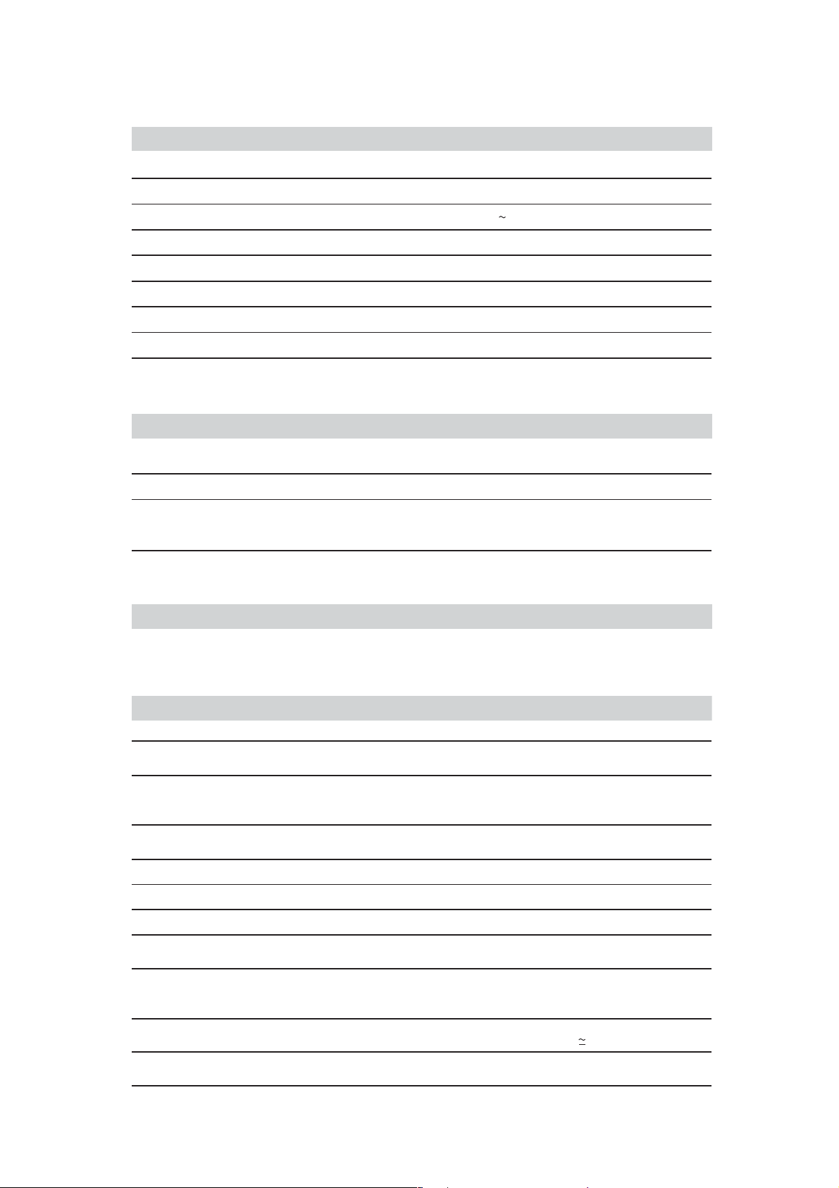
LASER BEAM SAFETY PRECAUTIONS
This DVD player uses a pickup that emits a laser beam.
Do not look directly at the laser beam coming
from the pickup or allow it to strike against your
skin.
The laser beam is emitted from the location shown in the figure. When checking the laser diode, be sure to keep
your eyes at least 30 cm away from the pickup lens when the diode is turned on. Do not look directly at the laser
beam.
CAUTION: Use of controls and adjustments, or doing procedures other than those specified herein, may result in
hazardous radiation exposure.
Drive Mechanism Assembly
Laser Beam Radiation
Laser Pickup
Turntable
Location: Inside Top of DVD mechanism.
1-2-1 R3PLSP
Page 6

IMPORTANT SAFETY PRECAUTIONS
Product Safety Notice
Some electrical and mechanical parts have special
safety-related characteristics which are often not evident from visual inspection, nor can the protection
they give necessarily be obtained by replacing them
with components rated for higher voltage, wattage,
etc. Parts that have special safety characteristics are
identified by a ! on schematics and in parts lists. Use
of a substitute replacement that does not have the
same safety characteristics as the recommended
replacement part might create shock, fire, and/or other
hazards. The Product’s Safety is under review continuously and new instructions are issued whenever
appropriate. Prior to shipment from the factory, our
products are carefully inspected to confirm with the
recognized product safety and electrical codes of the
countries in which they are to be sold. However, in
order to maintain such compliance, it is equally important to implement the following precautions when a set
is being serviced.
Precautions during Servicing
A. Parts identified by the ! symbol are critical for
safety. Replace only with part number specified.
B. In addition to safety, other parts and assemblies
are specified for conformance with regulations
applying to spurious radiation. These must also be
replaced only with specified replacements.
Examples: RF converters, RF cables, noise blocking capacitors, and noise blocking filters, etc.
C. Use specified internal wiring. Note especially:
1)Wires covered with PVC tubing
2)Double insulated wires
3)High voltage leads
D. Use specified insulating materials for hazardous
live parts. Note especially:
1)Insulation tape
2)PVC tubing
3)Spacers
4)Insulators for transistors
E. When replacing AC primary side components
(transformers, power cord, etc.), wrap ends of
wires securely about the terminals before soldering.
F. Observe that the wires do not contact heat produc-
ing parts (heatsinks, oxide metal film resistors, fusible resistors, etc.).
G. Check that replaced wires do not contact sharp
edges or pointed parts.
H. When a power cord has been replaced, check that
5 - 6 kg of force in any direction will not loosen it.
I. Also check areas surrounding repaired locations.
J. Be careful that foreign objects (screws, solder
droplets, etc.) do not remain inside the set.
K. Crimp type wire connector
The power transformer uses crimp type connectors
which connect the power cord and the primary side
of the transformer. When replacing the transformer,
follow these steps carefully and precisely to prevent shock hazards.
Replacement procedure
1)Remove the old connector by cutting the wires at a
point close to the connector.
Important: Do not re-use a connector. (Discard it.)
2)Strip about 15 mm of the insulation from the ends
of the wires. If the wires are stranded, twist the
strands to avoid frayed conductors.
3)Align the lengths of the wires to be connected.
Insert the wires fully into the connector.
4)Use a crimping tool to crimp the metal sleeve at its
center. Be sure to crimp fully to the complete closure of the tool.
L. When connecting or disconnecting the internal
connectors, first, disconnect the AC plug from the
AC outlet.
1-3-1 DVD_SFNP
Page 7
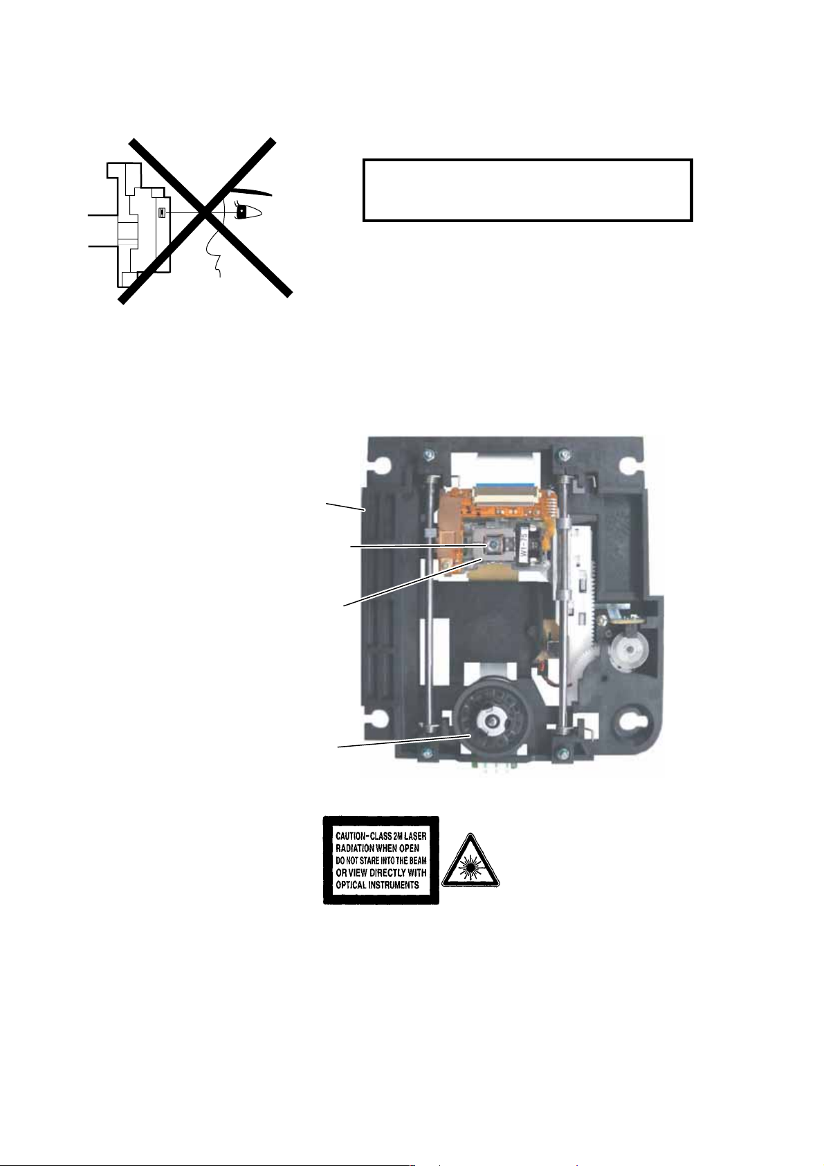
Safety Check after Servicing
Examine the area surrounding the repaired location
for damage or deterioration. Observe that screws,
parts, and wires have been returned to their original
positions. Afterwards, do the following tests and confirm the specified values to verify compliance with
safety standards.
1. Clearance Distance
When replacing primary circuit components, confirm
specified clearance distance (d) and (d’) between soldered terminals, and between terminals and surrounding metallic parts. (See Fig. 1)
Table 1 : Ratings for selected area
AC Line Voltage Clearance Distance (d), (d’)
220 to 240 V
Note: This table is unofficial and for reference only.
Be sure to confirm the precise values.
2. Leakage Current Test
≥ 3 mm(d)
≥ 6 mm(d’)
Chassis or Secondary Conductor
Primary Circuit
d' d
Fig. 1
Exposed Accessible Part
Confirm the specified (or lower) leakage current
between B (earth ground, power cord plug prongs)
and externally exposed accessible parts (RF terminals, antenna terminals, video and audio input and
output terminals, microphone jacks, earphone jacks,
etc.) is lower than or equal to the specified value in the
table below.
Measuring Method (Power ON) :
Insert load Z between B (earth ground, power cord
plug prongs) and exposed accessible parts. Use an
AC voltmeter to measure across the terminals of load
Z. See Fig. 2 and the following table.
Table 2: Leakage current ratings for selected areas
AC Line Voltage Load Z Leakage Current (i)
220 to 240 V
2kΩ RES.
Connected in
parallel
50kΩ RES.
Connected in
parallel
i≤0.7mA AC Peak
i≤2mA DC
i≤0.7mA AC Peak
i≤2mA DC
Z
One side of
B
Power Cord Plug Prongs
One side of power cord plug
AC Voltmeter
(High Impedance)
prongs (B) to:
RF or
Antenna terminals
A/V Input, Output
Fig. 2
Note: This table is unofficial and for reference only. Be sure to confirm the precise values.
1-3-2 DVD_SFNP
Page 8
STANDARD NOTES FOR SERVICING
NOTE: BOARD MEANS PRINTED CIRCUIT BOARD.
Circuit Board Indications
1. The output pin of the 3 pin Regulator ICs is
indicated as shown.
Top View
Out
2. For other ICs, pin 1 and every fifth pin are
indicated as shown.
Pin 1
3. The 1st pin of every male connector is indicated as
shown.
Pin 1
Input
In
Bottom View
5
10
Pb (Lead) Free Solder
When soldering, be sure to use the Pb free solder.
How to Remove / Install Flat Pack-IC
1. Removal
With Hot-Air Flat Pack-IC Desoldering Machine:
1. Prepare the hot-air flat pack-IC desoldering
machine, then apply hot air to the Flat Pack-IC
(about 5 to 6 seconds). (Fig. S-1-1)
Fig. S-1-1
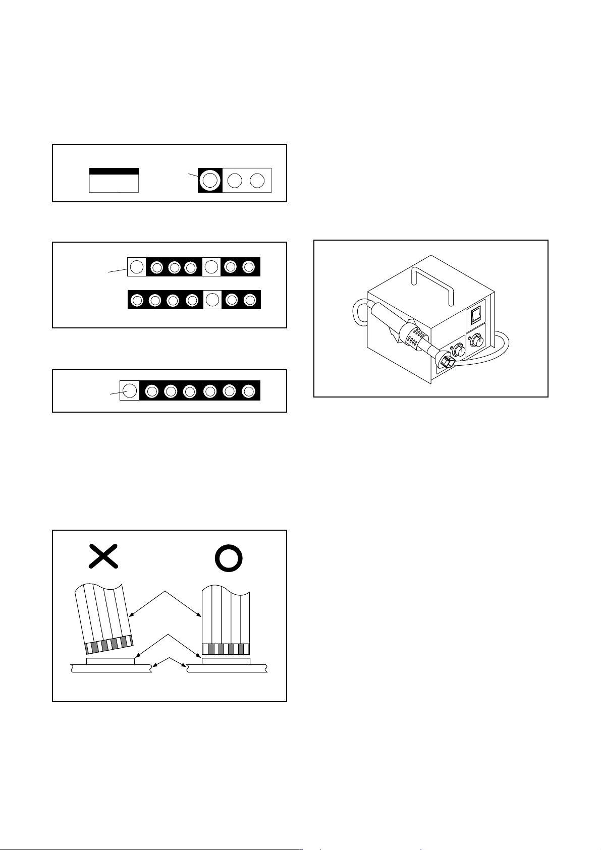
Instructions for Connectors
1. When you connect or disconnect the FFC (Flexible
Foil Connector) cable, be sure to first disconnect
the AC cord.
2. FFC (Flexible Foil Connector) cable should be
inserted parallel into the connector, not at an
angle.
FFC Cable
Connector
BOARD
* Be careful to avoid a short circuit.
2. Remove the flat pack-IC with tweezers while
applying the hot air.
3. Bottom of the flat pack-IC is fixed with glue to the
BOARD; when removing entire flat pack-IC, first
apply soldering iron to center of the flat pack-IC
and heat up. Then remove (glue will be melted).
(Fig. S-1-6)
4. Release the flat pack-IC from the BOARD using
tweezers. (Fig. S-1-6)
CAUTION:
1. The Flat Pack-IC shape may differ by models. Use
an appropriate hot-air flat pack-IC desoldering
machine, whose shape matches that of the Flat
Pack-IC.
2. Do not supply hot air to the chip parts around the
flat pack-IC for over 6 seconds because damage
to the chip parts may occur. Put masking tape
around the flat pack-IC to protect other parts from
damage. (Fig. S-1-2)
1-4-1 DVDN_SN
Page 9
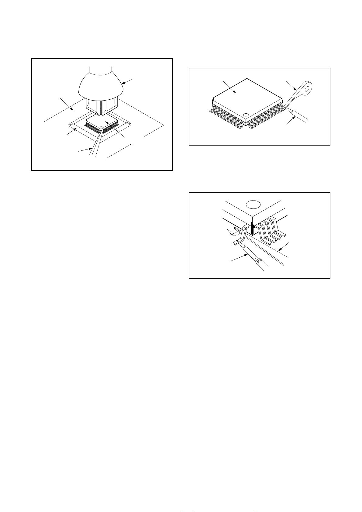
3. The flat pack-IC on the BOARD is affixed with
glue, so be careful not to break or damage the foil
of each pin or the solder lands under the IC when
removing it.
With Soldering Iron:
1. Using desoldering braid, remove the solder from
all pins of the flat pack-IC. When you use solder
flux which is applied to all pins of the flat pack-IC,
you can remove it easily. (Fig. S-1-3)
BOARD
Masking
Tape
Tweezers
Hot-air
Flat Pack-IC
Desoldering
Machine
Flat Pack-IC
Fig. S-1-2
Flat Pack-IC
Desoldering Braid
Soldering Iron
Fig. S-1-3
2. Lift each lead of the flat pack-IC upward one by
one, using a sharp pin or wire to which solder will
not adhere (iron wire). When heating the pins, use
a fine tip soldering iron or a hot air desoldering
machine. (Fig. S-1-4)
Sharp
Pin
Fine Tip
Soldering Iron
3. Bottom of the flat pack-IC is fixed with glue to the
BOARD; when removing entire flat pack-IC, first
apply soldering iron to center of the flat pack-IC
and heat up. Then remove (glue will be melted).
(Fig. S-1-6)
4. Release the flat pack-IC from the BOARD using
tweezers. (Fig. S-1-6)
Fig. S-1-4
1-4-2 DVDN_SN
Page 10

With Iron Wire:
1. Using desoldering braid, remove the solder from
all pins of the flat pack-IC. When you use solder
flux which is applied to all pins of the flat pack-IC,
you can remove it easily. (Fig. S-1-3)
2. Affix the wire to a workbench or solid mounting
point, as shown in Fig. S-1-5.
3. While heating the pins using a fine tip soldering
iron or hot air blower, pull up the wire as the solder
melts so as to lift the IC leads from the BOARD
contact pads as shown in Fig. S-1-5.
4. Bottom of the flat pack-IC is fixed with glue to the
BOARD; when removing entire flat pack-IC, first
apply soldering iron to center of the flat pack-IC
and heat up. Then remove (glue will be melted).
(Fig. S-1-6)
5. Release the flat pack-IC from the BOARD using
tweezers. (Fig. S-1-6)
Note: When using a soldering iron, care must be
taken to ensure that the flat pack-IC is not
being held by glue. When the flat pack-IC is
removed from the BOARD, handle it gently
because it may be damaged if force is applied.
Hot Air Blower
2. Installation
1. Using desoldering braid, remove the solder from
the foil of each pin of the flat pack-IC on the
BOARD so you can install a replacement flat packIC more easily.
2. The “●” mark on the flat pack-IC indicates pin 1.
(See Fig. S-1-7.) Be sure this mark matches the 1
on the BOARD when positioning for installation.
Then presolder the four corners of the flat pack-IC.
(See Fig. S-1-8.)
3. Solder all pins of the flat pack-IC. Be sure that
none of the pins have solder bridges.
Example :
Pin 1 of the Flat Pack-IC
is indicated by a " " mark.
Fig. S-1-7
To Solid
Mounting Point
BOARD
Tweezers
Iron Wire
Soldering Iron
Fig. S-1-5
Fine Tip
Soldering Iron
Flat Pack-IC
or
Presolder
Flat Pack-IC
BOARD
Fig. S-1-8
Fig. S-1-6
1-4-3 DVDN_SN
Page 11
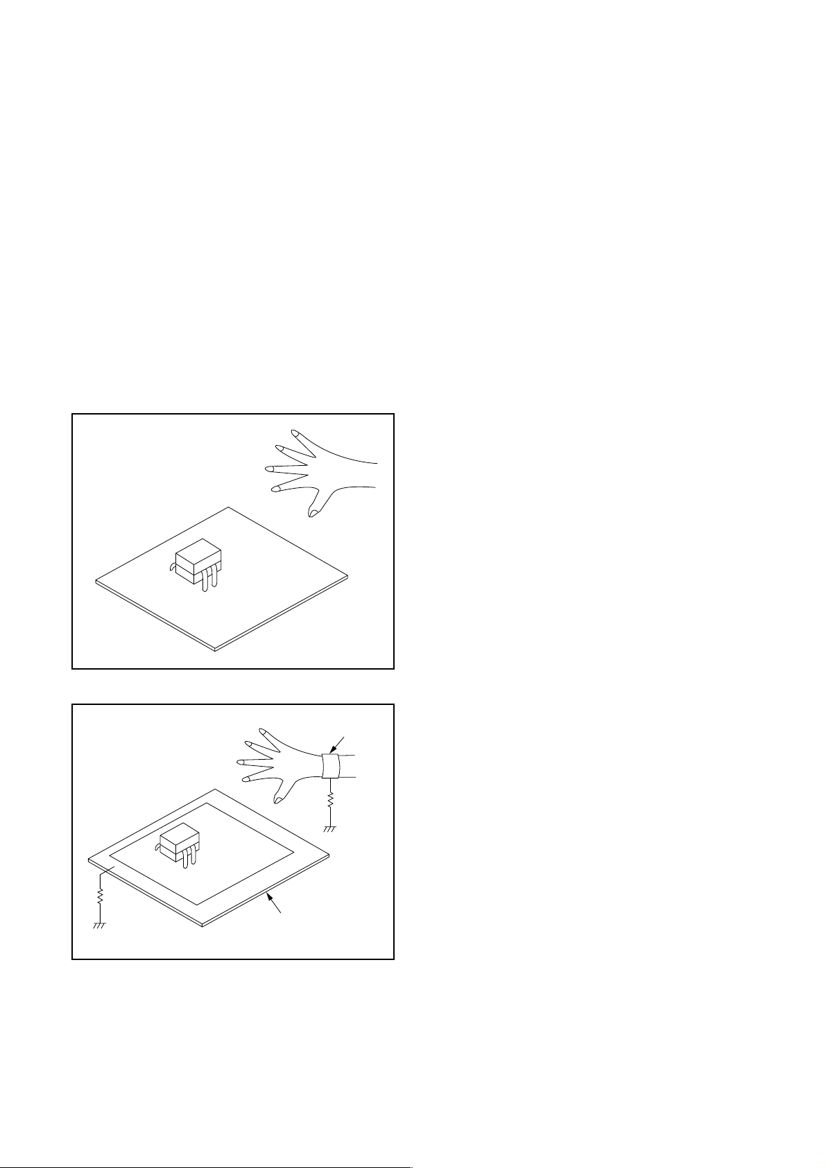
Instructions for Handling Semiconductors
Electrostatic breakdown of the semi-conductors may
occur due to a potential difference caused by
electrostatic charge during unpacking or repair work.
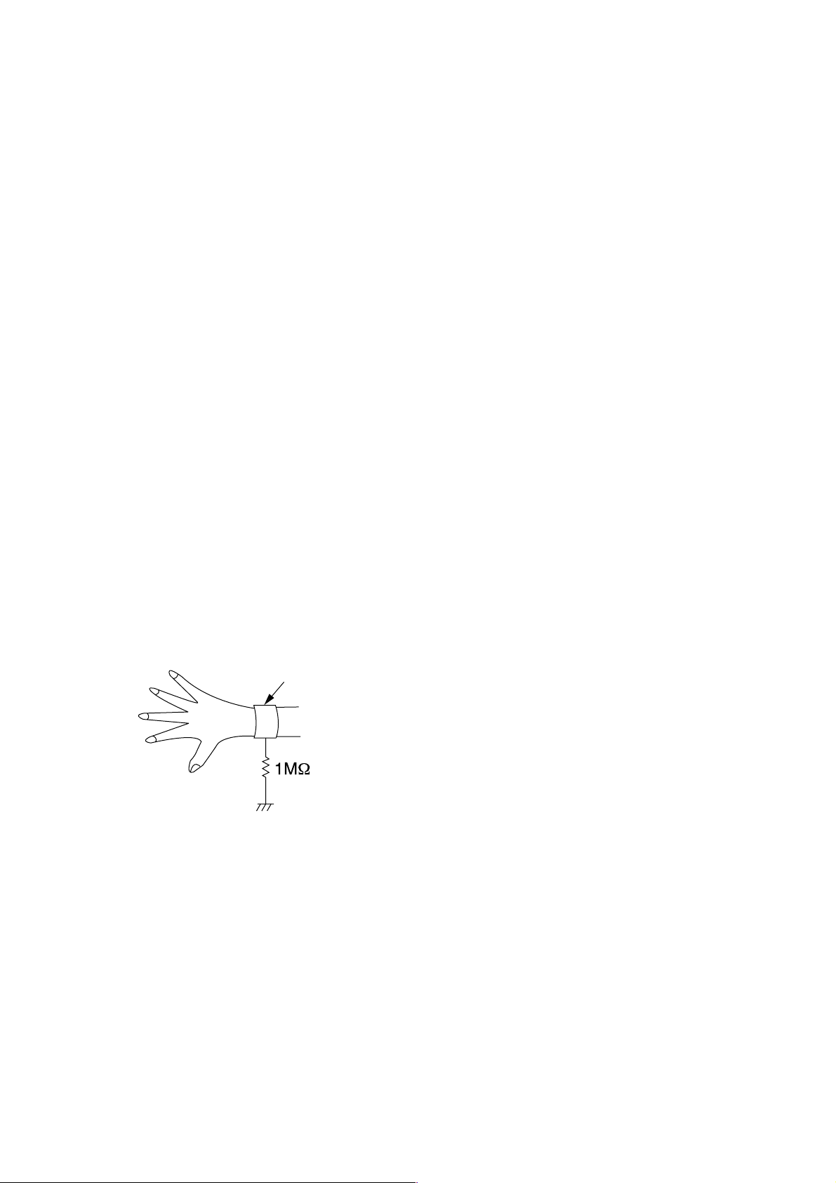
1. Ground for Human Body
Be sure to wear a grounding band (1 MΩ) that is
properly grounded to remove any static electricity that
may be charged on the body.
2. Ground for Workbench
Be sure to place a conductive sheet or copper plate
with proper grounding (1 MΩ) on the workbench or
other surface, where the semi-conductors are to be
placed. Because the static electricity charge on
clothing will not escape through the body grounding
band, be careful to avoid contacting semi-conductors
with your clothing.
<Incorrect>
<Correct>
1MΩ
BOARD
Grounding Band
1MΩ
BOARD
Conductive Sheet or
Copper Plate
1-4-4 DVDN_SN
Page 12
HANDLING PRECAUTIONS FOR HDD
CAUTION:
1. SHOCK
a. Exposing HDD to shock may be the biggest
damaging factor. Please note that HDD is easily
damaged even if dropped from any height. Be sure
to place HDD on a shock-absorbent mat. Also, be
careful when transporting HDD.
b. Be careful not to subject HDD to any shock when
tightening screws for HDD replacement.
(Tighten screws manually, not with an electric
driver.)
2. MOISTURE
a. Moisture may also be a damaging factor. HDD is
semiclosed style. Sudden changes in ambient
temperature may cause moisture to form. Monitor
temperature and do not allow moisture to form on
the media surface. Also, when opening HDD
package, do so only after package is at ambient
temperature.
b. After replacing HDD, leave it to reach room
temperature (about 2 hours) for preventing dew
internal condensation, and then work necessary
task such as operation check.
4. OTHERS
a. Be careful so as not to do the followings.
Otherwise, HDD might be damaged.
- DO NOT disassemble HDD.
- When handling HDD, be sure to hold both sides
securely.
b. HDD should be stored, packed in the protective
bag, in suitable surroundings (i.e., no extreme
changes in temperature to avoid condensation).
c. When transporting HDD, be sure to use the
exclusive packing case (the replacement HDD
carton).
d. Do not stack HDDs.
e. Do not place vertically because HDD is unstable
and easy to fall.
3. STATIC ELECTRICITY
a. After removing HDD or taking replacement HDD
out of the protective bag (the replacement HDD is
packed in a protective bag), place HDD on a
conductive surface. A grounding band should be
worn when handling.
Grounding Band
Both the conductive surface and grounding band
should be grounded.
b. Make sure that HDD is placed on main unit
completely and then let go of it, when assembling.
c. Do not put HDD on a packing bag. (for preventing
electrostatic damage)
1-5-1 DHD_SN
Page 13
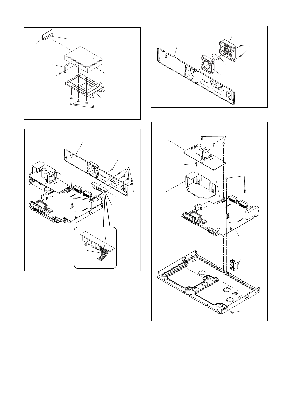
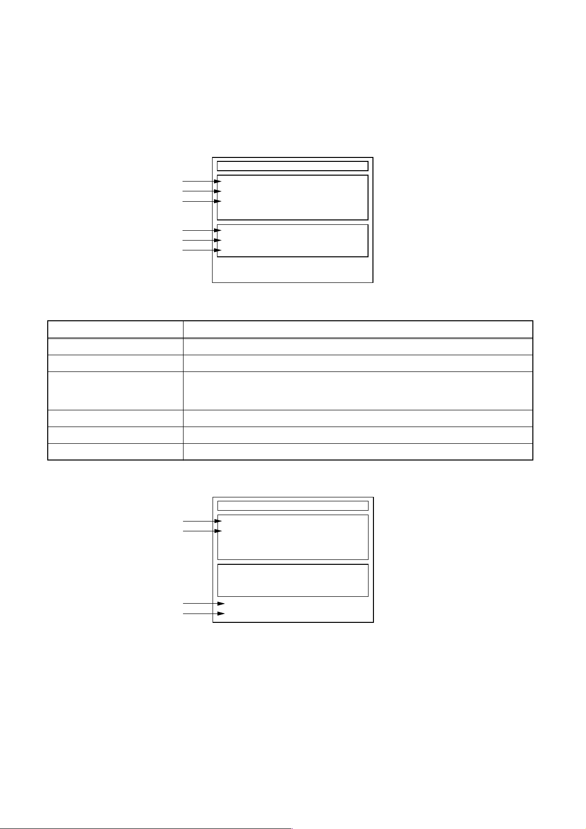
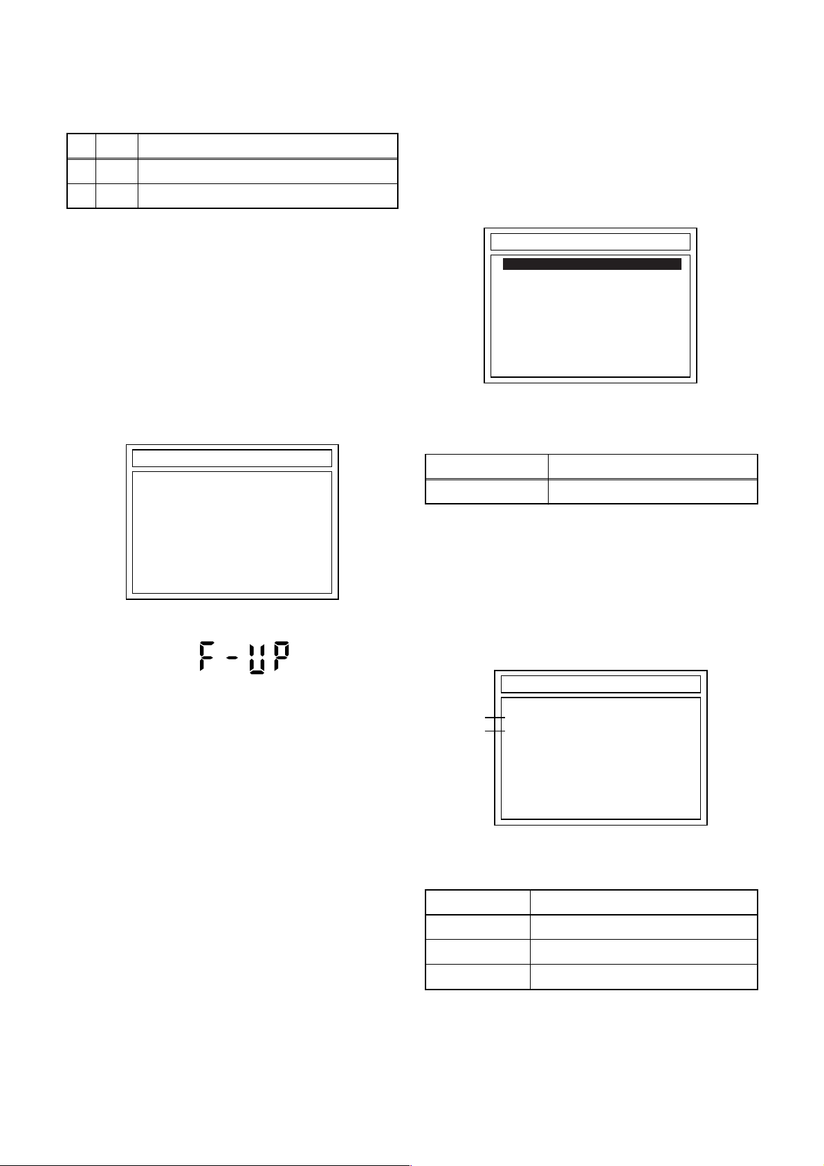
CABINET DISASSEMBLY INSTRUCTIONS
NOTE: BOARD MEANS PRINTED CIRCUIT BOARD.
1. Disassembly Flowchart
This flowchart indicates the disassembly steps to gain
access to item(s) to be serviced. When reassembling,
follow the steps in reverse order. Bend, route, and
dress the cables as they were originally.
[1] Cover Top
[18] Front
Bracket R
[5] HDD Assembly
[7] BOARD ATA
[8] HDD Bracket
[9] HDD
[4] BOARD
CONTROL
[10] Panel Rear
Unit
[11] BOARD JACK
[12] Cover Fan
[13] DC Fan Motor
[14] Panel Rear
[2] Front Unit
[3] Front Assembly
[6] DVD Mechanism
& DVD/HDD MAIN
BOARD Assembly
[15] BOARD
POWER SUPPLY
[16] Power Holder
[17] BOARD
POWER
ID/
LOC.
PART
No.
[9] HDD D5
Panel Rear
[10]
Unit
BOARD
[11]
JACK
REMOVE/*UNHOOK/
Fig.
UNLOCK/RELEASE/
No.
UNPLUG/DESOLDER
Note
(S-6), HDD Plate
Earth
*CN1601, 4(S-7),
D6
2(S-8)
D6 *CN1802, Desolder ---
[12] Cover Fan D7 2(S-9) ---
REMOVAL
DC Fan
[13]
Motor
D7 Earth Fan ---
[14] Panel Rear D7 ---------- ---
BOARD
[15]
POWER
D8 *CN1151, 4(S-10) ---
SUPPLY
Power
[16]
[17]
Holder
BOARD
POWER
D8 ---------- ---
D8 2(S-11) ---
---
---
2. Disassembly Method
ID/
LOC.
No.
PART
Fig.
No.
[1] Cover Top D1 8(S-1) ---
[2] Front Unit D2
Front
[3]
[4]
[5]
Assembly
BOARD
CONTROL
HDD
Assembly
D3 ---------- ---
D3 *3(L-3) 1-3
D4
DVD
Mechanism
[6]
& DVD/
HDD MAIN
D4
BOARD
Assembly
BOARD
[7]
ATA
D5 CN3001 ---
REMOVAL
REMOVE/*UNHOOK/
UNLOCK/RELEASE/
UNPLUG/DESOLDER
CN1641, *5(L-1),
*3(L-2)
*CN651, *CN1015,
4(S-2)
2(S-3), 4(S-4),
*CN101, *CN701,
Locking Card Spacer,
Attachment Holder
Note
1
1-1
1-2
---
2
Front
[18]
↓
(1)
Bracket R
↓
(2)
D8 (S-12) ---
↓
(3)
↓
(4)
(5)
Note:
(1): Identification (location) No. of parts in the figures
(2): Name of the part
(3): Figure Number for reference
(4): Identification of parts to be removed, unhooked,
unlocked, released, unplugged, unclamped, or
desoldered.
P=Spring, L=Locking Tab, S=Screw,
CN=Connector
*=Unhook, Unlock, Release, Unplug, or Desolder
e.g. 6(S-1) = six Screws (S-1),
5(L-1) = five Locking Tabs (L-1)
(5): Refer to “Reference Notes.”
↓
[8]
HDD
Bracket
D5 4(S-5) ---
1-6-1 E2B10DC
Page 14

Reference Notes
1. Locking Tabs (L-1) ,(L-2) and (L-3) are fragile. Be
careful not to break them.
1-1. Release five Locking Tabs (L-1).
1-2. Release three Locking Tabs (L-2) and
remove the Front Assembly.
1-3. Release three Locking Tabs (L-3).
2. Do not replace the DVD Mechanism or the DVD/
HDD MAIN BOARD Assembly separately, when
replacing the DVD Mechanism & DVD/HDD MAIN
BOARD Assembly. Order the new DVD
Mechanism & DVD/HDD MAIN BOARD Assembly.
2-1. Whenever you have replaced the HDD unit,
initialize the HDD unit. To initialize the HDD
unit, perform the following.To put the HDD &
DVD into the HDD mode, press the [HDD]
button on the remote control unit.
2-2. To put the HDD & DVD into the self-check
mode, after pressing [VARIABLE SKIP]
button, press the [3], [6], and [9] buttons on
the remote control in that order within three
seconds.
2-3. Press [ENTER] button. The HDD & DVD is
initialized and the power is turned off
automatically after two seconds.
(L-1)
(L-2)
(L-1)
(L-1)
CN1641
[2] Front Unit
Fig. D2
[4] BOARD
CONTROL
[1] Cover Top
(S-1)
(S-1)
(S-1)
Fig. D1
[3] Front Assembly
Attachment
Holder
(S-4)
CN1015
(S-3)
(L-3)
Fig. D3
[6] DVD Mechanism
& DVD/HDD MAIN
BOARD Assembly
CN651
CN101
CN701
[5] HDD
Assembly
(S-2)
Locking Card Spacer
Fig. D4
1-6-2 E2B10DC
Page 15
[7] BOARD ATA
HDD Plate Earth
CN3001
[12] Cover Fan
[14] Panel Rear
(S-9)
Earth Fan
(S-6)
(S-5)
[9] HDD
[8] HDD Bracket
[10] Panel Rear Unit
CN1601
Fig. D5
(S-8)
(S-7)
(S-8)
CN1802
[11] BOARD
JACK
[15] BOARD
POWER SUPPLY
(S-10)
[16] Power
Holder
CN1151
[13] DC Fan Motor
Fig. D7
(S-10)
(S-11)
Lead
with
blue
stripe
Desolder
Fig. D6
[17] BOARD
POWER
[18] Front
Bracket R
(S-12)
Fig. D8
1-6-3 E2B10DC
Page 16
HOW TO SELF-CHECK AND INITIALIZE THE HDD & DVD
1. Turn on the HDD & DVD.
2. To put the HDD & DVD into the HDD mode, press [HDD] on the remote control unit.
3. To put the HDD & DVD into the self-check mode, after pressing [VARIABLE SKIP] button, press the [3], [6],
and [9] buttons on the remote control in that order within three seconds.
Fig. a appears on the screen and all LEDs light.
"
" differs depending on the models.
*******
Self-Analysys and Report
*1
*2
*3
DVD CONNECT STATUS :
HDD CONNECT STATUS :
HDD POWER ON HOURS :
*4
*5
*6
BE Ver. :
FE Ver. :
Sub Micon Ver. :
T2*******Q2J
R20_0**_***h
NFQ2***T1-3N11
Fig. a: Self-Check Mode Screen
Table 1: Description of Fig. a
INDICATION DESCRIPTION
DVD CONNECT STATUS (*1) Connecting Condition of DVD(F/E)
HDD CONNECT STATUS (*2) Connecting Condition of HDD
Value of HDD power on hours obtained from S.M.A.R.T. command. (If not obtainable,
HDD POWER ON HOURS (*3)
value of HDD power on hours is “0”.)
Value in parentheses is the factory setting value. (If no setting, the value is “0”.)
BE Ver. (*4) B/E version
FE Ver. (*5) F/E version
Sub Micon Ver. (*6) Sub micro controller version
4. Upon the self-check completion, Fig. b appears on the screen.
"
" differs depending on the models.
*******
Self-Analysys and Report
*7
*8
DVD CONNECT STATUS : OK
HDD CONNECT STATUS : OK
HDD POWER ON HOURS : 100(40)
T2*******Q2J
R20_0**_***h
NFQ2***T1-3N11
ENTER
POWER
*10
BE Ver. :
FE Ver. :
Sub Micon Ver. :
*9
FACTORY DEFAULT :
POWER OFF :
Fig. b: Screen of Finishing Self-Check Mode
1-7-1 E2B10INT
Page 17

Table 2: Indication of DVD self-check (*7)
INDICATION DESCRIPTION
OK Connection of DVD is normal.
NOT FOUND DVD drive cannot be found.
CABLE ERROR
FFC cable (connecting to CN401) between the DVD drive and the DVD/HDD MAIN BOARD
is not connected correctly.
Table 3: Indication of HDD self-check (*8)
INDICATION DESCRIPTION
OK Connection of HDD is normal.
NOT FOUND HDD drive cannot be found.
CABLE ERROR FFC cable between the BOARD ATA and the HDD drive is not connected correctly.
Table 4: Available button in self-check mode
BUTTON DESCRIPTION
ENTER (*9) Initialize (only when the self-check mode is complete)
ON / STANDBY (*10) Turn the power off (when the self-check mode is complete)
OTHER Not available
5. When the self-check mode is complete, press [ ] button to turn the power off.
When initializing the HDD & DVD, press [ENTER] button. Fig. c appears on the screen. After two seconds, the
power is turned off automatically.
"
" differs depending on the models.
*******
Self-Analysys and Report
DVD CONNECT STATUS : OK
HDD CONNECT STATUS : OK
HDD POWER ON HOURS : 100(40)
BE Ver. :
FE Ver. :
Sub Micon Ver. :
FACTORY DEFAULT : *11WRITING
T2*******Q2J
R20_0**_***h
NFQ2***T1-3N11
Fig. c: Initialize Mode Screen
Table 5: Description of *11 in Fig. c
INDICATION DESCRIPTION
ENTER Initialization preparation is complete.
WRITING Initializing
OK Initializing is finished normally.
NG Initializing is not finished normally.
NOTE: When initializing, “Current Clock”, “Setup Changing Item”, “Channel Setup”, “Area Setup”, “Program” and
“HDD Contents” are initialized.
1-7-2 E2B10INT
Page 18
FIRMWARE RENEWAL MODE
1. Update Contents
Item Status
1 B/E Update B/E FIRMWARE
2 F/E Update F/E FIRMWARE
2. Update
1. Turn the power on and remove the disc in the tray.
2. To switch the HDD & DVD into the HDD mode,
press [HDD] on the remote control unit.
3. To put the HDD & DVD into version up mode,
press [VARIABLE SKIP] and [6], [5], [4] buttons on
the remote control unit in that order within 3
seconds. The tray will open automatically.
Fig. a appears on the TV screen and Fig. b
appears on the VFD.
*FIRMWARE version will differ depending on the
model. Fig. a is an example.
DISC UPDATE
4. Load the update disc.
The TV screen will display Fig. c.
- If the update disc contains only a single file, the
update will initiate automatically when the disc is
inserted.
*FIRMWARE version will differ depending on the
model. Fig. c is an example.
DISC UPDATE
H3T00141B2C.MOT
<DIR> BE
<DIR> FE
Fig. c: Update Disc TV Screen
Effective FIRMWARE update files will have the file
extensions shown below.
File extension Status
MOT F/E FIRMWARE file
Please Insert F/W Disc
Fig. a: Update Mode TV Screen
Fig. b: VFD Display in Update Mode
5. Select the desired FIRMWARE to be updated with
the arrow button and press the [ENTER] or [PLAY]
button.
The tray will open automatically; close the tray by
pressing [OPEN/CLOSE] button or by hand.
6. Fig. d appears on the TV screen and Fig. e
appears on the VFD, and the update will start.
*FIRMWARE version will differ depending on the
model. Fig. d is an example.
DISC UPDATE
*1
TARGET: B/E
*2
STATUS: EXECUTING
DISC UPDATING
Fig. d: TV Display during update
The status displayed in *1 is as shown below.
Display Status
B/E FIRMWARE B/E
F/E FIRMWARE F/E
UNKNOWN Not FIRMWARE B/E or F/E
1-8-1 E2B10FW
Page 19
The status displayed in *2 is as shown below.
Display Status
EXECUTING
Loading F/W from Update Disc or
writing to Flash memory
ERROR Error during Flash memory writing
FILE ERROR Check SAM error in F/W file
READ ERROR Error during F/W file reading
3. How to Verify the Firmware
Version
1. Turn the power on and remove the disc in the tray.
2. To switch the HDD & DVD into HDD mode, press
[HDD] on the remote control unit.
3. To put the HDD & DVD into version display mode,
press [VARIABLE SKIP] and [1], [2], [3] buttons on
the remote control unit in that order within 3
seconds. Fig. i appears on the TV screen.
******* part will differ depending on the model.
Fig. i is an example.
Fig. e: VFD Display during update
When the TV screen displays "Firmware
Updating... XX% Complete," the VFD will indicate
"XX"%.
7. When update is complete, the unit will shut off
automatically.
8. If an error occured during updating, the TV screen
will display Fig. f.
*FIRMWARE version will differ depending on the
model. Fig. f is an example.
DISC UPDATE
TARGET: B/E
STATUS: ERROR
PLEASE PUSH POWER BUTTON
Fig. f: TV Display when completing update with error
Fig. h: VFD Display when completing update with error
In this case, all button operations will be invalid
except [ ] button.
9. Press [ ] button to turn the power off and press
[ ] button again to turn the power back on and
finish updating.
VERSION INFORMATION
Model Name :
BE Ver. :
FE Ver :
Sub Micon Ver. :
REGION:
CPRM KEY NO:
HDD MODEL:
DivX Ver.:
LD ADJUSTMENT:
DISC ADJUSTMENT:
E2B10ED
H3T*****B2C
R34_***_**
T3007THP
2
(0x***)
***********(***GByte)
***
OK
OK
Fig. i: Firmware version display
Display Contents
MODEL NAME Product number
BE Ver. Firmware B/E version
FE Ver. Application F/E version
Sub Micon Ver.
Sub Microcontroller firmware
version
REGION Region code of playable DVD disc
CPRM KEY
NO.
HDD MODEL
LD
ADJUSTMENT
DISC
ADJUSTMENT
CPRM key number
HDD serial number and capacity
(GByte)
LD adjustment progress (done: OK/
not done: --)
Factory adjustment progress (done:
OK/not done: --)
Effective buttons in this mode are the following...
Buttons Operations
POWER
SETUP
TOP MENU
Power off to release from this
mode.
Version display disappears and
SETUP screen appears.
Version display disappears and
TOP MENU screen appears.
Version display disappears and
TIMER PROG.
TIMER PROGRAMMING screen
appears.
DUBBING
MENU
Others
Version display disappears and
DUBBING screen appears.
While displaying version and
normal operation.
1-8-2 E2B10FW
Page 20
FLOW CHART NO.1
The power cannot be turned on.
TROUBLESHOOTING
NOTE: BOARD MEANS PRINTED CIRCUIT BOARD.
Is the fuse normal?
Ye s
Is normal state restored when once unplugged
power cord is plugged again after several seconds.
Ye s
Is the EV+5V line voltage normal?
Ye s
Check each rectifying circuit of secondary circuit
and service it if defective.
FLOW CHART NO.2
The fuse blows out.
Check the presence that the primary component
is leaking or shorted and service it if defective.
After servicing, replace the fuse.
FLOW CHART NO.3
When the output voltage fluctuates.
No
No
No
See FLOW CHART No.2 <The fuse blows out.>
Check for lead or short-circuiting of primary
circuit component and service it if defective.
(Q2101,Q2102,T2001,D2104)
Check the presence that the rectifying diode or circuit
is shorted in each rectifying circuit of secondary side
and service it if defective.
Does the secondary side photo coupler circuit
operate normally?
Ye s
Check the circuit and service it if defective.
(IC2101, D2113, D2110)
FLOW CHART NO.4
When buzz sound can be heard in the vicinity of power circuit.
Check if there is short circuit on the rectifying diode and the circuit in each rectifying circuit of secondary side and
service it if defective. (D2201,D2202,D2203,D2204,D2205,D2206,D2207,D2208,D2209,IC1151,IC1152,IC1025,
IC1002,Q1015,Q1508,Q1160,Q1163,Q2203,Q1154,Q1159)
FLOW CHART NO.5
-FL is not outputted.
Is the supply voltage of -30V fed to the anode of
D2201?
Ye s
Check for load circuit short-circuiting or leak, and
service it if defective.
No
No
Check the circuit and service it if defective.
(IC2101, IC2201,D2213)
Check D2201 and their periphery, and service it if
defective.
1-9-1 E2B10TR
Page 21
FLOW CHART NO.6
HDD+12V is not outputted.
Is 14V voltage supplied to the collector of Q2203?
No
Ye s
Is the "H" pulse inputted to
the base of Q1016?
No
Ye s
Check Q2221,IC2204,D2225 and their periphery,
and service it if defective.
FLOW CHART NO.7
P-ON+10V is not outputted. (HDD+12V is outputted normally.)
Is 11V voltage supplied to the base of Q1160?
No
Ye s
Replace Q1160.
FLOW CHART NO.8
EV +10.5V is not outputted.
Is HDD+12V outputted normally?
No
Ye s
Replace Q1163.
Check D2204, D2205, D2212, C2204 and their
periphery, and service it if defective.
Check the line between the base of Q1016 and
Pin (77) of IC1501,and service it if defective.
Check D1162 and their periphery, and service
it if defective.
See FLOW CHART No.6
<HDD+12V is not outputted.>
FLOW CHART NO.9
AL+9V is not outputted.
Is 12V voltage supplied to Pin (3) of IC1002?
Ye s
Replace IC1002.
FLOW CHART NO.10
AL+5V(1) is not outputted.
Check D2206,D2207,D2213,C2205,C2216 and
their periphery, and service it if defective.
FLOW CHART NO.11
AL+5V is not outputted. (AL+9V is outputted normally.)
Is 7V voltage supplied to the
collector
of Q1508?
Ye s
Is 5.6V voltage supplied to the base of Q1508?
Ye s
Replace Q1508.
No
No
No
Check D1170, D1171, D2205, D2212, C2204
and their periphery, and service it if defective.
Check D1172, D1173 and their periphery, and
service it if defective.
Check D1508 and their periphery, and service it if
defective.
1-9-2 E2B10TR
Page 22
FLOW CHART NO.12
P-ON+5V is not outputted. (P-ON+10V is outputted normally.)
Is 5V voltage supplied to the
Is the "H" pulse inputted to
Replace Q1154.
FLOW CHART NO.13
SYS +5V is not outputted.
Is 12V voltage inputted to Pin (3) of IC1025?
Replace IC1025.
FLOW CHART NO.14
EV+32V is not outputted.
Is the supply voltage 44V fed the cathode of D2202?
Check D1701 and their periphery and service it
if defective.
FLOW CHART NO.15
AUDIO +5V is not outputted. (P-ON+10V is outputted normally.)
collector
Ye s
the base of Q1154?
Ye s
Ye s
Ye s
of Q1154?
No
No
No
No
Check D2206, D2207, D2213, C2205, C2216 and
their periphery, and service it if defective.
Check R1162, R1166 and their periphery, and
service it if defective.
Check D1027, D2204, D2205, D2212, C2204 and
their periphery, and service it if defective.
Check D2202, C2202 and their periphery, and
service it if defective.
Is 6V voltage supplied to the base of Q1163?
Ye s
Replace Q1163.
FLOW CHART NO.16
EV+3.3V is not outputted. (SYS+5V is outputted normally.)
Is the voltage of approximately 4V supplied to
the base of Q1159?
Ye s
Replace Q1159.
FLOW CHART NO.17
P-ON+2.5V is not outputted.
Is 5V voltage supplied to Pin(1) of IC1151?
Ye s
Replace IC1151.
FLOW CHART NO.18
P-ON+3.3V is not outputted.
Is 5V voltage supplied to Pin(1) of IC1152?
Ye s
Replace IC1152.
No
No
No
No
Check D1163, C1168 and their periphery, and
service it if defective.
Check IC1153 and their periphery, and service it if
defective.
Check D2209, C2217 and their periphery, and
service it if defective.
Check D2209, C2217 and their
periphery, and service it if defective.
1-9-3 E2B10TR
Page 23
FLOW CHART NO.19
VI +1.2V is not outputted.
Check D2203, C2203 and their periphery, and
service it if defective.
FLOW CHART NO.20
The fluorescent display tube does not light up.
Is 5V voltage supplied to Pin(6, 24) of IC1503?
Ye s
Is approximately -23V to -28V voltage supplied to
Pin(15) of IC1503?
Ye s
Is there approximately 500kHz oscillation to
Pin(26) of IC1503?
Ye s
Are the filament voltage applied between (1)
and (24) of the fluorescent display tube?
Also negative voltage applied between these pins
and GND?
Ye s
Replace the fluorescent display tube.
FLOW CHART NO.21
The key operation is not functioning.
Are the contact point and the installation state of
the key switches normal?
Ye s
Is the control voltage normally inputted into
Pin(82, 83) of IC1501?
Ye s
Replace IC1501 or DVD MECHANISM & DVD
MAIN BOARD ASSEMBLY.
No
No
No
No
No
No
Check the SYS+5V line and service it if defective.
Check the -FL line and service it if defective.
Check R1560, IC1503 and their periphery, and
service it if defective.
Check the power circuit, D2208, D2215, C2207,
C2208 and their periphery, and service it if
defective.
Re-install some key switches correctly or
replace some key switches.
Check the key switches and their periphery, and
service it if defective.
KEYTerminal voltage of IC1501-82,83 -1
2.39
1.98
1.27
0.92
0.51
(V)
IC1501-82
REC
CH UP
REC
SPEED
CH
DOWN
POWER
IC1501-83
----------
REW
FWD
STOP
PLAY
POWER
KEY-2
1-9-4 E2B10TR
Page 24

FLOW CHART NO.22
No operation is possible from the remote control unit. (
Operation is possible from the unit.)
Is 5V voltage supplied to the Pin(3) terminal of
the RM1501 (remote control receiver)?
Ye s
Is the "L" pulse sent out from Pin(1) terminal of
the RM1501 (remote control receiver) when the
remote control unit is activated?
Ye s
Is the "L" pulse signal supplied to the Pin(3) of
IC1501?
Ye s
Replace IC1501 or DVD MECHANISM & DVD
MAIN BOARD ASSEMBLY.
FLOW CHART NO.23
The disc tray cannot be opened and closed. (It can be done using the remote control unit.)
Is the normal control voltage inputted to Pin(83) of
IC1501?
operation is not functioning.>
Replace the DVD MECHANISM & DVD MAIN
BOARD ASSEMBLY.
Refer to "FLOW CHART NO.21" <The key
Ye s
No
No
No
No
Check SYS+5V line and service it if defective.
Replace the RM1501 (remote control receiver).
Or replace remote control unit.
Check the line between the RM1501 (remote
control receiver) and the Pin(3) of IC1501, and
service it if defective.
Replace the "OPEN/CLOSE" button (SW1643).
FLOW CHART NO.24
[No Disc] indicated.
Both functions of picture and sound do not operate normally.
Replace the DVD MECHANISM & DVD MAIN
BOARD ASSEMBLY.
FLOW CHART NO.25
VIDEO E-E does not appear normally.
Are the video signals inputted to each pin of
IC1201?
IC1201 VIDEO-IN 1 (AV1)16PIN
IC1201 VIDEO-IN 1 (FRONT)14PIN
IC1201 Y-IN 1 (FRONT)7PIN
IC1201 C-IN 1 (FRONT)9PIN
IC1201 VIDEO-IN 2 (AV2)12PIN
IC1201 TUNER-VIDEO
Are the video signals outputted to each pin of
IC1201?
IC1201 VIDEO-Y/CVBS-IN61PIN
IC1201 VIDEO-C-IN59PIN
Are the video signals outputted to each pin of
CN1201?
CN1201 VIDEO-Y/CVBS-IN10PIN
CN1201 VIDEO-C-IN8PIN
20PIN
Ye s
Ye s
No
No
No
Check the line between video input terminal and
each pin of IC1201.
IC1201 → JK120616PIN
IC1201 → JK12127PIN
IC1201 → JK12129PIN
IC1201 → JK200112PIN
IC1201 → TU170120PIN
Is 5V voltage supplied to the Pin(27,29,47,63) of IC1201?
Ye s
Replace IC1201. Check AL+5V(2) line
and service it if defective.
Check the line between each pin of IC1201 and
each pin of CN1201 and service it if defective.
IC1201
IC1201
→ CN120161PIN
→ CN1201 59PIN
VIDEO-IN 1 (AV1)
VIDEO-IN 1 (
Y-IN 1 (FRONT)
C-IN 1 (FRONT)
VIDEO-IN 2 (AV2)
17PIN
TUNER-VIDEO
10PIN
8PIN
FRONT
)IC1201 → JK120114PIN
No
VIDEO-Y/CVBS-IN
VIDEO-C-IN
Continued to A on the next page.
1-9-5 E2B10TR
Page 25

A
Are the video signals outputted to each pin of
CN1201?
CN1201 VIDEO-Y(I/P)-OUT24PIN
CN1201 VIDEO-Y(I)-OUT30PIN
CN1201 VIDEO-Cr/Pr-OUT26PIN
CN1201 VIDEO-Cb/Pb-OUT28PIN
CN1201 VIDEO-C-OUT
Are the video signals shown above inputted into
each pin of IC1201?
IC1201 VIDEO-Y(I/P)-OUT51PIN
IC1201 VIDEO-Y(I)-OUT55PIN
IC1201 VIDEO-Cr/Pr-OUT52PIN
IC1201 VIDEO-Cb/Pb-OUT53PIN
IC1201 VIDEO-C-OUT57PIN
Are the video signals outputted to each pin of
IC1201?
IC1201 VIDEO-Y40PIN
IC1201 VIDEO-Cr/Pr39PIN
IC1201 VIDEO-Cb/Pb38PIN
IC1201 VIDEO-Y(YC)36PIN
IC1201 VIDEO-C(YC)34PIN
IC1201 VIDEO-OUT 1 (AV1)30PIN
IC1201 VIDEO-OUT 2 (AV2)22PIN
Are the video signals outputted to the specific
output terminal?
Are the luminance signals outputted to the
S-VIDEO OUT terminal (JK1213)?
Are the chroma signals outputted to the
S-VIDEO OUT terminal (JK1213)?
Are the Y, Cb, Cr signals outputted to the
COMPONENT OUT terminal (JK1804)?
Are the composite video signals outputted to
the VIDEO OUT (AV1) terminal (JK1206)?
Are the composite video signals outputted to
the VIDEO OUT (AV2) terminal (JK2001)?
22PIN
Ye s
Ye s
Ye s
No
No
No
No
No
No
No
No
Replace the DVD MECHANISM & DVD MAIN
BOARD ASSEMBLY.
Check the line between each pin of CN1201 and
each pin of IC1201, and service it if defective.
CN1201 → IC120124PIN
CN1201 → IC120126PIN
CN1201 → IC120128PIN
→ IC1201
22PIN
Is 5V voltage applied to the Pin(27,29,47,63) of
IC1201?
Ye s N o
Replace IC1201.
Check the periphery of JK1213 from
Pin (36) of IC1201 and service it if defective.
Check the periphery of JK1213 from
Pin (34) of IC1201 and service it if defective.
Check the periphery of JK1804 from Pin (38,39,
40) of IC1201 and service it if defective.
Check the periphery of JK1206 from Pin (30) of
IC1201 and service it if defective.
Check the periphery of JK2001 from Pin (22) of
IC1201 and service it if defective.
51PIN
52PIN
53PIN
57PINCN1201
Check AL+5V(2) line
and service it if defective.
VIDEO-Y(I/P)-OUT
VIDEO-Y(I)-OUTCN1201 → IC120130PIN 55PIN
VIDEO-Cr/Pr-OUT
VIDEO-Cb/Pb-OUT
VIDEO-C-OUT
1-9-6 E2B10TR
Page 26

FLOW CHART NO.26
Picture does not appear normally.
Set the disc on the disc tray, and playback.
(DVD MODE)
Or,playback by selecting the picture in HDD top
menu. (HDD MODE)
Are the video signals outputted to each pin of
CN1201?
CN1201 VIDEO-Y(I/P)-OUT24PIN
CN1201 VIDEO-Y(I)-OUT30PIN
CN1201 VIDEO-Cr/Pr-OUT26PIN
CN1201 VIDEO-Cb/Pb-OUT28PIN
CN1201 VIDEO-C-OUT
Are the video signals shown above inputted into
each pin of IC1201?
IC1201 VIDEO-Y(I/P)-OUT51PIN
IC1201 VIDEO-Y(I)-OUT55PIN
IC1201 VIDEO-Cr/Pr-OUT52PIN
IC1201 VIDEO-Cb/Pb-OUT53PIN
IC1201 VIDEO-C-OUT57PIN
Are the video signals outputted to each pin of
IC1201?
IC1201 VIDEO-Y40PIN
IC1201 VIDEO-Cr/Pr39PIN
IC1201 VIDEO-Cb/Pb38PIN
IC1201 VIDEO-Y(YC)36PIN
IC1201 VIDEO-C(YC)34PIN
IC1201 VIDEO-OUT 1 (AV1)30PIN
IC1201 VIDEO-OUT 2 (AV2)22PIN
Are the video signals outputted to the specific
output terminal?
Are the luminance signals outputted to the
S-VIDEO OUT terminal (JK1213)?
Are the chroma signals outputted to the
S-VIDEO OUT terminal (JK1213)?
Are the Y, Cb, Cr signals outputted to the
COMPONENT OUT terminal (JK1804)?
Are the composite video signals outputted to
the VIDEO OUT (AV1) terminal (JK1206)?
Are the composite video signals outputted to
the VIDEO OUT (AV2) terminal (JK2001)?
22PIN
Ye s
Ye s
Ye s
No
No
No
No
No
No
No
No
Replace the DVD MECHANISM & DVD MAIN
BOARD ASSEMBLY.
Check the line between each pin of CN1201 and
each pin of IC1201, and service it if defective.
CN1201 → IC120124PIN
CN1201 → IC120126PIN
CN1201 → IC120128PIN
→ IC1201
22PIN
Is 5V voltage applied to the Pin(27,29,47,63) of
IC1201?
Ye s N o
Replace IC1201.
Check the periphery of JK1213 from
Pin (36) of IC1201 and service it if defective.
Check the periphery of JK1213 from
Pin (34) of IC1201 and service it if defective.
Check the periphery of JK1804 from Pin (38,39,
40) of IC1201 and service it if defective.
Check the periphery of JK1206 from Pin (30) of
IC1201 and service it if defective.
Check the periphery of JK2001 from Pin (22) of
IC1201 and service it if defective.
51PIN
52PIN
53PIN
57PINCN1201
Check AL+5V(2) line
and service it if defective.
VIDEO-Y(I/P)-OUT
VIDEO-Y(I)-OUTCN1201 → IC120130PIN 55PIN
VIDEO-Cr/Pr-OUT
VIDEO-Cb/Pb-OUT
VIDEO-C-OUT
1-9-7 E2B10TR
Page 27

FLOW CHART NO.27
Audio E-E does not appear normally.
Are the audio signals inputted to each pin of
IC1201?
IC1201 AUDIO-IN1 (AV1)93,94PIN
IC1201 AUDIO-IN1 (FRONT)91,92PIN
IC1201 AUDIO-IN2 (AV2)89,90PIN
IC1201 TUNER-AUDIO84,85PIN
Ye s
Are the audio signals outputted to Pin(79,80) of
IC1201?
Ye s
Are the audio signals outputted to Pin(1,7) of
IC1203?
No (Rear
or Front
input)
No (Tuner)
No
No
Check the line between audio input terminal and
each pin of IC1201, and service it if defective.
IC1201
IC1201
IC1201
Is SIF signal inputted to Pin(2) of IC2?
Are the audio signal outputted
to Pin(30,31) of IC2?
Check the line between
Pin(30,31) of IC2 and
Pin(84,85) of IC1201, and
service it if defective.
Is 5V voltage supplied to Pin(63) of IC1201?
Is 9V voltage supplied to Pin(75) of IC1201?
Replace IC1201.
Replace IC1203.
91,92PIN
Ye s N o
→
JK120693,94PIN
→
JK1202,
JK1203
→
JK200189,90PIN
Ye s
Ye s
Check the AL+5V(2) , AL+9V
line and service it if defective.
AUDIO-IN1 (AV1)
AUDIO-IN1 (FRONT)
AUDIO-IN2 (AV2)
Replace TU1701.
No
Replace IC2.
No
Continued to B on the next page.
1-9-8 E2B10TR
Page 28

B
Are the analog audio signals outputted to each pin
of CN1201?
CN1201 14PIN AUDIO (L)-OUT
CN1201 16PIN AUDIO (R)-OUT
Ye s
Are the analog audio signals inputted to each pin
of IC1202?
IC1202 2PIN AUDIO (L)-OUT
IC1202 6PIN AUDIO (R)-OUT
Ye s
Do Pin(12) of CN1201 and Pin(20,21) of IC1501
become "H" level?
Ye s
Are the analog audio signals outputted to each pin
of IC1202?
IC1202 1PIN AUDIO (L)-OUT
IC1202 7PIN AUDIO (R)-OUT
Ye s
Are the analog audio signals inputted to each pin
of IC1201?
IC1201 77PIN AUDIO (L)-OUT
IC1201 76PIN AUDIO (R)-OUT
Ye s
Are the analog audio signals outputted to each pin
of IC1201?
IC1201 73,74PIN AUDIO-OUT 1 (AV1)
IC1201 71,72PIN AUDIO-OUT 2 (AV2)
IC1201 67,68PIN AUDIO-OUT 2 (REAR)
Ye s
Are the audio signals outputted to the specific
output terminal?
Are the audio signals outputted to the audio
terminal (JK1206)?
Are the audio signals outputted to the audio
terminal (JK2001)?
Are the audio signals outputted to the audio
terminal (JK1801)?
No
No
No
No
No
No
No
No
No
Replace the DVD MECHANISM & DVD MAIN
BOARD ASSEMBLY.
Check each line between each pin of CN1201
and each pin of IC1202, and service it if defective.
CN1201 14PIN → IC1202 2PIN AUDIO(L)-OUT
CN1201 16PIN → IC1202 6PIN AUDIO(R)-OUT
If Pin(12) of CN1201 become "L" level, replace
DVD MECHANISM & DVD MAIN BOARD
ASSEMBLY.
If Pin(20,21) of IC1501 become "L" level, replace
IC1501.
Replace IC1202.
Check each line between each pin of IC1202
and each pin of IC1201, and service it if defective.
IC1202 1PIN → IC1201 77PIN AUDIO(L)-OUT
IC1202 7PIN → IC1201 76PIN AUDIO(R)-OUT
Is 5V voltage supplied to Pin(63) of IC1201?
Is 9V voltage supplied to Pin(75) of IC1201?
Ye s N o
Replace IC1201.
Check the periphery between Pin(73,74) of IC1201
and the audio terminal (JK1206), and service it if
defective.
Check the periphery between Pin(71,72) of IC1201
and the audio terminal (JK2001), and service it if
defective.
Check the periphery between Pin(67,68) of IC1201
and the audio terminal (JK1801), and service it if
defective.
Check the AL+5V(2) , AL+9V
line and service it if defective.
1-9-9 E2B10TR
Page 29

FLOW CHART NO.28
Audio is not outputted during playback.
Set the disc on the disc tray, and playback.
(DVD MODE)
Or,playback by selecting the picture in HDD top
menu. (HDD MODE)
Are the analog audio signals outputted to each pin
of CN1201?
CN1201 14PIN AUDIO (L)-OUT
CN1201 16PIN AUDIO (R)-OUT
Ye s
Are the analog audio signals inputted to each pin
of IC1202?
IC1202 2PIN AUDIO (L)-OUT
IC1202 6PIN AUDIO (R)-OUT
Ye s
Do Pin(12) of CN1201 and Pin(20,21) of IC1501
become "H" level?
Ye s
Are the analog audio signals outputted to each pin
of IC1202?
IC1202 1PIN AUDIO (L)-OUT
IC1202 7PIN AUDIO (R)-OUT
Ye s
Are the analog audio signals inputted to each pin
of IC1201?
IC1201 77PIN AUDIO (L)-OUT
IC1201 76PIN AUDIO (R)-OUT
Ye s
Are the analog audio signals outputted to each pin
of IC1201?
IC1201 73,74PIN AUDIO-OUT 1 (AV1)
IC1201 71,72PIN AUDIO-OUT 2 (AV2)
IC1201 67,68PIN AUDIO-OUT 2 (REAR)
Ye s
No
No
No
No
No
No
Replace the DVD MECHANISM & DVD MAIN
BOARD ASSEMBLY.
Check each line between each pin of CN1201
and each pin of IC1202, and service it if defective.
CN1201 14PIN → IC1202 2PIN AUDIO(L)-OUT
CN1201 16PIN → IC1202 6PIN AUDIO(R)-OUT
If Pin(12) of CN1201 become "L" level, replace
DVD MECHANISM & DVD MAIN BOARD
ASSEMBLY.
If Pin(20,21) of IC1501 become "L" level, replace
IC1501.
Replace IC1202.
Check each line between each pin of IC1202
and each pin of IC1201, and service it if defective.
IC1202 1PIN → IC1201 77PIN AUDIO(L)-OUT
IC1202 7PIN → IC1201 76PIN AUDIO(R)-OUT
Is 5V voltage supplied to Pin(63) of IC1201?
Is 9V voltage supplied to Pin(75) of IC1201?
Ye s N o
Replace IC1201.
Check the AL+5V(2) , AL+9V
line and service it if defective.
Are the audio signals outputted to the specific
output terminal?
Are the audio signals outputted to the audio
terminal (JK1206)?
Are the audio signals outputted to the audio
terminal (JK2001)?
Are the audio signals outputted to the audio
terminal (JK1801)?
Check the periphery between Pin(73,74) of IC1201
No
No
No
and the audio terminal (JK1206), and service it if
defective.
Check the periphery between Pin(71,72) of IC1201
and the audio terminal (JK2001), and service it if
defective.
Check the periphery between Pin(67,68) of IC1201
and the audio terminal (JK1801), and service it if
defective.
1-9-10 E2B10TR
Page 30

FUNCTION INDICATOR SYMBOLS
< DVD/HDD >
Note: If an error occurs, a message with the error number appears on the screen.
Recording Error
02-50
Error message
Error No.
Message Error No. Error Description Error Example
Disc error
Recording
error
System error
04-50
04-51
03-50
03-52 Loader error
03-53 Poor media
03-54
03-55 Writing error (video)
03-56 General error
03-57 Device error
03-60 Unrecordable disc
02-50
02-51 Disc protection failure
02-52 Format failure
02-53 Abnormal loader This code is output when an appropriate DVD drive is not connected.
02-54
02-57 Fan lock
02-58 F/E hang-up
02-59 HDD hang-up
Renewal error at
ejecting disc
Disc includes still
picture
Recording error
caused by media
error
Control information
error and control data
error
Erasing error (all
titles)
Abnormal HDD
mount
This code is output when there is a control information writing failure
due to tray being open during writing or disc loading.
This code is output upon attempt to write data (finalizing disc protect
data, etc.) on a disc including a still picture.
This code is output when recording error caused by media error
occurs, e.g.,stopping recording during attempting to record on a
scratched disc.
This code is output when tray open/close error occurs. Also, when
the tray open error occurs at F/E and when the recovery fails even if
the B/E retries.
This code is output when a DVD operation error occurs during
copying.
This code is output when a chip (EMMA) outputs unusual data while
recording and the control information writing fails.
This code is output when video writing fails while copying at high
speed.
This code is output when a number of errors occur:
Ex.1) When Outplay list creation fails.
Ex.2) When the system can’t take the title information which should
be written on the disc.
Ex3) When starting to copy, recording is paused and restarted but,
after the recording pause, recording start fails.
This code is output when an HDD operation error occurs (HDD
recording error), while copying at high speed or constant speed.
This code is output when recording is attempted on a non recordable disc such as a CD or DVD-ROM.
This code is output when an error occurs erasing entire VR playlist,
HDD playlist or HDD originals.
This code is output when protected pre-existing information that
should be on a disc is missing (VR disc protection error).
This code is output when HDD formatting occurs in maintenance
mode.
This code is output when a [PLAY], [STOP], [HDD/DVD REC],
[DISC MENU] button is pressed while HDD is not functional.
This code is output when fan locking (over 30 seconds) is detected.
After the error message is displayed, the power turns off.
This code is output when an F/E hang-up event occurs. After the
error message is displayed, the power turns off.
This code is output when HDD hang-up event occurs. After the error
message is displayed, the power turns off.
1-10-1 E2B10FIS
Page 31

E2B10BLS
NOTE: BOARD MEANS PRINTED CIRCUIT BOARD.
IC1501
(SUB MICRO CONTROLLER)
Q1111
IC1502
SYS+5V
RESET
1 2
RESET
SW1501
12
RESET
LOW-POW80
REG-CONT
PWR-SW
22
77
74
P-DOWN
Q1112
XOUT
13
XIN
15
VFD
FL1501
GRID
~
23
1G
(VFD DRIVER)
DIN
IC1503
28
1
FL-DIN
XCOUT
XCIN
11
10
17
~
7G
CLK
STB
1
2
2
100
FL-CLK
FL-STB
3
REMOTE
SEGMENT
~
7
14
~
h
a
RM1501
75
REMOTE2
SYS-RESET
233635
16
i
SENSOR
REMOTE
SUB-RXD
SUB-TXD
EV+12V
FAN
Q1601
FAN
1
CN1601
Q1603
FAN-LOCK
2
78
79
FAN-CONT2
FAN-CONT1
Q1602
Q1604
1V2-CONT
24
TO VIDEO
SCL
SDA
87
FAN-LOCK
BLOCK DIAGRAM
DVD/HDD-AUDIO-MUTE
TO AUDIO
BLOCK DIAGRAM
SDA
AUDIO-MUTE
SCART-AUDIO-MUTE
Q1506
21
202625
29
AUDIO-MUTE
SCART-AUDIO-MUTE
DVD/HDD-AUDIO-MUTE
SCL
Q1507
I2C-SCL
I2C-SDA
KEY-1
KEY-2
8283706968
SCL
SDA
TU1701(TUNER UNIT)
9
10
POWER-LED
HDD-LED
DVD-LED
1-11-1
BOARD POWER
BLOCK DIAGRAMS
LOW-POW
REG-CONT
PWR-SW
TO POWER SUPPLY
BLOCK DIAGRAM
X1502
10MHz
X'TAL
32.768KHz
X1501
OPEN
/CLOSE
SW1643
CN1641CN1650
KEY-2 55POWER-LED 22HDD-LED 66DVD-LED 7
X'TAL
CN1201
44SYS-RESET
11SUB-RXD
CN701
T4
J25
N23
SUB-RXD
SYS-RESET
SYS-RESET
33SUB-TXD
X802
N24
SUB-TXD
27MHz
X'TAL
N2
CLK 27 IN
N1
IC106
CLK 27 OUT
CN101 CN1151
VI+1.2VP-ON+1.2V
+1.2V
REGULATOR
30 301V2-CONT
KEY-1 3
3
KEY SWITCH
KEY SWITCH
7
SYS+5V
DVD
D1653
D1652
HDD
D1651
POWER
Q1653
Q1652
BOARD CONTROL
Q1651
DVD/HDD MAIN BOARD
IC101
(MAIN MICRO CONTROLLER)
System Control Block Diagram
Page 32

E2B10BLD
NOTE: BOARD MEANS PRINTED CIRCUIT BOARD.
TO VIDEO
BLOCK
DIAGRAM
CN1201
24
30
28
26
10
TO AUDI O
BLOCK
DIAGRAM
CN1201
14
16
18
JK1209
(REAR)
DIGITAL
AUDIO OUT
(COAXIAL)
REC VIDEO SIGNAL PB VIDEO SIGNAL REC AUDIO SIGNAL PB AUDIO SIGNAL
G4
D/A
M4
D/A
L4
D/A
VIDEO
ENCODER
VIDEO
I/F
K1
D/A
CN701
G3
D/A
VIDEO-Y(I/P)-OUT
VIDEO-Y(I)-OUT
VIDEO-C-OUT22VIDEO-C-IN 8
VIDEO-Cb/Pb-OUT
VIDEO-Cr/Pr-OUT
IC701 (VIDEO DECODER)
Y2, AA4,
VIDEO-Y/CVBS-IN
10
13
DECODER A/D45-50
DECODER A/D39-44
AB1-AB4
V3, Y3, W1,
Y4, W2, AA3
IC801
(AUDIO D/A CONVERTER)
BACK-END
DIGITAL
CN701
AUDIO(L)-OUT
151416
L-CH
R-CH
768
U1R3U2
SIGNAL
PROCESS
AUDIO(R)-OUT
DVD/HDD-AUDIO-MUTE12AUDIO(L)-IN20AUDIO(R)-IN
MUTE
AUDIO D/A
CONVERTER
4
P26
3
N26
2
M26
5
T3
R26
AUDIO
Q1803
BUFFER
BOARD JACK
13
14
R-CH
L-CH
AUDIO A/D
789
P2R1P3
CONVERTER
101112
T2
6
IC802
(AUDIO A/D CONVERTER)
R2
I/F
CN1802
99SPDIF
BOARD
POWER
WF7
28 28SPDIF
CN101 CN1151 CN1801
DDR SDRAM
FLASH MEMORY
IC104 (FLASH MEMORY)
IC102,IC103 (DDR SDRAM)
1-11-2
CN3002 CN3001 CN651
HARD DISK
DRIVE
IC101
IC201
BOARD ATA
RF/
ERROR AMP
LPC
IC301
CN201
TILT
TRACKING
PICK
-UP
DVD MECHANISM
FOCUS
MOTOR
DRIVER
FRONT-END
DIGITAL
SIGNAL
PROCESS
TRAY OPEN
IC202
CN301
CN1001
+3.3V
CN1003
FE
OP AMP
ENCODER
BOARD
IC302
SLED
MOTOR
ENCODER
MOTOR
DRIVER
M
CN1002
SPINDLE
MOTOR
DVD/HDD MAIN BOARD
BOARD RELAY
M
Digital Signal Process Block Diagram
Page 33

JK2001
NOTE: BOARD MEANS PRINTED CIRCUIT BOARD.
VIDEO IN2
20
VIDEO IN1
JK1206
20
JK1201 (FRONT)
VIDEO-IN1
VIDEO OUT
TU1701
(TUNER UNIT)
17
JK1212
C
3 4
Y
(FRONT)
S-VIDEO
IN1
21
IC1501 (VPS)
GV-IN
16
SYNC-IN
98
SCL
TO SYSTEM CONTROL
E2B10BLV
BLOCK DIAGRAM
SDA
BOARD POWER
REC VIDEO SIGNAL PB VIDEO SIGNAL
Q1509
1262161420
SW
SW
65
64
GCL
LPF
SW
SW
SW
AGC
SW
7
SW
BUFFER
9
AGC
SW
LPF
SW
Q1505,
Q1510
CLAMP
P-ON+5V
43
IIC
42
I/F
1-11-3
(VIDEO SIGNAL PROCESS)IC1201
DRIVER FBC
224850
49
BUFFER
Q2003
JK2001
7
19
11
15
VIDEO-B
VIDEO-R
VIDEO-G
VIDEO OUT2
Video Block Diagram
Q1202
MUTE
61
BUFFER
Q1201
MUTE
59
BUFFER
WF1
WF5
VIDEO-Y/CVBS-IN
CN1201
10
SW
5152535557
VIDEO-Y(I/P)-OUT
VIDEO-Cr/Pr-OUT
VIDEO-Cb/Pb-OUT
8 VIDEO-C-IN
24
26
28
TO DIGITAL
SIGNAL
PROCESS
BLOCK
DIAGRAM
CN701
+
WF4WF2
VIDEO-Y(I)-OUT
VIDEO-C-OUT
30
22
MUTE FBC
DRIVER
30
WF3
BUFFER
Q1204
JK1206
19
VIDEO OUT1
DRIVER
46
11715
VIDEO-B
VIDEO-G
DRIVER
44
VIDEO-R
DRIVER
45
SW
DRIVER
DRIVER
DRIVER
40
38
39
CN1801CN1802
VIDEO-Cb/Pb
11VIDEO-Y
33
22VIDEO-Cr/Pr
JK1804 (REAR)
VIDEO-Y
-OUT
VIDEO-Cb/Pb
-OUT
VIDEO-Cr/Pr
-OUT
MUTE
MUTE
DRIVER FBC
DRIVER
36
34
VIDEO-Y(YC)
VIDEO-C(YC)
55
77
CY
21
4
3
JK1213
(REAR)
S-VIDEO
OUT
BOARD JACK
Page 34

NOTE: BOARD MEANS PRINTED CIRCUIT BOARD.
AUDIO(R)-IN2
AUDIO(L)-IN2
2
613
JK2001
REC AUDIO SIGNAL PB AUDIO SIGNAL
AUDIO(L)-OUT2
AUDIO(R)-OUT2
MUTE-ON
Q2002
MUTE-ON
Q2001
AUDIO(L)-IN1
613
JK1206
AUDIO(R)-IN1
AUDIO(L)-OUT1
AUDIO(R)-OUT1
2
Q1805
Q1804
MUTE-ON
MUTE-ON
Q1801
DRIVE
(REAR)
C
JK1801
SIF OUT
AUDIO OUT
TU1701 (TUNER UNIT)
72
6
43
IF SIGNAL
PROCESS
IC2
31
30
AUDIO(L)
-OUT1
MUTE-ON
Q1806
AUDIO(R)
-OUT1
MUTE-ON
Q1807
Q1802
DRIVE
AUDIO(L)
(FRONT)
JK1202
-IN1
(FRONT)
JK1203
AUDIO(R)
-IN1
TO SYSTEM CONTROL
BLOCK DIAGRAM
AUDIO-MUTE
SCART-AUDIO-MUTE
DVD/HDD-AUDIO-MUTE
E2B10BLA
(AUDIO SIGNAL PROCESS)
IC1201
67
72
SW
71
SW
74
SW
68
73
SW
90
948592
899384
91
1-11-4
)
OP AMP
(
IC1203
SW
80
6
OP
AMP
7
SW
SW
I/F
IIC
76
7
OP
AMP
6
(OP AMP)
IC1202
77
1
OP
AMP
2
42
43
SDA
SCL
SW
79
2
OP
AMP
1
BOARD POWER
TO SYSTEM CONTROL
BLOCK DIAGRAM
Audio Block Diagram
WF6
CN1201
AUDIO(L)-OUT
AUDIO(R)-OUT
AUDIO(L)-IN
DVD/HDD-AUDIO-MUTE
14
16
12
20
TO DIGITAL
SIGNAL
PROCESS
BLOCK
DIAGRAM
AUDIO(R)-IN
18
CN701
Page 35

NOTE: BOARD MEANS PRINTED CIRCUIT BOARD.
-FL
EV+32V
SYS+5V
EV+3.3V
+5V REG.
IC1025
Q1025
+3.3V REG.
Q1159
NOTE:
The voltage for parts in hot circuit is measured using
hot GND as a common terminal.
REG
IC1153
SHUNT
REGULATOR
EV+12V
IC1002
AL+9V
AL+5V(2)
+5V REG.
Q1508
+9V REG.
AL+12V
TO HARD
DISK DRIVE
CN1015
AL+5V(1)
Q1015
1 HDD+5V
4 HDD+12V
Q2203
AUDIO+5V
+5V REG.
+10V REG.
Q1160 Q1163
Q2221
REG
PWR-SW TO SYSTEM
Q1016
IC2204
SHUNT
CONTROL
BLOCK
DIAGRAM
REG-CONT
LOW-POW
Q1154
REGULATOR
P-ON+5V
P-ON+10V
SW+5V
F1
TO HDD/DVD
F2
MAIN BOARD
CN101
4-6 P-ON+10.5V
19-21 VI+1.2V
CN1151
IC1152
P-ON+2.5V(1)
9-11 P-ON+5V
24,25
14-16 P-ON+3.3V
+3.3V REG.
+2.5V REG.
IC1151
E2B10BLP
BOARD POWER
Q1164
CAUTION !
For continued protection against fire hazard,
replace only with the same type fuse.
4 -FL 27
30 EV+33V 1
29 VI+1.2V 2
28 VI+1.2V 3
27 EV+12V 4
26 EV+12V 5
25 EV+12V 6
CN2001 CN1152
16
15
14
T2001
3
D2104
BRIDGE
RECTIFIER
LINE
L2001
FILTER
F2001
CAUTION !
Fixed voltage (or Auto voltage selectable) power supply circuit is used in this unit.
If Main Fuse (F2001) is blown , check to see that all components in the power supply
circuit are not defective before you connect the AC plug to the AC power supply.
HOT CIRCUIT. BE CAREFUL.
Otherwise it may cause some components in the power supply circuit to fail.
T1.6A L 250V
5
9 REG-VCC 22
24 EV+12V 7
8 EV+5V 23
23 EV+12V 8
22 EV+12V 9
10 REG-VCC 21
13
Q2101
1-11-5
7 EV+5V 24
6 EV+5V 25
5 EV+5V 26
3F1 28
2F2 29
1 LOW-POW 30
21 SAFETY2B 10
Q2209
COLD
IC2201
SHUNT
12
11
10
7
Q2102
9
8
IC2101
ERROR
VOLTAGE DET
1
23
4
REGULATOR
REG
HOT
BOARD POWER SUPPLY
AC2001
Power Supply Block Diagram
Page 36

SCHEMATIC DIAGRAMS / BOARD’S AND TEST POINTS
NOTE: BOARD MEANS PRINTED CIRCUIT BOARD.
Standard Notes
WARNING
Many electrical and mechanical parts in this chassis
have special characteristics. These characteristics
often pass unnoticed and the protection afforded by
them cannot necessarily be obtained by using
replacement components rated for higher voltage,
wattage, etc. Replacement parts that have these
special safety characteristics are identified in this
manual and its supplements; electrical components
having such features are identified by the mark " ! "
in the schematic diagram and the parts list. Before
replacing any of these components, read the parts list
in this manual carefully. The use of substitute
replacement parts that do not have the same safety
characteristics as specified in the parts list may create
shock, fire, or other hazards.
Notes:
1. Do not use the part number shown on these
drawings for ordering. The correct part number is
shown in the parts list, and may be slightly different
or amended since these drawings were prepared.
2. All resistance values are indicated in ohms
3
(K=10
3. Resistor wattages are 1/4W or 1/6W unless
otherwise specified.
4. All capacitance values are indicated in µF
(P=10
5. All voltages are DC voltages unless otherwise
specified.
6. Electrical parts such as capacitors, connectors,
diodes, IC’s, transistors, resistors, switches, and
fuses are identified by four digits. The first two
digits are not shown for each component. In each
block of the diagram, there is a note such as shown
below to indicate these abbreviated two digits.
, M=106).
-6
µF).
1-12-1 H3P_SC
Page 37

LIST OF CAUTION, NOTES, AND SYMBOLS USED IN THE SCHEMATIC DIAGRAMS ON
THE FOLLOWING PAGES:
1. CAUTION:
FOR CONTINUED PROTECTION AGAINST FIRE HAZARD, REPLACE ONLY WITH THE SAME TYPE FUSE.
2. CAUTION:
Fixed Voltage (or Auto voltage selectable) power supply circuit is used in this unit.
If Main Fuse (F2001) is blown, first check to see that all components in the power supply circuit are not
defective before you connect the AC plug to the AC power supply. Otherwise it may cause some components
in the power supply circuit to fail.
3. Note:
1. Do not use the part number shown on the drawings for ordering. The correct part number is shown in the
parts list, and may be slightly different or amended since the drawings were prepared.
2. To maintain original function and reliability of repaired units, use only original replacement parts which are
listed with their part numbers in the parts list section of the service manual.
4. Voltage indications for PLAY and REC modes on the schematics are as shown below:
The same voltage for
both PLAY & STOP modes
5. How to read converged lines
1-D3
Distinction Area
Line Number
(1 to 3 digits)
Examples:
1. "1-D3" means that line number "1" goes to the line number
"1" of the area "D3".
2. "1-B1" means that line number "1" goes to the line number
"1" of the area "B1".
6. Test Point Information
: Indicates a test point with a jumper wire across a hole in the BOARD.
: Used to indicate a test point with a component lead on foil side.
: Used to indicate a test point with no test pin.
231
5.0
5.0
(2.5)
Indicates that the voltage
is not consistent here.
PLAY mode
STOP mode
Unit: Volts
3
AREA D3
2
1
AREA B1
1-D3
ABCD
1-B1
: Used to indicate a test point with a test pin.
1-12-2 H3P_SC
Page 38

----------
---------PST3621NR
0.1
Group A Group B
----------
----------
0.015
R3112N211A-TR-F
/BU4221G-TR
IC1502A
IC1502B
C1507A
These components (IC1502A, C1507A, IC1502B, C1507B)
can be used in any models.
However, you cannot mix components under
Group A with the ones under Group B.
You can choose either Group. The difference
between Group A and Group B is shown below.
*1 NOTE
C1507B
NOTE: BOARD MEANS PRINTED CIRCUIT BOARD.
E2B10SCM1
1-12-3
POWER 1/5 Schematic Diagram
Page 39

f
d
h
R
W
CD
a
b
a
b
a
b
a
b
a
b
a
b
7G 6G 5G 4G 3G 2G 1G
a
bcd
FL1501 MATRIX CHART
c
d
c
d
c
d
c
d
c
d
c
deg
DVD
efg
efg
efg
efg
effg
efg
HDD
C
hh h
VCRDB
P-SCAN
TIME
SHIFT
PM
i
NOTE: BOARD MEANS PRINTED CIRCUIT BOARD.
E2B10SCM2
VCR
h
DB
P-SCAN
5G 4G 3G 2G 1G
6G
TIME
7G
HDD
f
a
C
SHIFT
PM
1-12-4
W
R
DVD
CD
d
b
ef
d
g
c
h
h
POWER 2/5 Schematic Diagram
Page 40

MODEL MARK
RD-XS25 SF C
RD-XS25 SE A
Comparison Chart of
RD-XS25 SB B
Models and Marks
NOTE: BOARD MEANS PRINTED CIRCUIT BOARD.
E2B10SCM3
1-12-5
POWER 3/5 Schematic Diagram
Page 41

NOTE: BOARD MEANS PRINTED CIRCUIT BOARD.
E2B10SCM4
1-12-6
POWER 4/5 Schematic Diagram
Page 42

NOTE: BOARD MEANS PRINTED CIRCUIT BOARD.
E2B10SCM5
1-12-7
POWER 5/5 Schematic Diagram
Page 43

NOTE:
NOTE: BOARD MEANS PRINTED CIRCUIT BOARD.
The voltage for parts in hot circuit is measured using
hot GND as a common terminal.
E2B10SCP
CAUTION !
For continued protection against fire hazard,
replace only with the same type fuse.
1-12-8
CAUTION !
Fixed voltage (or Auto voltage selectable) power supply circuit is used in this unit.
If Main Fuse (F2001) is blown , check to see that all components in the power supply
circuit are not defective before you connect the AC plug to the AC power supply.
Otherwise it may cause some components in the power supply circuit to fail.
POWER SUPPLY Schematic Diagram
Page 44

E2B10SCATA
NOTE: BOARD MEANS PRINTED CIRCUIT BOARD.
E2B10SCCNT
E2B10SCJ
1-12-9
CONTROL Schematic Diagram ATA Schematic Diagram
JACK Schematic Diagram
Page 45

NOTE: BOARD MEANS PRINTED CIRCUIT BOARD.
E2B10SCD1
The order of pins shown in this diagram is different from that of actual IC101.
IC101 is divided into five and shown as IC101 (1/5) ~ IC101 (5/5) in this DVD/HDD Main Schematic Diagram Section.
2 NOTE:
1-12-10
DVD/HDD Main 1/5 Schematic Diagram
Page 46

NOTE: BOARD MEANS PRINTED CIRCUIT BOARD.
E2B10SCD2
The order of pins shown in this diagram is different from that of actual IC101.
IC101 is divided into five and shown as IC101 (1/5) ~ IC101 (5/5) in this DVD/HDD Main Schematic Diagram Section.
2 NOTE:
1-12-11
DVD/HDD Main 2/5 Schematic Diagram
Page 47

E2B10SCD3
NOTE: BOARD MEANS PRINTED CIRCUIT BOARD.
The order of pins shown in this diagram is different from that of actual IC101.
IC101 is divided into five and shown as IC101 (1/5) ~ IC101 (5/5) in this DVD/HDD Main Schematic Diagram Section.
2 NOTE:
1-12-12
DVD/HDD Main 3/5 Schematic Diagram
Page 48

E2B10SCD4
NOTE: BOARD MEANS PRINTED CIRCUIT BOARD.
The order of pins shown in this diagram is different from that of actual IC101.
IC101 is divided into five and shown as IC101 (1/5) ~ IC101 (5/5) in this DVD/HDD Main Schematic Diagram Section.
2 NOTE:
1-12-13
DVD/HDD Main 4/5 Schematic Diagram
Page 49

NOTE: BOARD MEANS PRINTED CIRCUIT BOARD.
E2B10SCD5
The order of pins shown in this diagram is different from that of actual IC101.
IC101 is divided into five and shown as IC101 (1/5) ~ IC101 (5/5) in this DVD/HDD Main Schematic Diagram Section.
2 NOTE:
1-12-14
DVD/HDD Main 5/5 Schematic Diagram
Page 50

NOTE: BOARD MEANS PRINTED CIRCUIT BOARD.
BE2B10F01042A
1-12-15
BOARD POWER Top View
Page 51

WF7
PIN 28 OF
NOTE: BOARD MEANS PRINTED CIRCUIT BOARD.
BE2B10F01042A
CN1151
WF3
PIN 30 OF
1-12-16
IC1201
WF6
PIN 14 OF
WF2
CN1201
PIN 22 OF
CN1201
WF1
PIN 24 OF
WF5
CN1201
WF4
PIN 26 OF
CN1201
PIN 28 OF
CN1201
BOARD POWER Bottom View
Page 52

NOTE: BOARD MEANS PRINTED CIRCUIT BOARD.
Because a hot chassis ground is present in the power
supply circut, an isolation transformer must be used.
Also, in order to have the ability to increase the input
slowly, when troubleshooting this type power supply
circuit, a variable isolation transformer is required.
BE2B00F01022A
CAUTION !
Fixed voltage (or Auto voltage selectable) power supply circuit is used in this unit.
If Main Fuse (F2001) is blown , check to see that all components in the power supply
circuit are not defective before you connect the AC plug to the AC power supply.
Otherwise it may cause some components in the power supply circuit to fail.
NOTE:
The voltage for parts in hot circuit is measured using
CAUTION !
For continued protection against fire hazard,
replace only with the same type fuse.
hot GND as a common terminal.
1-12-17
BOARD POWER SUPPLY Top View
Page 53

NOTE: BOARD MEANS PRINTED CIRCUIT BOARD.
Because a hot chassis ground is present in the power
supply circut, an isolation transformer must be used.
Also, in order to have the ability to increase the input
slowly, when troubleshooting this type power supply
circuit, a variable isolation transformer is required.
BE2B00F01022A
CAUTION !
Fixed voltage (or Auto voltage selectable) power supply circuit is used in this unit.
If Main Fuse (F2001) is blown , check to see that all components in the power supply
circuit are not defective before you connect the AC plug to the AC power supply.
Otherwise it may cause some components in the power supply circuit to fail.
NOTE:
The voltage for parts in hot circuit is measured using
CAUTION !
For continued protection against fire hazard,
replace only with the same type fuse.
hot GND as a common terminal.
1-12-18
BOARD POWER SUPPLY Bottom View
Page 54

BE4340F01032
BE2B10F01042D
BOARD ATA Top View BOARD ATA Bottom View
NOTE: BOARD MEANS PRINTED CIRCUIT BOARD.
BE2B10F01042B
BOARD JACK Bottom View
1-12-19
BOARD CONTROL Top View
BOARD CONTROL Bottom View
BOARD JACK Top View
Page 55

WF1
Pin 24 of CN1201
WAVEFORMS
WF5
Pin 26 of CN1201
VIDEO-Y 0.2V 20µsec
WF2
Pin 22 of CN1201
VIDEO-C 0.2V 20
Pin 30 of IC1201
WF3
VIDEO-Cr
WF6
Pin 14 of CN1201
µ
sec
AUDIO(L)-OUT
WF7
Pin 28 of CN1151
0.2V 20µsec
1V 0.5ms
VIDEO-CVBS 0.5V 20
WF4
Pin 28 of CN1201
VIDEO-Cb
0.2V 20µsec
µ
µ
sec
SPDIF 1V 0.1
sec
NOTE:
Input: COLOR BAR SIGNAL
(WITH 1KHz AUDIO SIGNAL)
1-13-1
H3PWF
Page 56

NOTE: BOARD MEANS PRINTED CIRCUIT BOARD.
E2B10WI
FAN
(AV1)
AC CORD
21
LOW-POW1F22F13-FL4EV+5V5EV+5V
30
CN1152 CN2001
CN1151
GND1
GND2
EV+10.5V4
EV+10.5V5
GND3
CN101
GND 1
GND 2
EV+10.5V 4
EV+10.5V 5
GND 3
CN1601
17
181920
678
2526272829
EV+10.5V6
EV+10.5V 6
FRONT
FAN 1
15
16
EV+5V
GND7
GND 7
2FAN-LOCK
9
REG-VCC
EV+5V
222324
GND8
P-ON+5V9
GND 8
P-ON+5V 9
ANT-IN
ANT-OUT
1
789
GND
P-ON+5V11
P-ON+5V 11
GND
GND12
GND 12
GND
GND13
GND 13
BOARD
GND
P-ON+3.3V14
P-ON+3.3V 14
23456
POWER
GND
GND
P-ON+3.3V15
P-ON+3.3V16
P-ON+3.3V 15
P-ON+3.3V 16
1011121314
101112131415161718192021222324252627282930
REG-VCC
P-ON+5V10
P-ON+5V 10
S-VIDEO
(AV2)
21
SUPPLY
GND
GND
GND17
GND18
GND 17
GND 18
IN1
GND
SAFETY2A
1112131415161718192021
VI+1.2V19
VI+1.2V20
VI+1.2V 19
VI+1.2V 20
VIDEO
-IN1
1617181920
SAFETY2B
EV+12V
EV+12V
9
10
VI+1.2V21
GND22
GND23
VI+1.2V 21
GND 22
GND 23
AUDIO(L)
-IN1
1112131415
10
EV+12V
EV+12V
678
P-ON+2.5V(1)24
P-ON+2.5V(1)25
P-ON+2.5V(1) 24
P-ON+2.5V(1) 25
AUDIO(R)
-IN1
EV+12V
EV+12V
VI+1.2V
54321
EPG-DATA(NU)26GND27
SPDIF28
EPG-DATA(NU)26GND 27
SPDIF 28
AUDIO(L)
-OUT1
123456789
VI+1.2V
EV+33V
GND29
1V2-CONT30
GND 29
1V2-CONT 30
REAR
AUDIO(R)
-OUT1
CN1201
VIDEO-Y(I)-OUT
GND
VIDEO-Cb/Pb-OUT
30
30
CN701
VIDEO-Y(I)-OUT
GND 29
VIDEO-Cb/Pb-OUT28GND 21
S-VIDEO
OUT
CN1802CN1801
11
22
VIDEO-Cr/Pr
VIDEO-Y
BOARD POWER
GND
VIDEO-Cr/Pr-OUT
GND
VIDEO-Y(I/P)-OUT
GND
26
24
GND 27
VIDEO-Cr/Pr-OUT
GND 25
VIDEO-Y(I/P)-OUT
GND 23
REAR
VIDEO-
VIDEO-
Pr/Cr-OUT
33
44
55
GND
VIDEO-Cb/Pb
VIDEO-Y(YC)
-OUT
AUDIO(L)-IN
GND
VIDEO-C
212223242526272829
22
-OUT
AUDIO(L)-IN 20
VIDEO-C
VIDEO-Y
Pb/Cb-OUT
778899
66
GND
GND
VIDEO-C(YC)
CN1015
HDD+12V1
GND2
JW6
GND
AUDIO(R)-IN
GND
181920
GND 19
AUDIO(R)-IN 18
GND 17
-OUT
DIGITAL
AUDIO OUT
(COAXIAL)
BOARD
1010
SPDIF
P-ON+5V
HDD+5V4
GND3
GND
AUDIO(R)-OUT
AUDIO(L)-OUT
16
14
GND 15
AUDIO(R)-OUT
AUDIO(L)-OUT
JACK
GND
DVD/HDD-AUDIO-MUTE
1314151617
12
GND 13
DVD/HDD-AUDIO-MUTE
CN1650
SYS+5V
1
1
SYS+5V
CN1641
AUDIO+5V
VIDEO-Y/CVBS-IN
GND
VIDEO-C-IN
101112
10
AUDIO+5V 11
VIDEO-Y/CVBS-IN
GND 9
VIDEO-C-IN 8
POWER-LED3GND
KEY-16KEY-2
2
4
2
3
4
GND
KEY-16KEY-2
POWER-LED
GND
NU6
NU5
789
GND 7
NU 6
NU 5
HDD-LED
5
5
HDD-LED
HDD-LED
SYS-RESET4
SUB-TXD
3
SYS-RESET 4
SUB-TXD3NU 2
DVD-LED
7
7
DVD-LED
NU2
BOARD CONTROL
SUB-RXD
1
1
SUB-RXD
WIRING DIAGRAM
CN301
171
SW1
CN1001
162
153
SL(-)
SL(+)
123
CN1003
DVD / HDD MAIN BOARD
108 HW(-)
144
135
126
117
GND
T-SCN2
T-SCN3
VH(-)
BOARD
RELAY
99
HW(+)
810 HV(-)
711
612
HV(+)
HU(-)
~
1
CN1002
M
513
HU(+)
11
414
VCC
315U216V117
M
1-14-1
HDD
1245678
1245678
CN3001CN651 CN3002
W5
45678
NRESET 1
GND 2
HDD8
HDD7
CN201
FCS(+)4TRK(-)
TRK(+)
1
3
2 FCS(-)
W
FOCUS
ACTUATOR
TRACKING
ACTUATOR
HDD6
5 TILT(+)
TILT
ACTUATOR
9
1011121314151617183192021222324252627282930313233343536373839
BOARD
HDD0
HDD15
ATA
GNDNUDMARQ
GND
PDIC
NIOWR
GND
NIORD
GND
IORDYNUNDMACK
GND
9
1011121314151617183192021222324252627282930313233343536373839
9
1011121314151617183192021222324252627282930313233343536373839
HDD9
HDD5
HDD10
HDD4
HDD11
HDD3
HDD12
HDD2
HDD13
HDD1
HDD14
GND11VSW
RF(+)15C16B17F18E19D20PD-SW21H22G23A24PD-VCC25PD-VC26VCC127VCC228TH29GND30GND31IINR32IINW33IINE34GND35HFSW36ENABLE37OCE38GND39OCW40LDSW
9 FPD-VCC
10
FPDIC
GND
12
RF(-)
13
14
FPD-VC
6 TILT(-)
7 FPD-VOUT
8
INTRQNUDA1
NPDIAG
DVD/CD
LASER
DA0
DIODE
DA2
DRIVE
NCS1FX
NCS3FX
NDASP
40
40
40
GND
SLED
SENSOR
BOARD
DVD MECHANISM
DVD MECHANISM & DVD / HDD MAIN BOARD ASSEMBLY
ENCODER
SPINDLE
MOTOR
SLED
MOTOR
PICKUP
DVD-LD
CD-LD
Page 57

IC PIN FUNCTION DESCRIPTIONS
IC1501(SUB MICRO CONTROLLER IC )
Pin
No.
1OUT
2OUT
3INREMOTE
4-
5-
6-
7-
8-
9-
10 IN
11 OUT
12 IN
13 OUT
14 -
15 IN
16 -
17 -
18 -
19 -
20 OUT
21 OUT
22 OUT
23 OUT
24 -
25 OUT
26
27 -
28 -
29 OUT
30 -
31 -
32 -
33 -
Mark
IN/
OUT
IN/
OUT
Signal
Name
FL-DIN
FL-CLK
NU Not Used
NU Not Used
NU Not Used
NU Not Used
START Not Used
CNVSS Not Used
Xcin Sub Clock
Xcout Sub Clock
RESET
Xout Main Clock Input
GND Vss(GND)
Xin Main Clock Input
Vcc Vcc
NU Not Used
NU Not Used
NU Not Used
SCARTAUDIOMUTE
AUDIOMUTE
REG-CONT
SYSRESET
1V2-CONT
I2C-SCL IIC BUS Control Clock
I2C-SDA IIC BUS Control Data
NU Not Used
NU Not Used
DVD/HDDAUDIOMUTE
NU Not Used
F-TXD Not Used
F-RXD Not Used
F-CLK Not Used
VFD Driver IC Control
Data
VFD Driver IC Control
Clock
Remote Control Sensor
System Reset Signal
(Reset=”L”)
SCART Audio Mute
Control Signal
Audio Mute Control
Signal
Power Regulator Control
Signal
System Reset Signal
+1.2V Power Supply
Control
DVD/HDD-Audio Mute
Control Signal
Function
Pin
Mark
No.
34 -
35 OUT
36 IN
37 -
38 -
39 -
40 -
41 -
42 OUT
43 OUT
44 -
45 -
46 -
47 -
48 -
49 -
50 -
51 -
52 -
53 -
54 -
55 -
56 -
57 -
58 -
59 -
60 -
61 -
62 -
63 -
64 -
65 -
66 -
67 -
68 OUT DVD-LED
69 OUT HDD-LED
70 OUT
71 -
IN/
OUT
Signal
Name
F-RTS Not Used
SUB-TXD B/E System Reset
SUB-RXD B/E System Reset
NU Not Used
NU Not Used
32KOUT Not Used
NU Not Used
NU Not Used
8PIN-OUT1
8PIN-OUT2
NU Not Used
NU Not Used
F-CE Not Used
NU Not Used
NU Not Used
NU Not Used
NU Not Used
NU Not Used
NU Not Used
NU Not Used
NU Not Used
NU Not Used
NU Not Used
NU Not Used
NU Not Used
NU Not Used
NU Not Used
NU Not Used
VCC VCC
NU Not Used
GND GND
NU Not Used
NU Not Used
NU Not Used
POWERLED
NU Not Used
Function
Control SCART 18Pin
Level by using 8PINOUT1 and 8PIN-OUT-2
Control SCART 18Pin
Level by using 8PINOUT1 and 8PIN-OUT-2
DVD Mode LED Signal
Output
HDD Mode LED Signal
Output
POWER Mode LED
Signal Output
1-15-1 E2B10PIN
Page 58

Pin
No.
Mark
IN/
OUT
Signal
Name
Function
72 - VCC1-CONT VCC_OFF(91pin) Control
73 -
74 IN
75
76 -
77 OUT
78 OUT
79 OUT
80 OUT
81 IN
82 IN
83 IN
84 IN
85 IN
NU Not Used
P-DOWN Power Failure Detection
IN REMOTE2 Remote Control Sensor
NU Not Used
PWR-SW
FAN-CONT2 Fan Motor Control Signal
FAN-CONT1 Fan Motor Control Signal
LOW-POW
HDD,DVD Power
Supply Control
PowerConsumption
Control
AFT Tuner AFT Voltage
KEY-1 Key Scan Input Signal 1
KEY-2 Key Scan Input Signal 2
SAFETY1
SAFETY2
Power Supply Abnormal
Watch(HDD,DVD,P-ON)
Power Supply Abnormal
Watch(EV)
Tuner Electric Field
86 IN
AGC
Strength Level
Judgment.
87 IN
FAN-LOCK
FAN Abnormality
Detection
Sub Micro Controller
88 IN
SC2-IN
Interface Chip Select
Signal Input
89 IN EPG-V-IN
90
VDD2 VDD2
-
Video Signal Input for
EPG
+3.3V Power Supply
91 -
VCC-OFF
Control (Usually=“L”/
Failure=“H”)
92 -
93 -
94 -
95 -
96 -
97 -
98 IN
GND GND
TEST1 Terminal for Test
LPVPS(LP3)
LPPDC(LP4)
Filter Connection
Filter Connection
GND GND
NU Not Used
SYNC-IN
Video Signal Input for
SYNC Detection
A/D Converter Power
99 -
AVc c
Input/ Standard Voltage
Input
100
OUT
FL-STB VFD Control
IC1503 (FRONT PANEL CONTROL)
Pin
IN/
No.
OUT
1 IN CLK Clock Input
2 IN STB Serial Interface Strobe
3 - NU Not Used
4 - NU Not Used
5- VSS GND
6- VDD Power Supply
7OUT a
8OUT b
9OUT c
10 OUT d
11 OUT e
12 OUT f
13 OUT g
14 OUT h
15 - VEE Pull Down Level
16 OUT i Segment Output
17
18 6G
19 5G
20 4G
OUT
21 3G
22 2G
23 1G
24 - VDD Power Supply
25 - VSS GND
26 IN OSC Oscillator Input
27 - NU Not Used
28 IN DIN Serial Data Input
Signal
7G
Name
Function
Segment Output
Grid Output
Notes:
Abbreviation for Active Level:
PWM -----Pulse Wide Modulation
A/D--------Analog - Digital Converter
1-15-2 E2B10PIN
Page 59

LEAD IDENTIFICATIONS
KRA103M-AT/P
KTA1267-GR-AT/P
KTA-1266-GR-AT/P
KTC3199-(BL,GR)-AT/P
E C B
TLV1117I TO-220
ADJ/GND
OUTPUT
INPUT
E C B
KIA431-AT/P
123
KTC3198-GR-AT/P
KTC3203-Y-AT/P
KTC3205-Y-AT/P
PQ070XF01SZH
1: R
2: A
3: K
1234
S2Y52
B C E
KTC2026-Y/P
BCE
KIA4558P/P
8 5
1 4
SPA02N80C3
GDS
UTC4580
85
14
KRC102S-RTK/P
C
BE
SSM3K15F(TE85L F)
D
GS
MSP3417G-QG-B8-V3
33
34
44
1
23
11
PS2561A-1(W)
1
2
4
3
LM1117S-ADJ
123
22
12
1: Anode
2: Cathode
3: Emitter
4: Collector
1: GND
2: Vout
3: Vin
80
81
100
1
BU4221G-TR
PST3621NR
R3112N211A-TR-F
HA118326APF-E
M306H7MC-C16FP
54
123
51
50
31
30
PT6313-S-TP(L)
28
1
Note:
A: Anode
K: Cathode
E: Emitter
C: Collector
B: Base
R: Reference
S: Source
G: Gate
D: Drain
15
14
1-16-1 E2B10LE
Page 60

2L010
2L013
2L020
2L012
See Electrical Parts List
for parts with this mark.
( P3 )
BOARD
EXPLODED VIEWS
2L041
2L060
F2001
2L010
POWER SUPPLY
2B5
A3
2B27
2L040
A
2B10
B
E'
D'
C'
2B6
D
E
2B5
B'
A'
2L060
W5
2L010
2L040
2B3
2B25
FM1001
C
F'
( P1 )
POWER ASSEMBLY
2L011
2B28
BOARD JACK
NOTES
BOARD POWER , BOARD CONTROL and
BOARD JACK are supplied as an Assembly.
( Refer to the Electrical Parts List )
A2
2B11
A5
2L042
BOARD CONTROL
F
1-17-1 E2B10CEX
BOARD POWER
2L070
A5
2B15
A1X
( P2 )
DVD MECHANISM
& DVD/HDD MAIN
BOARD ASSEMBLY
2B12
NOTE: BOARD MEANS PRINTED CIRCUIT BOARD.
Cabinet
2L050
2L040
1B2
( P4 )
2B26
2B1
2L071
1B3
BOARD ATA
Page 61

Packing
[ B ][ B ][ A,C ]
[ A ]
OWNER'S
MANUAL
X20D
[ B ]
X34
REAR
X1
A22
OWNER'S
MANUAL
LEFT
OWNER'S
MANUAL
X3
X20X20AX20B
OWNER'S
MANUAL
X22 X38 X36
Upper SideLower Side
X6
X20C
Comparison Chart of
Models and Marks
Model Mark
RD-XS25SE
RD-XS25SB
RD-XS25SF
A
B
C
1-17-2 E2B10PEX
Page 62

MECHANICAL PARTS LIST
PRODUCT SAFETY NOTE: Products marked with a
! have special characteristics important to safety.
Before replacing any of these components, read
carefully the product safety notice in this service
manual. Don't degrade the safety of the product
through improper servicing.
Comparison Chart of Models and Marks
Model Mark
RD-XS25-S-TE A
RD-XS25-S-TB B
RD-XS25-S-TF C
Loca-
!
Mark TSB P/N Reference No. Description
tion No.
A1X P000475850 1VM222712 PANEL FRONT E2B10ED
A2 1VM120915 CHASSIS E2A00JD
A3 P000475860 1VM323256 COVER TOP E2B10ED
A5 1VM424907 FOOT E2B10ED
A22 A 1VM323455A TOPPER POP E2B10ED
A22 B,C 1VM323455 TOPPER POP E2B10ED
1B3 P000475990 UHDD160VE002 ST3160212ACE
2B1 1VM222371 HDD BRACKET E2A00JD
2B3 1VM220260 COVER FAN E6800ED
2B10 XP0U024WD004 LOCKING CARD SPACER
2B11 1VM424123E FRONT BRACKET R
2B12 1VM222669 POWER HOLDER
2B25 1VM320812 EARTH FAN E6800ED
2B26 1VM424521 HDD PLATE EARTH
2B27 1VM424763 INSULATION SHEET
2B28 0VM413956 TAPE HIMELON H9206JD
FM1001 P000459880 MMEZL12NH008 DC FAN MOTOR D05U-
2L010 GBCC3050 SCREW C-TIGHT M3X5
2L011 GBCC3050 SCREW C-TIGHT M3X5
2L012 GBCC3050 SCREW C-TIGHT M3X5
2L013 GBCC3050 SCREW C-TIGHT M3X5
2L020 GBHB3080 SCREW B-TIGHT M3X8
2L040 0VM412937A SCREW C-TIGHT M3X6
2L041 0VM412937A SCREW C-TIGHT M3X6
2L042 0VM412937A SCREW C-TIGHT M3X6
2L050 0VM412936A SCREW S-TIGHT M3X10
2L070 SAC3T050 INCH SCREW 3.4X5 +
2L071 SAC3T050 INCH SCREW 3.4X5 +
W5 P000476000 WX1E2B10-003 HDD ATA FFC WX1E2B10-
ST3160212ACE
KGLS-12S
E2A00JD
E2B10ED
E2A00JD
E2A00JD
12TS1 09(UX)
BIND HEAD +
BIND HEAD +
BIND HEAD +
BIND HEAD +
BIND HEAD+
E5610UD
E5610UD
E5610UD
E5610UD
003
ACCESSORIES
X1 A,C P000475970 NB317ED REMOTE CONTROL UNIT
X1 B P000476070 NB318BD REMOTE CONTROL UNIT
X3 P000460030 WPZ0122LG001 RF CORD PAL 1.2M
X4 0VM416059 ACCESSORY BAG
NB317ED
NB318BD
E5795ED
Loca-
!
! X20 B P000476030 1VMN23191 OWNERS MANUAL(EN)
! X20A A P000475870 1VMN23186 OWNERS MANUAL(EN)
! X20A C P000476090 1VMN23192 OWNERS MANUAL(EN)
! X20B A P000475880 1VMN23187 OWNERS MANUAL(SP)
! X20B C P000476080 1VMN23188 OWNERS MANUAL(FR)
! X20C A P000475890 1VMN23189 OWNERS MANUAL(GE)
! X20D A P000475900 1VMN23190 OWNERS MANUAL(DU)
Mark TSB P/N Reference No. Description
tion No.
X6 0VM406766 BAG REMOCON STD
X22 A P000475910 1VMN23223 QUICK GUIDE E2B10ED
X22 B P000476040 1VMN23224 QUICK GUIDE E2B11BD
X22 C P000476100 1VMN23225 QUICK GUIDE E2B12FD
X36 B 1VMN22863 REGISTERATION CARD
X34 B 0VM416082 SHOE
X38 B 1VM424769 HELP LINE SHEET
REMOCON
E2B11BD
E2B10ED
E2B12FD
E2B10ED
E2B12FD
E2B10ED
E2B10ED
E7B71BD
BAG(RECYCLMARK)
E5795ED
E9BA1BD
20060828 1-18-1 E2B10CA
Page 63

ELECTRICAL PARTS LIST
PRODUCT SAFETY NOTE: Products marked with a
! have special characteristics important to safety.
Before replacing any of these components, read
carefully the product safety notice in this service
manual. Don't degrade the safety of the product
through improper servicing.
NOTES:
1. Parts that are not assigned part numbers (---------)
are not available.
2. Tolerance of Capacitors and Resistors are noted
with the following symbols.
C.....±0.25% D.....±0.5% F.....±1%
G.....±2% J......±5% K.....±10%
M.....±20% N.....±30% Z.....+80/-20%
Comparison Chart of Models and Marks
Model Mark
RD-XS25-S-TE A
RD-XS25-S-TB B
RD-XS25-S-TF C
DVD MECHANISM & DVD/HDD MAIN
BOARD ASSEMBLY
Loca-
!
!
!
!
Mark TSB P/N Reference No. Description
tion No.
P000475960
A
P2
P000476060
B
P2
P000476120
C
P2
N78EECEN
N78EFCBN
N78EGCFN
DVD MECHANISM & DVD/
HDD MAIN BOARD
ASSEMBLY
DVD MECHANISM & DVD/
HDD MAIN BOARD
ASSEMBLY
DVD MECHANISM & DVD/
HDD MAIN BOARD
ASSEMBLY
POWER ASSEMBLY
Loca-
!
!!P1
BOARD POWER
!
Mark TSB P/N Reference No. Description
tion No.
A,BCP000475920
P1
Loca-
tion No.
P000476110
Mark TSB P/N Reference No. Description
1VSA15017
1VSA15071
---------- BOARD POWER (POWER
---------- BOARD CONTROL
---------- BOARD JACK (POWER C)
---------- BOARD POWER (POWER
POWER ASSEMBLY
POWER ASSEMBLY
Consists of the following:
A)
(POWER B)
A)
Consists of the following:
CAPACITORS
C1 CHD1JZ30F104 CHIP CERAMIC
C4 CHD1JJ3CH560 CHIP CERAMIC CAP. CH J
C5 CHD1JJ3CH220 CHIP CERAMIC
C6 CHD1JJ3CH560 CHIP CERAMIC CAP. CH J
C7 CHD1JC3CH3R0 CHIP CERAMIC CAP. CH
CAP.(1608) F Z 0.1µF/50V
56pF/50V
CAP.(1608) CH J 22pF/50V
56pF/50V
C 3pF/50V
Loca-
!
Mark TSB P/N Reference No. Description
tion No.
C8 CHD1JC3CH3R0 CHIP CERAMIC CAP. CH
C11 CHD1JK30B103 CHIP CERAMIC
C12 CE1CMASSL100 ELECTROLYTIC CAP.
C13 CHD1JK30B103 CHIP CERAMIC
C14 CHD1JK30B103 CHIP CERAMIC
C15 CE1CMASSL100 ELECTROLYTIC CAP.
C16 CE1CMASSL100 ELECTROLYTIC CAP.
C17 CHD1JZ30F104 CHIP CERAMIC
C19 CHD1JZ30F104 CHIP CERAMIC
C20 CE1JMASSL3R3 ELECTROLYTIC CAP.
C21 CHD1JZ30F104 CHIP CERAMIC
C22 CE1CMASSL100 ELECTROLYTIC CAP.
C23 C CHD1AZ30F474 CHIP CERAMIC CAP. F Z
C24 CE1JMASSLR22 ELECTROLYTIC CAP.
C27 CCA1JZTFZ104 CERAMIC CAP.(AX) F Z
C1014 CE1CMASSL470 ELECTROLYTIC CAP.
C1015 CE0KMASDL102 ELECTROLYTIC CAP.
C1016 CE0KMASDL102 ELECTROLYTIC CAP.
C1025 CHD1JK30B103 CHIP CERAMIC
C1026 CE1CMASSL101 ELECTROLYTIC CAP.
C1027 CHD1EK30B104 CHIP CERAMIC
C1152 CE1CMASSL470 ELECTROLYTIC CAP.
C1153 CE0KMASDL101 ELECTROLYTIC CAP.
C1160 CE1CMASSL470 ELECTROLYTIC CAP.
C1161 CE0KMASSL101 ELECTROLYTIC CAP.
C1162 CHD1JZ30F104 CHIP CERAMIC
C1163 CHD1JK30B103 CHIP CERAMIC
C1164 CE1CMASDL471 ELECTROLYTIC CAP.
C1167 CE0KMASSL331 ELECTROLYTIC CAP.
C1168 CE1CMASSL470 ELECTROLYTIC CAP.
C1173 CE0KMASDL101 ELECTROLYTIC CAP.
C1174 CE0KMASDL101 ELECTROLYTIC CAP.
C1175 CE0KMASSL331 ELECTROLYTIC CAP.
C1176 CHD1JZ30F104 CHIP CERAMIC
C1177 CHD1JZ30F104 CHIP CERAMIC
C1202 CHD1JZ30F104 CHIP CERAMIC
C1203 CCA1JZTFZ104 CERAMIC CAP.(AX) F Z
C 3pF/50V
CAP.(1608) B K 0.01µF/
50V
10µF/16V M H7
CAP.(1608) B K 0.01µF/
50V
CAP.(1608) B K 0.01µF/
50V
10µF/16V M H7
10µF/16V M H7
CAP.(1608) F Z 0.1µF/50V
CAP.(1608) F Z 0.1µF/50V
3.3µF/50V M H7
CAP.(1608) F Z 0.1µF/50V
10µF/16V M H7
0.47µF/10V
0.22µF/50V M H7
0.1µF/50V
47µF/16V M H7
1000µF/6.3V M
1000µF/6.3V M
CAP.(1608) B K 0.01µF/
50V
100µF/16V M H7
CAP.(1608) B K 0.1µF/25V
47µF/16V M H7
100µF/6.3V M
47µF/16V M H7
100µ
F/6.3V M H7
CAP.(1608) F Z 0.1µF/50V
CAP.(1608) B K 0.01µF/
50V
470µF/16V M
330µF/6.3V M H7
47µF/16V M H7
100µF/6.3V M
100µF/6.3V M
330µF/6.3V M H7
CAP.(1608) F Z 0.1µF/50V
CAP.(1608) F Z 0.1µF/50V
CAP.(1608) F Z 0.1µF/50V
0.1µF/50V
20060828 1-19-1 E2B10EL
Page 64

Loca-
!
Mark TSB P/N Reference No. Description
tion No.
C1206 CHD1JZ30F104 CHIP CERAMIC
C1207 CHD1JZ30F104 CHIP CERAMIC
C1208 CE1CMASSL221 ELECTROLYTIC CAP.
C1209 CHD1JZ30F104 CHIP CERAMIC
C1210 CE1CMASSL100 ELECTROLYTIC CAP.
C1211 CE1CMASSL100 ELECTROLYTIC CAP.
C1212 CHD1JJ3CH330 CHIP CERAMIC
C1213 CHD1JJ3CH330 CHIP CERAMIC
C1215 CHD1JZ30F104 CHIP CERAMIC
C1216 CE0KMASSL101 ELECTROLYTIC CAP.
C1218 CE0KMASSL331 ELECTROLYTIC CAP.
C1221 CE1CMASSL100 ELECTROLYTIC CAP.
C1222 CE1CMASSL100 ELECTROLYTIC CAP.
C1223 CHD1JJ3CH271 CHIP CERAMIC
C1224 CHD1JJ3CH271 CHIP CERAMIC
C1225 CHD1JJ3CH470 CHIP CERAMIC
C1226 CHD1JJ3CH470 CHIP CERAMIC
C1227 CHD1JZ30F104 CHIP CERAMIC
C1228 CE1CMASSL100 ELECTROLYTIC CAP.
C1229 CE1CMASSL100 ELECTROLYTIC CAP.
C1230 CE1JMASDLR47 ELECTROLYTIC CAP.
C1231 CHD1JJ3CH680 CHIP CERAMIC
C1232 CE1JMASDLR47 ELECTROLYTIC CAP.
C1233 CE1JMASDLR47 ELECTROLYTIC CAP.
C1234 CE1JMASDLR47 ELECTROLYTIC CAP.
C1235 CHD1JJ3CH270 CHIP CERAMIC CAP. CH J
C1236 CE1JMASDLR47 ELECTROLYTIC CAP.
C1237 CHD1JZ30F104 CHIP CERAMIC
C1239 CE1EMASDL4R7 ELECTROLYTIC CAP.
C1240 CE1JMASDLR47 ELECTROLYTIC CAP.
C1241 CE1JMASDLR47 ELECTROLYTIC CAP.
C1242 CE1JMASDLR47 ELECTROLYTIC CAP.
C1243 CE1JMASDL1R0 ELECTROLYTIC CAP. 1µF/
C1244 CE1EMASDL4R7 ELECTROLYTIC CAP.
C1246 CE1EMASDL4R7 ELECTROLYTIC CAP.
C1247 CE1AMASDL470 ELECTROLYTIC CAP.
C1248 CE1EMASDL4R7 ELECTROLYTIC CAP.
C1249 CE1JMASDL1R0 ELECTROLYTIC CAP. 1µF/
C1250 CCA1JZTFZ104 CERAMIC CAP.(AX) F Z
C1251 CE1EMASDL4R7 ELECTROLYTIC CAP.
CAP.(1608) F Z 0.1µF/50V
CAP.(1608) F Z 0.1µF/50V
220µF/16V M H7
CAP.(1608) F Z 0.1µF/50V
10µF/16V M H7
10µF/16V M H7
CAP.(1608) CH J 33pF/50V
CAP.(1608) CH J 33pF/50V
CAP.(1608) F Z 0.1µF/50V
100µF/6.3V M H7
330µF/6.3V M H7
10µF/16V M H7
10µF/16V M H7
CAP.(1608) CH J 270pF/
50V
CAP.(1608) CH J 270pF/
50V
CAP.(1608) CH J 47pF/50V
CAP.(1608) CH J 47pF/50V
CAP.(1608) F Z 0.1µF/50V
10µF/16V M H7
10µF/16V M H7
0.47µF/50V M
CAP.(1608) CH J 68pF/50V
0.47µF/50V M
0.47µF/50V M
0.47µF/50V M
27pF/50V
0.47µF/50V M
CAP.(1608) F Z 0.1µF/50V
4.7µF/25V M
0.47µF/50V M
0.47µF/50V M
0.47µF/50V M
50V M
4.7µF/25V M
4.7µF/25V M
47µF/10V M
4.7µF/25V M
50V M
0.1µF/50V
4.7µF/25V M
Loca-
!
Mark TSB P/N Reference No. Description
tion No.
C1252 CE1EMASSL4R7 ELECTROLYTIC CAP.
C1253 CE1JMASDL1R0 ELECTROLYTIC CAP. 1µF/
C1254 CE1EMASDL4R7 ELECTROLYTIC CAP.
C1255 CE1EMASDL4R7 ELECTROLYTIC CAP.
C1256 CHD1JZ30F104 CHIP CERAMIC
C1257 CE1EMASDL4R7 ELECTROLYTIC CAP.
C1258 CE1JMASDL1R0 ELECTROLYTIC CAP. 1µF/
C1259 CE1EMASDL4R7 ELECTROLYTIC CAP.
C1260 CE1EMASDL4R7 ELECTROLYTIC CAP.
C1261 CE1JMASDL1R0 ELECTROLYTIC CAP. 1µF/
C1262 CE0KMASSL470 ELECTROLYTIC CAP.
C1263 CHD1JZ30F104 CHIP CERAMIC
C1264 JW5.0T BOARD JUMPER D0.6-
C1265 CE1JMASDL1R0 ELECTROLYTIC CAP. 1µF/
C1266 CHD1JZ30F104 CHIP CERAMIC
C1267 CE1CMASSL100 ELECTROLYTIC CAP.
C1268 CHD1JZ30F104 CHIP CERAMIC
C1269 CE1JMASDL1R0 ELECTROLYTIC CAP. 1µF/
C1270 CHD1JZ30F104 CHIP CERAMIC
C1272 CHD1JZ30F104 CHIP CERAMIC
C1273 CHD1JZ30F104 CHIP CERAMIC
C1274 CE1JMASSL1R0 ELECTROLYTIC CAP. 1µF/
C1275 CHD1JZ30F104 CHIP CERAMIC
C1276 CE0KMASDL470 ELECTROLYTIC CAP.
C1277 CE1JMASSL1R0 ELECTROLYTIC CAP. 1µF/
C1278 CHD1JZ30F104 CHIP CERAMIC
C1279 CE0KMASDL470 ELECTROLYTIC CAP.
C1280 CE1JMASSL1R0 ELECTROLYTIC CAP. 1µF/
C1281 CE1JMASDL1R0 ELECTROLYTIC CAP. 1µF/
C1282 CE0KMASDL471 ELECTROLYTIC CAP.
C1283 CE0KMASDL471 ELECTROLYTIC CAP.
C1284 CHD1EK30B104 CHIP CERAMIC
C1285 CE1JMASDL1R0 ELECTROLYTIC CAP. 1µF/
C1286 CE0KMASDL471 ELECTROLYTIC CAP.
C1287 CE1JMASDL1R0 ELECTROLYTIC CAP. 1µF/
C1288 CE0KMASDL471 ELECTROLYTIC CAP.
C1290 CE1JMASDL1R0 ELECTROLYTIC CAP. 1µF/
C1291 CE0KMASDL471 ELECTROLYTIC CAP.
C1292 CE0KMASDL471 ELECTROLYTIC CAP.
C1293 CE0KMASDL471 ELECTROLYTIC CAP.
4.7µF/25V M H7
50V M
4.7µF/25V M
4.7µF/25V M
CAP.(1608) F Z 0.1µF/50V
4.7µF/25V M
50V M
4.7µF/25V M
4.7µF/25V M
50V M
47µF/6.3V M H7
CAP.(1608) F Z 0.1µF/50V
P5.0
50V M
CAP.(1608) F Z 0.1µF/50V
10µF/16V M H7
CAP.(1608) F Z 0.1µF/50V
50V M
CAP.(1608) F Z 0.1µF/50V
CAP.(1608) F Z 0.1µF/50V
CAP.(1608) F Z 0.1µF/50V
50V M H7
CAP.(1608) F Z 0.1µF/50V
47µF/6.3V M
50V M H7
CAP.(1608) F Z 0.1µ
47µF/6.3V M
50V M H7
50V M
470µF/6.3V M
470µF/6.3V M
CAP.(1608) B K 0.1µF/25V
50V M
470µF/6.3V M
50V M
470µF/6.3V M
50V M
470µF/6.3V M
470µF/6.3V M
470µF/6.3V M
F/50V
20060828 1-19-2 E2B10EL
Page 65

Loca-
!
If C1507A is 0.015µF, then IC1502A is R3112N211A-TR-F.
If C1507B is 0.1µF, then IC1502B is PST3621NR.
Mark TSB P/N Reference No. Description
tion No.
C1294 CE0KMASDL471 ELECTROLYTIC CAP.
C1295 CHD1JZ30F104 CHIP CERAMIC
C1296 CHD1JZ30F104 CHIP CERAMIC
C1297 CE0KMASSL470 ELECTROLYTIC CAP.
C1301 CHD1JK30B222 CHIP CERAMIC CAP. B K
C1302 CHD1JK30B222 CHIP CERAMIC CAP. B K
C1303 CE1CMASSL101 ELECTROLYTIC CAP.
C1305 CE1CMASDL101 ELECTROLYTIC CAP.
C1501 CHD1JJ3CH101 CHIP CERAMIC
C1502 CHD1JJ3CH240 CHIP CERAMIC CAP. CH J
C1503 CHD1JJ3CH270 CHIP CERAMIC CAP. CH J
C1504 CHD1JZ30F104 CHIP CERAMIC
C1505 CHD1JJ3CH101 CHIP CERAMIC
C1507A CHD1JK30B153 CHIP CERAMIC
IC1502A QSZBA0TRC026 VOLTAGE DETECT
C1507B CHD1EK30B104 CHIP CERAMIC
IC1502B QSZBA0TMM162 SYSTEM RESET IC
C1508 CHD1JJ3CH270 CHIP CERAMIC CAP. CH J
C1509 CHD1JJ3CH270 CHIP CERAMIC CAP. CH J
C1510 CHD1JZ30F104 CHIP CERAMIC
C1511 CHD1EK30B104 CHIP CERAMIC
C1512 CHD1JJ3CH102 CHIP CERAMIC
C1513 CHD1JJ3CH102 CHIP CERAMIC
C1515 CE1JMASDL3R3 ELECTROLYTIC CAP.
C1516 CE1JMASDL3R3 ELECTROLYTIC CAP.
C1517 CHD1JZ30F104 CHIP CERAMIC
C1518 CE0KMASSL101 ELECTROLYTIC CAP.
C1519 CHD1JZ30F104 CHIP CERAMIC
C1520 CHD1JZ30F104 CHIP CERAMIC
C1521 CE1JMASDL3R3 ELECTROLYTIC CAP.
C1522 CHD1JJ3CH101 CHIP CERAMIC
C1523 CHD1JZ30F104 CHIP CERAMIC
C1524 CE0KMASDL101 ELECTROLYTIC CAP.
C1526 CE1CMASSL100 ELECTROLYTIC CAP.
C1527 CE0KMASSL470 ELECTROLYTIC CAP.
C1528 CHD1JZ30F104 CHIP CERAMIC
C1529 CHD1EK30B104 CHIP CERAMIC
470µF/6.3V M
CAP.(1608) F Z 0.1µF/50V
CAP.(1608) F Z 0.1µF/50V
47µF/6.3V M H7
2200pF/50V
2200pF/50V
100µF/16V M H7
100µF/16V M
CAP.(1608) CH J 100pF/
50V
24pF/50V
27pF/50V
CAP.(1608) F Z 0.1µF/50V
CAP.(1608) CH J 100pF/
50V
CAP.(1608) B K 0.015µF/
50V
R3112N211A-TR-F
CAP.(1608) B K 0.1µF/25V
PST3621NR
27pF/50V
27pF/50V
CAP.(1608) F Z 0.1µF/50V
CAP.(1608) B K 0.1µF/25V
CAP.(1608) CH J 1000pF/
50V
CAP.(1608) CH J 1000pF/
50V
3.3µF/50V M
3.3µF/50V M
CAP.(1608) F Z 0.1µF/50V
100µF/6.3V M H7
CAP.(1608) F Z 0.1µF/50V
CAP.(1608) F Z 0.1µF/50V
3.3µF/50V M
CAP.(1608) CH J 100pF/
50V
CAP.(1608) F Z 0.1µF/50V
100µF/6.3V M
10µF/16V M H7
47µF/6.3V M H7
CAP.(1608) F Z 0.1µF/50V
CAP.(1608) B K 0.1µF/25V
Loca-
!
Mark TSB P/N Reference No. Description
tion No.
C1530 CHD1EK30B104 CHIP CERAMIC
C1531 CHD1JJ3CH470 CHIP CERAMIC
C1532 CHD1EK30B104 CHIP CERAMIC
C1533 CHD1JJ3CH470 CHIP CERAMIC
C1534 CHD1JZ30F104 CHIP CERAMIC
C1536 CHD1JK30B222 CHIP CERAMIC CAP. B K
C1601 CE1CMASDL101 ELECTROLYTIC CAP.
C1602 CHD1EK30B104 CHIP CERAMIC
C1603 CHD1EK30B104 CHIP CERAMIC
C1636 CHD1JJ3CH101 CHIP CERAMIC
C1638 CE0KMASDL470 ELECTROLYTIC CAP.
C1704 CHD1JK30B103 CHIP CERAMIC
C1708 CHD1JZ30F104 CHIP CERAMIC
C1709 CHD1JK30B103 CHIP CERAMIC
C1711 CHD1JZ30F104 CHIP CERAMIC
C1713 CHD1JZ30F103 CHIP CERAMIC CAP. F Z
C1714 CE1JMASDL100 ELECTROLYTIC CAP.
C1715 CE1JMASDLR33 ELECTROLYTIC CAP.
C1801 CHD1JK30B222 CHIP CERAMIC CAP. B K
C1803 CHD1JK30B222 CHIP CERAMIC CAP. B K
C1806 CHD1JK30B222 CHIP CERAMIC CAP. B K
C1807 CHD1JK30B102 CHIP CERAMIC
C1808 CHD1JK30B222 CHIP CERAMIC CAP. B K
C1809 CHD1JK30B222 CHIP CERAMIC CAP. B K
C1811 CE1JMASSL1R0 ELECTROLYTIC CAP. 1µF/
C1812 CHD1JK30B222 CHIP CERAMIC CAP. B K
C1813 CHD1JZ30F104 CHIP CERAMIC
C1814 CHD1JK30B102 CHIP CERAMIC
C1817 CE1JMASSL1R0 ELECTROLYTIC CAP. 1µF/
C1819 CHD1JK30B222 CHIP CERAMIC CAP. B K
C1820 CHD1JK30B222 CHIP CERAMIC CAP. B K
C1827 CHD1JK30B102 CHIP CERAMIC
C1831 CE1JMASDL1R0 ELECTROLYTIC CAP. 1µF/
C1834 CE1CMASSL470 ELECTROLYTIC CAP.
C2002 CHD1JK30B222 CHIP CERAMIC CAP. B K
C2004 CHD1JK30B222 CHIP CERAMIC CAP. B K
C2005 CHD1JJ3CH471 CHIP CERAMIC
C2006 CHD1JK30B222 CHIP CERAMIC CAP. B K
CAP.(1608) B K 0.1µF/25V
CAP.(1608) CH J 47pF/50V
CAP.(1608) B K 0.1µF/25V
CAP.(1608) CH J 47pF/50V
CAP.(1608) F Z 0.1µF/50V
2200pF/50V
100µF/16V M
CAP.(1608) B K 0.1µF/25V
CAP.(1608) B K 0.1µF/25V
CAP.(1608) CH J 100pF/
50V
47µF/6.3V M
CAP.(1608) B K 0.01µF/
50V
CAP.(1608) F Z 0.1µF/50V
CAP.(1608) B K 0.01µF/
50V
CAP.(1608) F Z 0.1µF/50V
0.01µF/50V
10µF/50V M
0.33µF/50V M
2200pF/50V
2200pF/50V
2200pF/50V
CAP.(1608) B K 1000pF/
50V
2200pF/50V
2200pF/50V
50V M H7
2200pF/50V
CAP.(1608) F Z 0.1µF/50V
CAP.(1608) B K 1000pF/
50V
50V M H7
2200pF/50V
2200pF/50V
CAP.(1608) B K 1000pF/
50V
50V M
47µF/16V M H7
2200pF/50V
2200pF/50V
CAP.(1608) CH J 470pF/
50V
2200pF/50V
20060828 1-19-3 E2B10EL
Page 66

Loca-
!
Mark TSB P/N Reference No. Description
tion No.
C2007 CHD1JJ3CH471 CHIP CERAMIC
C2008 CHD1JJ3CH102 CHIP CERAMIC
C2009 CE1JMASDL1R0 ELECTROLYTIC CAP. 1µF/
C2010 CE1JMASDL1R0 ELECTROLYTIC CAP. 1µF/
C2011 CHD1JJ3CH102 CHIP CERAMIC
C2021 CE0KMASDL471 ELECTROLYTIC CAP.
C2022 CE1CMASSL101 ELECTROLYTIC CAP.
C2023 CE0KMASDL102 ELECTROLYTIC CAP.
C2024 CHD1JJ3CH102 CHIP CERAMIC
C2210 CE1CMASDL471 ELECTROLYTIC CAP.
C2214 CE1JMASDL100 ELECTROLYTIC CAP.
C2235 CHD1JK30B103 CHIP CERAMIC
CAP.(1608) CH J 470pF/
50V
CAP.(1608) CH J 1000pF/
50V
50V M
50V M
CAP.(1608) CH J 1000pF/
50V
470µF/6.3V M
100µF/16V M H7
1000µF/6.3V M
CAP.(1608) CH J 1000pF/
50V
470µF/16V M
10µF/50V M
CAP.(1608) B K 0.01µF/
50V
CONNECTORS
CN1015 WX1E2B10-006 AV-MAIN AV FFC
CN1151 WX1E2A00-004 FFC WIRE H3 PW-AV
CN1152 JC96J30ER007 FFC CONNECTOR 30PIN
CN1201 WX1E2B10-001 AV-MAIN AV FFC
CN1601 J3PHC02JG029 PH CONNECTOR TOP 2P
CN1641 JC96J07ER007 FPC/FFC CONNECTOR
CN1801 WX1E2B10-007 AV-MAIN AV FFC
WX1E2B10-006
30PIN 30PIN
IMSA-9615S-30A-PP-A
WX1E2B10-001
B2B-PH-K-S (LF)(SN)
IMSA-9615S-07A-PP-A
WX1E2B10-007
DIODES
D2 QDTZ001SS133 SWITCHING DIODE
D1015 QDTZ001SS133 SWITCHING DIODE
D1016 QDTZ001SS133 SWITCHING DIODE
D1017 QDTZ001SS133 SWITCHING DIODE
D1018 QDTZ001SS133 SWITCHING DIODE
D1019 QDTZ001SS133 SWITCHING DIODE
D1025 QDTB0MTZJ9R1 ZENER DIODE MTZJT-
D1026 QDTB00MTZJ15 ZENER DIODE MTZJT-
D1027 NDQZ001N4005 RECTIFIER DIODE
D1028 QDTZ001SS133 SWITCHING DIODE
D1131 QDTB0MTZJ3R0 ZENER DIODE MTZJT-
D1151 NDLZ001N5397 DIODE 1N5397-B
D1152 NDLZ001N5397 DIODE 1N5397-B
D1154 QDTZ001SS133 SWITCHING DIODE
D1160 QDTZ001SS133 SWITCHING DIODE
D1161 QDTZ001SS133 SWITCHING DIODE
D1162 QDTB00MTZJ11 ZENER DIODE MTZJT-
D1163 QDTB0MTZJ5R6 ZENER DIODE MTZJT-
D1164 QDTZ001SS133 SWITCHING DIODE
1SS133(T-77)
1SS133(T-77)
1SS133(T-77)
1SS133(T-77)
1SS133(T-77)
1SS133(T-77)
779.1B
7715B
1N4005
1SS133(T-77)
773.0B
1SS133(T-77)
1SS133(T-77)
1SS133(T-77)
7711B
775.6B
1SS133(T-77)
Loca-
!
Mark TSB P/N Reference No. Description
tion No.
D1165 QDTZ001SS133 SWITCHING DIODE
D1166 QDTZ001SS133 SWITCHING DIODE
D1167 QDTZ001SS133 SWITCHING DIODE
D1168 NDQZ001N4005 RECTIFIER DIODE
D1169 NDQZ000SB140 SCHOTTKY BARRIER
D1170 NDLZ001N5397 DIODE 1N5397-B
D1171 NDLZ001N5397 DIODE 1N5397-B
D1172 NDQZ001N4005 RECTIFIER DIODE
D1173 NDQZ001N4005 RECTIFIER DIODE
D1174 QDTZ001SS133 SWITCHING DIODE
D1175 QDTZ001SS133 SWITCHING DIODE
D1177 NDQZ001N4005 RECTIFIER DIODE
D1178 QDTZ001SS133 SWITCHING DIODE
D1179 QDTZ001SS133 SWITCHING DIODE
D1181 QDTB0MTZJ2R2 ZENER DIODE MTZJT-
D1182 QDTB0MTZJ6R8 ZENER DIODE MTZJT-
D1183 QDTZ001SS133 SWITCHING DIODE
D1184 QDTZ001SS133 SWITCHING DIODE
D1201 QDTZ001SS133 SWITCHING DIODE
D1202 QDTZ001SS133 SWITCHING DIODE
D1501 QDTZ001SS133 SWITCHING DIODE
D1502 QDTB0MTZJ7R5 ZENER DIODE MTZJT-
D1508 QDTB0MTZJ5R6 ZENER DIODE MTZJT-
D1509 QDTZ001SS133 SWITCHING DIODE
D1601 QDTZ001SS133 SWITCHING DIODE
D1701 QDTB00MTZJ33 ZENER DIODE MTZJT-
D1702 QDTZ001SS133 SWITCHING DIODE
D1703 QDTZ001SS133 SWITCHING DIODE
D1704 QDTZ001SS133 SWITCHING DIODE
D1705 QDTZ001SS133 SWITCHING DIODE
D1801 QDTA00MTZJ11 ZENER DIODE MTZJT-
D1802 QDTA00MTZJ11 ZENER DIODE MTZJT-
D1803 QDTA00MTZJ11 ZENER DIODE MTZJT-
D1804 QDTA00MTZJ11 ZENER DIODE MTZJT-
D1805 QDTA00MTZJ11 ZENER DIODE MTZJT-
D1806 QDTA00MTZJ11 ZENER DIODE MTZJT-
D1807 QDTA00MTZJ11 ZENER DIODE MTZJT-
D1808 QDTA00MTZJ11 ZENER DIODE MTZJT-
D1809 QDTA00MTZJ11 ZENER DIODE MTZJT-
D1810 QDTA00MTZJ11 ZENER DIODE MTZJT-
D1811 QDTA0MTZJ8R2 ZENER DIODE MTZJT-
1SS133(T-77)
1SS133(T-77)
1SS133(T-77)
1N4005
DIODE SB140
1N4005
1N4005
1SS133(T-77)
1SS133(T-77)
1N4005
1SS133(T-77)
1SS133(T-77)
772.2B
776.8B
1SS133(T-77)
1SS133(T-77)
1SS133(T-77)
1SS133(T-77)
1SS133(T-77)
777.5B
775.6B
1SS133(T-77)
1SS133(T-77)
7733B
1SS133(T-77)
1SS133(T-77)
1SS133(T-77)
1SS133(T-77)
7711A
7711A
7711A
7711A
7711A
7711A
7711A
7711A
7711A
7711A
778.2A
20060828 1-19-4 E2B10EL
Page 67

Loca-
!
Mark TSB P/N Reference No. Description
tion No.
D1812 QDTB0MTZJ6R2 ZENER DIODE MTZJT-
D1813 QDTB0MTZJ6R2 ZENER DIODE MTZJT-
D1814 QDTB0MTZJ6R2 ZENER DIODE MTZJT-
D1815 QDTB0MTZJ6R2 ZENER DIODE MTZJT-
D1816 QDTA00MTZJ11 ZENER DIODE MTZJT-
D2001 QDTA00MTZJ11 ZENER DIODE MTZJT-
D2002 QDTA00MTZJ11 ZENER DIODE MTZJT-
D2003 QDTA00MTZJ11 ZENER DIODE MTZJT-
D2004 QDTA00MTZJ11 ZENER DIODE MTZJT-
D2005 QDTA00MTZJ11 ZENER DIODE MTZJT-
D2006 QDTA00MTZJ11 ZENER DIODE MTZJT-
D2007 QDTA00MTZJ11 ZENER DIODE MTZJT-
D2008 QDTA00MTZJ11 ZENER DIODE MTZJT-
D2009 QDTA00MTZJ11 ZENER DIODE MTZJT-
D2010 QDTA00MTZJ11 ZENER DIODE MTZJT-
D2011 QDTA00MTZJ11 ZENER DIODE MTZJT-
D2218 QDTB00MTZJ24 ZENER DIODE MTZJT-
D2219 QD1Z001SS400 SWITCHING DIODE
D2220 QDTB00MTZJ24 ZENER DIODE MTZJT-
D2224 QD1Z001SS400 SWITCHING DIODE
D2225 QDTZ001SS133 SWITCHING DIODE
776.2B
776.2B
776.2B
776.2B
7711A
7711A
7711A
7711A
7711A
7711A
7711A
7711A
7711A
7711A
7711A
7711A
7724B
1SS400
7724B
1SS400
1SS133(T-77)
ICS
IC2 P000459920 NSZBA0SP3005 IC AUDIO PROCESSOR
IC1002 NSZBA0T2T001 VOLTAGE REGULATOR
IC1025 NSZBA0STY245 IC REGULATOR TLV1117I
IC1151 P000457260 QSZBA0SSH054 VOLTAGE REGULATOR
IC1152 P000457260 QSZBA0SSH054 VOLTAGE REGULATOR
IC1153 P000459940 NSZBA0TJY036 IC SHUNT REGULATOR
IC1201 P000459970 QSZBA0RHT051 IC INTERFACE
IC1202 P000459910 NSZBA0SJY035 IC OP AMP KIA4558P/P
IC1203 P000468640 NSZBA0S2H003 IC OP AMP UTC4580
IC1501 QSZAB0RHT139 IC SUB MICON
If IC1502A is R3112N211A-TR-F, then C1507A is 0.015µF.
IC1502A QSZBA0TRC026 VOLTAGE DETECT
C1507A CHD1JK30B153 CHIP CERAMIC
If IC1502B is PST3621NR, then C1507B is 0.1µF.
IC1502B QSZBA0TMM162 SYSTEM RESET IC
C1507B CHD1EK30B104 CHIP CERAMIC
IC1503 P000457190 NSZBA0TG2007 VFD DRIVER/
IC2204 P000459940 NSZBA0TJY036 IC SHUNT REGULATOR
MSP3417G-QG-B8-V3
LM1117S-ADJ
PQ070XF01SZH
PQ070XF01SZH
KIA431-AT/P
HA118326APF-E
M306H7MC-C16FP
R3112N211A-TR-F
CAP.(1608) B K 0.015µF/
50V
PST3621NR
CAP.(1608) B K 0.1µF/25V
CONTROLLER IC
PT6313-S-TP(L)
KIA431-AT/P
COILS
L1 LLARKBSTU100 INDUCTOR 10µH-K-5FT
L2 JW5.0T BOARD JUMPER D0.6-
P5.0
Loca-
!
Mark TSB P/N Reference No. Description
tion No.
L3 LLAXKATTU180 INDUCTOR 18µH-K-26T
L4 LLARKBSTU100 INDUCTOR 10µH-K-5FT
L1014 LLBD00PKV023 RADIAL TYPE CHOKE
L1015 LLBD00PKV021 CHOKE COIL 22µH-K
L1151 LLBD00PKV023 RADIAL TYPE CHOKE
L1160 LLF1800KV002 POWER INDUCTORS
L1201 LLAXKATTU180 INDUCTOR 18µH-K-26T
L1203 LLBD00PKV021 CHOKE COIL 22µH-K
L1205 LLAXKATTU101 INDUCTOR(100µH K)
L1206 LLAXKATTU101 INDUCTOR(100µH K)
L1207 JW5.0T BOARD JUMPER D0.6-
L1209 LLAXKATTU101 INDUCTOR(100µH K)
L1502 LLAXKATTU101 INDUCTOR(100µH K)
L1702 JW5.0T BOARD JUMPER D0.6-
L1703 JW5.0T BOARD JUMPER D0.6-
L1803 XL03010XM001 BEAD CORE B16 RH
L1804 JW11.0T BOARD JUMPER D0.6-
L2001 JW11.0T BOARD JUMPER D0.6-
L2003 XL03010XM001 BEAD CORE B16 RH
COIL CW68-470K841040NP
COIL CW68-470K841040NP
CWKBNP-180K
LAP02TA101K
LAP02TA101K
P5.0
LAP02TA101K
LAP02TA101K
P5.0
P5.0
3.5X10X1.3
P11.0
P11.0
3.5X10X1.3
TRANSISTORS
Q1015 QQWZ00S2Y52Q TRANSISTOR
Q1016 NQSYKTC3203P TRANSISTOR KTC3203-Y-
Q1025 NQEYKTC2026P TRANSISTOR(PB FREE)
Q1111 NQS1KTA1267P TRANSISTOR KTA1267-
Q1112 NQS4KTC3199P TRANSISTOR KTC3199-
Q1154 NQSYKTC3205P TRANSISTOR KTC3205-Y-
Q1159 NQS4KTC3199P TRANSISTOR KTC3199-
Q1160 NQS4KTC3198P TRANSISTOR KTC3198-
Q1163 NQS4KTC3199P TRANSISTOR KTC3199-
Q1164 NQSZKRC103MP NPN TRANSISTOR
Q1201 NQS4KTC3199P TRANSISTOR KTC3199-
Q1202 NQS4KTC3199P TRANSISTOR KTC3199-
Q1203 NQSZKRC103MP NPN TRANSISTOR
Q1204 NQS4KTA1266P TRANSISTOR KTA-1266-
Q1205 NQSZKRC103MP NPN TRANSISTOR
Q1207 NQS4KTC3199P TRANSISTOR KTC3199-
Q1501 NQS5KTC3199P TRANSISTOR KTC3199-
Q1502 NQSZKRC103MP NPN TRANSISTOR
Q1503 NQSZKRC103MP NPN TRANSISTOR
Q1504 NQS4KTC3199P TRANSISTOR KTC3199-
Q1505 NQS4KTC3199P TRANSISTOR KTC3199-
Q1506 QF1GSSM3K15F MOS FET
S2Y52(FUNAI Q H)
AT / P
KTC2026-Y/P
GR-AT/P
GR-AT/P
AT / P
GR-AT/P
GR-AT/P
GR-AT/P
KRC103M-AT/P
GR-AT/P
GR-AT/P
KRC103M-AT/P
GR-AT/P
KRC103M-AT/P
GR-AT/P
BL-AT/P
KRC103M-AT/P
KRC103M-AT/P
GR-AT/P
GR-AT/P
SSM3K15F(TE85L F)
20060828 1-19-5 E2B10EL
Page 68

Loca-
!
Mark TSB P/N Reference No. Description
tion No.
Q1507 QF1GSSM3K15F MOS FET
Q1508 NQSYKTC3203P TRANSISTOR KTC3203-Y-
Q1509 NQS1KTA1267P TRANSISTOR KTA1267-
Q1510 NQS1KTA1267P TRANSISTOR KTA1267-
Q1601 NQS1KTA1267P TRANSISTOR KTA1267-
Q1602 NQSZKRC103MP NPN TRANSISTOR
Q1603 NQS1KTA1267P TRANSISTOR KTA1267-
Q1604 NQSZKRC103MP NPN TRANSISTOR
Q1801 NQS1KTA1267P TRANSISTOR KTA1267-
Q1802 NQS4KTA1266P TRANSISTOR KTA-1266-
Q1804 NQS4KTC3199P TRANSISTOR KTC3199-
Q1805 NQS4KTC3199P TRANSISTOR KTC3199-
Q1806 NQS4KTC3199P TRANSISTOR KTC3199-
Q1807 NQS4KTC3199P TRANSISTOR KTC3199-
Q1810 NQS4KTC3199P TRANSISTOR KTC3199-
Q1811 NQS4KTC3199P TRANSISTOR KTC3199-
Q1812 NQS4KTC3199P TRANSISTOR KTC3199-
Q1813 NQS4KTC3199P TRANSISTOR KTC3199-
Q1814 NQS4KTC3199P TRANSISTOR KTC3199-
Q2001 NQS4KTC3199P TRANSISTOR KTC3199-
Q2002 NQS4KTC3199P TRANSISTOR KTC3199-
Q2003 NQS4KTA1266P TRANSISTOR KTA-1266-
Q2203 NQEYKTC2026P TRANSISTOR(PB FREE)
Q2221 NQS4KTA1266P TRANSISTOR KTA-1266-
SSM3K15F(TE85L F)
AT / P
GR-AT/P
GR-AT/P
GR-AT/P
KRC103M-AT/P
GR-AT/P
KRC103M-AT/P
GR-AT/P
GR-AT/P
GR-AT/P
GR-AT/P
GR-AT/P
GR-AT/P
GR-AT/P
GR-AT/P
GR-AT/P
GR-AT/P
GR-AT/P
GR-AT/P
GR-AT/P
GR-AT/P
KTC2026-Y/P
GR-AT/P
RESISTORS
R1 RRXAJR5Z0102 CHIP RES. 1/10W J 1k Ω
R2 C RRXAZR5Z0000 CHIP RES.(1608) 1/10W 0
R4 RRXAJR5Z0124 CHIP RES. 1/10W J 120k
R5 RRXAZR5Z0000 CHIP RES.(1608) 1/10W 0
R6 RRXAZR5Z0000 CHIP RES.(1608) 1/10W 0
R7 C RRXAJR5Z0122 CHIP RES. 1/10W J 1.2k Ω
R1020 RCX6JATZ0121 CARBON RES. 1/6W J 120
R1021 RRXAZR5Z0000 CHIP RES.(1608) 1/10W 0
R1022 RRXAJR5Z0472 CHIP RES. 1/10W J 4.7k Ω
R1023 RCX4JATZ0271 CARBON RES. 1/4W J 270
R1024 RRXAJR5Z0472 CHIP RES. 1/10W J 4.7k Ω
R1026 RRXAJR5Z0101 CHIP RES. 1/10W J 100 Ω
R1027 RRXAJR5Z0100 CHIP RES. 1/10W J 10 Ω
R1028 RRXAJR5Z0331 CHIP RES. 1/10W J 330 Ω
R1029 RRXAJR5Z0224 CHIP RES. 1/10W J 220k
R1055 RCX6JATZ0682 CARBON RES. 1/6W J
R1056 RCX6JATZ0682 CARBON RES. 1/6W J
R1057 RCX6JATZ0682 CARBON RES. 1/6W J
R1121 RRXAJR5Z0151 CHIP RES. 1/10W J 150 Ω
Ω
Ω
Ω
Ω
Ω
Ω
Ω
Ω
6.8k Ω
6.8k Ω
6.8k Ω
Loca-
!
Mark TSB P/N Reference No. Description
tion No.
R1122 RRXAJR5Z0102 CHIP RES. 1/10W J 1k Ω
R1123 RRXAJR5Z0221 CHIP RES. 1/10W J 220 Ω
R1124 RRXAJR5Z0122 CHIP RES. 1/10W J 1.2k Ω
R1125 RRXAJR5Z0103 CHIP RES. 1/10W J 10k Ω
R1126 RRXAZR5Z0000 CHIP RES.(1608) 1/10W 0
R1131 RRXAJR5Z0682 CHIP RES. 1/10W J 6.8k Ω
R1132 RCX4JATZ0180 CARBON RES. 1/4W J 18
R1133 RRXAZR5Z0000 CHIP RES.(1608) 1/10W 0
R1138 JW5.0T BOARD JUMPER D0.6-
R1140 RRXAJR5Z0180 CHIP RES. 1/10W J 18 Ω
R1152 RRXAJR5Z0333 CHIP RES. 1/10W J 33k Ω
R1153 RRXAFR5H0391 CHIP RES.(1608) 1/16W
R1154 RRXAJR5Z0100 CHIP RES. 1/10W J 10 Ω
R1156 RCX6JATZ06R8 CARBON RES. 1/6W J 6.8
R1157 RCX6JATZ06R8 CARBON RES. 1/6W J 6.8
R1158 RRXAFR5H0512 CHIP RES.(1608) 1/10W F
R1160 RRXAFR5H0911 CHIP RES.(1608) 1/10W F
R1162 RCX6JATZ0101 CARBON RES. 1/ 6W J 100
R1164 RRXAZR5Z0000 CHIP RES.(1608) 1/10W 0
R1165 RRXAJR5Z0270 CHIP RES. 1/10W J 27 Ω
R1166 RCX6JATZ0101 CARBON RES. 1/ 6W J 100
R1172 RRXAZR5Z0000 CHIP RES.(1608) 1/10W 0
R1173 JW5.0T BOARD JUMPER D0.6-
R1174 JW5.0T BOARD JUMPER D0.6-
R1175 RRXAJR5Z0151 CHIP RES. 1/10W J 150 Ω
R1176 RRXAJR5Z0331 CHIP RES. 1/10W J 330 Ω
R1177 RRXAJR5Z0151 CHIP RES. 1/10W J 150 Ω
R1178 RRXAFR5H0472 CHIP RES.(1608) 1/10W F
R1179 RRXAFR5H0152 CHIP RES.(1608) 1/10W F
R1180 RRXAFR5H0101 CHIP RES.(1608) 1/10W F
R1182 JW5.0T BOARD JUMPER D0.6-
R1183 RRXAJR5Z0471 CHIP RES. 1/10W J 470 Ω
R1184 RRXAJR5Z0471 CHIP RES. 1/10W J 470 Ω
R1186 RRXAFR5H0103 CHIP RES.(1608) 1/10W F
R1187 RRXAFR5H0103 CHIP RES.(1608) 1/10W F
R1188 RRXAFR5H0153 CHIP RES. 1/10W F 15k Ω
R1189 RRXAFR5H0103 CHIP RES.(1608) 1/10W F
R1190 RRXAJR5Z0272 CHIP RES. 1/10W J 2.7k Ω
R1191 RRXAFR5H0121 CHIP RES.(1608) 1/10W F
R1192 RRXAFR5H0152 CHIP RES.(1608) 1/10W F
R1193 RRXAJR5Z0222 CHIP RES. 1/10W J 2.2k Ω
R1194 RRXAJR5Z0222 CHIP RES. 1/10W J 2.2k Ω
R1195 RRXAJR5Z0102 CHIP RES. 1/10W J 1k Ω
R1199 RRXAJR5Z0472 CHIP RES. 1/10W J 4.7k Ω
R1200 RRXAJR5Z0472 CHIP RES. 1/10W J 4.7k Ω
R1201 RRXAFR5H0241 CHIP RES.(1608) 1/10W F
R1202 RRXAFR5H0221 CHIP RES.(1608) 1/10W F
R1203 RRXAFR5H0221 CHIP RES.(1608) 1/10W F
R1204 RRXAFR5H0221 CHIP RES.(1608) 1/10W F
Ω
Ω
Ω
P5.0
F390 Ω
Ω
Ω
5.1k Ω
910 Ω
Ω
Ω
Ω
Ω
P5.0
P5.0
4.7k Ω
1.5k Ω
100 Ω
P5.0
10k Ω
10k Ω
10k Ω
120 Ω
1.5k Ω
240 Ω
220 Ω
220 Ω
220 Ω
20060828 1-19-6 E2B10EL
Page 69

Loca-
!
Mark TSB P/N Reference No. Description
tion No.
R1205 RRXAFR5H0221 CHIP RES.(1608) 1/10W F
R1207 RRXAJR5Z0102 CHIP RES. 1/10W J 1k Ω
R1209 RRXAJR5Z0302 CHIP RES. 1/10W J 3k Ω
R1210 RRXAJR5Z0302 CHIP RES. 1/10W J 3k Ω
R1214 RRXAJR5Z0471 CHIP RES. 1/10W J 470 Ω
R1215 RRXAJR5Z0471 CHIP RES. 1/10W J 470 Ω
R1216 RCX4JATZ0102 CARBON RES. 1/4W J 1k
R1217 RCX4JATZ0331 CARBON RES. 1/4W J 330
R1219 RRXAJR5Z0123 CHIP RES. 1/10W J 12k Ω
R1220 RRXAJR5Z0123 CHIP RES. 1/10W J 12k Ω
R1221 RRXAFR5H0333 CHIP RES.(1608) 1/10W F
R1222 RRXAFR5H0333 CHIP RES.(1608) 1/10W F
R1224 RCX6JATZ0682 CARBON RES. 1/6W J
R1225 RRXAJR5Z0822 CHIP RES. 1/10W J 8.2k Ω
R1226 RRXAJR5Z0683 CHIP RES. 1/10W J 68k Ω
R1227 RRXAJR5Z0683 CHIP RES. 1/10W J 68k Ω
R1228 RRXAFR5H0822 CHIP RES.(1608) 1/10W F
R1229 RRXAFR5H0822 CHIP RES.(1608) 1/10W F
R1230 RRXAFR5H0133 CHIP RES.(1608) 1/10W F
R1231 RRXAJR5Z0133 CHIP RES. 1/10W J 13k Ω
R1232 RRXAFR5H0133 CHIP RES.(1608) 1/10W F
R1233 RRXAJR5Z0133 CHIP RES. 1/10W J 13k Ω
R1234 RRXAJR5Z0104 CHIP RES. 1/10W J 100k
R1235 RRXAJR5Z0104 CHIP RES. 1/10W J 100k
R1236 RRXAJR5Z0471 CHIP RES. 1/10W J 470 Ω
R1237 RRXAJR5Z0471 CHIP RES. 1/10W J 470 Ω
R1238 RRXAJR5Z0103 CHIP RES. 1/10W J 10k Ω
R1239 RCX4JATZ0750 CARBON RES. 1/4W J 75
R1245 RRXAJR5Z0105 CHIP RES. 1/10W J 1M Ω
R1246 RRXAJR5Z0105 CHIP RES. 1/10W J 1M Ω
R1247 RRXAJR5Z0105 CHIP RES. 1/10W J 1M Ω
R1248 RRXAJR5Z0183 CHIP RES. 1/10W J 18k Ω
R1249 RRXAJR5Z0183 CHIP RES. 1/10W J 18k Ω
R1250 RCX6JATZ0151 CARBON RES. 1/6W J 150
R1251 RRXAJR5Z0332 CHIP RES. 1/10W J 3.3k Ω
R1253 RCX4JATZ0681 CARBON RES. 1/4W J 680
R1254 RRXAJR5Z0221 CHIP RES. 1/10W J 220 Ω
R1501 RCX4JATZ0821 CARBON RES. 1/4W J 820
R1502 RRXAJR5Z0101 CHIP RES. 1/10W J 100 Ω
R1503 RCX4JATZ0102 CARBON RES. 1/4W J 1k
R1504 RRXAJR5Z0103 CHIP RES. 1/10W J 10k Ω
R1505 RRXAJR5Z0103 CHIP RES. 1/10W J 10k Ω
R1506 RRXAJR5Z0103 CHIP RES. 1/10W J 10k Ω
R1510 RRXAJR5Z0473 CHIP RES. 1/10W J 47k Ω
R1511 RRXAJR5Z0101 CHIP RES. 1/10W J 100 Ω
R1512 RRXAJR5Z0101 CHIP RES. 1/10W J 100 Ω
R1513 RRXAJR5Z0101 CHIP RES. 1/10W J 100
R1514 RRXAJR5Z0102 CHIP RES. 1/10W J 1k Ω
R1515 RRXAJR5Z0473 CHIP RES. 1/10W J 47k Ω
R1519 RRXAJR5Z0103 CHIP RES. 1/10W J 10k Ω
R1520 RRXAZR5Z0000 CHIP RES.(1608) 1/10W 0
R1521 RRXAJR5Z0471 CHIP RES. 1/10W J 470 Ω
R1522 RCX6JATZ0473 CARBON RES. 1/6W J 47k
R1523 RRXAJR5Z0473 CHIP RES. 1/10W J 47k Ω
220 Ω
Ω
Ω
33k Ω
33k Ω
6.8k Ω
8.2k Ω
8.2k Ω
13k Ω
13k Ω
Ω
Ω
Ω
Ω
Ω
Ω
Ω
Ω
Ω
Loca-
!
Ω
Mark TSB P/N Reference No. Description
tion No.
R1524 RRXAJR5Z0473 CHIP RES. 1/10W J 47k Ω
R1525 RRXAJR5Z0473 CHIP RES. 1/10W J 47k Ω
R1526 RRXAJR5Z0473 CHIP RES. 1/10W J 47k Ω
R1527 RRXAJR5Z0473 CHIP RES. 1/10W J 47k Ω
R1528 RRXAJR5Z0473 CHIP RES. 1/10W J 47k Ω
R1529 RRXAJR5Z0473 CHIP RES. 1/10W J 47k Ω
R1530 RRXAJR5Z0104 CHIP RES. 1/10W J 100k
R1534 RRXAJR5Z0222 CHIP RES. 1/10W J 2.2k Ω
R1536 RRXAJR5Z0222 CHIP RES. 1/10W J 2.2k Ω
R1537 RRXAJR5Z0103 CHIP RES. 1/10W J 10k Ω
R1538 RRXAJR5Z0103 CHIP RES. 1/10W J 10k Ω
R1539 RRXAJR5Z0101 CHIP RES. 1/10W J 100 Ω
R1540 RRXAJR5Z0101 CHIP RES. 1/10W J 100 Ω
R1543 RRXAZR5Z0000 CHIP RES.(1608) 1/10W 0
R1544 RRXAZR5Z0000 CHIP RES.(1608) 1/10W 0
R1546 RRXAJR5Z0473 CHIP RES. 1/10W J 47k Ω
R1549 RRXAJR5Z0473 CHIP RES. 1/10W J 47k Ω
R1554 RRXAJR5Z0153 CHIP RES. 1/10W J 15k Ω
R1555 RRXAJR5Z0153 CHIP RES. 1/10W J 15k Ω
R1556 RRXAJR5Z0102 CHIP RES. 1/10W J 1k Ω
R1557 RRXAJR5Z0102 CHIP RES. 1/10W J 1k Ω
R1559 RRXAJR5Z0102 CHIP RES. 1/10W J 1k Ω
R1560 RRXAJR5Z0683 CHIP RES. 1/10W J 68k Ω
R1563 RRXAJR5Z0682 CHIP RES. 1/10W J 6.8k Ω
R1564 RRXAJR5Z0750 CHIP RES. 1/10W J 75 Ω
R1565 JW5.0T BOARD JUMPER D0.6-
R1566 RCX4JATZ0561 CARBON RES. 1/ 4W J 560
R1572 JW5.0T BOARD JUMPER D0.6-
R1575 RRXAJR5Z0473 CHIP RES. 1/10W J 47k Ω
R1591 JW5.0T BOARD JUMPER D0.6-
R1594 RRXAJR5Z0101 CHIP RES. 1/10W J 100 Ω
R1596 RRXAJR5Z0332 CHIP RES. 1/10W J 3.3k Ω
R1597 RRXAJR5Z0332 CHIP RES. 1/10W J 3.3k Ω
R1598 RRXAJR5Z0103 CHIP RES. 1/10W J 10k Ω
R1600 RRXAJR5Z0474 CHIP RES. 1/10W J 470k
R1601 RCX4JATZ0561 CARBON RES. 1/ 4W J 560
R1602 RCX4JATZ0561 CARBON RES. 1/ 4W J 560
R1603 RRXAJR5Z0473 CHIP RES. 1/10W J 47k Ω
R1604 RRXAJR5Z0562 CHIP RES. 1/10W J 5.6k Ω
R1605 RCX4JATZ0270 CARBON RES. 1/4W J 27
R1606 RRXAJR5Z0473 CHIP RES. 1/10W J 47k Ω
R1607 RRXAJR5Z0562 CHIP RES. 1/10W J 5.6k Ω
R1608 RCX4JATZ0120 CARBON RES. 1/4W J 12
R1609 RRXAJR5Z0473 CHIP RES. 1/10W J 47k Ω
R1611 RRXAJR5Z0154 CHIP RES. 1/10W J 150k
R1612 RRXAJR5Z0124 CHIP RES. 1/10W J 120k
R1613 RRXAJR5Z0202 CHIP RES. 1/10W J 2k Ω
R1614 RRXAJR5Z0202 CHIP RES. 1/10W J 2k Ω
R1615 RRXAZR5Z0000 CHIP RES.(1608) 1/10W 0
R1616 RRXAJR5Z0183 CHIP RES. 1/10W J 18k Ω
R1617 RRXAJR5Z0103 CHIP RES. 1/10W J 10k
R1618 RRXAJR5Z0103 CHIP RES. 1/10W J 10k Ω
R1619 RRXAJR5Z0472 CHIP RES. 1/10W J 4.7k Ω
R1620 RRXAJR5Z0101 CHIP RES. 1/10W J 100 Ω
R1621 RRXAJR5Z0221 CHIP RES. 1/10W J 220 Ω
R1622 RRXAJR5Z0121 CHIP RES. 1/10W J 120 Ω
Ω
Ω
Ω
P5.0
Ω
P5.0
P5.0
Ω
Ω
Ω
Ω
Ω
Ω
Ω
Ω
Ω
20060828 1-19-7 E2B10EL
Page 70

Loca-
!
Mark TSB P/N Reference No. Description
tion No.
R1623 RRXAZR5Z0000 CHIP RES.(1608) 1/10W 0
R1625 RCX4JATZ0561 CARBON RES. 1/4W J 560
R1645 RRXAJR5Z0301 CHIP RES. 1/10W J 300 Ω
R1646 RRXAJR5Z0301 CHIP RES. 1/10W J 300 Ω
R1647 RRXAJR5Z0361 CHIP RES. 1/10W J 360 Ω
R1648 RRXAJR5Z0621 CHIP RES. 1/10W J 620 Ω
R1649 RRXAJR5Z0102 CHIP RES. 1/10W J 1k Ω
R1705 RCX4JATZ0222 CARBON RES. 1/4W J
R1706 RCX6JATZ0332 CARBON RES. 1/6W J
R1707 RCX4JATZ0222 CARBON RES. 1/4W J
R1708 RRXAZR5Z0000 CHIP RES.(1608) 1/10W 0
R1709 RRXAZR5Z0000 CHIP RES.(1608) 1/10W 0
R1710 RRXAJR5Z0331 CHIP RES. 1/10W J 330 Ω
R1711 RRXAJR5Z0331 CHIP RES. 1/10W J 330 Ω
R1712 RRXAJR5Z0331 CHIP RES. 1/10W J 330 Ω
R1713 RRXAJR5Z0331 CHIP RES. 1/10W J 330 Ω
R1714 A,B RRXAZR5Z0000 CHIP RES.(1608) 1/10W 0
R1801 RRXAJR5Z0750 CHIP RES. 1/10W J 75 Ω
R1802 RRXAJR5Z0750 CHIP RES. 1/10W J 75 Ω
R1803 RRXAJR5Z0750 CHIP RES. 1/10W J 75 Ω
R1804 RRXAJR5Z0102 CHIP RES. 1/10W J 1k Ω
R1806 RRXAJR5Z0102 CHIP RES. 1/10W J 1k Ω
R1808 RRXAJR5Z0223 CHIP RES. 1/10W J 22k Ω
R1809 RRXAJR5Z0223 CHIP RES. 1/10W J 22k Ω
R1812 RRXAJR5Z0103 CHIP RES. 1/10W J 10k Ω
R1813 RCX6JATZ0153 CARBON RES. 1/6W J 15k
R1816 RCX4JATZ0750 CARBON RES. 1/4W J 75
R1817 RCX6JATZ0911 CARBON RES. 1/6W J 910
R1819 RRXAJR5Z0750 CHIP RES. 1/10W J 75 Ω
R1820 RCX4JATZ0471 CARBON RES. 1/4W J 470
R1821 RCX4JATZ0471 CARBON RES. 1/4W J 470
R1823 RCX6JATZ0101 CARBON RES. 1/6W J 100
R1825 RRXAJR5Z0102 CHIP RES. 1/10W J 1k Ω
R1826 RRXAJR5Z0102 CHIP RES. 1/10W J 1k Ω
R1827 RCX6JATZ0911 CARBON RES. 1/6W J 910
R1829 RCX4JATZ0750 CARBON RES. 1/4W J 75
R1830 RCX4JATZ0750 CARBON RES. 1/4W J 75
R1831 RCX4JATZ0750 CARBON RES. 1/4W J 75
R1845 RCX6JATZ0101 CARBON RES. 1/6W J 100
R1848 RRXAJR5Z0102 CHIP RES. 1/10W J 1k Ω
R1849 RRXAJR5Z0102 CHIP RES. 1/10W J 1k Ω
R1850 RRXAJR5Z0221 CHIP RES. 1/10W J 220 Ω
R1851 RRXAJR5Z0221 CHIP RES. 1/10W J 220 Ω
R1854 RRXAJR5Z0472 CHIP RES. 1/10W J 4.7k Ω
R1855 RRXAJR5Z0472 CHIP RES. 1/10W J 4.7k Ω
R1856 RRXAJR5Z0472 CHIP RES. 1/10W J 4.7k Ω
R1857 RRXAJR5Z0472 CHIP RES. 1/10W J 4.7k Ω
R1858 RRXAJR5Z0103 CHIP RES. 1/10W J 10k Ω
R1859 RRXAJR5Z0471 CHIP RES. 1/10W J 470 Ω
R1860 RRXAJR5Z0473 CHIP RES. 1/10W J 47k Ω
R1861 RRXAJR5Z0472 CHIP RES. 1/10W J 4.7k Ω
R2001 RRXAJR5Z0221 CHIP RES. 1/10W J 220 Ω
R2002 RCX4JATZ0750 CARBON RES. 1/4W J 75
R2003 RRXAJR5Z0750 CHIP RES. 1/10W J 75 Ω
Ω
Ω
2.2k Ω
3.3k Ω
2.2k Ω
Ω
Ω
Ω
Ω
Ω
Ω
Ω
Ω
Ω
Ω
Ω
Ω
Ω
Ω
Ω
Loca-
!
Mark TSB P/N Reference No. Description
tion No.
R2004 RCX4JATZ0681 CARBON RES. 1/ 4W J 680
R2005 RCX4JATZ0821 CARBON RES. 1/ 4W J 820
R2006 RCX6JATZ0472 CARBON RES. 1/6W J
R2007 RCX4JATZ0821 CARBON RES. 1/ 4W J 820
R2008 RCX6JATZ0472 CARBON RES. 1/6W J
R2009 RRXAJR5Z0750 CHIP RES. 1/10W J 75 Ω
R2010 RRXAJR5Z0750 CHIP RES. 1/10W J 75 Ω
R2011 RRXAJR5Z0750 CHIP RES. 1/10W J 75 Ω
R2012 RRXAJR5Z0102 CHIP RES. 1/10W J 1k Ω
R2013 RRXAJR5Z0102 CHIP RES. 1/10W J 1k Ω
R2014 RRXAJR5Z0750 CHIP RES. 1/10W J 75 Ω
R2016 RCX6JATZ0101 CARBON RES. 1/ 6W J 100
R2217 RN03751ZU001 METAL OXIDE FILM RES.
R2218 RCX4JATZ0102 CARBON RES. 1/4W J 1k
R2219 RCX4JATZ0102 CARBON RES. 1/4W J 1k
R2248 RRXAJR5Z0333 CHIP RES. 1/10W J 33k Ω
R2251 RRXAJR5Z0474 CHIP RES. 1/10W J 470k
R2252 RRXAJR5Z0103 CHIP RES. 1/10W J 10k Ω
R2271 RRXAZR5Z0000 CHIP RES.(1608) 1/10W 0
R2273 RCX6JATZ0302 CARBON RES. 1/6W J 3k
R2274 RRXAJR5Z0223 CHIP RES. 1/10W J 22k Ω
R2279 RRXAJR5Z0472 CHIP RES. 1/10W J 4.7k Ω
R2280 RRXAJR5Z0183 CHIP RES. 1/10W J 18k Ω
R2281 RRXAZR5Z0000 CHIP RES.(1608) 1/10W 0
R2282 RRXAJR5Z0224 CHIP RES. 1/10W J 220k
R2283 RRXAJR5Z0473 CHIP RES. 1/10W J 47k Ω
R2284 RRXAJR5Z0100 CHIP RES. 1/10W J 10 Ω
R3018 RRXAJR5Z0473 CHIP RES. 1/10W J 47k Ω
Ω
Ω
4.7k Ω
Ω
4.7k Ω
Ω
3W J 750 Ω
Ω
Ω
Ω
Ω
Ω
Ω
Ω
SWITCHES
SW1501 SST0101AL041 TACT SWITCH
SW1643 SST0101AL041 TACT SWITCH
SKQSAF001A
SKQSAF001A
MISCELLANEOUS
2B5 1VM424636 HEAT SINK E2A00JD
2B6 1VM320515A FL HOLDER E6700UD
2L060 GBJS3080 SCREW S-TIGHT M3X8
FL1501 P000475980 TVFD1C0FT051 VACUUM FLUORESCENT
JK1201 P000457110 JXRL010LY135 JACK RCA(YELLOW)
JK1202 P000457120 JXRL010LY136 JACK RCA(WHITE) MTJ-
JK1203 P000457090 JYRL010LY029 JACK RCA(RED) MTJ-
JK1206 P000459850 JXGL210LY008 RGB CONNECTOR MRC-
JK1212 P000457080 JXEL040RP003 MINI DIN SOCKET MDC1-
JK1801 P000459860 JXRL020LY123 PIN JACK 2P MSD-242V-
JK2001 P000459850 JXGL210LY008 RGB CONNECTOR MRC-
RM1501 P000457340 USESJRSKK039 REMOTE RECEIVER PIC-
TU1701 A,B P000460020 UTUNPLGAL017 TUNER UNIT TMFE2-
TU1701 C P000461900 UTUNPSLAL005 TUNER UNIT TMFE2-
X1 P000468230 FXD186LLN001 XTAL 18.432MHz
BIND HEAD+
DISPLAY 7-BT-306N
MTJ-032-05B-20(B110)
032-05B-22(B110)
032-05A-21(B110)
021V-05 ABS(B110
34-020
01 NI FE LF
021V-05 ABS(B110
37043LU
301A
401A
20060828 1-19-8 E2B10EL
Page 71

Loca-
!
Mark TSB P/N Reference No. Description
tion No.
X1501 FXC323LQUA03 RESONATOR XTAL
X1502 FXE106LDS001 RESONATOR XTAL
32.768kHz QTF38-
32.768K125P15L
10MHz AT-49 10MHz
BOARD CONTROL
Loca-
!
Mark TSB P/N Reference No. Description
tion No.
---------- BOARD CONTROL
(POWER B)
Consists of the following:
CONNECTOR
CN1650 WX1E2B10-002 SW FFC WX1E2B10-002
DIODES
D1651 P000468280
D1652 NPQ3L1CHCBK2 LED(BLUE) LTL1CHCBK2-
D1653 P000468280
NPQZ1CHJGTNN
NPQZ1CHJGTNN
LED(GREEN)
LTL1CHJGTNN
F
LED(GREEN)
LTL1CHJGTNN
TRANSISTORS
Q1651 NQ1ZKRC102SP TRANSISTOR KRC102S-
Q1652 NQ1ZKRC102SP TRANSISTOR KRC102S-
Q1653 NQ1ZKRC102SP TRANSISTOR KRC102S-
RTK/ P
RTK/ P
RTK/ P
RESISTORS
R1652 RRXAJR5Z0361 CHIP RES. 1/10W J 360 Ω
R1653 RRXAJR5Z0621 CHIP RES. 1/10W J 620 Ω
R1654 RRXAJR5Z0102 CHIP RES. 1/10W J 1k Ω
R1655 RRXAJR5Z0222 CHIP RES. 1/10W J 2.2k Ω
R1656 RRXAJR5Z0472 CHIP RES. 1/10W J 4.7k Ω
R1657 RRXAJR5Z0621 CHIP RES. 1/10W J 620 Ω
R1659 RRXAJR5Z0241 CHIP RES. 1/10W J 240 Ω
R1661 RRXAJR5Z0301 CHIP RES. 1/10W J 300 Ω
R1663 RRXAJR5Z0241 CHIP RES. 1/10W J 240 Ω
R1664 RRXAJR5Z0241 CHIP RES. 1/10W J 240 Ω
SWITCHES
SW1652 SST0101AL041 TACT SWITCH
SW1654 SST0101AL041 TACT SWITCH
SW1655 SST0101AL041 TACT SWITCH
SW1656 SST0101AL041 TACT SWITCH
SW1657 SST0101AL041 TACT SWITCH
SW1661 SST0101AL041 TACT SWITCH
SKQSAF001A
SKQSAF001A
SKQSAF001A
SKQSAF001A
SKQSAF001A
SKQSAF001A
MISCELLANEOUS
2B15 0VM409508 BUSH LED(F) H3700UD
BOARD JACK
Loca-
!
Mark TSB P/N Reference No. Description
tion No.
---------- BOARD JACK (POWER C)
Consists of the following:
CAPACITORS
C1816 CHD1JZ30F104 CHIP CERAMIC
C1825 CE0KMASDL470 ELECTROLYTIC CAP.
CAP.(1608) F Z 0.1µF/50V
47µF/6.3V M
DIODES
D1817 QDTB0MTZJ6R2 ZENER DIODE MTZJT-
D1818 QDTB0MTZJ6R2 ZENER DIODE MTZJT-
D1819 QDTB0MTZJ6R2 ZENER DIODE MTZJT-
776.2B
776.2B
776.2B
Loca-
!
Mark TSB P/N Reference No. Description
tion No.
D1820 QDTB0MTZJ6R2 ZENER DIODE MTZJT-
776.2B
COILS
L1801 LLAXKATTU101 INDUCTOR(100µH K)
L1802 LLAXKATTUR47 INDUCTOR(0.47µH K)
LAP02TA101K
LAP02TAR47K
TRANSISTOR
Q1803 NQS4KTC3199P TRANSISTOR KTC3199-
GR-AT/P
RESISTORS
R1810 RRXAZR5Z0000 CHIP RES.(1608) 1/10W 0
R1814 RRXAJR5Z0182 CHIP RES. 1/10W J 1.8k Ω
R1815 RRXAJR5Z0222 CHIP RES. 1/10W J 2.2k Ω
R1818 RRXAJR5Z0222 CHIP RES. 1/10W J 2.2k Ω
R1822 RRXAJR5Z0221 CHIP RES. 1/10W J 220 Ω
R1824 RRXAJR5Z0750 CHIP RES. 1/10W J 75 Ω
R1833 RCX4JATZ0750 CARBON RES. 1/4W J 75
R1834 RCX4JATZ0750 CARBON RES. 1/4W J 75
R1835 RRXAJR5Z0750 CHIP RES. 1/10W J 75 Ω
R1836 RRXAJR5Z0750 CHIP RES. 1/10W J 75 Ω
R1837 RRXAJR5Z0750 CHIP RES. 1/10W J 75 Ω
R1842 RRXAJR5Z0104 CHIP RES. 1/10W J 100k
Ω
Ω
Ω
Ω
MISCELLANEOUS
JK1209 P000457100 JXRL010LY125 JACK RCA(BLACK) MSP-
JK1213 P000457070 JXEL040LY003 JACK S TYPE MDC-050V-
JK1804 P000475950 JXRL030LY155 3PIN JACK RCA MSP-
251V-01 NI FE LF
2.4 LF(B110
253V1-18 NI FE
BOARD POWER SUPPLY
Loca-
!
!!P3
! C2001 CT2E683DC016 ACROSS THE LINE CAP.
! C2002 CCN2EMA0E222 SAFTY CAP. 2200pF/250V
Mark TSB P/N Reference No. Description
tion No.
P3
A,CBP000475930
P000476050
1VSA15021
1VSA15070
BOARD POWER SUPPLY
BOARD POWER SUPPLY
Consists of the following:
CAPACITORS
0.068µF/250V
C2104 CA2H2210J003 ELECTROLYTIC CAP.
C2109 CCD3DKP0B221 CERAMIC CAP. B K
C2110 CA2A102DT018 POLYESTER FILM CAP.
C2112 CA2A823DT014 POLYESTER FILM CAP.
C2113 CA2A103DT018 POLYESTER FILM CAP.
C2201 CE1JMASDL220 ELECTROLYTIC CAP.
C2202 CE1JMZADL471 ELECTROLYTIC CAP
C2203 CE0KMZADL332 ELECTROLYTIC CAP.
C2204 CE1EMZADL222 ELECTROLYTIC CAP.
C2205 CE1AMZADL332 ELECTROLYTIC CAP
C2206 CE1JMASDL100 ELECTROLYTIC CAP.
C2207 CE0KMASDL102 ELECTROLYTIC CAP.
C2208 CE0KMASDL102 ELECTROLYTIC CAP.
C2212 CE1CMASDL470 ELECTROLYTIC CAP.
C2216 CE1AMZADL332 ELECTROLYTIC CAP
220µF/400V M
220pF/2KV
(PB FREE) 0.001µF/100V J
0.082µF/100V J
(PB FREE) 0.01µF/100V J
22µF/50V M
470µF/50V M
3300µF/6.3V SL
2200µF/25V SL
3300µF/10V SL
10µF/50V M
1000µF/6.3V M
1000µF/6.3V M
47µF/16V M
3300µF/10V SL
20060828 1-19-9 E2B10EL
Page 72

Loca-
!
Mark TSB P/N Reference No. Description
tion No.
C2217 CE1AMZADL222 ELECTROLYTIC CAP.
C2222 CCD2JKP0B471 CERAMIC CAP. B K
C2224 CCD2JKP0B471 CERAMIC CAP. B K
C2226 CA2A682DT018 POLYESTER FILM CAP.
C2238 CHD1JK30B103 CHIP CERAMIC
2200µF/10V SL
470pF/500V
470pF/500V
(PB FREE) 0.0068µF/100V
J
CAP.(1608) B K 0.01µF/
50V
CONNECTOR
CN2001 WX1E2A00-005 FFC WIRE H3 PW-AV
30PIN 30PIN
DIODES
D2104 QDEZS1WBA60B BRIDGE DIODE
D2107 QDTB00MTZJ27 ZENER DIODE MTZJT-
D2110 QDTZ001SS133 SWITCHING DIODE
D2111 QDTA00MTZJ36 ZENER DIODE MTZJT-
D2112 NDTB0DZ5R6BS ZENER DIODE DZ-
D2113 QDTZ001SS133 SWITCHING DIODE
D2201 NDQZ000BA157 RECTIFIER DIODE BA157
D2202 NDQZ000BA157 RECTIFIER DIODE BA157
D2203 NDQZ000SB340 SCHOTTKY BARRIER
D2204 NDQZ000SB390 SCHOTTKY BARRIER
D2205 NDQZ000SB390 SCHOTTKY BARRIER
D2206 NDQZ000SB340 SCHOTTKY BARRIER
D2207 NDQZ000SB340 SCHOTTKY BARRIER
D2208 NDQZ000SB140 SCHOTTKY BARRIER
D2209 NDQZ000SB140 SCHOTTKY BARRIER
D2210 NDQZ000BA157 RECTIFIER DIODE BA157
D2212 QDTB00MTZJ18 ZENER DIODE MTZJT-
D2213 QDTB0MTZJ6R8 ZENER DIODE MTZJT-
D2215 QDTB00MTZJ18 ZENER DIODE MTZJT-
D2216 QDTZ001SS133 SWITCHING DIODE
D2217 QDTZ001SS133 SWITCHING DIODE
D2226 QDTZ001SS133 SWITCHING DIODE
D2229 QDLZ001ZC43Q DIODE 1ZC43(Q)
D2230 JW5.0T BOARD JUMPER D0.6-
S1WBA60B
7727B
1SS133(T-77)
7736A
5.6BSBT265
1SS133(T-77)
DIODE SB340
DIODE SB390
DIODE SB390
DIODE SB340
DIODE SB340
DIODE SB140
DIODE SB140
7718B
776.8B
7718B
1SS133(T-77)
1SS133(T-77)
1SS133(T-77)
P5.0
ICS
! IC2101 QPEWPS2561A1 PHOTOCOUPLER
IC2201 P000459940 NSZBA0TJY036 IC SHUNT REGULATOR
PS2561A-1(W)
KIA431-AT/P
COILS
! L2001 LLEG0Z0TU001 COIL LINE FILTER 56MH
L2002 XL03010XM001 BEAD CORE B16 RH
L2003 XL03010XM001 BEAD CORE B16 RH
L2004 XL03010XM001 BEAD CORE B16 RH
L2104 LLBF00ZTU021 BEAD INDUCTOR
L2201 XL03010XM001 BEAD CORE B16 RH
TLF24HB5630R3
3.5X10X1.3
3.5X10X1.3
3.5X10X1.3
FBR07HA121TB-00
3.5X10X1.3
Loca-
!
Mark TSB P/N Reference No. Description
tion No.
L2202 XL03010XM001 BEAD CORE B16 RH
3.5X10X1.3
TRANSISTORS
! Q2101 NFWZSPA02N80 FET MOS SPA02N80C3
Q2102 NQSYKTC3203P TRANSISTOR KTC3203-Y-
Q2209 NQS4KTC3199P TRANSISTOR KTC3199-
AT / P
GR-AT/P
RESISTORS
! R2001 RXX2565MGL01 GLASS GLAZE RES. 1/2W
R2101 RW031R5PAK10 CEMENT RESISTOR 3W
R2102 RCX4JATZ0824 CARBON RES. 1/4W J
R2103 RCX4JATZ0564 CARBON RES. 1/4W J
R2104 RCX4JATZ0684 CARBON RES. 1/4W J
R2105 RCX4JATZ0684 CARBON RES. 1/4W J
R2106 RCX4JATZ0824 CARBON RES. 1/4W J
R2108 RW051R0PAK10 CEMENT RESISTOR 5W
R2109 RCX4JATZ0220 CARBON RES. 1/4W J 22
R2110 RCX4JATZ0184 CARBON RES. 1/4W J
R2112 JW5.0T BOARD JUMPER D0.6-
R2113 RCX4JATZ0471 CARBON RES. 1/ 4W J 470
R2114 RCX4JATZ0681 CARBON RES. 1/ 4W J 680
R2116 RCX4JATZ0152 CARBON RES. 1/4W J
R2117 RCX4JATZ0222 CARBON RES. 1/4W J
R2119 RCX4JATZ0560 CARBON RES. 1/4W J 56
R2120 JW5.0T BOARD JUMPER D0.6-
R2213 RRXAJR5Z0153 CHIP RES. 1/10W J 15k Ω
R2225 RRXAJR5Z0683 CHIP RES. 1/10W J 68k Ω
R2226 JW5.0T BOARD JUMPER D0.6-
R2227 JW5.0T BOARD JUMPER D0.6-
R2228 RRXAJR5Z0152 CHIP RES. 1/10W J 1.5k Ω
R2229 RRXAFR5H0241 CHIP RES.(1608) 1/10W F
R2230 RRXAFR5H0102 CHIP RES.(1608) 1/10W F
R2231 JW5.0T BOARD JUMPER D0.6-
R2232 RRXAFR5H0102 CHIP RES.(1608) 1/10W F
R2233 RRXAJR5Z0201 CHIP RES. 1/10W J 200 Ω
R2234 RRXAJR5Z0681 CHIP RES. 1/10W J 680 Ω
R2235 RRXAFR5H0202 CHIP RES.(1608) 1/10W F
R2236 RCX4JATZ0112 CARBON RES. 1/4W J
R2237 RCX4JATZ0112 CARBON RES. 1/4W J
R2238 RCX4JATZ0112 CARBON RES. 1/4W J
R2239 RRXAJR5Z0103 CHIP RES. 1/10W J 10k Ω
R2240 RRXAJR5Z0104 CHIP RES. 1/10W J 100k
R2241 RCX4JATZ0112 CARBON RES. 1/4W J
R2242 RCX4JATZ0R47 CARBON RES. 1/4W J
R2243 RRXAJR5Z0103 CHIP RES. 1/10W J 10k Ω
R2246 RRXAJR5Z0201 CHIP RES. 1/10W J 200 Ω
J 5.6M Ω
K 1.5 Ω
820k Ω
560k Ω
680k Ω
680k Ω
820k Ω
J 1.0 Ω H 10MM
Ω
180k Ω
P5.0
Ω
Ω
1.5k Ω
2.2k Ω
Ω
P5.0
P5.0
P5.0
240 Ω
1k Ω
P5.0
1k Ω
2.0k Ω
1.1k Ω
1.1k Ω
1.1k Ω
Ω
1.1k Ω
0.47 Ω
MISCELLANEOUS
20060828 1-19-10 E2B10EL
Page 73

Loca-
!
! AC2001 A,C P000468380 WAE0172LW011 POWER CORD
! AC2001 B P000468300 WAB0182LW016 POWER CORD
! F2001 P000459950 PAGC20BW3162 FUSE T1.6AL/250V
! SA2001 P000457210 NVQZ10D471KB SURGE ABSORBER
! T2001 LTT3PE0KT015 TRANS POWER 6744
Mark TSB P/N Reference No. Description
tion No.
2B5 1VM424636 HEAT SINK E2A00JD
2L060 GBJS3080 SCREW S-TIGHT M3X8
FH2001 XH01Z00LY002 FUSE HOLDER MSF-015
FH2002 XH01Z00LY002 FUSE HOLDER MSF-015
BIND HEAD+
PE8G2CG9G0AB05
PE8G2X91H0AA061
LF (B110)
LF (B110)
470V+-10PER
BOARD ATA
Loca-
!
Mark TSB P/N Reference No. Description
tion No.
P4 P000475940 1VSA15065 BOARD ATA
Consists of the following:
CONNECTORS
CN3001 JCYKC40JC002 IDC SOCKET 40PIN VT
CN3002 JCFHD40HQ007 FPC/FFC
YKF43-0025
CONNECTOR(40PIN)
FH12-40S-0.5SH(89)
20060828 1-19-11 E2B10EL
Page 74

 Loading...