Toshiba CX35E70, N5SS T-1, CN35E90, CN32E90 TECHNICAL TRAINING MANUAL

NTDCTV05
TECHNICAL TRAINING MANUAL
N5SS (TG-1, C) CHASSIS
COLOR TELEVISION
CN27E90, CX32E70
CN32E90, CN35E15
CF35E50, CX35E60
CX35E70, CX35E81
CN35E90, CN35E95
PRINTED IN JAPAN Aug. 1995 So

Contents
SECTION I
OUTLINE......................................................................6
1. OUTLINE OF N5SS CHASSIS (CN32E90, CN35E90) .................................................................... 7
2. PC BOARD CONFIGURATION........................................................................................................ 7
3. MAJOR SPECIFICATIONS (NEW FUNCTIONS IN ADDITION TO THOSE OF N5SS)........ 7
4. MODIFICATIONS ON CHASSIS..................................................................................................... 7
5. CONSTRUCTION OF CHASSIS...................................................................................................... 8
6. LOCATION OF CONTROLS............................................................................................................ 9
7. CN32D90 BLOCK DIAGRAM ......................................................................................................... 13
8. [US, CANADA] SPECIFICATION FOR MODEL's 1995 ............................................................ 14
SECTION II
TUNER, IF/MTS/S.PRO MODULE.........................16
1. CIRCUIT BLOCK ............................................................................................................................. 17
2. TUNER ................................................................................................................................................ 18
3. IF/MTS/S.PRO MODULE................................................................................................................. 19
4. PIP TUNER......................................................................................................................................... 23
SECTION III
CHANNEL SELECTION CIRCUIT........................24
1. OUTLINE OF CHANNEL SELECTION CIRCUIT SYSTEM.................................................... 25
2. OPERATION OF CHANNEL SELECTION CIRCUIT ................................................................ 25
3. MICROCOMPUTER......................................................................................................................... 26
4. MICROCOMPUTER TERMINAL FUNCTION ........................................................................... 27
5. EEPROM (QA02) ............................................................................................................................... 29
6. ON SCREEN FUNCTION................................................................................................................. 29
7. SYSTEM BLOCK DIAGRAM .........................................................................................................30
8. LOCAL KEY DETECTION METHOD .......................................................................................... 31
9. REMOTE CONTROL CODE ASSIGNMENT............................................................................... 32
10. ENTERING TO SERVICE MODE................................................................................................ 35
11. TEST SIGNAL SELECTION ......................................................................................................... 35
12. SERVICE ADJUSTMENT.............................................................................................................. 35
13. FAILURE DIAGNOSIS PROCEDURE......................................................................................... 36
14. TROUBLE SHOOTING CHART .................................................................................................. 38
SECTION IV
AUDIO OUTPUT CIRCUIT .....................................41
1. OUTLINE............................................................................................................................................ 42
2. AUDIO OUT IC.................................................................................................................................. 43
2

SECTION V
A/V SWITCHING CIRCUIT ....................................44
1. OUTLINE............................................................................................................................................ 45
2. IN / OUT TERMINALS..................................................................................................................... 45
3. CIRCUIT OPERATION.................................................................................................................... 45
SECTION VI
VIDEO PROCESSING CIRCUIT............................47
1. OUTLINE............................................................................................................................................ 48
2. SIGNAL FLOW.................................................................................................................................. 48
3. CIRCUIT OPERATION.................................................................................................................... 48
SECTION VII
V/C/D/IC......................................................................52
1. OUTLINE............................................................................................................................................ 53
2. LARGE SCALE EMPLOYMENT OF BUS CONTROL OF PARAMETER FOR PICTURE
CONTROLS...................................................................................................................................... 53
3. EMPLOYMENT OF CONTAINING EACH VIDEO BAND FILTER INSIDE.......................... 53
4. EMPLOYMENT OF CONTAINING EACH FILTER (FOR S/H) INSIDE................................. 53
5. LOW COST OF IC ............................................................................................................................ 53
SECTION VIII
PIP MODULE.............................................................55
SECTION IX
SYNC SEPARATION, H-AFC,
H-OSCILLATOR CIRCUITS..............................58
1. SYNC SEPARATION CIRCUIT ......................................................................................................59
2. H AFC (Automatic Frequency Control) CIRCUIT......................................................................... 60
3. H OSCILLATOR CIRCUIT ............................................................................................................. 61
SECTION X
VER TICAL OUTPUT CIRCUIT .............................63
1. OUTLINE............................................................................................................................................ 64
2. V OUTPUT CIRCUIT ....................................................................................................................... 65
3

SECTION XI
HORIZONTAL DEFLECTION CIRCUIT..............69
1. OUTLINE............................................................................................................................................ 70
2. HORIZONTAL DRIVE CIRCUIT................................................................................................... 70
3. BASIC OPERATION OF HORIZONTAL DRIVE ........................................................................ 71
4. HORIZONTAL OUTPUT CIRCUIT............................................................................................... 74
5. HIGH VOLTAGE GENERATION CIRCUIT................................................................................. 79
6. X-RAY PROTECTION CIRCUIT ................................................................................................... 82
7. OVER CURRENT PROTECTION CIRCUIT................................................................................ 83
8. KINK CORRECTION CIRCUIT..................................................................................................... 84
SECTION XII
DEFLECTION DISTORTION CORRECTION
CIRCUIT (Side DPC Circuit)..............................85
1. DEFLECTION DISTORTION CORRECTION IC (TA8859P) .................................................... 86
2. SIDE DPC............................................................................................................................................ 87
3. DIODE MODULATOR CIRCUIT ................................................................................................... 88
4. ACTUAL CIRCUIT........................................................................................................................... 89
SECTION XIII
CLOSED CAPTION/EDS CIRCUIT .......................92
1. OUTLINE............................................................................................................................................ 93
2. DATA TRANSMISSION FORMAT ................................................................................................ 93
3. DISPLAY FORMAT........................................................................................................................... 94
4. CIRCUIT OPERATION.................................................................................................................... 95
SECTION XIV
POWER CIRCUIT.....................................................98
1. OUTLINE............................................................................................................................................ 99
2. RECTIFYING CIRCUIT AND STANDBY POWER SUPPLY................................................... 100
3. MAIN SUPPLY CIRCUIT............................................................................................................... 100
4. OUTLINE OF CURRENT RESONANT TYPE SUPPLY ........................................................... 101
5. FUNDAMENTAL THEORY........................................................................................................... 101
6. ACTUAL CIRCUIT......................................................................................................................... 102
7. OTHER POWER CIRCUIT ........................................................................................................... 105
8. PROTECTOR MODULE (Z801).................................................................................................... 106
4

SECTION XV
DSP CIRCUIT ..........................................................109
1. ORIGINS OF DOLBY SURROUND ............................................................................................. 110
2. THE DOLBY MP MATRIX............................................................................................................ 110
3. THE DOLBY SURROUND DECODER.........................................................................................111
4. DSP CIRCUIT ...................................................................................................................................111
5. DSP (Digital Surround Processor) IC............................................................................................. 114
6. SURROUND CIRCUIT ................................................................................................................... 116
7. INPUT BALANCE CIRCUIT......................................................................................................... 116
8. MATRIX CIRCUIT ......................................................................................................................... 117
9. FILTER CIRCUIT (ANTI-ALIAS FILTER)................................................................................. 117
10. DSP CIRCUIT (DELAY) ............................................................................................................... 118
11. 7 kHz LOW PASS FILTER ........................................................................................................... 119
12. DOLBY NR CIRCUIT................................................................................................................... 120
13. DSP FRONT ADDITION CIRCUIT............................................................................................ 121
14. BUS CONVERTER........................................................................................................................ 122
15. NEUTRAL BIAS ............................................................................................................................ 122
16. AUDIO OUTPUT AMPLIFIER (For Rear SP) .......................................................................... 123
17. TROUBLESHOOTING CHART ................................................................................................. 124
SECTION XVI
FAILURE DIAGNOSIS PROCEDURES...............125
1. H STARTING CIRCUIT FAILURE DIAGNOSIS PROCEDURES........................................... 126
2. DEFLECTION CIRCUIT FAILURE DIAGNOSIS PROCEDURES......................................... 127
3. LEFT-RIGHT PIN-CUSHION DISTORTION CORRECTION CIRCUIT.............................. 128
4. X-RAY PROTECTION CIRCUIT FAILURE DIAGNOSIS PROCEDURES........................... 129
5. PROTECTION CIRCUIT DIAGNOSIS PROCEDURE ............................................................. 130
6. VIDEO CIRCUIT DIAGNOSIS PROCEDURES......................................................................... 131
5

SECTION I
OUTLINE
6

1. OUTLINE OF N5SS CHASSIS
(CN32E90, CN35E90)
The N5SS chassis is a complete bus control type
chassis where the deflection circuit is controlled by a newly
developed I2C-bus line control system.
3. MAJOR SPECIFICATIONS (NEW
FUNCTIONS IN ADDITION TO THOSE
OF N5SS)
(1) EOS (Extended-Data-Service)
(2) Center-Ch-Audio-Input provided
2. PC BOARD CONFIGURATION
(1) Signal unit
(2) Power/def unit
(3) A/V, CRT-D, SP-TERM
(4) CCD, comb (CN32E90)
Digital comb (CN35E90)
(5) D.S.P unit
(6) C.C, EDS/R.G.B SW
4. MODIFICATIONS ON CHASSIS
(1) Serviceability improved with direct, front access system
employed.
(2) One touch cabinet securing (CN32E90) to the chassis.
(3) Improved serviceability with the bus control system
employed for the defection circuits.
(4) Improved serviceability with the white balance bus
control system employed.
(5) Digital comb/CCD miniaturized into a socketable size.
7
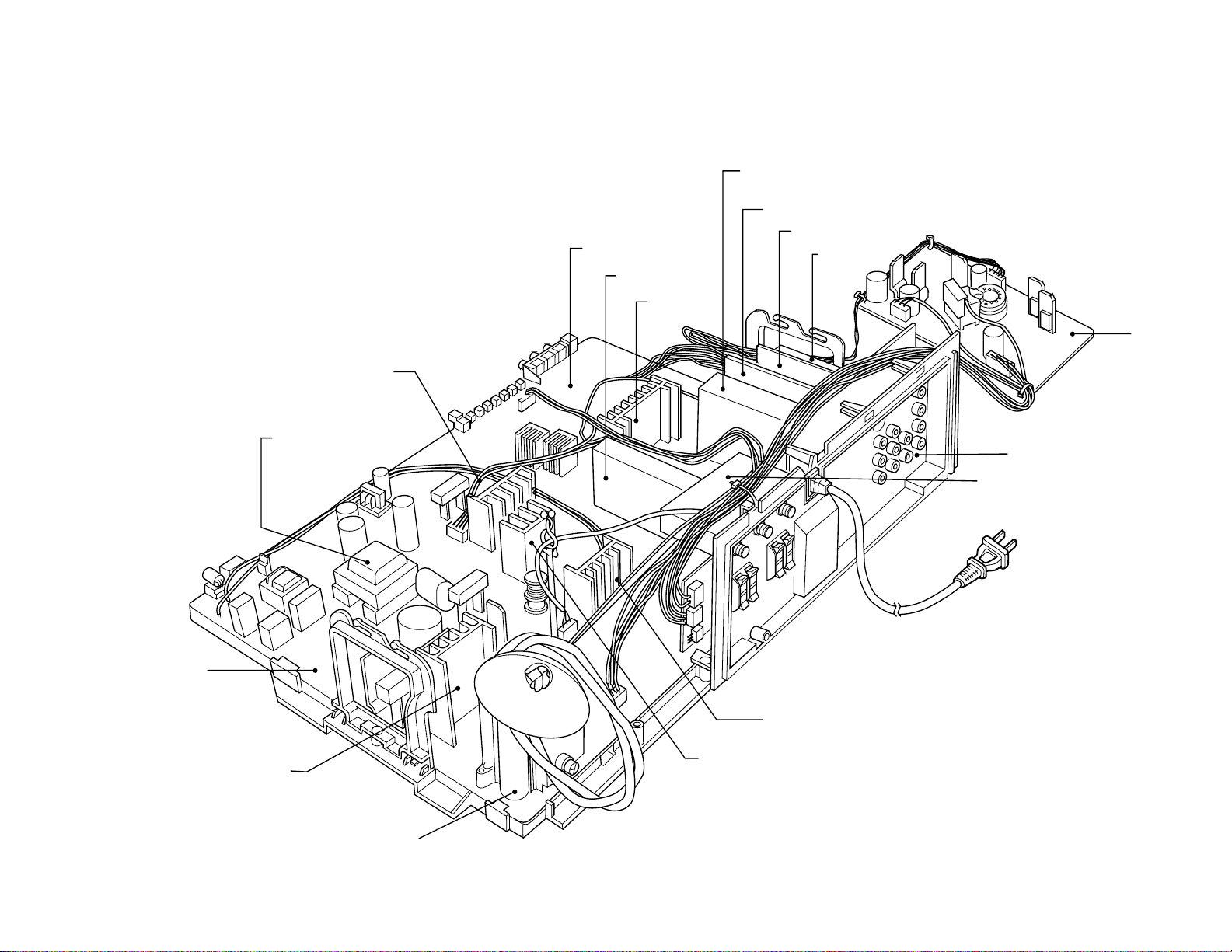
5. CONSTRUCTION OF CHASSIS
REAR AMP circuit
SIGNAL circuit
IF/MTS/A-PRO
module
DPC circuit
CCD circuit
PIP circuit
EDS, RGB SW
circuit
AUDIO OUT
CRT circuit
8
Fig. 1-1
POWER/DEF circuit
CONVERTER trans
A/V circuit
RF SW
V. OUT
DPC circuit
H.OUT
H.OUT trans
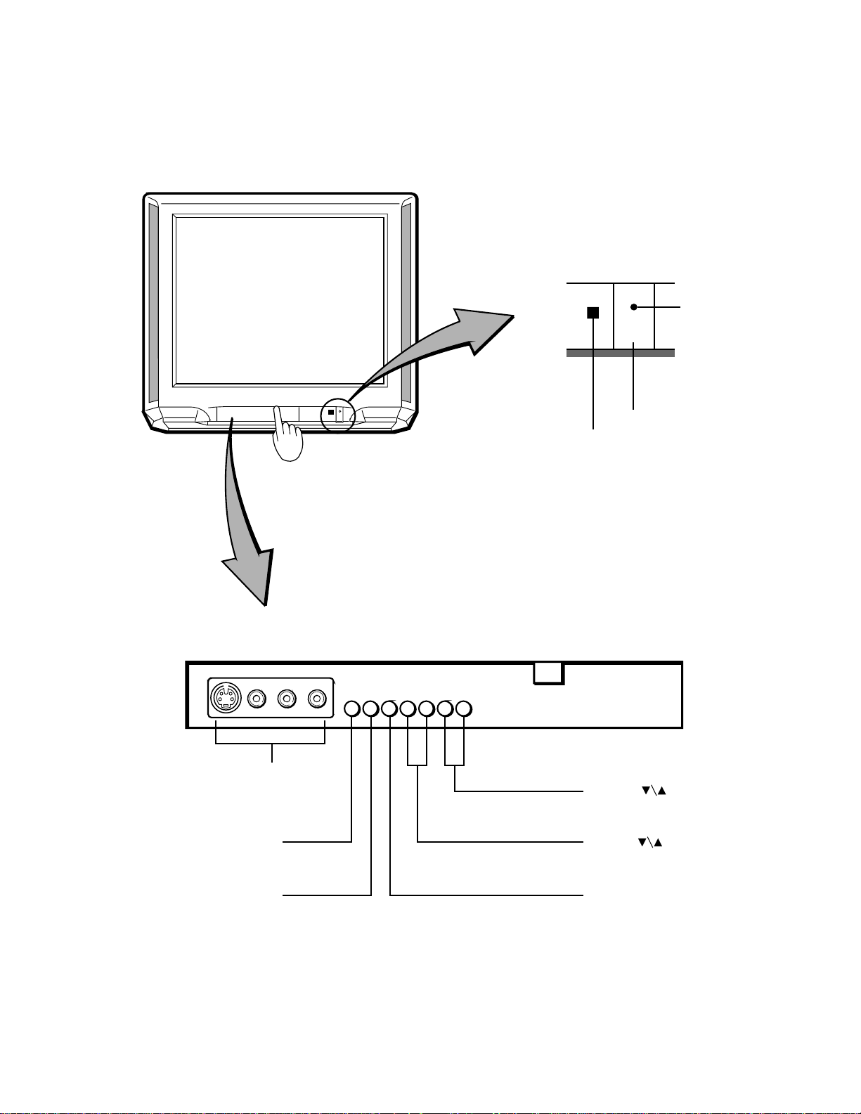
6. LOCATION OF CONTROLS
r
6-1. TV Set
For specific use of each control, consult the corresponding page numbers in brackets.
Front View
POWER indicato
POWER
POWER button
Remote sensor
Behind the door
VIDEO/AUDIO IN
jacks <VIDEO 3>
DEMO button
MENU button
Press to open
the door
CHANNEL
VOLUME
-/+buttons
ANT/VIDEO button
ADV button
buttons
buttons
Fig. 1-2
9
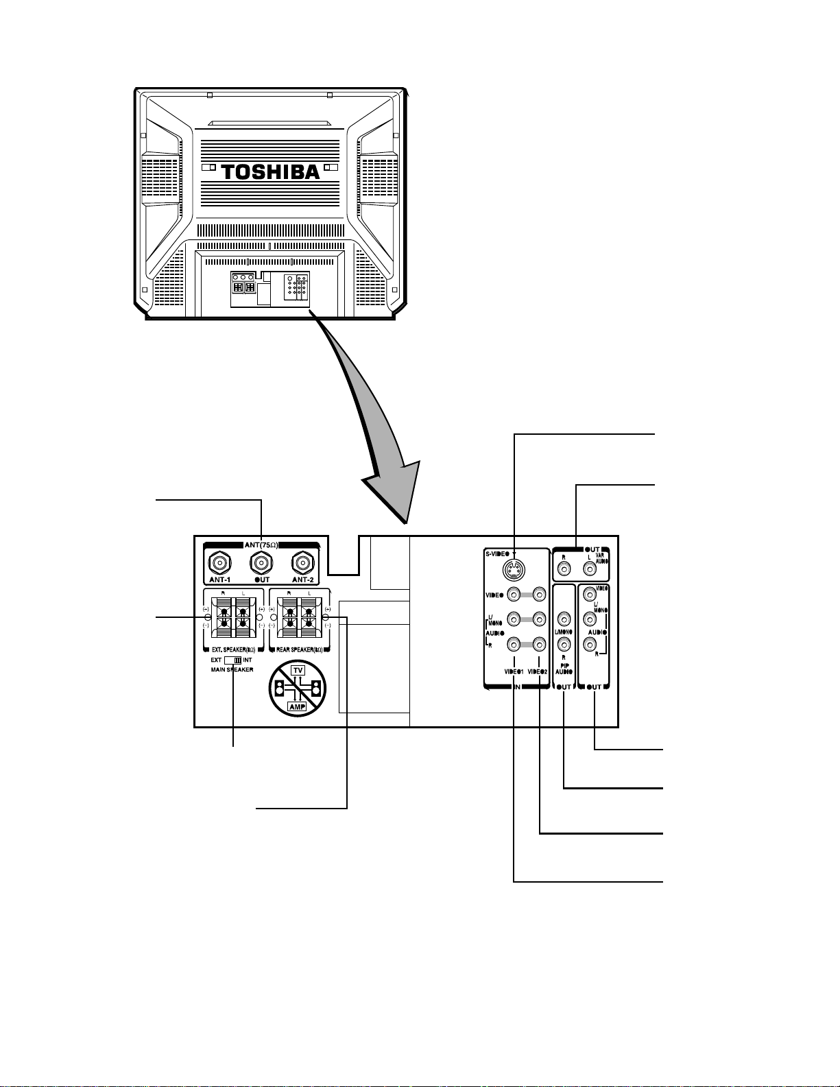
Rear view
t
S-VIDEO IN jack <VIDEO 1>
VARiable AUDIO OUT
ANTenna terminals
EXTernal SPEAKER
erminals
MAIN SPEAKER
switch
REAR SPEAKER
terminals
jacks
VIDEO AUDIO OUT
jacks
PIP AUDIO OUT
jacks
VIDEO/AUDIO IN jacks
<VIDEO 2>
VIDEO/AUDIO IN jacks
<VIDEO 1>
Fig. 1-3
10
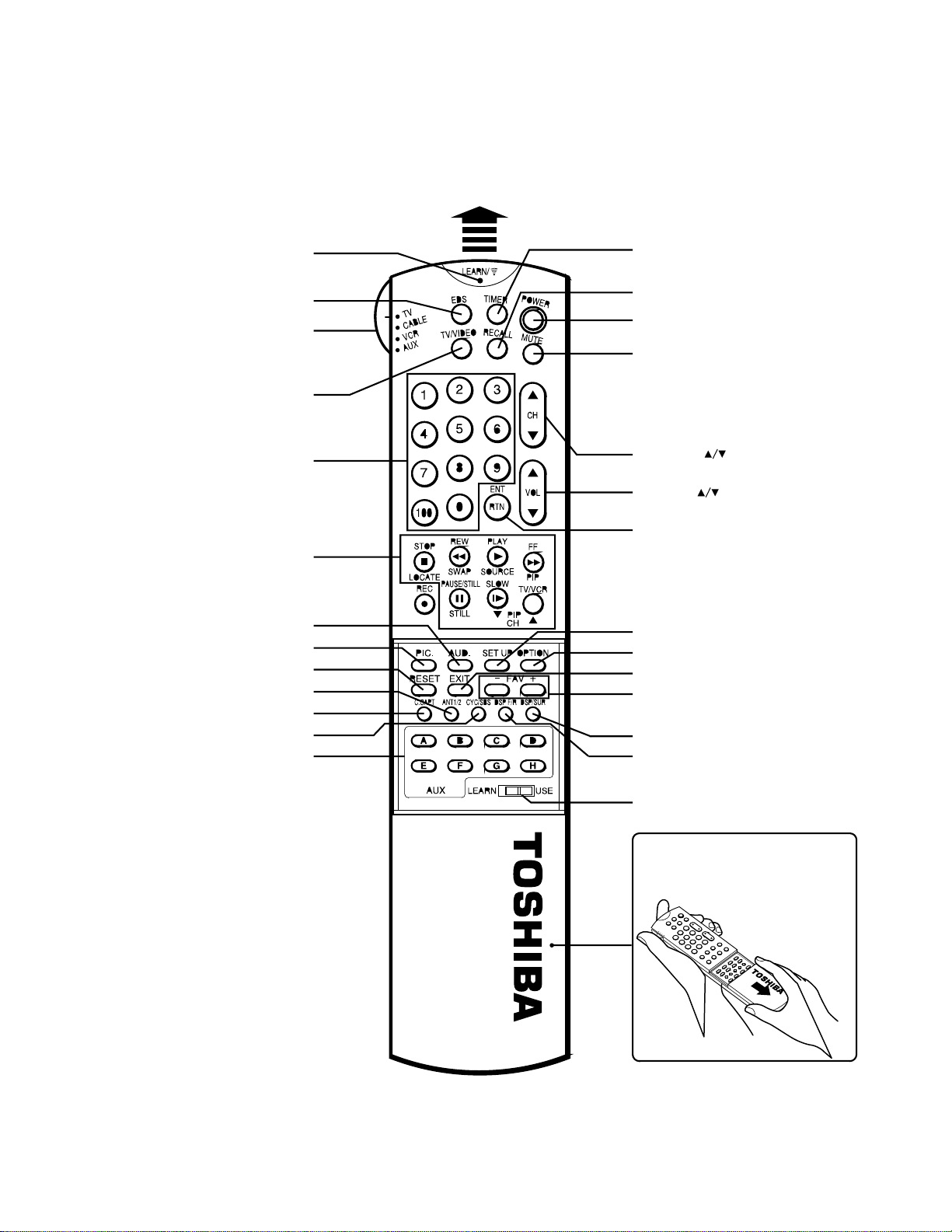
6-2 Location of Controls (Remote Control)
Only the buttons that are used to operate the TV set are described here.
For details on the use of each control, refer to pages in brackets.
Aim at the remote sensor on the TV
Learn/Transmit indicator
EDS button
TV/CABLE/VCR/AUX switch
Set to "TV" to control the TV.
TV/VIDEO
Channel Number buttons
PIP function buttons
AUDio button
PICture button
RESET button
ANT 1/2 button
C.CAPT button
CYS/SBS button
Learning buttons
You can use these eight
buttons only as Learning
function buttons.
They are not affected by
Mode selection (TV/CABLE/
VCR/AUX).
TIMER button
RECALL button
POWER button
MUTE button
CHANNEL buttons
VOLUME buttons
RTN buttons
SET UP button
OPTION button
EXIT button
-\+ buttons
FAV -/+ buttons
DSP/SUR button
DSP F/R button
LEAR/USE switch
To operate buttons inside the cover,
slide the cover down and toward you.
Fig. 1-4
11
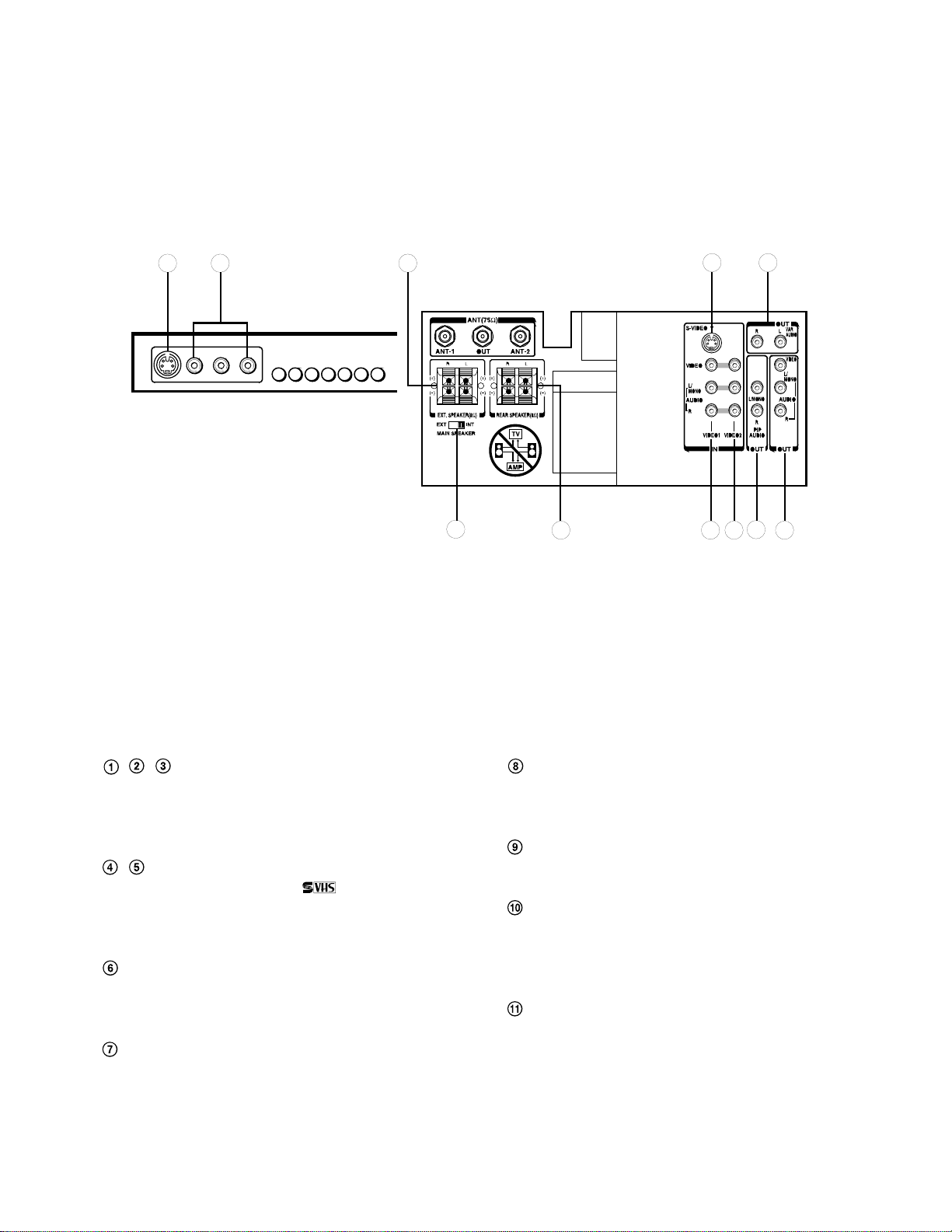
6-3 Monitor Panel
This TV set is equipped with S-VIDEO INPUT jacks,
VIDEO/AUDIO INPUT jacks, VIDEO/AUDIO OUTPUT
jacks, VARIABLE AUDIO OUTPUT jacks, PIP AUDIO
OUTPUT jacks and EXTERNAL SPEAKER terminals for
connecting your desired video/audio equipment.
TV Front
935
TV Rear
10
11 1 2
74
8
6
Fig. 1-5
, , VIDEO 1/VIDEO 2/VIDEO 3 IN Jacks —
provide for direct connection of video devices
(VCR, video disc player, camcorder, etc.) with
video/audio outputs.
, S-VIDEO IN Jacks —provide for direct S-video
connection from an VCR or a video disc
player. The TV's VIDEO 1/3 audio jacks can
also be used to connect the VCR's audio cables.
VIDEO/AUDIO OUT Jacks --- provide fixedlevel audio and video outputs from whatever is
displayed on the screen.
VARIABLE AUDIO OUT Jacks --- feed
volume-controlled stereo audio out from
whatever is displayed on the screen, allows
connection of audio amplifier and lets you adjust
sound level with TV's remote.
12
PIP AUDIO OUT Jacks — provide fixed-level
audio outputs from whatever is displayed on the
PIP window screen.
EXTERNAL SPEAKER Terminals — provide
for direct connection of external speakers.
MAIN SPEAKER Switch — lets you turn off
TV's built-in speakers so that sound will instead
come through speakers connected to
EXTERNAL SPEAKER terminals.
REAR SPEAKER Terminals — provide for
direct connection of the supplied Surround
Speakers.
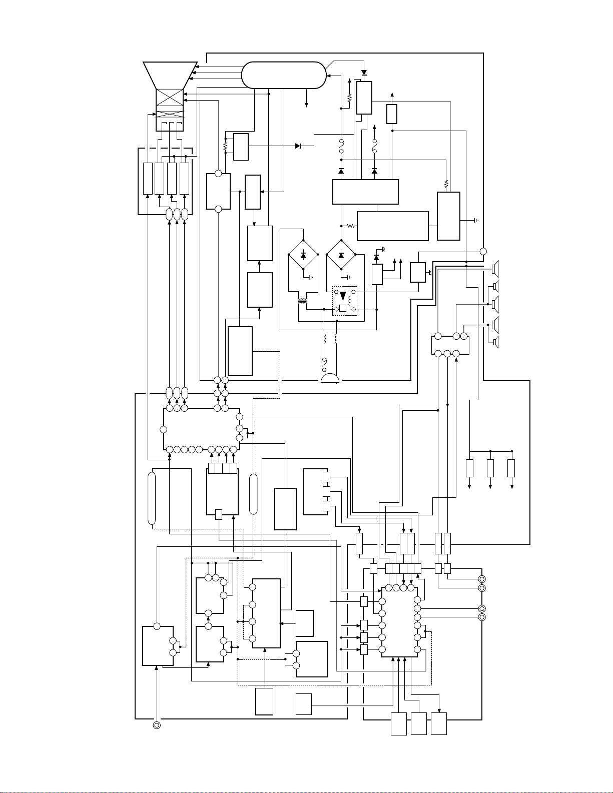
7. CN32D90 BLOCK DIAGRAM
FOCUS
TA1222N
R370
2
301
V OUTPUT
83
35
31
V
YsRG
323534
SCREEN
+27V
TA8427K
84
83
23
H
SDA SCL
CRT
V H
+200V
GREEN OUTPUT
SPEED MOD
CRT DRIVE PCB
RED OUTPUT
144
143
143
144
434241
RGB
12
SYNC
YIO
5838373534
BLUE OUTPUT
145
145
Q501
HIGH VOLTAGE
T461
Q370
2SA933SQ
Q462 DPC
2SC1740S-Q
Q404
H OTUTPUT
Q402
H DRIVE
Q302
TA8859AP
E/W CORRECTION
C
27 28 13
B
33
2SD2253(FA)
2SC1569FA-5
2
Bus line
C
I
-27V
FBT
D840
TB40
TFB
D371
4132AD
4132BD
HEATER
F801 TB01
T862
D801
SR801
5A
D471
33V
+125V
Z801
PROTECTOR
Q420 9V-1
+24.5V
D883 F470 2A
Q801
D885 F883 5A
TRANS
D847
Q840
L78MR05
+12V
CONVERTER
}
PROTECTOR
STBY 5V
RESET
2SC1B15Y
POWER/DEF UNIT
QE06
SW
STROVER HEAT
OVER VOLTAGE
VOLTAGE REG.
Q670
AUDIO OUT
L
R883
Q862
TLP621GR-L
PHOTO-COUPLER
11812
TA8256H
2
1
4
R
W
40
R L W
R L WOOFER
SYNC SIGNAL DET.
SIGNAL UNIT
IF
SCL
43
TUNER
EL922L
HY01(CHILD)
SDA
U/V
145
Ys
S(L)
18
H002
V/SIF/MTS
92
IF
TUNER
H001(MOTHER)
R
G
PIP
MODULE
V
8
S(R)
16
22
6
V
MVUS34S
SCL
EL466L
11 12
SDA
6
B
DC DD
PB5419
C-BUS LINE
2
I
CCD UNIT
V Y C
DG
Q831
Q832
9V-2
Q830
5V-2
5V-3
EDS/C.C
32 31 30 29
SDA SCL STOP SYNC
QA01 MICROCOMPUTER
KEY
CONTROL
V-AV
EH
EA
KEY
6
5
VIDEO
CONTROL
SCL
ICA02
MEMORY
SDA
INPUT 3
24LCO4BI/P
ST24C04CB6
TMP87CS38N-3152
36
38
AB
AA
434530
RLY
V L R V Y
QV01 SIGNAL SW
VIDEO
Y-COMB
EJEIAJ
TA1218N
INPUT 2
C-COMB
32
C
V SDA SCL C
34
2
24 1
42 25
VIDEO
INPUT 1
VAR-L
AI
VIDEO
OUTPUT
VAR-R
AT
L R
VAR
AUDIO
L R
PIP
AUDIO
A/V PCB
Fig. 1-6
13

8. [US, CANADA] SPECIFICATION FOR MODEL's 1995
CHASSIS C C C C C
MODEL Nbr CN27E90 CX32E70 CN32E90 CE35E15 CF35E50
SPECIFICATION HITACHI TDD TDD *TDD *TDD
1 Picture Tube *FST-D/T NF-D/T NF-D/T *FST-D/T FST-D/T
2 Channel Capacity 181ch 181ch 181ch 181ch 181ch
*
3 C. Caption ●●●●●
G
4 MTS with dbx ●●●●●
E
N
5 Bass, Tre, Balance ●●●●●
E
6 Sub-Audio-Program ●●●●●
R
7 Remote band unit *A-Univ (42k) *A-Univ (42k) *Intelig+EZ *Unive (36k) *Unive (36k)
A
8 Picture-in-Picture ● (2TN) ● (2TN) ● (2TN) *● (1TN) ● (1TN)
L
9 LED Indicators (RED) ● (Power) ● (Power) ● (Power) *● (Power) ● (Power)
10 Local Keys 8key 8key 8key 8key 8key
11 Dolby Surround — — ● ——
12 Dig-Sound Processor — — ● (DSP4ch) — —
*
13 Front Surround ●●—●●
S
14 Cyclone ABX ● — ● ——
O
15 Sub-Bass-System — ● ———
U
16 Audio Output *10Wx2 & 13W 10Wx2 10Wx2 & 10Wx2 10Wx2
N
D
17 Speaker Size & Nbr *80x120x2 70x130x2 80x120x2 70x130x2 70x30x2
18 Comb Filter *● (GLS) ● (CCD) ● (CCD) ● (CCD) ● (GLS)
*
19 Dy-Quadruple Focus — — — — —
P
20 Scan Velocity Modu ●●●●●
I
21 Vert Contour Corre ●●●●●
C
22 Black Level Expand ●●●●●
T
23 Flesh Tone Correct *●●●●●
U
R
24 Dynamic Noise Reduc *●●●●●
E
25 Picture Preference ●●●●●
26 Horiz Resolution 650 700 700 800 800
27 Parental-Ch Lock ●●●●●
*
28 Channel Label (32ch) ●●●●●
O
29 3-Language Display ●●●●●
T
30 Clock/Off-Timer *●/●●/●●/●●/●●/●
H
31 Favorite Channel *● *● *● *● *●
E
R
32 Extended-Data-Servi *● *● *● *● *●
33 Star-Sight-decoder — — — — —
34 S-Video In-Term ● (1+1) ● (1+1) ● (1+1) ● (1) ● (1)
35 Audio, Video-In/Out 1+2/— 1+2/1 1+2/1 *3/1 3/1
*
36 Front AV Jack *●●●——
T
E
37 Variable Audio Out ●●●●●
R
38 2-RF Input ●●●——
M
39 Ext Speaker Term ●●●●●
S
40 PIP Audio Out Jack — *— *● ——
41 Center-Ch-Aud-Input — *● *— — —
42 Speaker-Box -- — ● SS-SR94 — —
*
AC
43 Others — — — — —
*Cabinet NEW CX32D70 CN32D90 *CE35D10 CF35D50
PARTS SUPPLY (ISO) — — — — —
CRT
13W & 5Wx2
& 100R (Hon) 100R & REAR
DERIV
14

CHASSIS C C C C C
MODEL Nbr CX35E60 CX35E70 CX35E81 CN35E90 CN35E95
SPECIFICATION TDD TDD TDD TDD TDD
1 Picture Tube FST-D/T NF-D/T NF-D/T NF-D/T NF-D/T
2 Channel Capacity 181ch 181ch 181ch 181ch 181ch
*
3 C. Caption ●●●●●
G
4 MTS with dbx ●●●●●
E
N
5 Bass, Tre, Balance ●●●●●
E
6 Sub-Audio-Program ●●●●*●
R
7 Remote band unit *A-Univ (42k) *A-Univ (42k) *A-Univ (42k) *Intelig+EZ *Intelig+EZ
A
8 Picture-in-Picture ● (2TN) ● (2TN) ● (2TN) ● (2TN) ● (2TN)
L
9 LED Indicators (RED) ● (Power) ● (Power) ● (Power) ● (Power) ● (Power)
10 Local Keys 8key 8key 8key *8key *8key
11 Dolby Surround — — — ●●
12 Dig-Sound Processor — — — ● (DSP4ch) ● (DSP4ch)
*
13 Front Surround ●●●——
S
14 Cyclone ABX — — — ●●
O
15 Sub-Bass-System ●●●——
U
16 Audio Output 10Wx2 10Wx2 10Wx2 10Wx2 10Wx2
N
D
17 Speaker Size & Nbr 70x130x2 70x130x2 70x130x2 80x120x2 & 80x120x2 &
18 Comb Filter ● (DIG) ● (DIG) ● (DIG) ● (DIG) ● (DIG)
*
19 Dy-Quadruple Focus ●●●●●
P
20 Scan Velocity Modu ●●●●●
I
21 Vert Contour Corre ●●●●●
C
22 Black Level Expand ●●●●●
T
23 Flesh Tone Correct ●●●●●
U
R
24 Dynamic Noise Reduc ●●●●●
E
25 Picture Preference ●●●●●
26 Horiz Resolution 800 800 800 800 800
27 Parental-Ch Lock ●●●●●
*
28 Channel Label (32ch) ●●●●●
O
29 3-Language Display ●●●●●
T
30 Clock/Off-Timer ●/●●/●●/●●/●●/●
H
31 Favorite Channel *● *● *● *● *●
E
R
32 Extended-Data-Servi *● *● *● *● *●
33 Star-Sight-decoder — — — — —
34 S-Video In-Term ● (1+1) ● (1+1) ● (1+1) ● (1+1) ● (1+1)
35 Audio, Video-In/Out 1+2/1 1+2/1 1+2/1 1+2/1 1+2/1
*
36 Front AV Jack ●●●●●
T
E
37 Variable Audio Out ●●●●●
R
38 2-RF Input ●●●●●
M
39 Ext Speaker Term ●●●●●
S
40 PIP Audio Out Jack — *— *— *● *●
41 Center-Ch-Aud-Input — *● *● *— *—
42 Speaker-Box — — — ● SS-SR94 ● SS-SR94
*
AC
43 Others — *VCR-Storate — *VCR-Stora
*Cabinet C35D60 CX35D70 NEW (DAX) CN35D90 NEW (BLK)
PARTS SUPPLY (ISO) — — — — —
CRT
CONSOLE CINEMA
& 13W, 5Wx2 & 13W, 5Wx2
*100R, REAR *120R, REAR
15

SECTION II
TUNER, IF/MTS/S.PRO MODULE
16
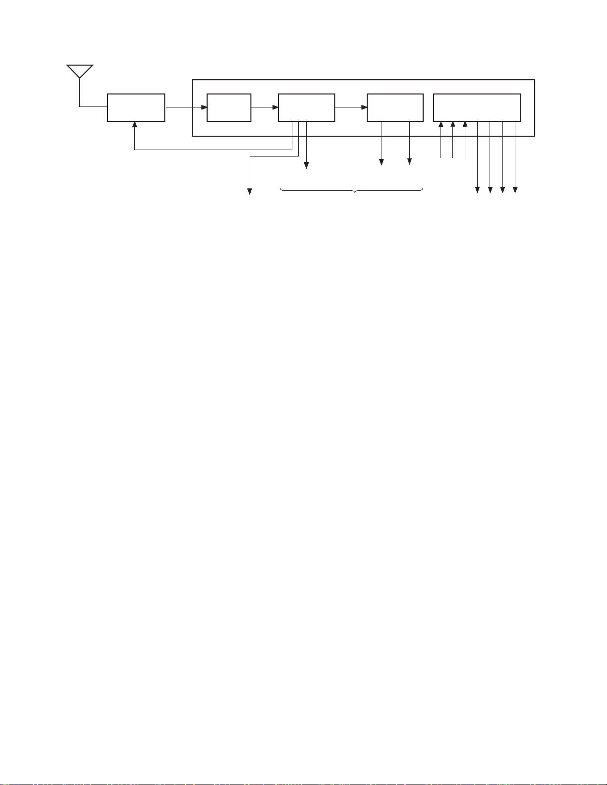
1. CIRCUIT BLOCK
T
EL466L
Tuner
RF AGC
1-1. Outline
IF/MTS/S.PRO Module MVUS34S
SAW
Filter
AFT output
VIF/SIF
Circuit
TP12
Video output
Fig. 2-1 Block diagram
SIF
output
To A/V switch circuit
Multiplex
TV
R-OUTTVL-OUT
Sound
Circuit
C-IN
S.PRO Circuit
R-IN L-IN
R-OUT
L-OUT
(L+R)
-OUT
C-OU
(1) RF signals sent from an antenna are converted into
intermediate frequency band signals (video: 45.75 MHz,
audio: 41.25 MHz) in the tuner. (Hereafter, these signals
are called IF signals.)
(2) The IF signals are band-limited in passing through a
SAW filter.
(3) The IF signals band-limited are detected in the VIF
circuit to develop video and AFT signals.
(4) The band-limited IF signals are detected in the SIF
circuit and the detected output is demodulated by the
audio multiplexer, developing R and L channel outputs.
These outputs are fed to the A/V switch circuit.
(5) A sound processor (S.PRO.) is provided.
1-2. Major Features
(1) The VIF/SIF circuit is fabricated into a small module by
using chip parts considerably.
(2) As the tuner, EL466L that which contains an integrated
PLL circuit is employed.
(3) Wide band double SAW filter F1802R used.
(4) FS (frequency synthesizer) type channel selection system
employed.
(5) VIF/SIF circuit uses PLL sync detection system to
improve performances shown below:
• Telop buzz in video over modulation
• DP, DG characteristics (video high-fidelity
reproduction)
• Cross color characteristic (coloring phenomenon at
color less high frequency signal objects)
(6) HIC SBX1637A-22 is used in the audio multiplexer
circuit to minimize the size with increased performance.
(7) As a sound control processor, TA1217N is used. I2C-
bus data control the DAC inside the IC to perform
switching of the audio multiplexer modes.
17
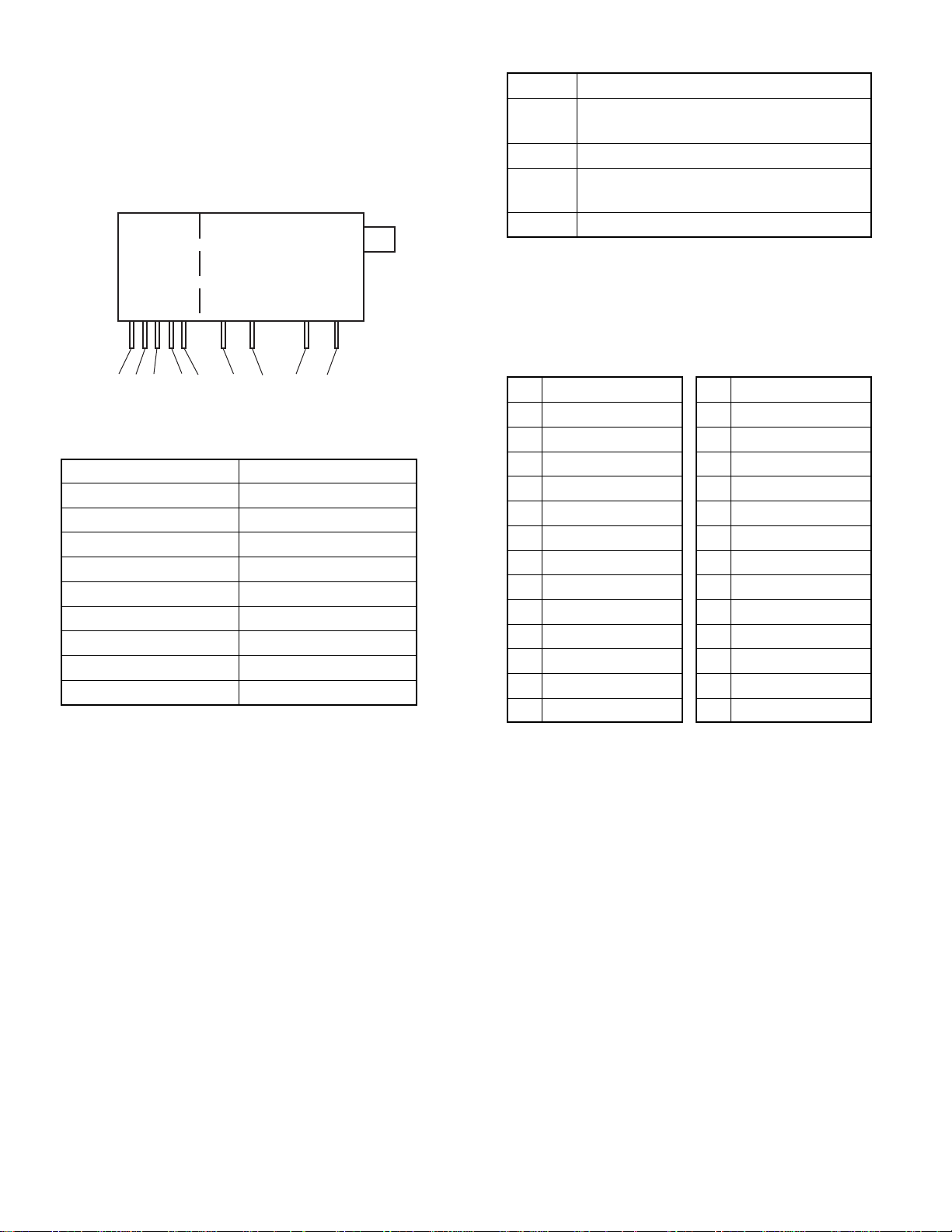
2. TUNER
2-1. Outline
(1) Type name: EL466L
(2) Applicable 181CH
(3) I2C-bus version
(4) PLL-integrated
2-2-2. Terminals (Tuner section)
Name Function
IF OUT IF outputs (P=45.75 MHz, C=42.17 MHz,
S=41.25 MHz)
BM Tuner power supply (9V)
RF AGC Gain control terminal to obtain constant
IF output
VT Control voltage to select channels
PLL Selection
EL466L
Tuner Section
1 2 3 4 5 6 7 8 9
Terminal No. Name
1 32V
25V
3 S-CLOCK
4 S-DATA
5 ADDRESS
6 IF OUT
7 BM (9V)
8 RF AGC
9VT
Fig. 2-2 Tuner terminal layout
2-2-3. Tuner VT Voltage (unit: V)
(1) VHF (2) UHF
CH VT voltage (TYP)
2 1.4
6 6.4
A-2 12.8
B 20.0
C 1.4
I 3.5
10 5.6
J 7.6
N 9.7
R 11.8
W 14.2
FF 17.9
LL 24.2
CH VT voltage (TYP)
MM 1.1
QQ 2.2
WW 4.0
14 5.8
20 7.8
26 9.2
32 10.8
38 12.5
44 13.9
50 15.0
56 17.2
62 19.4
69 23.6
* VT voltage not indicated for a channel falls between
those values for channels just upper and lower the channel.
2-2. Operation of the Tuner
2-2-1. Receiver Channels
VHF 2~13CH
UHF 14~69CH 181CH in total
CATV A-6~, J~W, AA~BBB, 65~92, 100~127CH
18
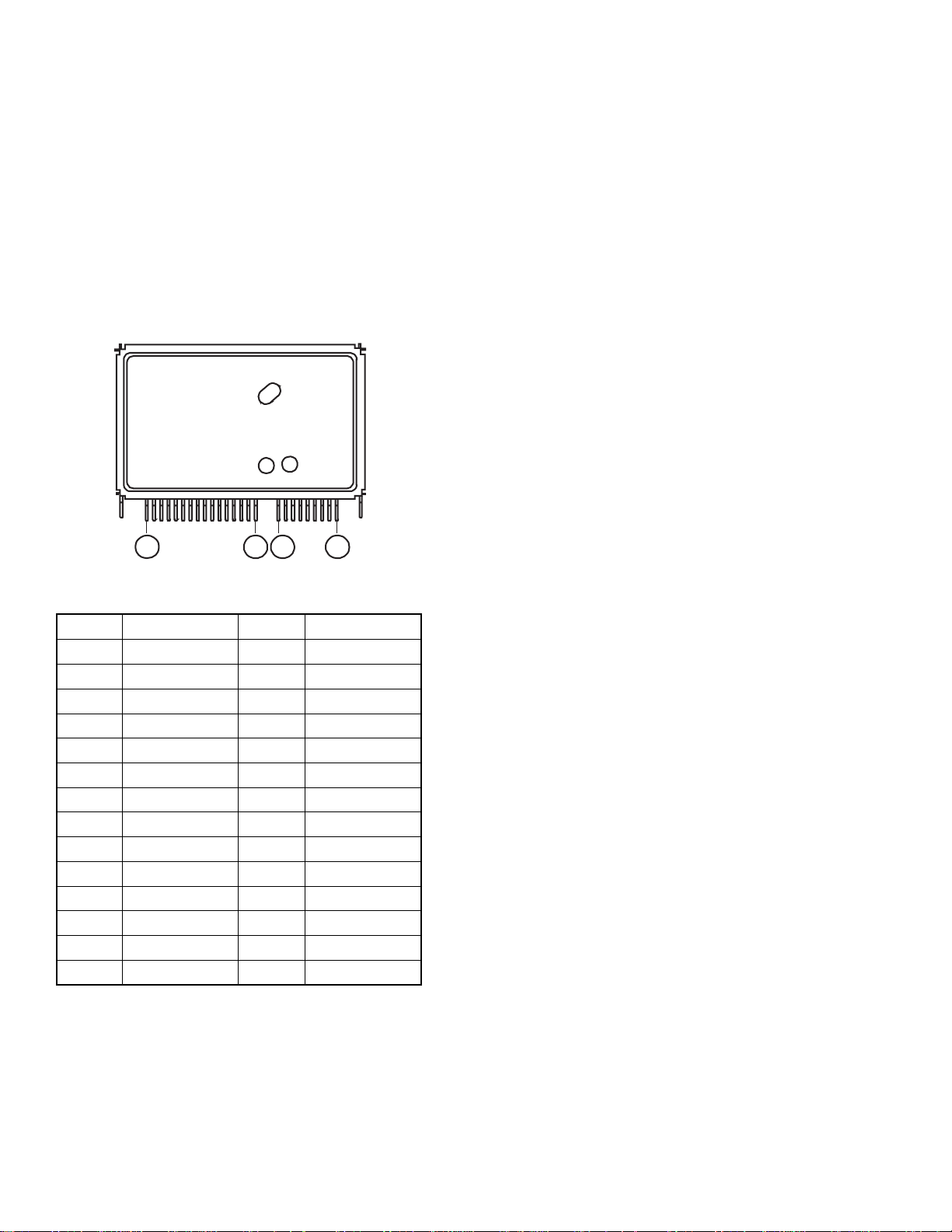
3. IF/MTS/S.PRO MODULE
The IF/MTS/S.PRO module (MVUS34S) limits bandwidth
of IF signals and detects video and audio signals. The module
consists of IF amplifiers, SAW (surface acoustic wave)
filter, and PIF IC. The SAW filter has a wideband response
to improve picture quality and audio buzz characteristic and,
develops separate outputs of video and audio signals. The
PIF IC employs a PLL complete sync detection + audio split
carrier system.
3-1-2 Video PIF Circuit
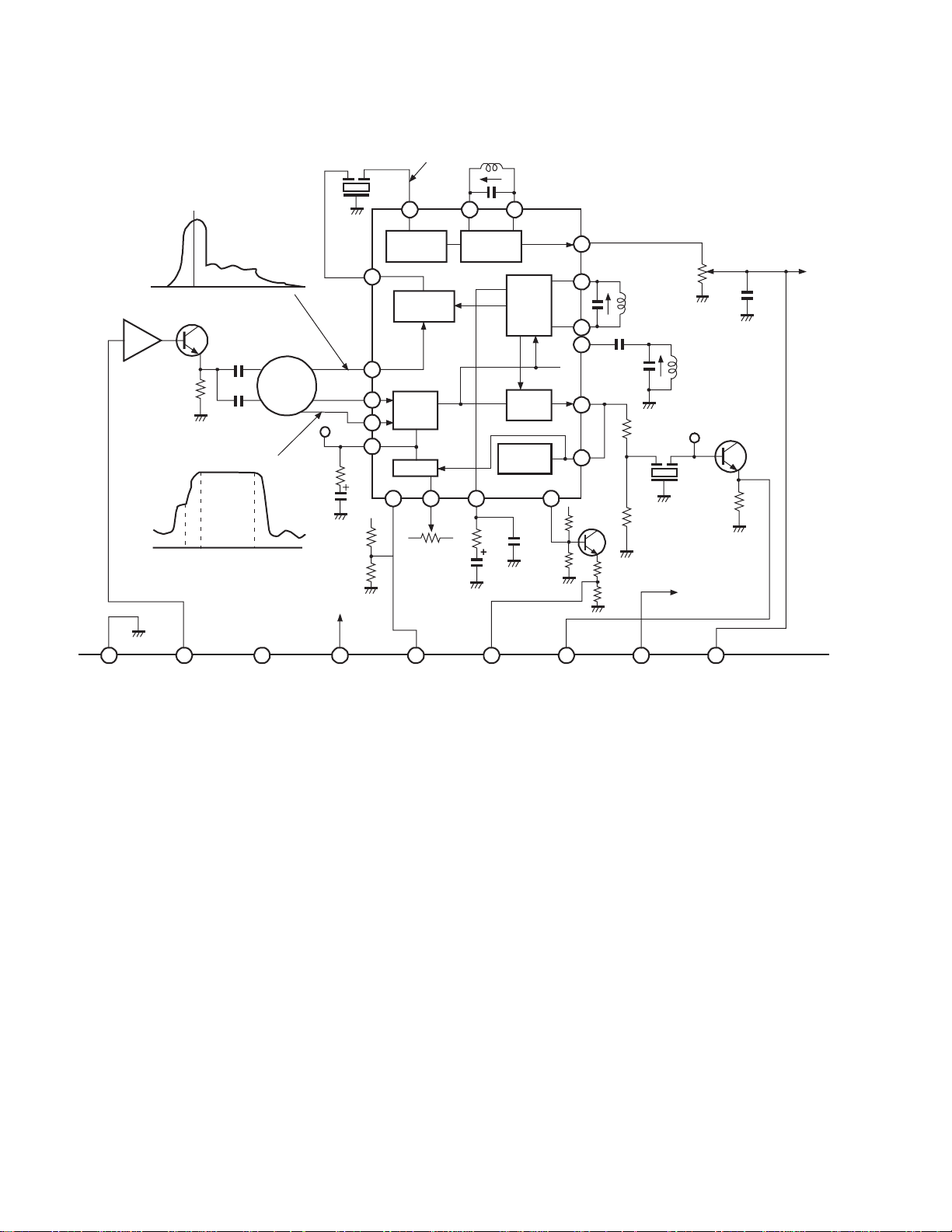
A PIF detector switching carrier is oscillating at a frequency
adjusted to 45.75 MHz with L051 (VCO CW coil) under no
RF signal input. When an RF signal enters, an IF video
carrier is fed to APC section from IF AMP inside the IC, and
the detector switching carrier is adjusted by the APC, VCO,
etc. in the PLL circuit so that its frequency and phase are
matched to those of the IF video carrier to perform precise
sync detection. Thus processed video output is developed at
pin 21.
3-1. IF/MTS/S.PRO Module (MVUS34S)
3-1-1. Module Terminal Layout
91
27
12
Pin No. Name Pin No. Name
1 GND 15 DAC-OUT2
2 IF-IN 16 R-IN
3 NC 17 C-IN
4 +9V 18 L-IN
5 RF AGC 19 GND
6 AFC 20 SCL
7 VIDEO OUT 21 SDA
8 ADR SW 22 W-OUT
9 MPX OUT 23 C-OUT
10 --- 24 L-OUT
11 --- 25 GND
12 TV R-OUT 26 R-OUT
13 DAC-OUT1 27 +9V
14 TV L-OUT
PLL lock speed is automatically controlled by adding the
video signal at pin 21 to pin 1. That is, since the video signal
is not output at operations of power on, CH switching, etc.,
the APC filter between pin 16 and GND consists of C022 and
C053, and R018, and the filter effect decreases, thus increasing
PLL lock speed.
Next, when a video out exists, the internal resistance is shortcircuited and the APC filter consists of C022 and C053,
internal resistance, and R018. As a result, the filter effect
increases and the PLL lock speed decreases. Consequently,
under normal signal reception, phase of the detector switching
carrier is locked in a stable condition if an IF video carrier is
lost for a short time due to over modulation, etc. By combining
such a PLL complete sync detection system and a wideband
SAW filter shown in Fig. 2-4, a wideband (4.2 MHz) video
detection output with less beat interference will be obtained.
3-1-3. Audio PIF Circuit
The IF signal fed through Q003 (Fig. 2-4) enters an audio
section of the SAW filter (Z001) which has an IF bandwidth
for dedicated audio signals, and only the audio signal of
41.25 MHz is fed to pin 7. The signal is sync-detected with
the detection carrier completely synchronized with the IF
video carrier and pin 14 develops a 4.5 MHz SIF signal. By
using the PLL split carrier system just stated, audio signals
with less buzz by the video signal will be reproduced. The 4.5
MHz SIF enters pin 15 through a 4.5 MHz filter, Z003 and
pin 9 develops a FM-detected audio signal.
Fig. 2-3 IF/MTS/S.PRO module terminal layout
19
SIF BANDWIDTH
M
D
Z003
4.5MHz SIF SIGNAL
15
11 12
FM DET. COIL
L053
9
17.
18
23
21
1
R151
L051
VCO
CW COIL
L502
AFT COIL
TP12
R021
Z002
R022
TO SOUN
MPX IC
C106
Q004
Q002
Q003
IF AMP
GAIN – 14dB
-15dB
S C P
41.25M 45.75M
S
Z001
SAW
FILTER
F1802R
-6dB
SIF LIMIT FM DET.
14.
SIF DET
7
5
IF
AMP
4
22
AGC
2
13 16 20
RF AGC
R051
R018
C053
APC
VCD
VIDEO
DET.
LOCK
CONTROL
C022
VIDEO IF BANDWIDTH
1 2
3
4 5 6
7
8
9
GND IF-IN N.C +B(9V) RF AGC AFC VIDEO OUT ADR SW
Fig. 2-4 IF/MTS/S. PRO circuit diagram
20
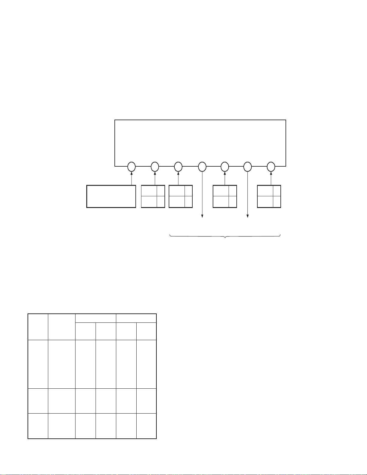
3-1-4. Audio Multiplex Demodulation Circuit
The sound multiplex composite signal FM-detected in the
PIF circuit enters pin 12 of HIC (hybrid IC) in passing
through the separation adjustment VR RV2 and amplified.
After the amplification, the signal is split into two: one enters
a de-emphasis circuit, and only the main signal with the LR signal and a SAP signal removed enters the matrix circuit.
At the same time, the other passes through various filters and
trap circuits, and the L-R signal is AM-demodulated, and the
SAP is FM-demodulated.
MVUS32S
Then, both are fed to the matrix circuit. At the same time,
each of the stereo pilot signal fH and the SAP pilot signal 5fH
is also demodulated to obtain an identification voltage. With
the identification voltage thus obtained and the user control
voltage are used to control the matrix.
The audio signals obtained by demodulating the sound
multiplex signal develop at pin 10 and 11 of HIC and develop
the terminals of 12 and 14 of the module.
MPX
Out
9
Monitor the input
pin for multiplex
sound IC
10
Stereo 0V
Other 0V
Fig. 2-5 Block diagram of MVUS32S
Table 2-1 Matrix for broadcasting conditions and
reception mode
Output OSD display
Broad- Switching
casted mode
12 pin 14 pin
(R) (L)
Stereo SAP
Stereo STE R L O X
SAP R L O X
MONO L+R L+R O X
Mono STE L+R L+R X X
SAP L+R L+R X X
MONO L+R L+R X X
Stereo STE R L O O
+ SAP SAP SAP O O
SAP MONO L+R L+R O O
Mono STE L+R L+R X O
+ SAP SAP SAP X O
SAP MONO L+R L+R X O
DAC-out1 DAC-out2
TV TV
(SURR OFF)
R-Out
11
SAP 0V
Other 0V
TV waveform detection
12 13 14
OFF 0V
ON 9V
Not used for
CN32E90.
output (R)
To AV select circuit
Note:
Of the mode selection voltages, switching voltages for STE,
SAP, MONO do not output outside the module.
They are used inside the module to control the BUS.
L-Out
TV waveform detection
output (L)
(RFSW)
14
RF1 0V
RF1 9V
21
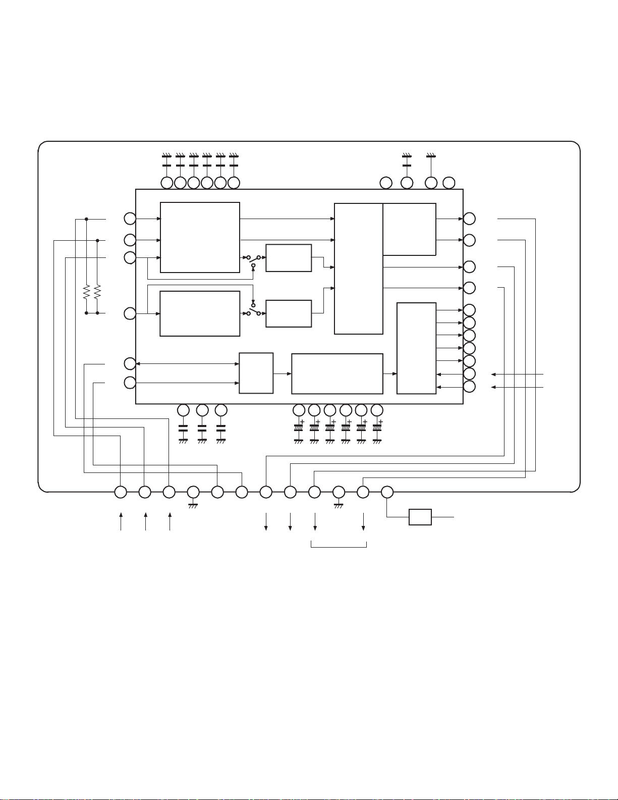
3-1-5. A.PRO Section (Audio Processor)
The S.PRO section has following functions.
(1) Woofer processing (L+R output)
(2) High band, low band, balance control
(3) Sound volume control, cyclone level control
(4) Cyclone ON/OFF
TA1217N
All these processing are carried out according to the BUS
signals sent from a microcomputer.
Fig. 2-6 shows a block diagram of the A.PRO IC.
Lin
Rin
Cin
Win
SDA
SGL
1272922 32
30
34
2
3
20
21
TONE CONTROL
LPF
4
33
Center
LEVEL
Woofer
LEVEL
2
I C
56 73124
D/A
CONV
VOLUME
23 22 19
30 9 8 28
BALANCE
I/O
26
Lout
Rout
25
Cout
18
Wout
10
17
16
15
14
13
12
11
SAP det.
STE det.
16
R-in C-in L-in
From From From
A/V Dolby A/V
18 19 20 21 22
17
24
23
SCL SDA W-out O-out L-out R-out
Q670 Q640 Q670 Q670
Via QS101
26 27
25
Fig. 2-6 A.PRO block diagram
22
9V
4. PIP TUNER
Lable
Name
Lot No.
1
15
TUNER
SECTION
RF AGC
SAW
FILTER
AFT
OUTPUT
VIF/SIF
CIRCUIT
VIDEO
OUTPUT
AUDIO
OUTPUT
Fig. 2-7
4-1. Outline
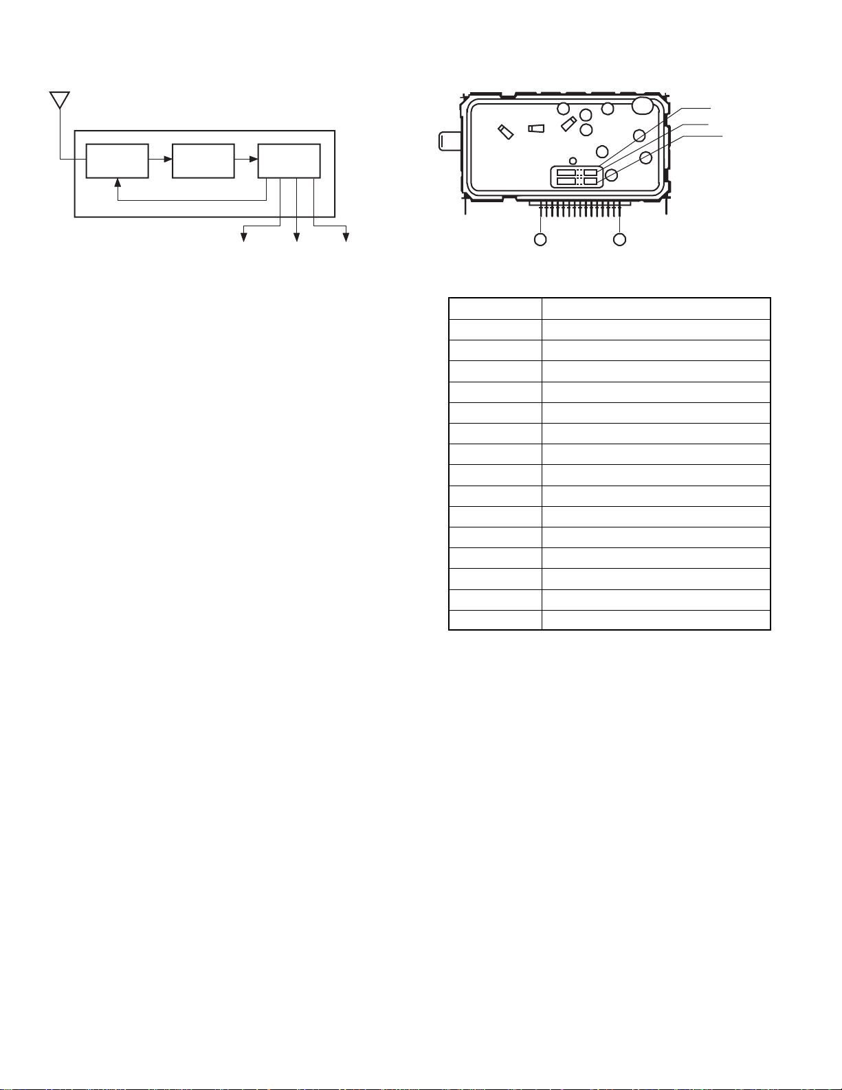
The PIP tuner (EL922L) consists of a tuner and an IF block
integrated into one unit. The tuner receives RF signals
induced on an antenna and develops an AFT output, video
output, and audio output.
The tuner has receive channels of 181 as in the tuner for the
main screen and it is also controlled through the I2C-bus.
As the IC for the IF, a PLL complete sync detection plus
audio inter carrier system are employed.
Terminal No. Name
1NC
2 32V
3 S-CLOCK
4 S-DATA
5NC
6 ADDRESS
75V
8 RF AGC
99V
10 AUDIO
11 GND
12 AFT
13 NC
14 GND
15 VIDEO
Fig. 2-8 Tuner terminal layout
23

SECTION III
CHANNEL SELECTION CIRCUIT
24

1. OUTLINE OF CHANNEL SELECTION
CIRCUIT SYSTEM
The channel selection circuit in the N5SS chassis employs
a bus system which performs a central control by connecting
a channel selection microcomputer to a control IC in each
circuit block through control lines called a bus. In the bus
system which controls each IC, the I2C bus system (two line
bus system) developed by Philips Co. Ltd. in the Netherlands
has been employed.
The ICs controlled by the I2C bus system are : IC for audio
signal processing (QN06), IC for V/C/D signal processing
(Q501), IC for A/V switching (QV01), IC for non volatile
memory (QA02), Main and sub U/V tuners (H001, HY01),
IC for deflection distortion correction (Q302), IC for PIP
signal processing (QY04), IC for DSP (QM01), IC for
closed caption control (Q701).
Differences from N4SS chassis are as follows;
1. On-screen function inside microcomputer is used.
Separate IC is not used for on-screen.
2. The microcomputer does not have the closed caption
function, but controls separate IC for closed caption.
3. The system uses two channels of I2C bus. One is only
for non-volatile memory.
2. OPERATION OF CHANNEL
SELECTION CIRCUIT
Toshiba made 8 bit microcomputer TLCS-870 series for TV
receiver, TMP87CS38N-3152 is employed for QA01.
With this microcomputer, each IC and circuit shown below
are controlled.
(1) CONTROL OF AUDIO SIGNAL PROCESS IC (QN06
Toshiba TA1217N)
• Adjustments for volume, treble, bass and balance
• Selection between surround mode and DSP mode,
and level adjustment
• Level adjustment of BAZOOKA system
• Audio muting during channel selection or no signal
reception.
(2) CONTROL OF VIDEO/CHROMA/DEF SIGNAL
PROCESS IC (Q501 Toshiba TA1222N)
• Adjustments for uni-color, brightness, tint, color
gain, sharpness and PIP uni-color
• Setting of adjustment memory values for subbrightness, sub-color and sub-tint, etc.
• Setting of memory values for video parameters
such as white balance (RGB cutoff, GB drive) and
g correction, etc.
• Setting of video parameters of video modes
(Standard, Movie, Memory)
(3) CONTROL OF A/V SWITCH IC (QV01 Toshiba
TA1219N)
• Preforms source switching for main screen and
sub screen
• Performs source switching for TV and three video
inputs
(4) CONTROL OF NON-VOLATILE MEMORY IC
(QA02 Microchip 24LC04BI/P)
• Memorizes data for video and audio signal
adjustment values, volume and woofer adjustment
values, external input status, etc.
• Memorizes adjustment data for white balance
(RGB cutoff, GB drive), sub-brightness, sub color,
sub tint, etc.
• Memorizes deflection distortion correction value
data adjusted for each unit.
(5) CONTROL OF U/V TUNER UNIT (H001 Matsushita
EL466L, HY01 Toshiba EL922L)
• A desired channel can be tuned by transferring a
channel selection frequency data (divided ratio
data) to the I2C bus type frequency synthesizer
equipped in the tuner, and by setting a band switch
data which selects the UHF or VHF band.
(6) CONTROL OF DEFLECTION DISTORTION
CORRECTION IC (Q302 Toshiba TA8859P)
• Sets adjustment memory value for vertical
amplitude, linearity, horizontal amplitude,
parabola, corner, trapezoid distortion.
(7) CONTROL OF PIP SIGNAL PROCESS IC (QY04
Toshiba TC9083F)
• Controls ON/OFF and position shift of PIP.
(8) CONTROL OF DIGITAL SOUND PROCESSOR IC
(QM04 Yamaha YSS238-D)
• Performs mode switching of DSP.
(9) CONTROL OF CLOSED CAPTION/EDS (QM01
Motorola XC144144P)
• Controls Closed Caption/EDS.
25
3. MICROCOMPUTER
SDA
SCL
1 - 7
8
9 1 - 7
8
9
1 - 7
8
9
START
CONDITION
STOP
CONDITION
ADDRESS
R/W
Ack DATA
Ack
DATA Ack
Approx.180
m
S
Some device may have no data,
or may have data with several
bytes continuing.
Microcomputer TMP87CS38N-3152 has 60k byte of ROM
capacity and equipped with OSD function inside.
The specification is as follow.
• Type name : TMP87CS38N-3152
• ROM : 60k byte
• RAM : 2k byte
• Processing speed : 0.5m s (at 8MHz with Shortest
command)
• Package : 42 pin shrink DIP
• I2C-BUS : two channels
• PWM : 14 bit x 1, 7 bit x 9
• ADC : 8 bit x 6 (Successive comparison system,
Conversion time 20ms)
• OSD
Character kinds : 256
Character display : 24 characters x 12 lines
Character dot : 14 x 18 dots
Character size : 3 kinds (Selected by line)
Character color : 8 colors (Selected by character)
Display position : Horizontal 128 steps, Vertical
256 steps
This microcomputer performs functions of AD converter,
reception of U/V TV and OSD display in one chip.
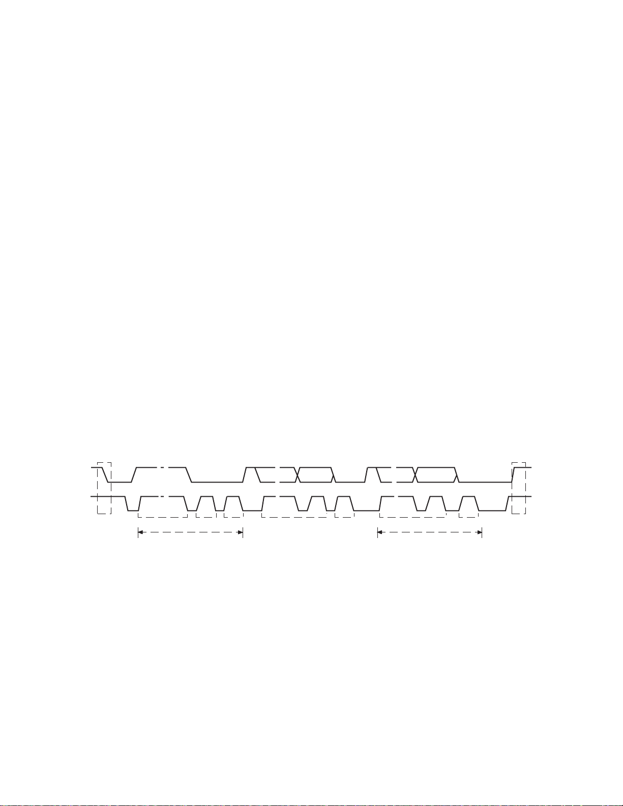
IIC device controls through I2C bus. (Timing chart : See fig.
3-1)
• LED uses big current port for output only.
• For clock oscillation, 8MHz ceramic oscillator is used.
• I2C has two channels. One is for EPROM only.
• Self diagnosis function which utilizes ACK function of
I2C is equipped
• Function indication is added to service mode.
• Remote control operation is equipped, and the control
by set no touch is possible. (Bus connector in the
conventional bus chassis is deleted.)
• Substantial self diagnosis function
(1) B/W composite video signal generating function
(micom inside, green crossbar added)
(2) Generating function of audio signal equivalent
to 1kHz (micom inside)
(3) Detecting function of power protection circuit
operation
(4) Detecting function of abnormality in IIC bus
line
(5) Functions of LED blink indication and OSD
indication
(6) Block diagnosis function which uses new VCD
and AV SW
Fig. 3-1
26
4. MICROCOMPUTER TERMINAL FUNCTION
TMP87CS38N3152 (QA01)
GND
1
GND
VDD
42
VDD
IIC
-BUS
BAL
REM OUT
MUTE
SP MUTE
NC
POWER
LED
NC
NC
SCL0
SDA0
SYNC VCD
NC
AFT2
AFT1
KEY-A
KEY-B
SGV
SGA
GND
10
11
12
13
14
15
16
17
18
19
20
21
2
I
P40 (PWM0)
3
O
P41 (PWM1)
4
O
P42 (PWM2)
5
O
P43 (PWM3)
6
O
P44 (PWM4)
7
O
P45 (PWM5)
8
O
P46 (PWM6)
9
O
P47 (PWM7)
I
P50 (PWM8/TC2)
O
P51 (SCL1)
IO
P52 (SDA1)
I
P53 (AINO/TC1)
I
P54 (AIN1)
I
P55 (AIN2)
I
P56 (AIN3)
I
P60 (AIN4)
I
P61 (AIN5)
O
P62
O
P63
VSS
P57
P32
P57
SDA0
SCL0
(TC3)P31
(RXIN)P30
P20
RESET
XOUT
XIN
TEST
0SC2
0SC1
VD
HD
Y/BL
I
IO
O
I
I
I
I
O
I
I
O
I
I
I
O
O
B
O
G
O
R
41
40
39
38
37
36
35
34
33
32
31
30
29
28
27
26
25
24
23
22
ACP
NC
GND
SDA1
SCL1
SYNC AV1
RMT IN
SW IN
RESET
XOUT
XIN
TEST
0SC1
0SC2
VSYNC
HSYNC
Ys
BOUT
GOUT
ROUT
IIC BUS
Fig. 3-2
27

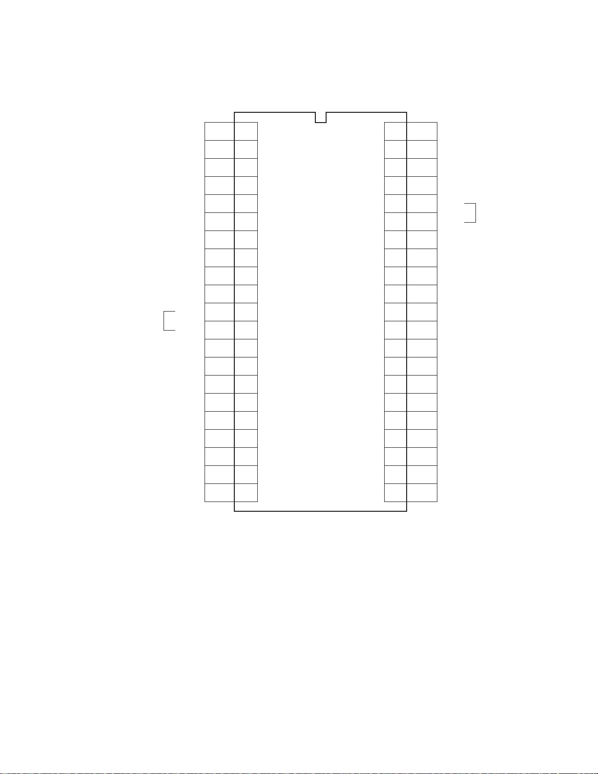
<< MICROCOMPUTER TERMINAL NAME AND OPERATION LOGIC >>
No. Terminal Name Function In/Out Logic Remarks
1 GND 0V
2 BAL INPUT BALANCE Out PWM out
3 REM OUT REMOTE CONTROL Out Remote control output
SIGNAL OUT
4 MUTE SOUND MUTE OUT Out Sound mute output
5 SP MUTE SPEAKER MUTE Out In muting = H
6 DEF POW Out
7 POWER POWER ON/OFF OUT Out Power control In ON=H
8 LED POWER LED OUTPUT Out Power LED on-control
LED lighting=L
9 POWER LNB Out 0V
10 LNB DET In 0V
11 SCL() IIC BUS CLOCK OUT Out IIC bus clock output 0
12 SDA() IIC BUS DATA IN/OUT In/Out IIC bus data input/output 0
13 SYNC VCD H SYNC INPUT In Main picture H. sync signal input
14
15 AFT2 IN In Sub tuner AFT S-curve input
16 AFT1 UV MAIN S-CURVE In Main tuner AFT S-curve
SIGNAL signal input
17 KEY A LOCAL KEY INPUT In Local key detection: 0 to 5V
18 KEY B LOCAL KEY INPUT In Local key detection: 0 to 5V
19 SGV TEST SIGNAL OUT Out Test signal output In normal=L 0V
20 SGA TEST AUDIO OUT Out Test audio output In normal=L 0V
21 VSS POWER GROUNDING — 0V: Gounding voltage 0V
22 R R Out At display on:Pulse
23 G G Out At dispaly on:Pulse
24 B B Out At dispaly on:Pulse
25 Y/BL BL Out At dispaly on:Pulse
26 HSYNC In HSYNC for OSD display Pulse
27 VSYNC In VSYNC for OSD display Pulse
28 OSC1 DISPLAY CLOCK Out 4.5MHz Pulse
29 OSC2 DISPLAY CLOCK In Pulse
30 TEST TEST MODE In GND fixed 0V
31 XIN SYSTEM CLOCK In System clock input 8MHz pulse
32 XOUT SYSTEM CLOCK Out System clock output 8MHz 8MHz pulse
33 RESET SYSTEM RESET In System reset input (In reset=L) 5V
34 SW IN
35 RMT IN REMOTE CONTROL IN In remote control pulse input=L In reception of
SIGNAL INPUT remote pulse
36 SYNC AV1 HSYNC INPUT In External H. sync signal input Pulse
37 SCL1 IIC BUS CLOCK OUT Out IIC bus clock output 1 Pulse
38 SDA1 IIC BUS DATA IN/OUT In/Out IIC bus data input/output 1 Pulse
39 GND 0V
40 NC
41 ACP NSYNC INPUT In AC pulse input
42 VDD POWER — 5V 5V
28
5. EEPROM (QA02)
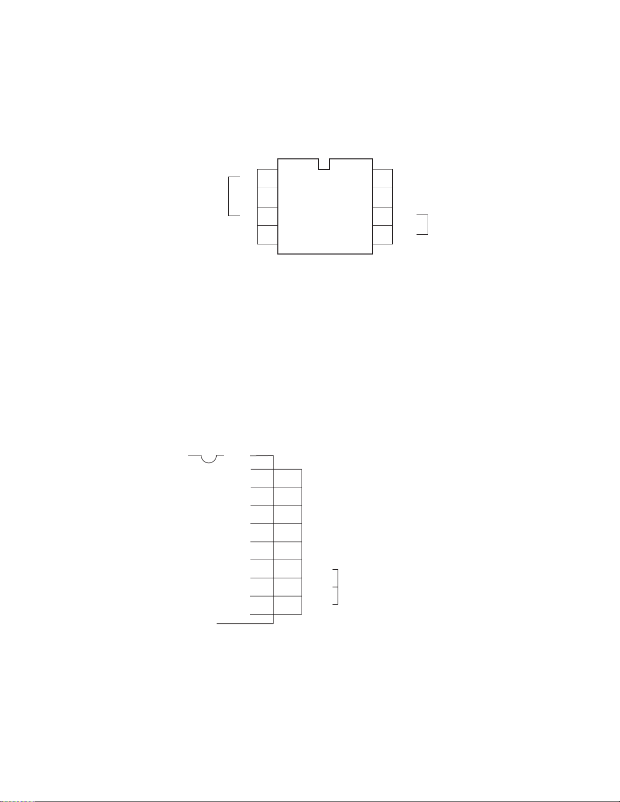
EEPROM (Non volatile memory) has function which, in spite of power-off, memorizes the such condition as channel selecting
data, last memory status, user control and digital processor data. The capacity of EEPROM is 8k bits. Type name is 24LC04BI/
P or ST24C04CB6, and those are the same in pin allocation and function, and are exchangeable each other. This IC controls
through I2C bus. The power supply of EEPROM and MICOM is common. Pin function of EEPROM is shown in Figure 3-3.
EEPROM(QA02)
1
Device adress
GND
A0
A1
A2
Vss
2
3
4
Fig. 3-3
8
7
6
5
Vcc + 5V
NC
SCL
SDA
2
C-BUS line
I
6. ON SCREEN FUNCTION
ON SCREEN FUNCTION indicates data like channel, volume. Formerly, exclusive use of OSD IC was used, but in N5SS,
OSD function is involved in microcomputer. Pin function concerning on-screen is shown in figure 3-4. Oscillation clock of OSD
is approx. 4.5MHz. 9MHz which becomes twice in microcomputer is dot clock. For oscillation coil, TRF1160D (LA02) is used.
QA01
OSC2
OSC1
Y/BL
VD
HD
O
29
OSC2 OSC OUT
I
28
OSC1 OSC IN
I
27
VSYNC H. SYNC SIGNAL
I
26
HSYNC V. SYNC SIGNAL
O
25
Ys/Ym HALF TONE SIGNAL
B
O
G
O
R
O
BOUT
24
23
GOUT COLOR SIGNAL
22
ROUT
G
V
Fig. 3-4
29
7. SYSTEM BLOCK DIAGRAM
TMP87CS38N-3152
QA01
QA02
MEMORY
24LC04B1/P
SDA SCL
5 6
H. SYNC PULSE
VSYNC PULSE
VIDEO SIGNAL
PROCESS
CIRCUIT
REMOTE CONTROL
OUTPUT
SOUND MUTE
SPEAKER MUTE
Q701
C/C, EDS
XC144144P
DATA CLK
11
12
26
27
22
23
24
25
3
4
5
SCL 0
SDA 0
HSYNC
VSYNC
R
G
B
YS/TM
RMT OUT
MUTE
SP MUTE
SDA 1
SCL 1
RMT
KEY-A
KEY-B
RST
VDD
GND
VSS
POWER
ACP
LED
XIN
XOUT
OSCI
OSCO
SGV
SGA
38
37
35
17
18
28
29
19
20
33
42
1
21
7
41
8
31
32
REMOTE
SENSOR
UNIT
KEY SWITCH
POWER
SUPPLY
CIRCUIT
8MHz
CLOCK
6.1MHz
CLOCK
SIGNAL
OUTPUT
H001
MAIN U/V TUNER
EL446L
SDA SCL
HY01
SUB U/V TUNER
EL922L
SDA SCL
Q501
VCD
TA1222
SDA SCL
27 28
H002
IF/MPX
MVUS345
SDA SCL
21 20
DPC UNIT
DATA CLK
QY04
PIP CONTROL
DATA CLK
6 5
SYNC-AV1
AFT1 IN
SYCN-AV2
AFT2 IN
36
16
13
Fig. 3-5
30
MAIN SCREEN
SUB SCREEN
2
SYNC DET.
AFT DET.
SYNC DET.
AFT DET.
QV01
AV SW
TA1219N
SDA SCL
26 27
QM01
DSP
SDA SCL
 Loading...