

Page 1
NTDPJTV04
SERVICETRAINING
"CustomerSatisfactionThroughKnowledge"
SERVICINGTHEN5SS
COLORTELEVISION
CHASSIS/DIGITAL
CONVERGENCE
TOSHIBAAMERICACONSUMERPRODUCTS,INC.
NATIONALSERVICEDIVISION
TRAININGDEPARTMENT
1420-BTOSHIBADRIVE
LEBANON,TENNESSEE37087
PHONE:(615)449-2360
FAX:(615)444-7520
Page 2

FOREWORD
The material presented in this manual is provided for the technical training of T ACP employees and
qualified service personnel only .
The specific circuit reference designations, pin numbers, etc., are taken from the TP48E50/60 Service
Manual, File Number 020-9508. The diagrams in this manual are simplified for training and should be used
as a reference guide only when servicing the N5SS CTV Chassis. Refer to the applicable service data for
detailed adjustment and servicing procedures.
NTDPJTV04
SERVICING T OSHIBA'S N5SS TELEVISION CHASSIS
©1996
TOSHIBA AMERICA CONSUMER PRODUCTS, INC.
National Service Division
National Training Department
1420 T oshiba Drive
Lebanon, TN 37087
(615) 449-2360
No part of this manual may be reproduced in whole or in part without prior written consent from
Toshiba America Consumer Products, Inc., Service Division.
Page 3

CONTENTS
SECTION I
OVERALL UNIT CHARACTERISTICS,
BLOCK DIAGRAMS, LABS 1 & 2
1.MAIN FEATURES..................................1-2
2.MERITS OF BUS SYSTEM....................1-2
2-1.Improved Servciceability.................1-2
2-2.Reduction of Parts Count................1-2
2-3.Quality Control.................................1-2
3. COMPARISON/DIFFERENCES TG-1...1-2
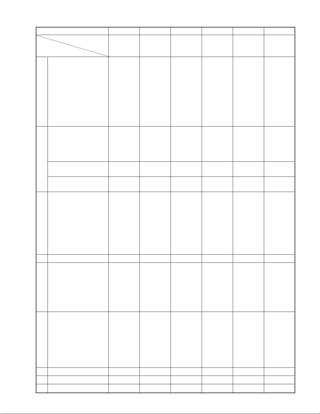
4.SPECIFICATIONS..................................1-3
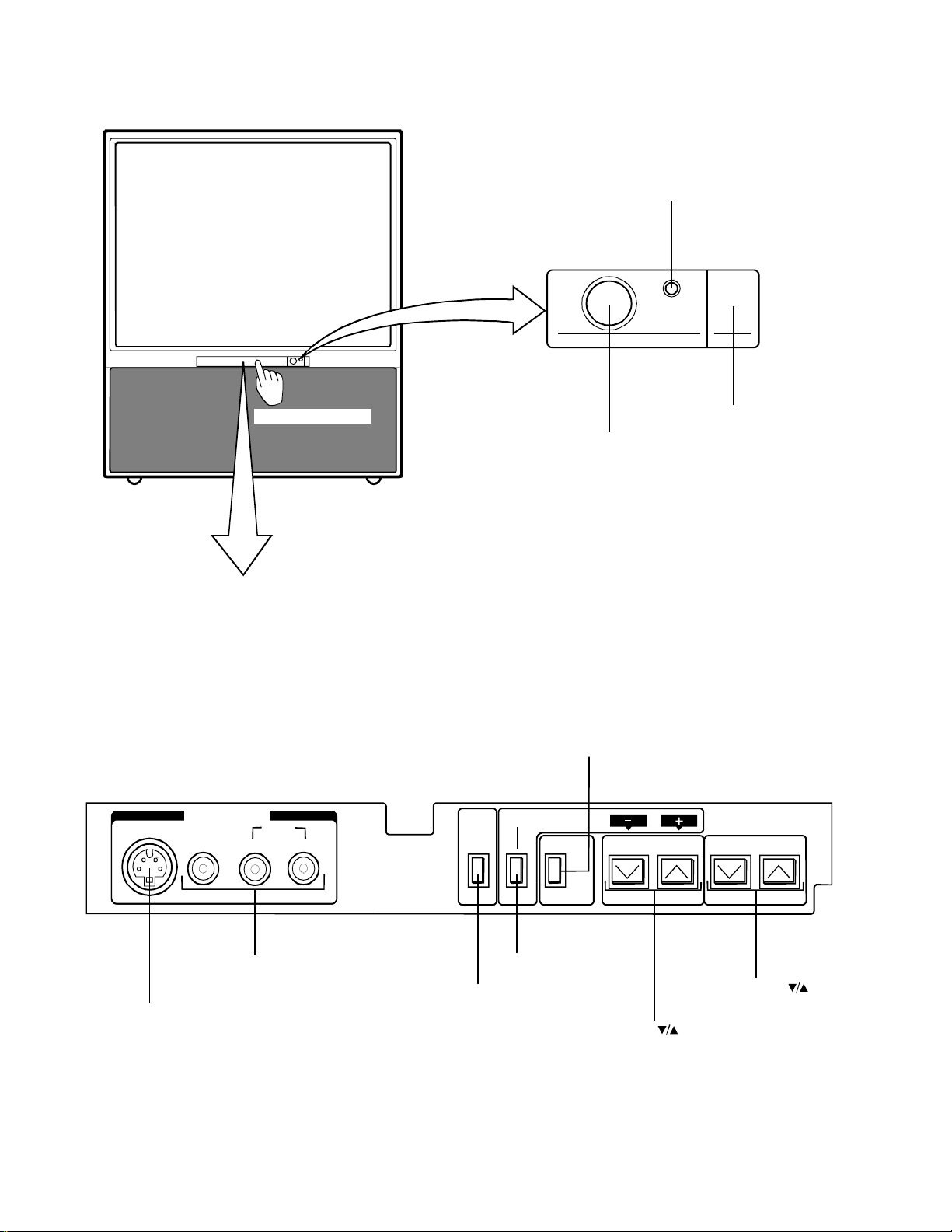
5.FRONT AND REAR CONTROL
VIEWS.....................................................1-4
5-1.Front View........................................1-4
5-2.Rear View.........................................1-5
5-3.Remote Control View.......................1-6
6.'95 PJ-TV CHASSIS LAYOUT...............1-7
7.CONSTRUCTION OF CHASSIS............1-8
8. VIDEO SIGNAL FLOW........................1-9
9.AUDIO SIGNAL FLOW.......................1-11
10.POWER SUPPLY..................................1-12
11.H and V DEFLECTION.........................1-13
12.I2C COMMUNICATIONS.....................1-14
13.DIGITAL CONVERGENCE.................1-15
14.LAB 1.....................................................1-16
15.LAB 2.....................................................1-20
SECTION II
TUNER, IF/MTS/S.PRO MODULE
1.CIRCUIT BLOCK....................................2-2
1-1.Outline..............................................2-2
1-2.Major Features..................................2-2
1-3.Audio Multiplex Demodulation
Circuit...............................................2-3
1-4.A.PRO Section (Audio Processor)...2-4
2.PIP TUNER..............................................2-6
2-1. Outline...............................................2-6
SECTION III
CHANNEL SELECTION CIRCUIT
1.OUTLINE OF CHANNEL
SELECTION CIRCUIT SYSTEM..........3-2
2.OPERATION OF CHANNEL
SELECTION CIRCUIT...........................3-2
3.MICROCOMPUTER...............................3-3
4.MICROCOMPUTER TERMINAL
FUNCTION..............................................3-4
5.EEPROM (QA02)....................................3-6
6.ON SCREEN FUNCTION.......................3-6
7.SYSTEM BLOCK DIAGRAM................3-7
8.LOCAL KEY DETECTION METHOD..3-8
9. ENTERING THE SERVICE MODE.......3-9
10.TEST SIGNAL SELECTION..................3-9
11.SERVICE ADJUSTMENT......................3-9
12.FAILURE DIAGNOSIS PROCEDURE3-10
13.TROUBLE SHOOTING CHARTS.......3-13
SECTION IV
AUDIO OUTPUT CIRCUIT
1.OUTLINE.................................................4-2
2.THEORY OF OPERATION....................4-2
2-1.Operation of TA8256H....................4-2
SECTION V
DSP CIRCUIT
1.ORIGINS OF DOLBY SURROUND......5-2
2.THE DOLBY MP MATRIX....................5-2
3.THE DOLBY SURROUND
DECODER...............................................5-3
4.DSP CIRCUIT..........................................5-3
5.DSP (Digital Surround Processor) IC......5-6
SECTION VI
A/V SWITCHING CIRCUIT
1.OUTLINE.................................................6-2
2.IN/OUT TERMINALS............................6-2
3.CIRCUIT OPERATION..........................6-2
3-1.Composite Video Signal...................6-2
3-2.S-Video Signal.................................6-2
SECTION VII
VIDEO PROCESSING CIRCUIT
1.OUTLINE.................................................7-2
2.SIGNAL FLOW.......................................7-2
3.CIRCUIT OPERATION..........................7-2
SECTION VIII
V/C/D/IC
1.OUTLINE.................................................8-2
2.LARGE SCALE EMPLOYMENT OF
BUS CONTROL OF PARAMETER FOR
PICTURE CONTROLS...........................8-2
3.EMPLOYMENT OF CONTAINING
EACH VIDEO BAND FILTER
INSIDE.....................................................8-2
Page 4

4. EMPLOYMENT OF CONTAINING
EACH FILTER (FOR S/H) INSIDE ....... 8-2
5. LOW COST OF IC ..................................8-3
SECTION IX
PIP MODULE
1. BOARD LAYOUT...................................9-2
2. SIGNALS .................................................9-2
3. BLOCK DIAGRAM ................................9-3
SECTION X
SYNC SEPARATION, H-AFC,
H-OSCILLATOR CIRCUITS
1. SYNC SEPARATION CIRCUIT .......... 10-2
1-1. Theory of Operation .......................10-2
2. H AFC (Automatic Frequency Control)
CIRCUIT ................................................10-3
3. H OSCILLATOR CIRCUIT ..................10-4
3-1. Outline ............................................10-4
3-2. Theory of Operation .......................10-4
SECTION XI
VERTICAL OUTPUT CIRCUIT
1. OUTLINE...............................................11-2
1-1. Theory of Operation .......................11-2
2. V OUTPUT CIRCUIT ...........................11-3
2-1. Actual Circuit .................................11-3
2-2. Sawtooth Waveform Generation ....11-3
2-3. V Output .........................................11-4
2-4. V Linearity Characteristic
Correction .......................................11-6
3. PROTECTION CIRCUIT FOR
V DEFLECTION STOP ........................ 11-7
3-1. +35V Over Current
Protection Circuit ...........................11-8
SECTION XII
HORIZONTAL DEFLECTION CIRCUIT
1. OUTLINE...............................................12-2
2. HORIZONTAL DRIVE CIRCUIT........12-2
2-1. Theory of Operation .......................12-2
3. BASIC OPERATION OF HORIZONTAL
DRIVE....................................................12-3
3-1. Theory of Operation .......................12-3
3-2. Drive System ..................................12-4
3-3. Circuit Description .........................12-5
4. HORIZONTAL OUTPUT CIRCUIT ....12-6
4-1. Theory of Operation .......................12-7
4-2. White Peak Bending
Correction Circuit.........................12-11
4-3. H Blanking ...................................12-12
4-4. 200V Low Voltage Protection......12-13
5. HIGH VOLTAGE GENERATION
CIRCUIT ..............................................12-14
5-1. Theory of Operation .....................12-14
5-2. Operation Theory of the Harmonic
Non-Resonant System and Tuned
Waveforms ...................................12-16
6. HIGH VOLTAGE CIRCUIT ...............12-17
6-1. High Voltage Regulator................12-17
7. X-RAY PROTECTION CIRCUIT ...... 12-20
7-1. Outline ..........................................12-20
7-2. Operation ......................................12-20
8. OVER CURRENT PROTECTION
CIRCUIT ..............................................12-21
8-1. Outline ..........................................12-21
8-2. Operation ......................................12-21
SECTION XIII
DEFLECTION DISTORTION
CORRECTION CIRCUIT (DPC Circuit)
1. DEFLECTION DISTORTION
CORRECTION IC (TA8859P) ..............13-2
1-1. Outline ............................................13-2
1-2. Functions and Features ...................13-2
1-3. Block Diagram ...............................13-2
2. DIODE MODULATOR CIRCUIT ........13-3
3. ACTUAL CIRCUIT...............................13-4
3-1. Basic Operation and Current Path ..13-5
SECTION XIV
CLOSED CAPTION/EDS CIRCUIT
1. OUTLINE...............................................14-2
2. DATA TRANSMISSION FORMAT.....14-2
3. DISPLAY FORMAT ............................. 14-3
4. CIRCUIT OPERATION ........................14-4
SECTION XV
DIGITAL CONVERGENCE CIRCUIT
1. OUTLINE...............................................15-2
2. CIRCUIT DESCRIPTION .....................15-2
2-1. Configuration..................................15-2
2-2. Circuit Operation ............................15-2
3. PICTURE ADJUSTMENT ....................15-4
3-1. Change of Memory (E2PROM) ......15-4
3-2. Service Mode ..................................15-4
4. ADJUSTING PICTURE
DIMENSION (Green picture)................15-6
5. KEY FUNCTION OF REMOTE CONTROL
UNIT ......................................................15-7
6. CONVERGENCE OUTPUT
CIRCUIT ................................................15-8
6-1. Outline ............................................15-8
Page 5

6-2. Circuit Description .........................15-8
7. CONVERGENCE TROUBLESHOOTING
CHART.................................................15-10
8. LAB 3 ...................................................15-11
SECTION XVI
OPTICAL SECTION
1. NECK COMPONENTS .........................16-2
1-1. Outline of Components Around
Neck of The Projection Tube .........16-2
1-2. Theory of Operation........................16-2
1-3. Projection Tube ..............................16-3
2. FUNCTION OF KEY
COMPONENTS .....................................16-4
2-1. Outline ............................................16-4
2-2. Theory of Operation .......................16-4
2-4. Optical Coupling Effect .................16-8
2-5. Lens ................................................16-9
2-6. Focus Adjustment .........................16-10
SECTION XVII
POWER CIRCUIT
1. OVERVIEW...........................................17-3
2. RECTIFYING CIRCUIT AND
STANDBY POWER SUPPLY ..............17-4
3. MAIN SUPPLY CIRCUIT .................... 17-4
4. OUTLINE OF CURRENT RESONANT
TYPE SUPPLY ......................................17-4
5. FUNDAMENTAL THEORY ................17-5
6. ACTUAL CIRCUIT...............................17-6
7. SCAN DERIVED VOLTAGES.............17-8
8. PROTECTOR MODULE (Z801) ..........17-9
9. SUB POWER SUPPLY .......................17-10
10. PROTECT CIRCUITS .........................17-11
11. LAB 4 ...................................................17-15
SECTION XVIII
DYNAMIC FOCUS CIRCUIT
1. OUTLINE...............................................18-2
2. H DYNAMIC FOCUS CIRCUIT ..........18-2
2-1. Theory of Operation .......................18-2
2-2. Circuit Operation ............................18-3
3. V DYNAMIC FOCUS CIRCUIT ..........18-4
3-1. Theory of Operation .......................18-4
3-2. Circuit Operation ............................18-5
Page 6

SECTION I
OVERALL UNIT
CHARACTERISTICS
BLOCK DIAGRAMS
LABS 1 & 2
1-1
Page 7
SECTION I
OVERALL UNIT
CHARACTERISTICS
1. MAIN FEATURES
The main feature of Toshiba's projection television model
TP48E60, is the use of the N5SS (TG-1C) chassis. This
chassis utilizes a bus control system, developed by PHILIPS
Corporation, called the I2C (or IIC) bus. IIC stands for InterIntegrated Circuit control. This bus co-ordinates the transfer
of data and control between ICs inside the Television. It is a
bi-directional serial bus consisting of two lines, namely SDA
(Serial DATA), and SCL (Serial CLOCK).
Digital data which is passed along the bus is received by
individual devices and can be either command or data.
Digital-to analog converters are also found within some of
the ICs, allowing them to be addressed and controlled by
strings of digital instructions, replacing those functions
which were previously implemented by external
potentiometers.
2. MERITS OF THE BUS SYSTEM
2-1. Improved Serviceability
Most of the adjustments previously made by resetting variable
resistors and/or capacitors can be made on the new chassis
by operating the remote control and seeing the results on the
television screen. This allows adjustments to be made without
removing covers on the unit thus increasing servicing speed
and efficiency.
2-2. Reduction of Parts Count
The use of digital-to-analog converters built into the ICs,
allowing them to be controlled by software, has eliminated
or reduced the requirement for many discrete parts such as
potentiometers and trimmers, etc.
2-3. Quality Control
The central control of adjustment data makes it easier to
understand, analyze, and review the data, thus improving
the quality of the product.
3. COMPARISON/DIFFERENCES OF TG-1 CHASSIS
Toshiba's concept for the TG-1 chassis was to create a sort
of universal chassis which, with minimal changes, could be
used as a standard throughout the entire Toshiba color
television lineup starting in 1995. TG-1 stands for "Toshiba
Global 1". The TG-1 chassis can be found in several
different models and varies in both complexity and features.
Ro ot TG-1 Typical Pic ture and
Chassis Chassis Sizes Features
N5E A1 13, 19 Less
N5ES A2 20, 32
N5S A2 - LEM 20, 32
N5S B 27, 32
N5SS C 27 thru 35 More
Typical Chassis Ex am ples
Model TG-1
CF13E22,23 A1
CF19E22 A1
CF20E30 A1
CF20E40 A1
CN27E55 A 2
CF30E50 A2
CF32E50 A2
CF32E55 A2
CX32E60 B
CX32E60 B
CN27E90 C
CX32E70 C
CN32E90 C
CN35E15 C
TP48E50,51 C
TP48E60,61 C
TP55E50,51 C
TP55E80.81 C
TP61E80 C
TP48E90 C
1-2
Page 8
4. SPECIFICATIONS
CHASSIS CCCCCC
MODEL Nbr TP48E50 TP48E60 TP48E90 TP55E50 TP55E80 TP61E80
TP48E51 TP48E61 TP55E51 TP55E81 STEP-UP
SPECIFICATION
1 Picture Size# 48"-D/S 48"-D/S 48"-D/S 55"-D/S 55"-D/S 61"-D/S
2 Channel Capacity 181ch 181ch 181ch 181ch 181ch 181ch
*
3 C. Caption ●●●●●●
G
4 MTS with dbx ●●●●●●
E
N
5 Bass, Tre/Balance ●●●●●●
E
6 Sub-Audio-Program ●●●●●●
R
7 Remote Control *A-Uni (42k A-Uni (42k *Intelig+EZ A-Univ (42k A-Univ (43k A-Univ (43k
A
8 Picture-in-Picture * ●
L
9 LED Indicator (RED) ● (P) ● (P) ● (P) ● (P) ● (P) ● (P)
10 Local Key 8key 8key 8key 8key 8key 8key
11 Dolby Surround — — ●(Prolo) — ●●
12 Dig-Sound Processor — — ● (DSP4ch) — ● (DSP4ch) ● (DSP4ch)
*
13 Front Surround ●●—●——
S
14 Cyclone ABX ——————
O
15 Sub-Bass-System ●●●●●●
U
16 Audio Output 14Wx2 14Wx2
N
D
17 Speaker Size & Nbr 160Rx2 160Rx2 160Rx2 160Rx2 160Rx2 160Rx2
18 Comb Filter ●
*
19 Dynamic Focus # ●●●●●●
P
20 Scan Velocity Modu ●
I
21 Vert Contour Corre ——————
C
22 Black Level Expand ●●●●●●
T
23 Flesh Tone Correct ●●●●●●
U
R
24 Dynamic Noise Reduc ●●●●●●
E
25 Picture Preference ●●●●●●
26 Digital-Convergence ●●●●●●
27 Horiz Resolution 800 800 800 800 800 800
28 Parental-Ch Lock ●●●●●●
*
29 Channel Label (32ch) ●●●●●●
O
30 3-Language Display ●●●●●●
T
31 Clock/Off-Timer ● / ●●/●●/●●/●●/●●/●
H
32 Favorite Channel ●●●●●●
E
R
33 Extended-Data-Servi ●●●●●●
34 Star-Sight-Decoder ——————
35 S-Video In-Term ●
36 Audio, Video-In/Out 1+2/1 1+2/1 1+2/1 1+2/1 1+2/1 1+2/1
*
37 Front AV Jack ●●●●●●
T
E
38 Variable Audio Out ●●●●●●
R
39 2-RF Input *— ●●—●●
M
40 Ext Speaker Term ●●●●●
S
41 PIP Audio Out Jack — — ● ———
42 Center-Ch-Aud-Input ————●●
43 Speaker-Box — — ● (SS-SR94 — ● (SS-SR94 ● (SS-SR94
AC
*Cabinet NEW NEW NEW NEW NEW NEW
PARTS SUPPLY (ISO) ——————
(1TN)
(DIG)
(RGB)
(1+1)
●
●
●
●
(2TN)
(DIG)
(RGB)
(1+1)
●
(2TN)
14Wx2, 10Wx2
& 10Wx2
& REAR SPK & REAR SPK & REAR SPK
●
(DIG)
●
(RGB)
●
(1+1)
●
(1TN)
14Wx2 14Wx2 14Wx2
●
(DIG)
●
(RGB)
●
(1+1)
●
(2TN)
& 10Wx2 & 10Wx2
●
(DIG)● (3D-Y/C)
●
(RGB)
●
(1+1)
●
●
●
(2TN)
(RGB)
(1+1)
1-3
Page 9
5. FRONT AND REAR CONTROL VIEWS
5-1. Front View
POWER indicator
POWER
S-VIDEO
Press to open the door.
Behind the door
IN-VIDEO 3
VIDEO
L/MONO R
AUDIO
Fig. 1-1
DEMO
POWER button
ANT/VIDEO button*
ADV butto n
MENU-ADV
ANT/VIDEO
VOLUME
Remote se ns or loca tio n
CHANNEL
VIDEO/AUDIO INPUT
jacks
S-VIDEO INPUT jack
* These buttons have dual functions.
MENU buttom
DEMO button
Fig. 1-2
1-4
VOLUME buttons*
butto ns
−/+
CHANNEL
butttons
Page 10
1-5
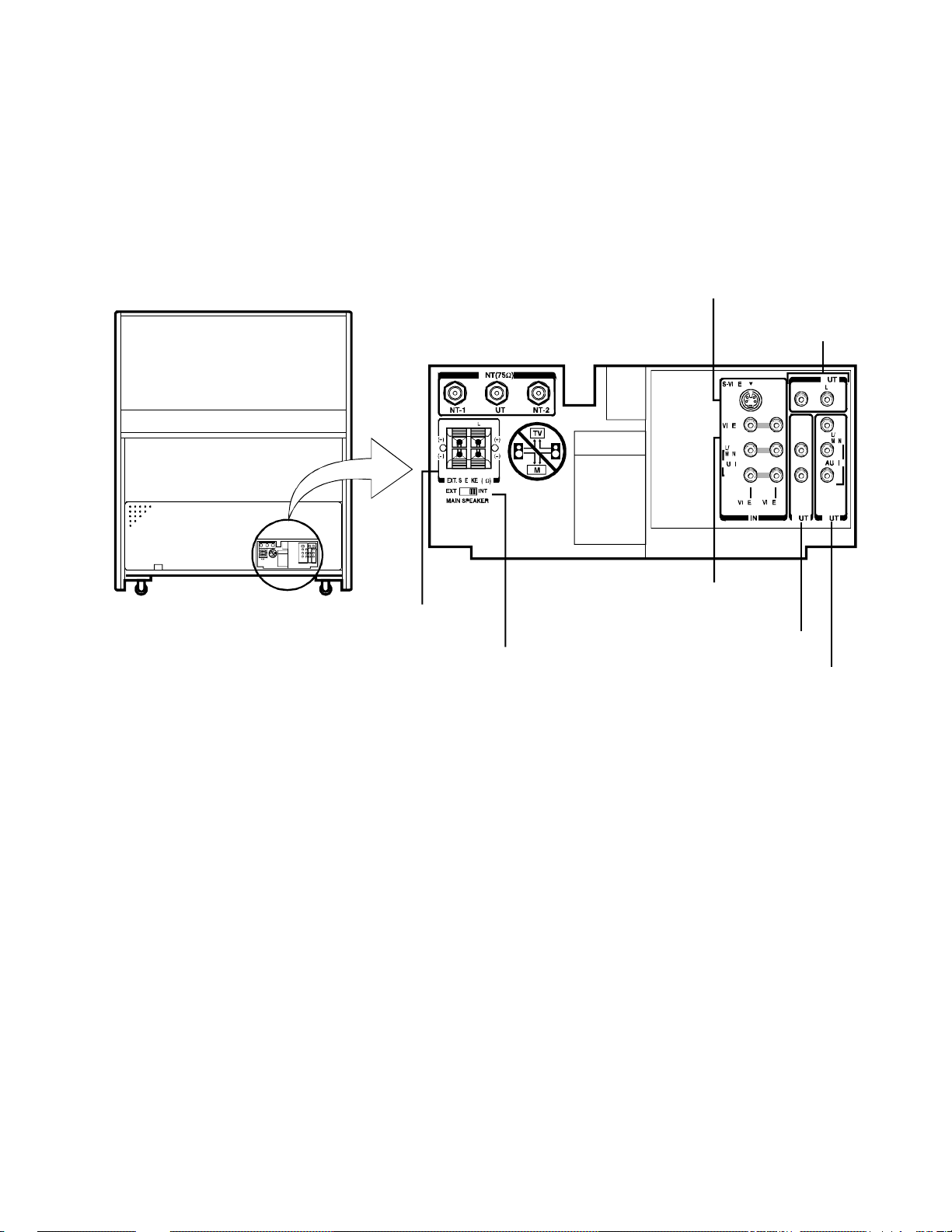
5-2. Rear View
OUTPUT jacks
TV rear
EXTERNAL
SPEAKER
terminals
A
A AO
R
A RP 8
MAIN
SPEAKER
switch
A P
S-VIDEO INPUT jack
D
O
D O
O O
D OA
R
O1 D O2
D
VIDEO 1 INPUT
jacks
VIDEO 2 INPUT
jacks
VARIABLE AUDIO
OUTPUT jacks
O
VAR
R
AUDIO
VIDEO
O O
L/MONO
AUDIO
O
D
R
R
PIP
OO
VIDEO/AUDIO
Fig. 1-3
Page 11
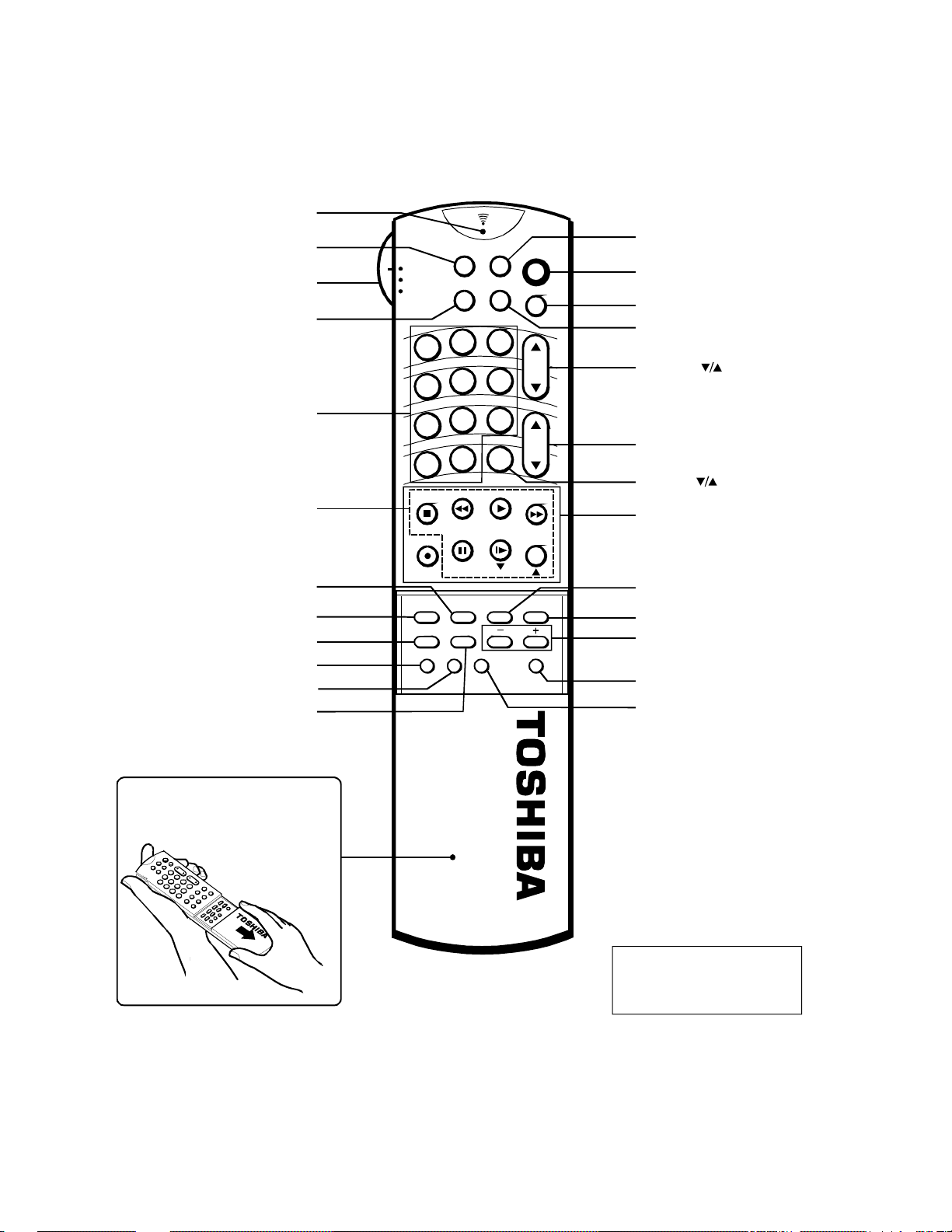
5-3. Remote Control View
y
y
y
Transmit indicator
TV/CABLE/VCR switch
Channel Number*
EDS*
TV/VIDEO*
PIP function*
AUDio*
PICture*
RESET*
C. CAPT*
ANT1/2*
EXIT*
S
D
E
V
T
E
L
B
A
C
R
C
V
1
4
7
100
STOP
LOCATE
REC
PIC.
RESETEXIT
C.CAPTANT1/ 2CYC/ SBS DSP/SUR
O
E
D
I
V
/
V
T
2
5
8
0
REW
SW APSOURCE
PAUSE/ STI LL
SLOW
STILL
AUD.SET UP
R
R
E
C
A
3
6
9
ENT
RTN
PLAY
FAV
O
W
L
L
M
U
T
E
CH
VOL
FF
PIP
TV/VC R
PIP
CH
OPTION
E
P
M
I
T
E
TIMER/Clock*
R
POWER
RECALL*
MUTE*
CHANNEL
RTN*
VOLUME
VCR function*
SET UP*
OPTION*
−/+
FAV −/+*
DSP/SUR*
SYC/SBS*
To operate buttons inside the cover,
slide the cover down and toward
ou.
*
These functions do not have
duplicate locations on the TV.
can be controlled only b
The
the Remote Control.
Fig. 1-4
1-6
Page 12
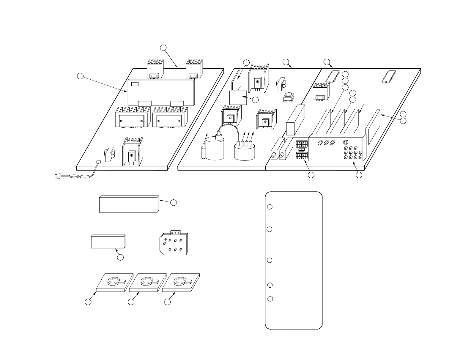
6. PJTV CHASSIS LAYOUT
3
1-7
Fig. 1-5
:DIGITAL CONVER
8
-1:CRT-D(R)
5
5
REAR
AMP 2CH
-5:SVH
-4:CRT-D(G)
5
-4:FRONT
5
FOCUS PACK
-4:CRT-D(B)
5
:CONV/POW2
CENTER
AMP 2CH
to FOCUS
PACK
F.B.T
-4:DYNAMIC FOCUS
4
to CRT
J-BOX
3:DPC
−
3
1. AUDIO
7A
7B
2. COMB FILTER
:DEF/POWER
1
FEATURE
FRONT SURROUND
TP48E50/51/60/61
TP55E50/51
* SPK. TREM. 1pcs
* REAR.CENTER AMP W/O
:DSP4CH
TP55E80/81
TP61E80
* SPK TERM. 2pcs
* REAR. AMP W/
* CENTER. AMP W/O
* CENTER INPUT W/
:DOLBY PRO
9
TP48E90
* SPK. TERM. 2pcs
* REAR. CENTER AMP W/
:DIGITAL COMB
6A
TP48E50/51/60/61/90
TP55E50/51
:3D Y/C TP61E80
6B
3. TUNER
* TP48E50/51
* TP55E50/51ONLY
1 TUNER
OTHER 2 TUNER
FRONT
AMP 2CH
-2:SPEAKER
4
2
:MAIN
-1:FRONT SURRO UND
7A
-1:DSP 4CH
7B
:DOLBY PRO
9
:DIGITAL COMB
6A
:3D Y/C
6B
PIP(HOKURIKU)
-1:A/V
4
-2:EDS.CC
7A
-2:EDS.CC
7B
Page 13
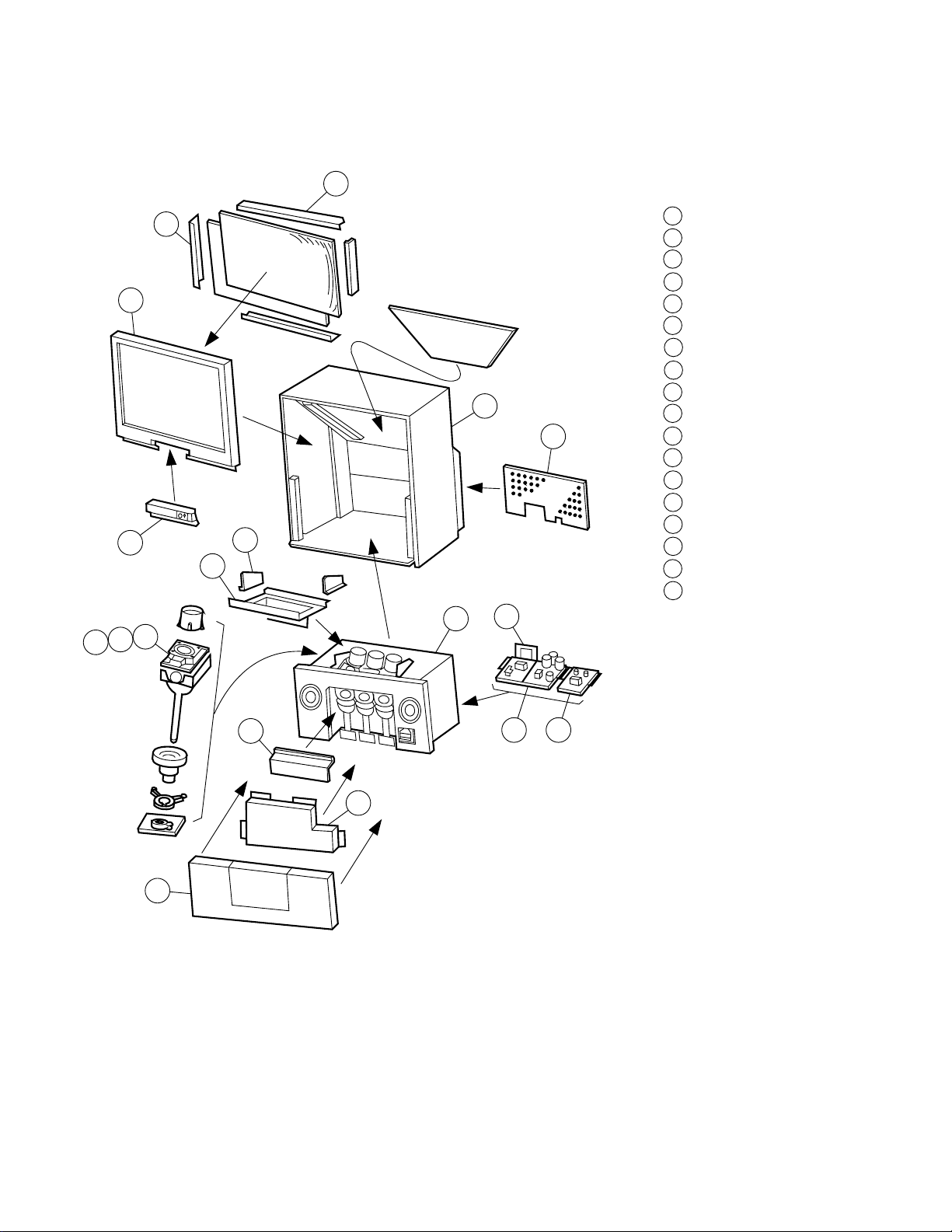
7. CONSTRUCTION OF CHASSIS
9
10
8
7
5
13
14
11
15
WOOD CABINET
1
LIGHT BOX
2
SPEAKER GRILLE
3
FRONT COVER
4
CRT MOUNTING
5
SHIELD FRONT
6
SHIELD SIDE
7
SCREEN BEZEL
8
SCREEN BRACKET L
1
12
2
18
9
SCREEN BRACKET S
10
CONTROL PANEL
11
BACK BOARD
12
COUPLING R
13
COUPLING G
14
COUPLING B
15
CHASSIS FRAME MAIN
16
CHASSIS FRAME POWER
17
AV TERMINAL BOARD
18
6
4
3
16 17
Fig. 1-6
1-8
Page 14

8. VIDEO SIGNAL FLOW BLOCK DIAGRAM
Basic Circuit Operation
The basic operation of the TG-1 chassis is illustrated in the
block diagrams, figures 1-7 through 1-12. Although these
diagrams focus on the TP48E60, the video and audio signal
flow diagrams can be applied to any TG-1 chassis with
minor modifications.
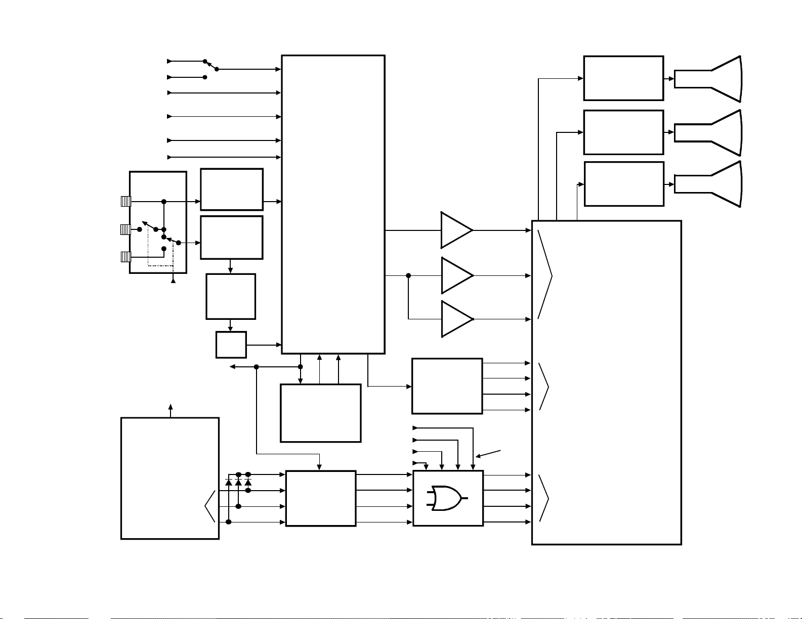
Video Signal Flow
Figure 1-7 illustrates the video signal flow through the TG1 chassis. The Antenna 1 (ANT 1) and Antenna 2 (ANT
2) inputs allow two separate RF signals to be connected to
the RF switcher. When the switch, which is controlled by
the microcomputer, QA01, is in the up position the ANT 1
signal is connected to the HY01 PIP Tuner/IF and the H001
Main Tuner. Moving the switch down connects the ANT
2 signal to the H001 Tuner. Due to the RF Switch the ANT
2 signal can’t be used as the PIP source, but when ANT 2
is selected the ANT 1 signal is available at RF OUT. The
PIP Tuner/IF produces a composite video (CV) signal and
sends it to the AV Switcher, QV01. An IF signal produced
by the Main Tuner is sent to H002, which produces a
composite video signal and sends it to the AV Switcher.
Three video inputs, video 1 through 3, are applied to the AV
Switcher. The video 1 input can be composite video, Y/C
video, or the test signal from QA01. Video 2 is composite
video only, and video 3 is either composite video or Y/C
video. A mechanical switch on the video 1 input defaults
to the test signal, so a video connector must not be plugged
into the video 1 input jack when the internal test signals are
used.
The selected video signal is output as composite video and
applied to the video output jack, the EDS/CC/RGB SW.,
and the Digital Comb Filter or the 3D - Y/C circuit. After
processing the video signal is sent back to the AV Switcher
as separate luminance (Y) and chrominance (C) signals.
The Y and C signals are then sent to Q501 the Video
Chroma Deflection Processing IC. A sync signal is tapped
off the Y signal and applied to Q501. Q501 processes the
video signal and sends separate R, G, and B signals to the
CRT drives and the CRTs.
If the PIP feature is selected, composite video from AV
Switcher is sent to the PIP circuit, ZY01. After processing,
the PIP signal is sent to Q501 as R, G, B, and YS where it
is mixed with the main video.
On screen display (OSD) R, G, and B signals produced by
the Microcomputer, QA01, are mixed with the Extended
Data Service (EDS) and Closed Caption (CC) data in
UM01. These new signals are applied to an OR gate,
QB91, and combined with the convergence signals from
the digital convergence circuit. The convergence signals
can be either the customer convergence cross hairs, or the
service cross hatch pattern. All of these signals are sent to
Q501 where they are mixed with the main video signal.
1-9
Page 15
1-10
TEST
VIDEO 1
VIDEO 2
VIDEO 3
Figure 1-7 Video Signal Flow Block Diagram
ANT 1
RF
OUT
ANT 2
CV/Y
C
CV
CV/Y
C
RF
SWITC H
CONTROL
FROM
QA01
HY01 PIP
TUNER/IF
H001
MAIN
TUNER
IF
2
H002
IF/MTS
A. PRO
7
EQ
CV TO VIDEO
OUT JAC K
TEST SIGNAL
TO VIDEO 1
QA01
MICRO
COMPUTER
OSD
DATA
22
23
24
12
14
QV01
16
SWITCHING
18
15
CV
28
7
CV
38 30 32
CV
6
DIGITAL
COMB
FILTER
OR, 3D - Y/C
YS
R
G
B
18
19
20
21
9
UM01
EDS/CC
RGB SW.
AV
Y
2
CV
E031Z
9
RED CRT
RED CRT
DRIVE
E032Z
3
GREEN CRT
GRN CRT
DRIVE
E033Z
9
BLUE CRT
B
G
R
42 41
C
34
YY
36
Q503
Q202
SYNC
Q204
43
C
13
MAIN VIDEO
15
17
INPUT
VIDE O CHROMA
DRIVE
Q501
BLUE CRT
DEFLECTION
42
C
4
CV
ZY01
8
PIP
YS
R
G
B
10 13
YS
6
1
5
2
2
R
12
G
5
B
9
4
OR
QB91
1
4
R
5
G
B
6
FROM
DIGITAL
CONV.
1
3
11
6
8
YS
G
B
35
34
33
36
R
39
38
37
32
YS
PROCESSING
PIP VIDEO
INPUT
OSD, EDS, CC, &
CONVERGENCE
VIDEO INPUT
Page 16
9. AUDIO SIGNAL FLOW BLOCK DIAGRAM
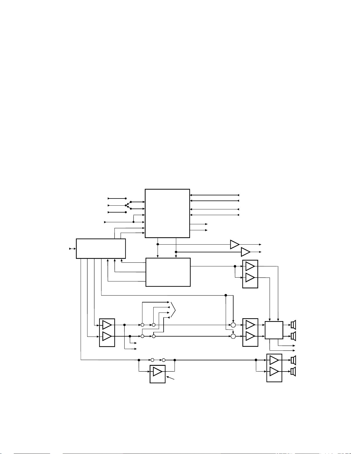
Audio Signal Flow
Audio signals are applied to the AV Switcher from the
three video jacks, H002, and the PIP Tuner, as shown in
Figure 1-8. Like the video signal, there must not be a
connector in the video 1 jack for the audio test signal to be
applied to the AV Switcher. In the TP48E90, PIP audio is
applied to the PIP output jack. The main audio signals are
applied to the audio output jacks and to the Front Surround
circuit, the DSP/Dolby circuit, or the Dolby Pro Logic
circuit. Afterprocessing, the left and right audio signals
are applied to the audio processor in H002 where the
volume, balance, treble, and bass are controlled. Next, the
audio signals are amplified by QS101 and applied to the
variable output jacks, and Q601. If the sub bass system
(SBS) is selected, a signal is mixed with the left and right
signals just before Q601 to increase the signals bass
response. In TP55E80/81 and TP61E80 models, the
jumper is removed so a center signal can be switched in to
replace the main left and right signals. The amplified left
and right audio signals are applied to the internal/external
speaker switch and routed to the desired speakers.
Sets equipped with Dolby or Dolby Pro Logic have a
surround audio signal that is sent to the audio processor in
H002 from the Dolby circuit. The surround signal is then
sent to the rear amplifier, Q641, amplified, and applied to
the rear speakers. In the TP48E90 the surround signal is
routed through an amplifier in Q690 before it is applied to
Q641. Also, the TP48E90 is equipped with Dolby Pro
Logic, and has a center channel. The center channel is
amplified by the Center Amplifier, Q621, and applied to
the front speakers through the internal/external speaker
switch.
VIDEO 1
IF
FROM H001
MAIN TUNE R
SURROUND
TP48E90
TP55E80/81
TP61E80
TEST SIGNAL
FROM QA01
MONO AUDIO
FROM HY01
PIP TUNER
L
R
H002
IF/MTS/A. PRO
2326242217 16 18
L
R
5
L
3
R
QS101
11
13
29
31
L
5
6
R
L
6
R
SURROUND OUT
SBS (SUB BASS SYSTEM)
7
1
5
10
R
TO VARIABLE AUDIO
L
QV01
AV
SWITCHING
37 35
3
DSP/DOLBY,
OR
1
Q690
R
2
TO &FROM CEN TER
INPUT SWITCH & JACK
TP55E80/81 & TP61E80
TP48E90
ONLY
L
FRONT SURROUND,
DOLBY PRO LOGIC
OUT JACK
3
8
9
15
17
1
2
11
CENTER OUT
ONLY
L
TO PIP OUT JACK
(TP48E90 ONLY)
R
QS04
L
R
L
R
QV14
2
4
Q621
CENTER AMP
TP48E90 ONLY
5
+
2
+
Q601
VIDEO 2
VIDEO 3
L
R
12
7
7
INT/EXT
L
SWITCH
11
R
2
4
REAR AMP
TO AUDIO
OUT JACK
RL
Q641
12
7
FRONT OR
CENTER
SPEAKERS
EXTERNAL
REAR
SPEAKERS
Figure 1-8 Audio Signal Flow Block Diagram
1-11
Page 17
10. POWER SUPPLY AND PROTECTION BLOCK DIAGRAM
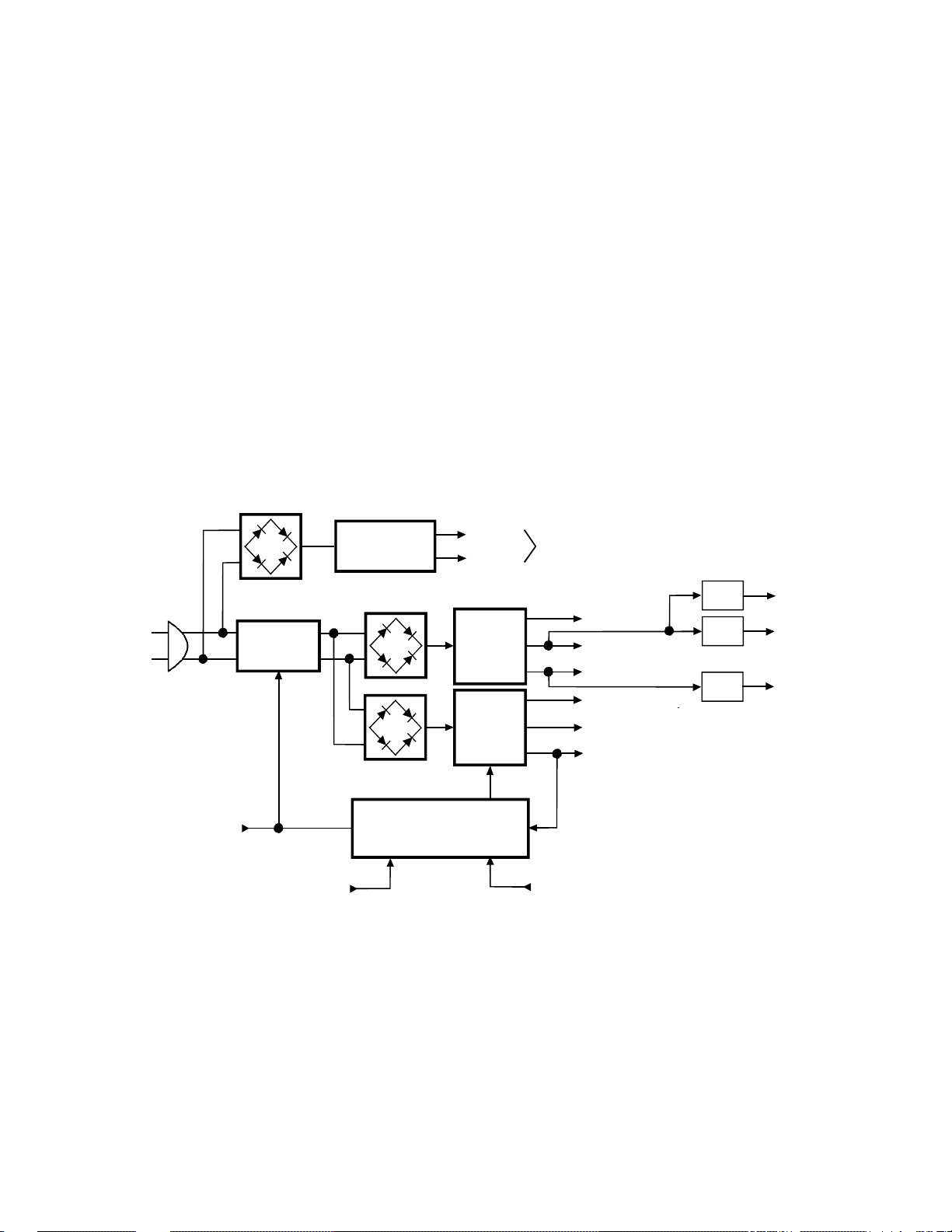
The E model PTVs actually have three separate power
supplies as shown in Figure 1-9. These supplies consist of
the Standby Supply, the Main Switch Mode Supply, and
the Sub Switch Mode Supply. The Standby Supply provides
the 5 VDC needed to run the microcomputer and the
customer interface controls, such as the key pad and the IR
receiver. When the set is turned on, the switch closes to
activate the two switch mode supplies and provide the
numerous DC voltages needed to operate the set.
STANDBY
REGULATOR
The Control/Protection circuit, Z801, has two functions.
The first is to regulate the Main Switch Mode Supply, and
the second is to monitor over current, over voltage, and
under voltage sensors throughout the set. If any one of
these sensors activates the protection circuit, Z801 turns
off the switch powering the two switch mode supplies thus
turning off the set. If this occurs, a red LED on the front
panel flashes at half second intervals, and the set must be
unplugged to reset Z801.
+5VDC
RESET
TO MICROCO MPUTER
120VAC
POWER
ON/OFF FROM
MICROCOMPUTER
SWITCH
POWER
OFF
X-RAY SENSING
Figure 1-9 Power Supply/Protection Block Diagram
SWITCH
SWITCH
FEEDBAC K
Z801
16
CONTROL/PRO TEC TION
13
MODE
(SUB)
MODE
(MAIN)
3
14
+30VDC
+15VDC
-15VDC
+12VDC
+38VDC
+125VDC
1
OVERCURRENT,
OVERVOLT A GE, &
UNDER VOLTAGE
SENSING
REG
REG
REG
+5VDC
+15VDC
-9VDC
1-12
Page 18
11. HORIZONTAL AND VERTICAL DEFLECTION
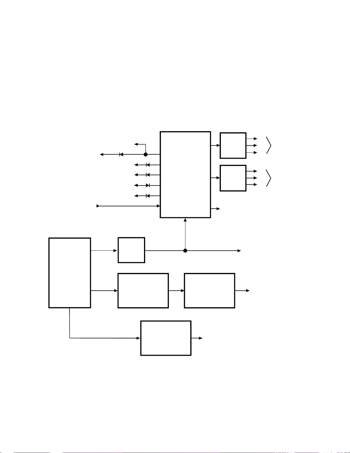
Deflection circuitry in the E model PTV’s is rather straight
forward as show in Figure 1-10. The horizontal pulse from
Q501 drives the horizontal drive circuitry, which in turn
drives the Horizontal Yokes and the Flyback Transformer,
T461. Numerous low voltage DC supplies are produced by
the Flyback, as well as the high voltages for the anode,
focus, and screen drives. To prevent excessive high
voltages, a sample X-Ray protection voltage is monitored
by the over voltage protection circuits.
AC TO HEATERS
+23VDC TO X-RAY
PROTECT
+12VDC
+35VDC
-27VDC
+200VDC
+125VDC FROM
MAIN POWER
9
TRANSFORMER
7
6
5
3
2
Vertical drive (VD) is applied to the DPC circuit, U421, to
correct any distortions before it’s sent to the Vertical Drive
circuit, Q301. Then the vertical drive circuit supplies the
signals required by the yokes for deflection.
To enhance horizontal transitions between dark and light
areas of the picture, a Velocity Scan Modulation (VSM)
signal is produced by Q501. This signal is sent to the SVM
circuit, E036Z, which in turn drives the SVM coils on the
CRTs.
R
T461
HV
HV
DIST
BLOCK
G
B
30.7KV
TO CRT
ANODES
FLYBACK
2
8
FOCUS
BLOCK
TO ABL
R
G
B
FOCUS &
SCREEN DRIVE
TO CRTs
CIRCUIT
Q501
VIDEO
CHROMA
DEFLECTION
PROCESSING
48
VSM
1
HORIZ
DRIVE
H-OUT
23
VD
31
4
HORIZ
DRIVE
U421
DPC
CIRCUIT
2
6
EO36Z
SVM
4
Q301
VERTICAL
DRIVE
1
TO SVM
COILS
CIRCUIT
Figure 1-10 Horizontal and Vertical Deflection Block Diagram
TO HORIZ
YOKES
TO VERT
2
YOKES
1-13
Page 19
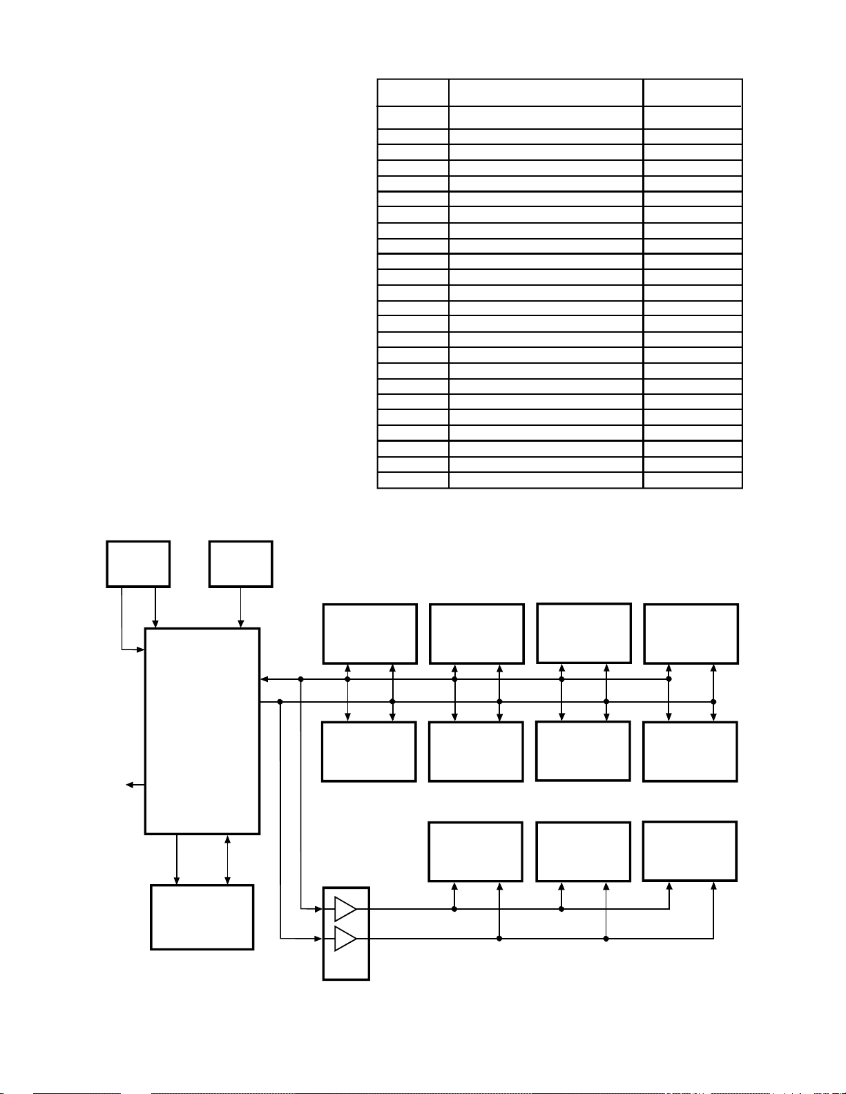
12. I2C Communications
REG
ADJUSTMENT
PRESET
The TG-1 chassis uses I2C data communications to
control all customer features and most of the service
adjustments that where previously done with discrete
devices, refer to Figure 1-11. All communications
are controlled by the Microcomputer, QA01 through
serial data lines (SDA) and serial clock lines (SCL).
Memory settings for customer controls and service
adjustments (except convergence data) are stored in
the E2PROM Memory, QA02, and communicated
to QA01 by the SCL0 and SDA0 lines. Data and
clock lines SDA1 and SCL1 communicate with
most of the circuits in the set. However, there are
three plug in circuits where the data and clock
signals are buffered by QB90 to provide isolation.
All customer functions and most services
adjustments are implemented through the Key Pad
and the Remote Sensor. The RMT OUT signal on
the microcomputer drives the IR Transmitter on the
front panel, but it’s only used in the manufacturing
process. Figure 1-12 shows the Service Registers
and their default values used for making adjustments
in the set.
RCUT RED CUTOFF 40
G C U T G R E E N C U T O F F 4 0
B C U T B L U E C U T O F F 4 0
R D R V R E D D R I V E 4 0
B D R V B L U E D R I V E 4 0
C N T X S U B - C O N T R A S T M A X 7 F
B R T C S U B - B R I G H T C E N T E R 8 0
COLC SUB-COLOR CENTER 50
TNTC SUB-TINT CENTER 40
SCOL SAP-COLOR 15
SCNT SUB-CONTRAST 15
HPOS HORIZ. POSITION 16
VPOS VERTICAL POSITION 00
HIT VERTICAL HEIGHT D1
GMPS GMPS 00
VLIN VERTICAL LINEARITY 12
VSC A-S CORRECTION 08
V P S V E R T I C A L S H I F T 1 5
VCP V-COMPENSATION 03
WID PICTURE WIDTH 25
TRAP TRAPEZIUM 10
HCP H-COMPENSATION 02
VFC V-F CORRECTION 0F
STRH HORIZ. START POSITION 82
Figure 1-12 Service Register Default Values
KEY A
TO IR
LED
TRANS
KEY
PAD
KEY B
18 35
17
REMOTE
SENSOR
QA01
MICRO-
COMPUTER
RMT OUT
3
12
SCL0 SDA0
11
65
QA02
EEPROM
MEMORY
38
SDA1
SCL1
37
IC501
V/C/D
PROCESSING
27 28 21
910
COMB FILTER
OR
3D-Y/C
3
2
QB90
SDA2
5
SCL2
6
H002
IF/MTS/A.PRO
20
25
QAV01
SWITCHING
F. SURR.,
DSP/DOLBY,
D. PRO LOGIC
14 15 14 13
24 44
AV
DPC CIRCUIT
CIRCUIT
H001
TUNER
U421
ZY01
PIP
21
HY01
TUNER/IF
34
43
Q701
CONV.
PROCESSOR
UM01
EDS/CC
RGB SW.
14 13
Figure 1-11 I2C Communication Block Diagram
1-14
Page 20
13. Digital Convergence
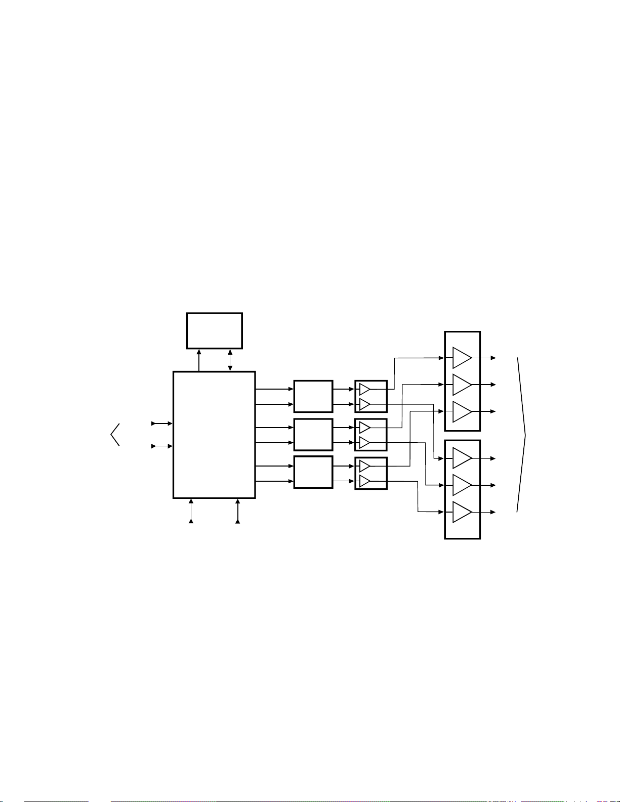
The TG-1 model PTV’s are equipped with a new digital
convergence circuit shown in Figure 1-13. This circuit
allows servicers to set the convergence with the remote
control. Q701, the Digital Convergence Processor aligns
the convergence from data received from the remote, and
saves the settings in the E2PROM, Q713. The digital
convergence signals are converted to analog by the D/A
Converters Q703, Q704, and Q705. Then they are amplified
Q713
EEPROM
FROM
QAO1
CLK
DATA
65
CLK
45
Q701
43
DIGITAL
CONVERGENCE
44
PROCESSOR
31 32
HD
FROM
IC501
46
VD
FROM
Q301
DATA
7
RH
86
6
RV
87
GH
89
GV
90
BH
96
BV
97
7
6
7
6
CONV.
CONV.
CONV.
by the pre amps (Q715, Q717, & Q719) and power amps
(Q751 & Q751) before being applied to the convergence
yokes. The Power Amps Q752 and Q751 dissipate allot of
heat because of their current draw, so the supplies to these
amps have a number of sensors for over current conditions.
Most of the convergence circuit is on a shielded board, but
the power amps are easily accessible for service.
Q752
18
11
9
18
11
9
Q703
D/A
Q704
D/A
Q705
D/A
15
20
Q715
Q717
Q719
1
7
1
7
7
1
3
1
5
20
3
1
5
20
5
1
3
14
6
15
14
6
Q751
RH
GH
BH
TO
CONV.
YOKES
RV
GV
BV
Figure 1-13 Convergence Block Diagram
1-15
Page 21

LAB 1
BASIC OPERATION AND UNIT UNDERSTANDING
As a servicer, it is important now, more than ever, to fully understand the operation and functions of
a television set before proceeding with a repair. This is because many of the problems encountered by
a customer today can be caused by an incorrect menu selection or improper setup.
Therefore, the purpose of this lab is to familiarize you with menus and features of the television from
the customer’s point of view.
SECTION ONE
BASIC OPERATION
1. Verify that the unit is connected to an AC supply, and that a signal is connected to the ANT 1
input. While verifying signal connections, take time to examine all of the inputs on the rear and
front (behind door) of the unit.
2. Turn on the set with the remote control and tune to an active channel. Refer to page 9 of the
service manual provided and familiarize yourself with all of the keys on the remote paying,
particular attention to the following keys:
o EDS
o TIMER
o PIP Functions
Open the bottom door on the remote control by sliding it down. Try each key starting with the upper
row. Each of these buttons brings up another menu and/or sub-menus.
3. In the Picture Menu, What is Color Temperature?
____________________________________________________________________________
____________________________________________________________________________
4. In the Audio Menu, Where can the speakers be turned off by the user?
____________________________________________________________________________
____________________________________________________________________________
5. In the Setup Menu, What is Favorite Channel?, What is Channel Lock?
____________________________________________________________________________
____________________________________________________________________________
1-16
Page 22

6. Refer to page 16 of the Service Manual and perform the User Convergence Adjustments. How
is this different from previous Toshiba PJTVs?
____________________________________________________________________________
____________________________________________________________________________
7. In the Option Menu , How many different languages are there? What are they used for? What is
Channel Label Used for?
____________________________________________________________________________
____________________________________________________________________________
____________________________________________________________________________
____________________________________________________________________________
NOTES:
____________________________________________________________________________
____________________________________________________________________________
____________________________________________________________________________
____________________________________________________________________________
____________________________________________________________________________
____________________________________________________________________________
SECTION TWO
DISASSEMBLY & SERVICE POSITION
Follow the procedure listed below to gain access to the tubes and circuit boards.
1. Remove the speaker grill by holding the sides and pulling straight out.
2. Take out the four screws holding the plastic shield in place. Then remove the shield.
3. Remove the control wires from the holder on the metal shield in front of the CRTs.
4. Remove the 4 screws holding the metal shield in place. The shield is notched, so slide it to the
right then down to remove it.
5. Remove the two screws holding the front control panel. Then release the tabs on either side and
let it hang down out of the way.
6. Remove the 4 screws holding the bottom of the screen. Then lift up on the top of the screen and
pull it away from the cabinet.
1-17
Page 23

7. Remove the 5 screws holding the back panel. Then remove the back panel.
8. Reattach the control panel to the light box.
9. Remove the six screws on the front of the light box.
10. Remove the three screws on the back of the cabinet.
11. Remove the one screw holding the back of the light box to the cabinet.
12. From the front of the set, lift the light box up just a little, and pull it towards you.
13. Pull the light box all the way out of the cabinet and turn it on its side.
CAUTION: the light box weighs about 85 pounds, so get help if you need it.
SECTION THREE
IDENTIFICATION
1. Identify each of the board assemblies and note their locations. Use Figure 1-5 to help you
identify the various boards.
o Convergence/Output/Power Board
o Deflection/Power Board
o Main PCB
o Front Surround Board
o Digital Comb Filter Board
o PIP Board
o EDS/CC Board
2. Is there a convergence board in this unit?
If so, where?
____________________________________________________________________________
____________________________________________________________________________
3. How does this convergence setup differ from previous models?
____________________________________________________________________________
____________________________________________________________________________
4. Examine the Flyback and HV lead assemblies. What is different about this area from earlier
models?
____________________________________________________________________________
____________________________________________________________________________
1-18
Page 24

5. Is it possible for one technician to perform a service call on this type of unit?
____________________________________________________________________________
____________________________________________________________________________
6. Put the lightbox in the cabinet, but don't screw it in. Then replace the screen and control panel.
Use a few screws to hold the screen and control panel in place.
SUMMARY
In this lab, the operation and function of the unit was determined, and the unit was set up for service
on the bench. Common user type problems in addition to overall serviceability was also discussed.
END OF LAB 1
1-19
Page 25

LAB 2
TEST SIGNALS, SELF DIAGNOSTICS, & SERVICE REGISTERS
OBJECTIVES: After completing this lab you will be able to:
1. Enter and exit the set’s internal video and audio test signals.
2. Use the test signals for troubleshooting.
3. Use the set’s self diagnostic feature.
4. Make adjustments in the set with the service registers via the remote control.
SECTION ONE
VIDEO TEST SIGNALS
1. Verify that the unit is connected to an AC supply, and that a signal is connected to the ANT 1
input.
2. Enter the service mode by pressing mute on the remote. Press and hold mute a second time
while pressing menu on the control panel. An S appears in the upper right corner of the screen
indicating that the set is in the service mode. Press menu and the RCUT register appears in the
upper left corner of the screen.
3. Push the TV/VIDEO button on the remote once to enter the internal test pattern mode. The
screen should be red.
4. Slowly cycle through the test signals with the TV/VIDEO button until the white cross hairs on
a black background appear. (If the TV/VIDEO button is pushed in rapid succession, the set will
jump out of the test signal mode to one of the inputs - ANT 1, VIDEO 1, VIDEO 2, or VIDEO
3. The set is still in the service mode, so if this occurs, push the menu button then the TV/
VIDEO button to get back into the test signal mode.)
5. Plug a video cable into the VIDEO 1 input jack (make sure the other end of the cable is not
plugged into a video source)
6. What happened to the cross hairs?
____________________________________________________________________________
____________________________________________________________________________
7. If something did happen to the cross hairs, why did it happen?
____________________________________________________________________________
____________________________________________________________________________
1-20
Page 26

8. Is there video on the screen?
____________________________________________________________________________
____________________________________________________________________________
9. If there is video on the screen, where does it come from?
____________________________________________________________________________
____________________________________________________________________________
10. Unplug the video cable.
SECTION TWO
AUDIO TEST SIGNALS
1. Push the 8 button on the remote to activate the audio test signal. (NOTE: The internal test
pattern mode must be activated for this feature to work.)
2. Push the mute button twice. Now you can control the volume of the signal.
3. Select AUD on the remote control.
4. Select BALANCE and adjust it from left to right with the + and - buttons.
5. Select SPEAKERS and turn them off then on. (NOTE: The speakers are turned off at Q601,
refer to Figure 1-8, while the volume, bass, treble, and balance are controlled in H002. This
means you can troubleshoot most of the audio system with the speakers off.)
6. Plug an audio cable into the left AUDIO 1 input jack (make sure the other end of the cable is
not plugged into an audio source)
7. What happened to audio?
____________________________________________________________________________
____________________________________________________________________________
8. If something did happen to the audio, why did it happen?
____________________________________________________________________________
____________________________________________________________________________
9. Push the 8 button to turn off the audio test signal.
10. Cycle the video test signals back to the ANT 1 signal with the TV/VIDEO button.
1-21
Page 27

SECTION THREE
SELF DIAGNOSTICS
1. Push the 9 button to activate the self diagnostic feature.
2. What does POWER indicate?
____________________________________________________________________________
____________________________________________________________________________
3. What does BUS LINE indicate?
____________________________________________________________________________
____________________________________________________________________________
4. What does BUS CONT indicate?
____________________________________________________________________________
____________________________________________________________________________
5. What does BLOCK indicate?
____________________________________________________________________________
____________________________________________________________________________
6. Push the EXIT button to exit the self diagnostic feature.
7. Select the VIDEO 1 input with the TV/VIDEO button. (Make sure there is no signal applied to
VIDEO 1)
8. Push MENU on the control panel to display the registers.
9. Push 9 to activate the self diagnostic feature.
10. Is the display different from the previous display. ______
11. If it is, explain why.
____________________________________________________________________________
____________________________________________________________________________
12. Push the EXIT button to exit the self diagnostic feature.
13. Push MENU on the control panel to display the registers.
1-22
Page 28
SECTION FOUR
SERVICE REGISTERS
NOTE: In each of the following exercises write down the register’s value before adjusting it. Then
restore the register to its original value before proceeding to the next exercise.
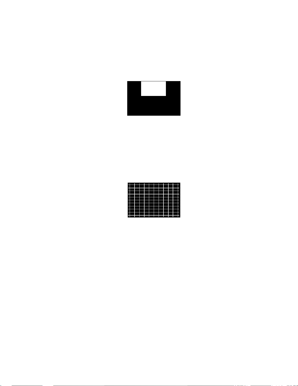
1. Enter the internal test pattern mode and select the test signal that has a white window in the
upper center of a black background as shown below.
2. Increase the RCUT register value and describe its effect on the picture.
RCUT______
____________________________________________________________________________
____________________________________________________________________________
3. Change the test signal to the white on black cross hatch pattern as shown below.
4. Select the HPOS register and vary its value between 00 and 1F. Describe its effect on the
picture. What happens if you increase the register to 20?
HPOS______
____________________________________________________________________________
____________________________________________________________________________
5. Select the VPOS register and vary its value between 00 and 07. Describe its effect on the
picture. What happens if you increase the register to 08?
VPOS______
____________________________________________________________________________
____________________________________________________________________________
1-23
Page 29

6. Select the HIT register and vary its value 5 steps above and below the recorded value.
Describe its effect on the picture.
HIT______
___________________________________________________________________________
____________________________________________________________________________
7. Select the VLIN register and vary its value 8 steps above and below the recorded value.
Describe its effect on the picture.
VLIN______
___________________________________________________________________________
____________________________________________________________________________
8. Select the WID register and vary its value 8 steps above and below the recorded value.
Describe its effect on the picture.
WID______
___________________________________________________________________________
____________________________________________________________________________
9. Select the STRH register and vary its value 8 steps above and below the recorded value.
Describe its effect on the picture.
STRH______
___________________________________________________________________________
____________________________________________________________________________
SUMMARY
Now that you have completed Lab 2, you should be able to use the internal video and audio test
signals, the self diagnostic feature, and the service registers for making adjustments.
END OF LAB 2
1-24
Page 30

SECTION II
TUNER, IF/MTS/S.PRO MODULE
2-1
Page 31
1. CIRCUIT BLOCK
H002 - IF/MTS/A.PRO Module MVUS34S
EL466L
H001
Main Tuner
RF AGC
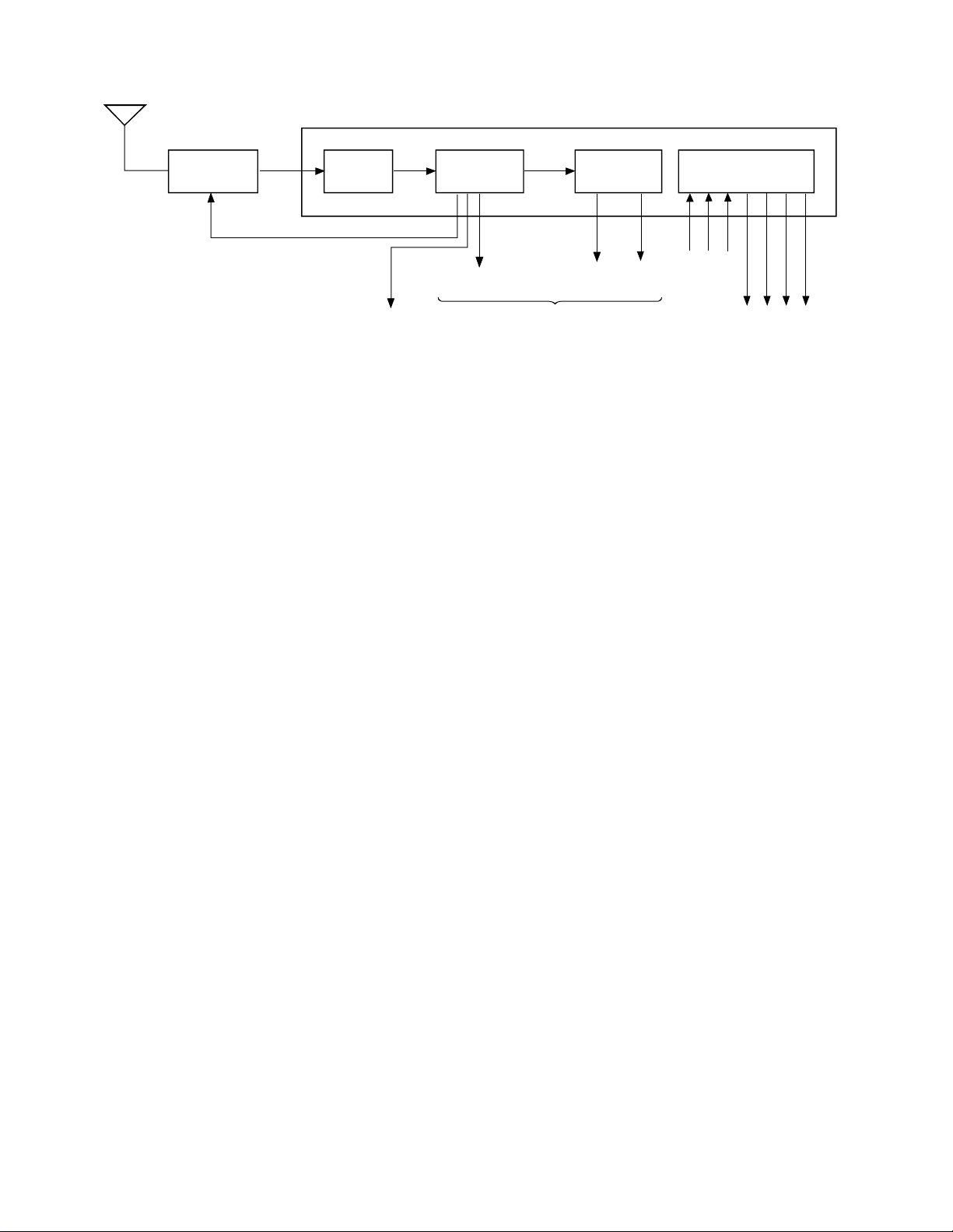
1-1. Outline
(1) RF signals sent from an antenna are converted into
intermediate frequency band signals (video: 45.75 MHz,
audio: 41.25 MHz) in the tuner. (Hereafter, these signals
are called IF signals.)
(2) The IF signals are band-limited in passing through a
SAW filter.
(3) The IF signals band-limited are detected in the VIF
circuit to develop video and AFT signals.
(4) The band-limited IF signals are detected in the SIF
circuit and the detected output is demodulated by the
audio multiplexer, developing R and L channel outputs.
These outputs are fed to the A/V switch circuit.
(5) A sound processor (S.PRO.) is provided.
SAW
Filter
AFT output
Fig. 2-1 Block diagram
SIF
VIF/SIF
Circuit
TP12
Video output
To A/V switch circuit
output
Sound
Multiplex
Circuit
TV
R-OUTTVL-OUT
C-IN
A.PRO Circuit
R-IN L-IN
R-OUT
L-OUT
(5) VIF/SIF circuit uses PLL sync detection system to
improve performances shown below:
• Telop buzz in video over modulation
• DP, DG characteristics (video high-fidelity
reproduction)
• Cross color characteristic (coloring phenomenon at
color less high frequency signal objects)
(6) HIC SBX1637A-22 is used in the audio multiplexer
circuit to minimize the size with increased performance.
(7) As a sound control processor, TA1217N is used. I2C-
bus data control the DAC inside the IC to perform
switching of the audio multiplexer modes.
(L+R)
-OUT
C-OUT
1-2. Major Features
(1) The VIF/SIF circuit is fabricated into a small module
by using chip parts considerably.
(2) As the tuner, EL466L that which contains an integrated
PLL circuit is employed.
(3) Wide band double SAW filter F1802R used.
(4) FS (frequency synthesizer) type channel selection system
employed.
2-2
Page 32
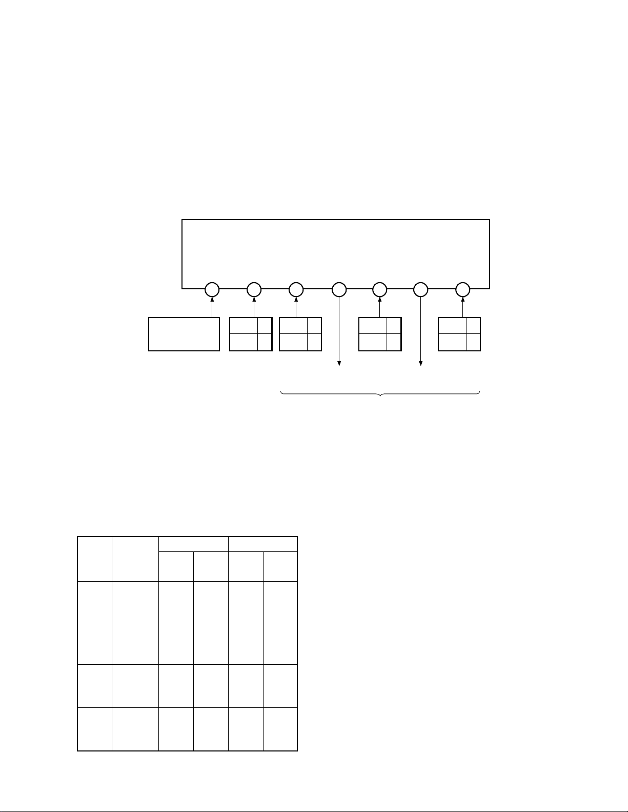
1-3. Audio Multiplex Demodulation Circuit
The sound multiplex composite signal FM-detected in the
PIF circuit enters pin 12 of HIC (hybrid IC) in passing
through the separation adjustment VR RV2 and amplified.
After the amplification, the signal is split into two: one enters
a de-emphasis circuit, and only the main signal with the L-R
signal and a SAP signal removed enters the matrix circuit. At
the same time, the other passes through various filters and
trap circuits, and the L-R signal is AM-demodulated, and the
SAP is FM-demodulated.
MVUS34S
Then, both are fed to the matrix circuit. At the same time,
each of the stereo pilot signal fH and the SAP pilot signal 5fH
is also demodulated to obtain an identification voltage. With
the identification voltage thus obtained and the user control
voltage are used to control the matrix.
The audio signals obtained by demodulating the sound
multiplex signal develop at pin 10 and 11 of HIC and develop
the terminals of 12 and 14 of the module.
MPX
Out
11
SAP 0V
Other 5V
TV waveform detection
Monitor the input
pin for multiplex
sound IC
9
10
Stereo 0V
Other 5V
Fig. 2-2 Block diagram of MVUS34S
Table 2-1 Matrix for broadcasting conditions and
reception mode
Output OSD display
Broad- Switching
casted mode
12 pin 14 pin
(R) (L)
Stereo SAP
Stereo STE R L Y N
SAP R L Y N
MONO L+R L+R Y N
Mono STE L+ R L+R N N
SAP L+R L+R N N
MONO L+R L+R N N
Stereo STE R L Y Y
+ SAP SAP SAP Y Y
SAP MONO L +R L+R Y Y
Mono STE L+ R L+R N Y
+ SAP SAP SAP N Y
SAP MONO L +R L+R N Y
TV
R-Out
output (R)
DAC-out1
(SURR ON/OFF)
12 13 14
OFF 0V
ON 9V
To AV select circuit
TV waveform detection
TV
L-Out
output (L)
DAC-out2
(RFSW)
15
RF1 0V
RF2 9V
Note:
Of the mode selection voltages, switching voltages for STE,
SAP, MONO do not output outside the module.
They are used inside the module to control the BUS.
2-3
Page 33
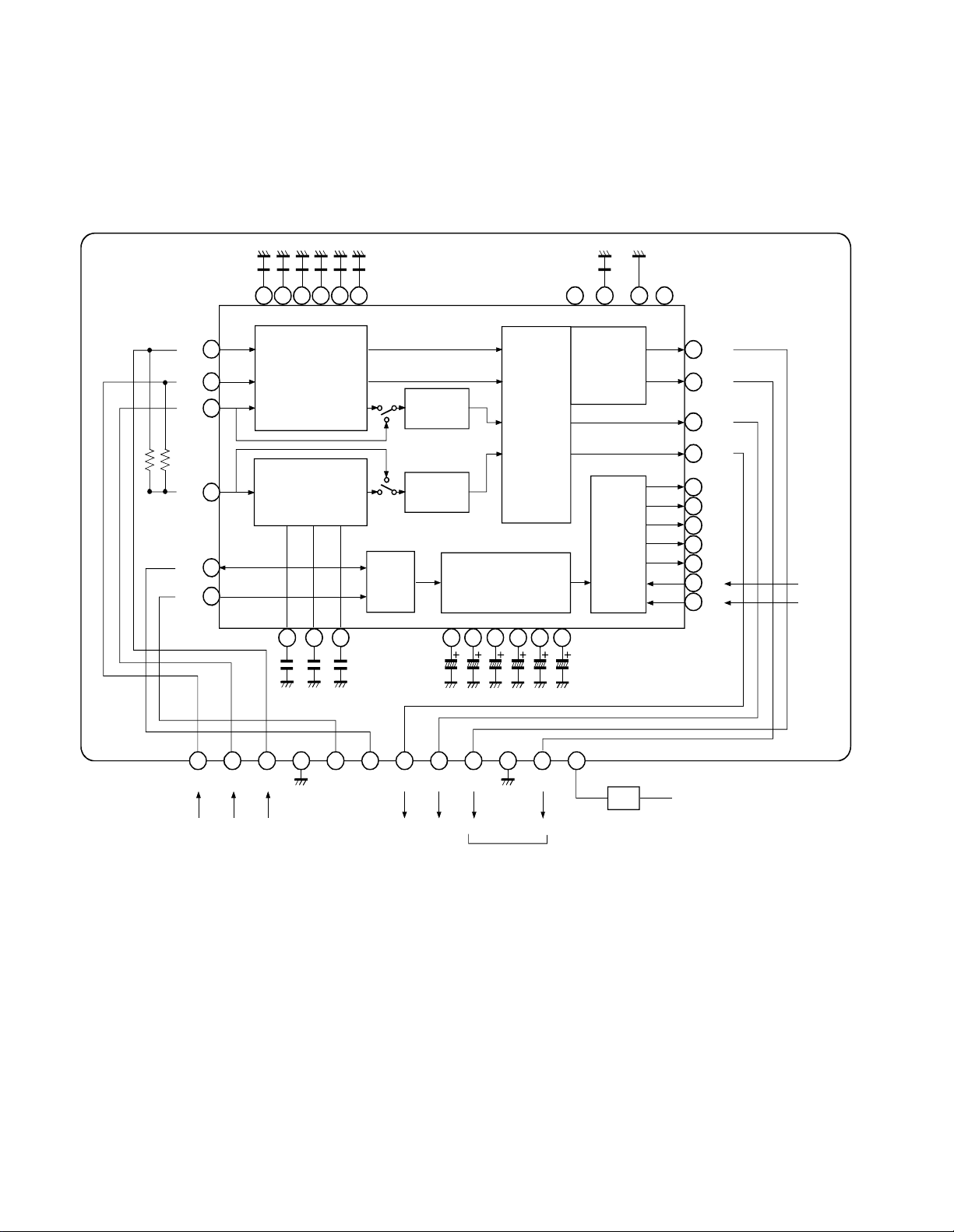
1-4. A.PRO Section (Audio Processor)
The S.PRO section has following functions.
(1) Woofer processing (L+R output)
(2) High band, low band, balance control
(3) Sound volume control, cyclone level control
(4) Cyclone ON/OFF
TA1217N
All these processing are carried out according to the BUS
signals sent from a microcomputer.
Fig. 2-3 shows a block diagram of the A.PRO IC.
Lin
Rin
Cin
Win
SDA
SCL
1272922 32
34
30
2
3
20
21
TONE CONTROL
LPF
456 7
36
2
I C
Center
LEVEL
Woofer
LEVEL
31 24
D/A
CONV
VOLUME
23
22 19
30 9
BALANCE
I/O
28
8
L out
26
R out
25
C out
18
W out
10
17
16
15
14
13
12
11
SAP Ident.
STE Ident.
16
R-in C-in L-in
From From From
A/V Dolby A/V
18 19 20 21 22
17
24
23
SCL1 SDA1 W-out C-out L-out R-out
to Q601 to Q641 to Q601 to Q601
SBS
Via QS101
26 27
25
Fig. 2-3 A.PRO block diagram
2-4
9V
Page 34
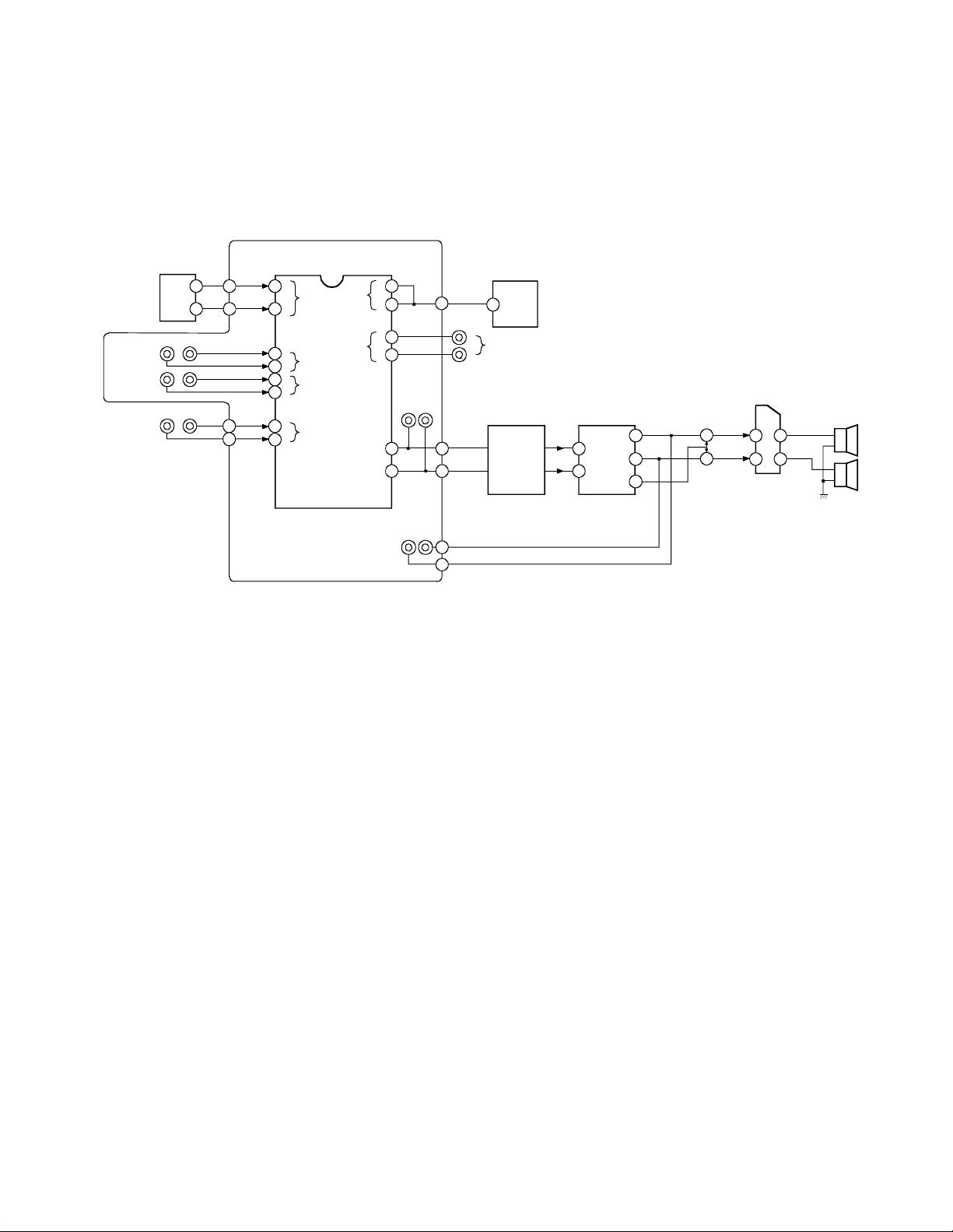
Configuration of the audio circuit and signal flow are given
in Fig. 2-4
A/V PCB
VIF+MTS+S.PRO
VIDEO 1
VIDEO 2
VIDEO 3
(FR ONT IN P U T )
MODULE
R
L
R L
R L
R L
12
EQ
14
ER
AF
AG
QV01
R
6
From
From PIP
Main
L
Tuner
5
VIDEO 1
VIDEO 2
VIDEO 3
OUTPUT
L
11
13
R
8
L
9
R
L
15
17
R
Tuner
29
L
VIDEO
OUTPUT
TERM IN AL
EN
AS
AR
R
31
2
L
PIP
1
R
35
R
37
L
FOR PIP
IF MODULE
L
PIP OUT
(AUDIO)
R
CIRCUIT
AUDIO
DSP
TP48E90 ONLY
VIF+MTS+A.PRO
MODULE
R OUT
16
R
18
L
W OUT
L OU T
Q601
26
24
22
R
+
+
2511
L
7
R
L
VARIABLE
AUDIO OUTPUT
TERM INAL
RL
AI
AJ
Fig. 2-4
2-5
Page 35
2. PIP TUNER
TUNER
SECTION
RF AGC
SAW
FILTER
VIF/SIF
CIRCUIT
Lable
Name
Lot No.
AFT
OUTPUT
VIDEO
OUTPUT
AUDIO
OUTPUT
Fig. 2-5
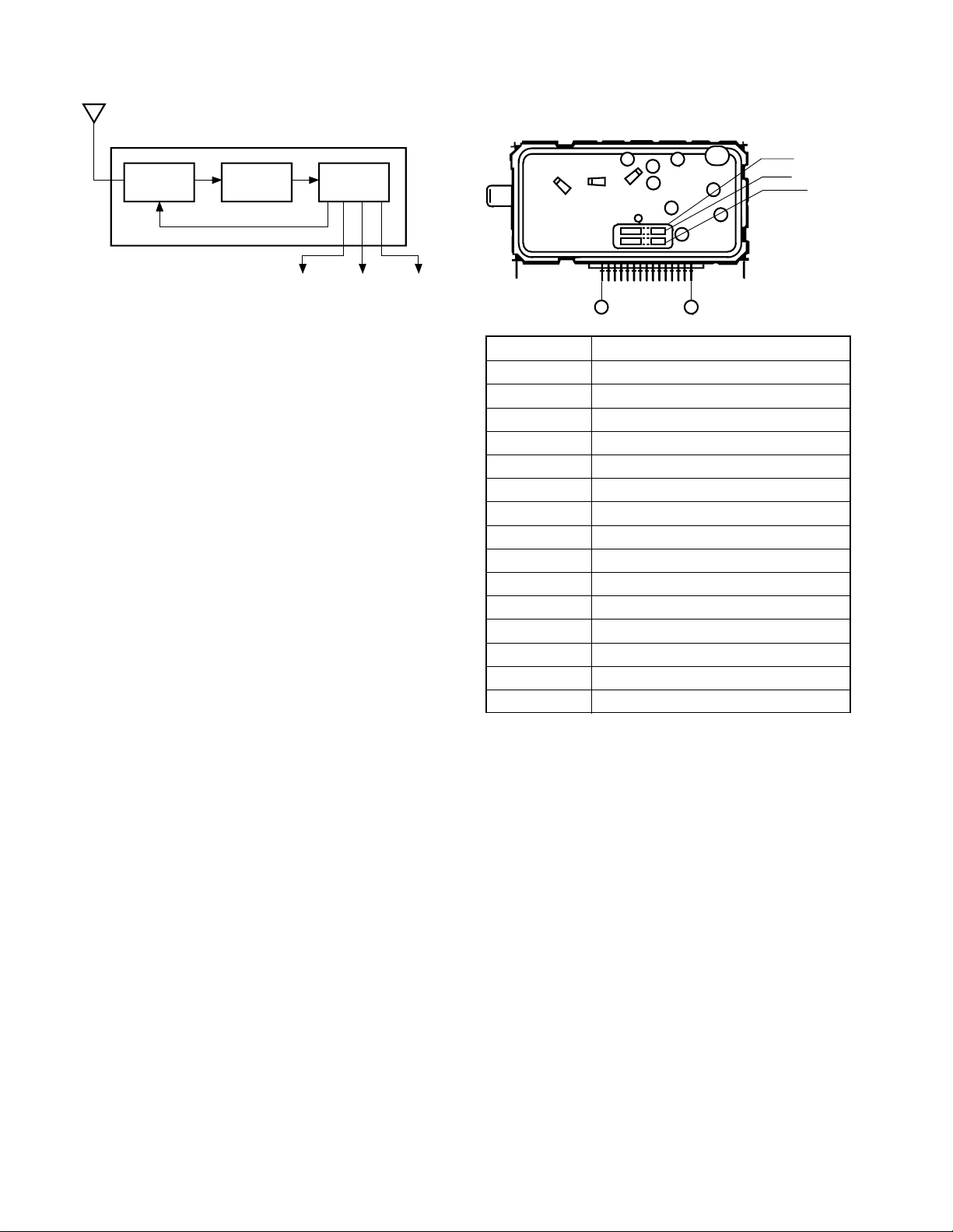
2-1. Outline
The PIP tuner (EL922L) consists of a tuner and an IF block
integrated into one unit. The tuner receives RF signals
induced on an antenna and develops an AFT output, video
output, and audio output.
The tuner has receive channels of 181 as in the tuner for the
main screen and it is also controlled through the I2C-bus.
As the IC for the IF, a PLL complete sync detection plus
audio inter carrier system are employed.
1
15
Terminal No. Name
1NC
2 32V
3 S-CLOCK
4 S-DATA
5NC
6 ADDRESS
75V
8 RF AGC
99V
10 AUDIO
11 GND
12 AFT
13 NC
14 GND
15 VIDEO
Fig. 2-6 Tuner terminal layout
2-6
Page 36

SECTION III
CHANNEL SELECTION CIRCUIT
3-1
Page 37

1. OUTLINE OF CHANNEL SELECTION CIRCUIT SYSTEM
The channel selection circuit in the N5SS chassis employs a
bus system which performs central control by connecting
a channel selection microcomputer to a control IC in each
circuit block through control lines called a bus. This bus
system herin referred to as the I2C bus system (two line bus)
is licensed from and was developed by Philips.
Integrated circuits controlled by the I2C bus system are :
QN06 for audio signal processing, Q501 for V/C/D signal
processing , QV01 for A/V switching, QA02 for non
volatile memory, main and sub U/V tuners (H001, HY01),
Q302 for deflection distortion correction, QY04 for PIP
signal processing, QM01 for DSP, and Q701 for closed
caption control.
Differences from the previous N5SS chassis include;
1. On-screen display generation now originates within
ICA01. A separate IC is no longer used.
2. The microcomputer does not perform the closed
caption function, but instead controls a separate IC
for this purpose.
3. The system uses two sperate channels of I2C bus. One
of these is dedicated for communication with the
non-volatile memory.
2. OPERATION OF CHANNEL
SELECTION CIRCUIT
• Setting of memory values for video parameters
such as white balance (RGB cutoff, GB drive) and
gcorrection, etc.
• Setting of video parameters of video modes
(Standard, Movie, Memory)
(3) CONTROL OF A/V SWITCH IC (QV01 Toshiba
TA1218N)
• Preforms source switching for main screen and
sub screen
• Performs source switching for TV and up to three
video inputs
(4) CONTROL OF NON-VOLATILE MEMORY IC
(QA02 Microchip 24LC08BI/P)
• Memorizes data for video and audio signal
adjustment values, volume and woofer adjustment
values, external input status, etc.
• Memorizes adjustment data for white balance
(RGB cutoff, GB drive), sub-brightness, sub color,
sub tint, etc.
• Memorizes deflection distortion correction value
data adjusted for each unit.
(5) CONTROL OF U/V TUNER UNIT (H001 Matsushita
EL466L, HY01 Toshiba EL922L)
• A desired channel can be tuned by transferring a
channel selection frequency data (divided ratio
data) to the I2C bus type frequency synthesizer
equipped in the tuner, and by setting a band
switch which selects the UHF or VHF band.
An 8 bit, Toshiba microcomputer (series TLCS-870) is
used within the television as ICA01. Part number
TMP87CS38N-3152 or similar is employed.
With this microcomputer, each IC and circuit shown below
are controlled.
(1) CONTROL OF AUDIO SIGNAL PROCESS IC (QN06
Toshiba TA1217N)
• Adjustments for volume, treble, bass and balance
• Selection between surround mode and DSP mode,
and level adjustment
• Level adjustment of BAZOOKA (Sub-Bass)
system
• Audio muting during channel selection or no signal
reception.
(2) CONTROL OF VIDEO/CHROMA/DEF SIGNAL
PROCESS IC (Q501 Toshiba TA1222N)
• Adjustments for uni-color, brightness, tint, color
gain, sharpness and PIP uni-color
• Setting of adjustment memory values for subbrightness, sub-color and sub-tint, etc.
(6) CONTROL OF DEFLECTION DISTORTION
CORRECTION IC (Q302 Toshiba TA8859P)
• Sets adjustment memory value for vertical
amplitude, linearity, horizontal amplitude,
parabola, corner, trapezoid distortion.
(7) CONTROL OF PIP SIGNAL PROCESS IC (QY04
Toshiba TC9083F)
• Controls ON/OFF and position shift of PIP.
(8) CONTROL OF DIGITAL SOUND PROCESSOR IC
(QM04 Yamaha YSS238-D)
• Performs mode switching of DSP.
(9) CONTROL OF CLOSED CAPTION/EDS (QM01
Motorola XC144144P)
• Controls Closed Caption/EDS.
3-2
Page 38
3. MICROCOMPUTER
SDA
SCL
1 - 7
8
9
1 - 7
8
9
1 - 7
8
9
Start
condition
Stop
condition
Address
R/W
Ack Data
Ack
DATA Ack
Approx.180mS
Some device may have no data,
or may have data with several
bytes continuing.
The main Microcomputer TMP87CS38N-3152 has 60k
byte of ROM capacity and is equipped with an internal OSD
function.
The specification is as follow.
• Type name : TMP87CS38N-3152
• ROM : 60k byte
• RAM : 2k byte
• Processing speed : 0.5m s (at 8MHz with Shortest
command)
• Package : 42 pin shrink DIP
•I2C-BUS : two channels
• PWM : 14 bit x 1, 7 bit x 9
• ADC : 8 bit x 6 (Successive comparison system,
Conversion time 20ms)
• OSD
Character kinds : 256
Character display : 24 characters x 12 lines
Character dot : 14 x 18 dots
Character size : 3 kinds (Selected by line)
Character color : 8 colors (Selected by character)
Display position : Horizontal 128 steps, Vertical
256 steps
This microcomputer performs the functions of an Analog to
Digital converter, reception of U/V TV and OSD display in
one chip.
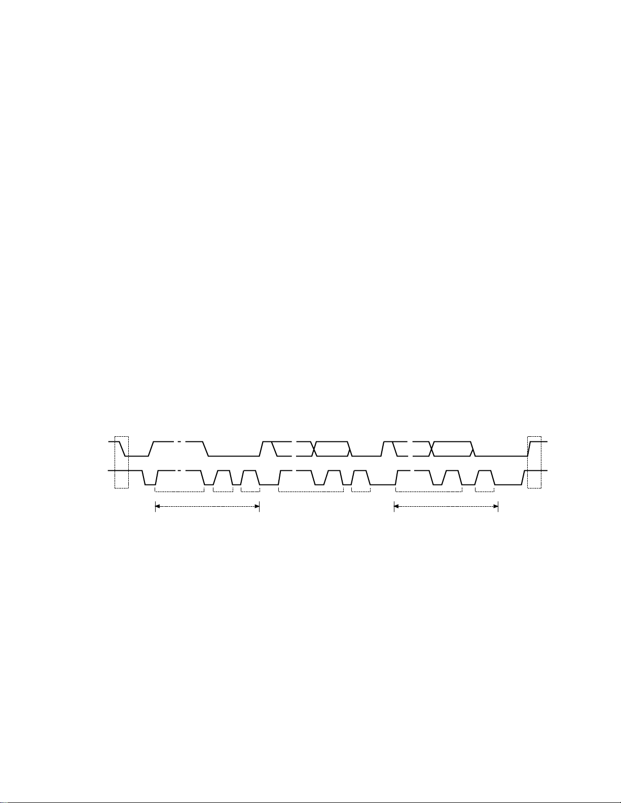
IIC device controls through I2C bus. (Timing chart : See fig.
3-1)
• Pin 8, (LED) is used to source current and is an output
only.
• For clock oscillation, an 8MHz ceramic oscillator is
used.
•I2C has two channels. One is for EEPROM only.
• A Self diagnosis function which utilizes the ACK
function of I2C is employed
• Function indication is added to service mode.
• Operation by remote control is possible, and controls
and adjustments can be made with no physical contact
is possible. (Bus connector in the conventional bus
chassis is deleted.)
• Substantial self diagnosis function
(1) B/W composite video signal generating function
(inside micon, green crossbar added)
(2) Generating function of audio signal equivalent
to 1kHz (inside micon)
(3) Detecting function of power protection circuit
operation
(4) Detecting function of abnormality in I2C bus
line
(5) Functions of LED blink indication and OSD
indication
(6) Block diagnosis function which uses new VCD
and AV SW
Fig. 3-1
3-3
Page 39
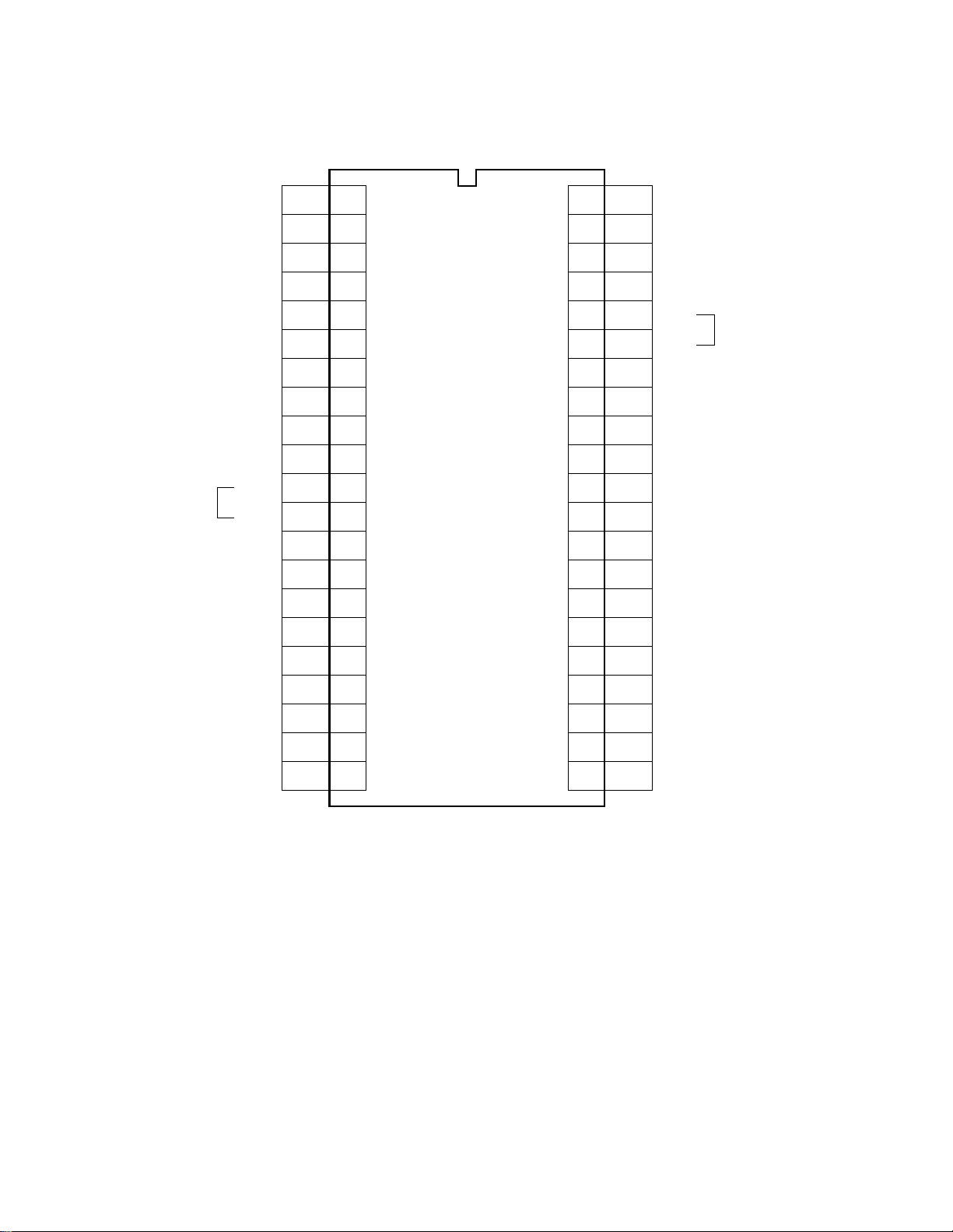
4. MICROCOMPUTER TERMINAL FUNCTION
S
TMP87CS38N3152 (QA01)
GND
BAL
REM OUT
1
2
3
I
O
GND
P40 (PWM0)
P41 (PWM1)
VDD
P57
P32
VDD
42
ACP
41
I
NC
40
IIC
-BUS
MUTE
SP MUTE
NC
POWER
LED
NC
NC
SCL0
SDA0
SYNC VCD
NC
AFT2
AFT1
KEY-A
KEY-B
SGV
SGA
GND
10
11
12
13
14
15
16
17
18
19
20
21
GND
IO
39
SDA1
38
SCL1
37
O
SYNC AV1
36
I
RMT IN
35
I
SW IN
34
I
RESET
33
I
O
32
XOUT
I
31
XIN
I
30
TEST
O
29
0SC1
I
28
0SC2
I
27
VSYNC
I
26
HSYNC
O
25
Ys
O
24
BOUT
O
23
GOUT
O
22
ROUT
IIC BU
4
O
P42 (PWM2)
5
O
P43 (PWM3)
6
O
P44 (PWM4)
7
O
P45 (PWM5)
8
O
P46 (PWM6)
9
O
P47 (PWM7)
I
P50 (PWM8/TC2)
O
P51 (SCL1)
IO
P52 (SDA1)
I
P53 (AINO/TC1)
I
P54 (AIN1)
I
P55 (AIN2)
I
P56 (AIN3)
I
P60 (AIN4)
I
P61 (AIN5)
O
P62
O
P63
VSS
P57
SDA0
SCL0
(TC3)P31
(RXIN)P30
P20
RESET
XOUT
XIN
TEST
0SC2
0SC1
VD
HD
Y/BL
B
G
R
Fig. 3-2
3-4
Page 40
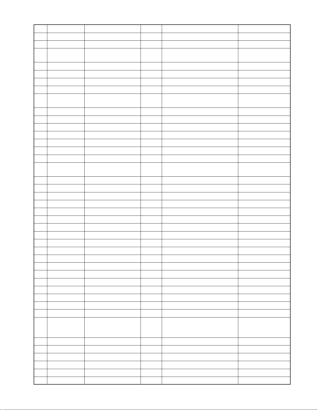
<< MICROCOMPUTER TERMINAL NAME AND OPERATION LOGIC >>
No. Terminal Name Function In/Out Logic Remarks
1 GND 0V
2 BA L INPUT BALANCE Out PWM out
3 REM OUT REMOTE CONTROL Out Remote control output
SIGNAL OUT
4 MUTE SOUND MUTE OUT Out Sound mute output
5 SP MUTE SPEAKER MUTE Out In muting = H
6 DEF POW Out
7 POWER POWER ON/OFF OUT Out Power control In ON=H
8 LED POWER LED OUTPUT Out Power LED on-control
LED lighting=L
9 POWER LNB Out 0V
10 LNB DET In 0V
11 SCL() IIC BUS CLOCK OUT Out IIC bus clock output 0
12 SDA() IIC BUS DATA IN/OUT In/Out IIC bus data input/output 0
13 SYNC VCD H SYNC INPUT In Main picture H. sync signal input
14
15 AFT2 IN In Sub tuner AFT S-curve input
16 AFT1 UV MAIN S-CURVE In Main tuner AFT S-curve
SIGNAL signal input
17 KEY A LOCAL KEY INPUT In Local key detection: 0 to 5V
18 KEY B LOCAL KEY INPUT In Local key detection: 0 to 5V
19 SGV TEST SIGNAL OUT Out Test signal output In normal=L 0V
20 SGA TEST AUDIO OUT Out Test audio output In normal=L 0V
21 VSS POWER GROUNDING — 0V: Gounding voltage 0V
22 R R Out At display on:Pulse
23 G G Out At dispaly on:Pulse
24 B B Out At dispaly on:Pulse
25 Y/BL BL Out At dispaly on:Pulse
26 HSYNC In HSYNC for OSD display Pulse
27 VSYNC In VSYNC for OSD display Pulse
28 OSC1 DISPLAY CLOCK Out 4.5MHz Pulse
29 OSC2 DISPLAY CLOCK In Pulse
30 TEST TEST MODE In GND fixed 0V
31 XIN SYSTEM CLOCK In System clock input 8MHz pulse
32 XOUT SYSTEM CLOCK Out System clock output 8MHz 8MHz pulse
33 RESET SYSTEM RESET In System reset input (In reset=L) 5V
34 SW IN
35 RMT IN REMOTE CONTROL IN In remote control pulse input=L In reception of
SIGNAL INPUT remote pulse
36 SYNC AV1 HSYNC INPUT In External H. sync signal input Pulse
37 SCL1 IIC BUS CLOCK OUT Out IIC bus clock output 1 Pulse
38 SDA1 IIC BUS DATA IN/OUT In/Out IIC bus data input/output 1 Pulse
39 GND 0V
40 NC
41 ACP NSYNC INPUT In AC pulse input
42 VDD POWER — 5V 5V
3-5
Page 41
5. EEPROM (QA02)
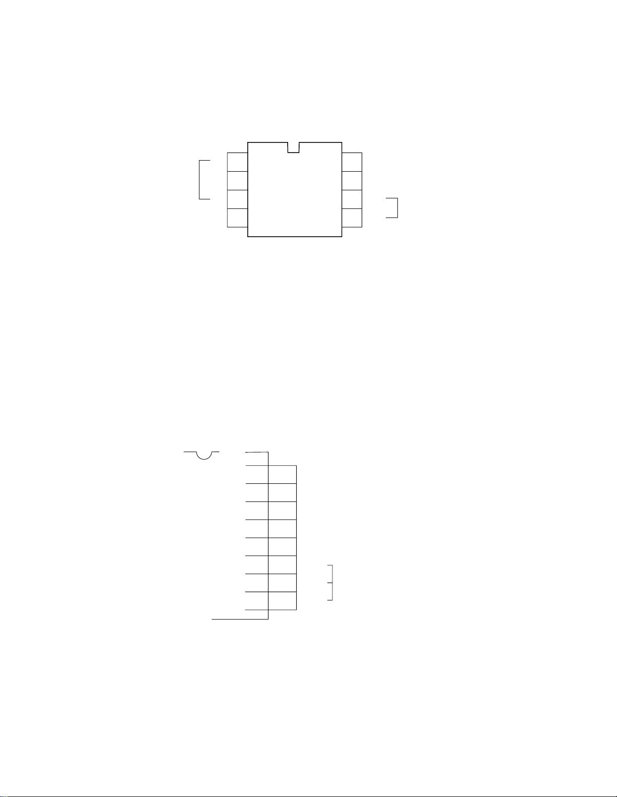
EEPROM (Non volatile memory) has function which, in spite of power-off, memorizes the such condition as channel selecting
data, last memory status, user control and digital processor data. The capacity of EEPROM is 8k bits. Type name is 24LC08BI/
P or ST24C08CB6, and those are the same in pin allocation and function, and are exchangeable each other. This IC controls
through I2C bus. The power supply is common to the EEPROM and the main MICOM. Pin function of EEPROM is shown in
Fig. 3-3.
EEPROM(QA02)
1
Device address
GND
A0
A1
A2
Vss
2
3
4
Fig. 3-3
8
7
6
5
Vcc + 5V
NC
SCL
SDA
2
I
C-BUS line
6. ON SCREEN FUNCTION
ON SCREEN FUNCTION indicates data like channel, volume. Formerly, exclusive use of OSD IC was used, but in N5SS,
the OSD function is within the main microcomputer. Pin function concerning on-screen data generation is shown in Fig. 3-
4. Oscillation clock of OSD is approx. 4.5MHz. 9MHz which becomes multiplied by two to become the dot clock i slocated
within the microcomputer. For oscillation, a coil TRF1160D (LA02) is used.
QA01
OSC2
OSC1
VD
HD
Y/BL
O
I
I
I
O
B
O
G
O
R
O
OSC2 OSC OUT
29
OSC1 OSC IN
28
VSYNC H. SYNC SIGNAL
27
HSYNC V. SYNC SIGNAL
26
Ys/Ym HALF TONE SIGNAL
25
BOUT
24
GOUT COLOR SIGNAL
23
ROUT
22
V
G
Fig. 3-4
3-6
Page 42
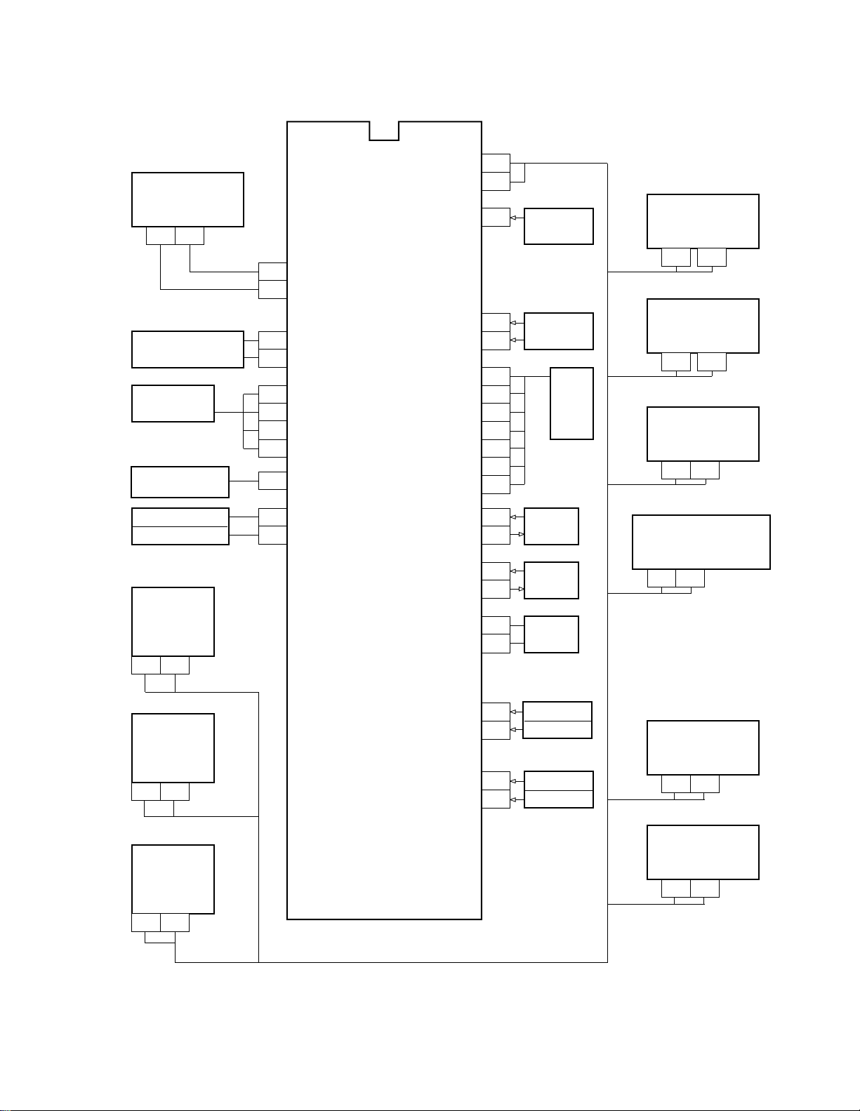
7. SYSTEM BLOCK DIAGRAM
QA01
TMP87CS38N-3152
MEMORY
24LC08B1/P
SDA SCL
5 6
H. SYNC PULSE
V. SYNC PULSE
VIDEO SIGNAL
PROCESS CIRCUIT
REMOTE CONTROL
OUTPUT
SOUND MUTE
SPEAKER MUTE
Q701
C/C, EDS
XC144144P
DATA CLK
QA02
11
12
26
27
22
23
24
25
3
4
5
SCL 0
SDA 0
HSYNC
VSYNC
R
G
B
YS/TM
RMT OUT
MUTE
SP MUTE
SDA 1
SCL 1
RMT
KEY-A
KEY-B
RST
VDD
GND
VSS
POWER
ACP
LED
XIN
XOUT
OSCI
OSCO
SGV
SGA
38
37
35
17
18
33
42
1
21
7
41
8
31
32
28
29
19
20
REMOTE
SENSOR
UNIT
KEY SWITCH
POWER
SUPPLY
CIRCUIT
8MHz
CLOCK
6.1MHz
CLOCK
SIGNAL
OUTPUT
H001
MAIN U/V TUNER
EL446L
SDA SCL
HY01
SUB U/V TUNER
EL922L
SDA SCL
Q501
VCD
TA1222N
SDA SCL
27 28
H002
IF/MPX
MVUS345
SDA SCL
21 20
DPC UNIT
DATA CLK
QY04
PIP CONTROL
DATA CLK
6 5
SYNC-AV1
AFT1 IN
SYCN-AV2
AFT2 IN
Fig. 3-5
3-7
36
16
13
2
MAIN SCREEN
SYNC DET.
AFT DET.
SUB SCREEN
SYNC DET.
AFT DET.
QV01
AV SW
TA1218N
SDA SCL
26 27
QM01
DSP
SDA SCL
Page 43
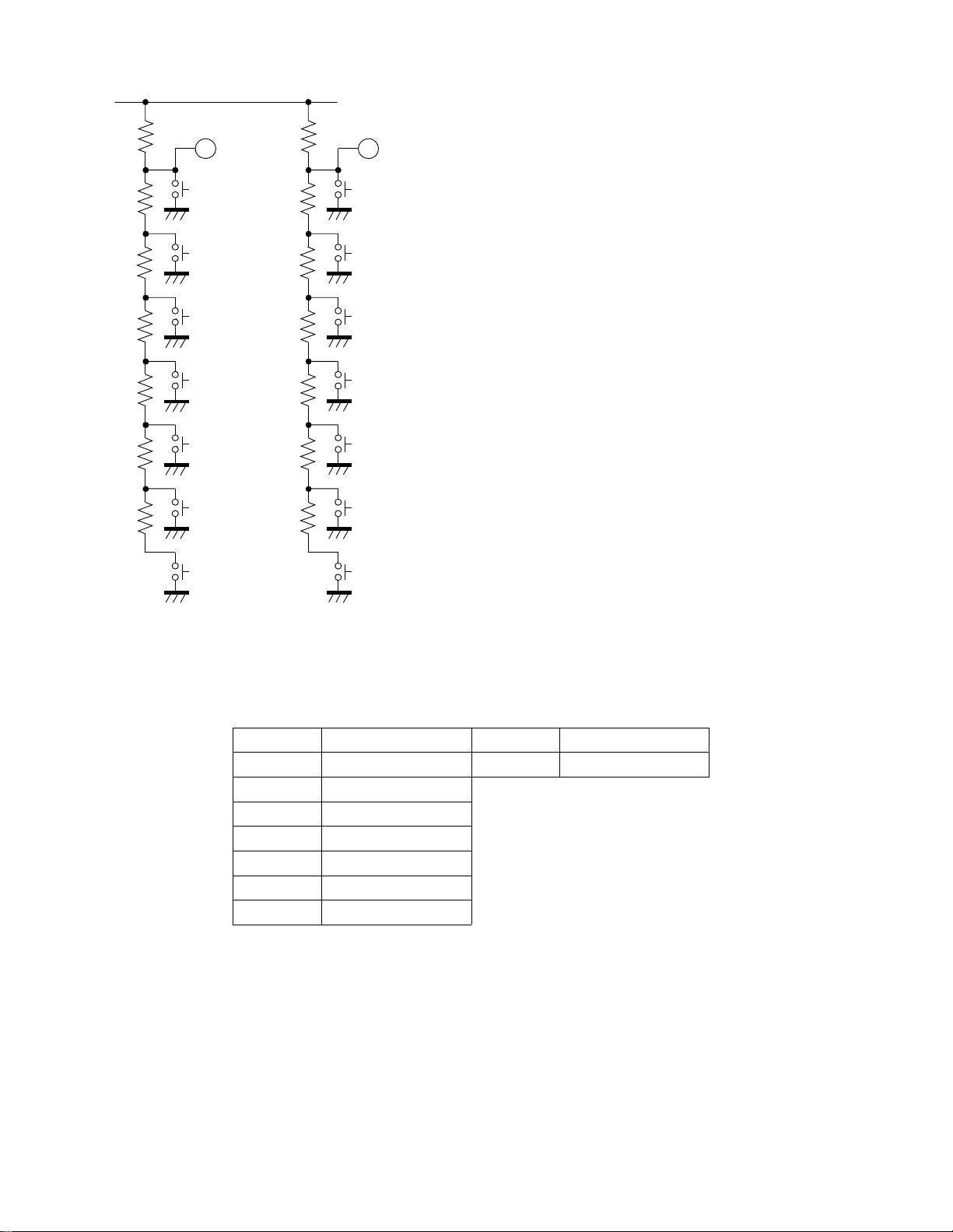
8. LOCAL KEY DETECTION METHOD
15
S15-1
S15-2
S15-3
16
S16-1
S16-2
S16-3
Local key detection in the N5SS chassis is carried out by
using an analog voltage divider-like method which detects
a voltage appearing at the local key input terminals (pins 17,
18) of the microcomputer whenever a key is depressed.
Using this method, a maximum of 14 keys can be interpreted.
The circuit diagram shown at the left is a representation of
the local key circuit. As can be seen from the diagram, when
one of keys among SA-01 to SA-08 is pressed, each of two
input terminals (pins 17, 18) develops a voltage (Vin)
corresponding to the key pressed. (The voltage measurement
and key identification are carried out by an A/D converter
inside the microcomputer along with interpreting software.
S15-4
S15-5
S15-6
S15-7
Fig. 3-6. Local key assignment
Key No. Function Key No. Function
SA-02 POWER SA-01
SA-03 CH UP
SA-04 CH DN
SA-05 VOL UP
SA-06 VOL DN
SA-07 ANT/VIDEO, ADV
SA-08 MENU
S16-4
S16-5
S16-6
S16-7
Table 3-1 Local key assinment
DEMO START/STOP
3-8
Page 44
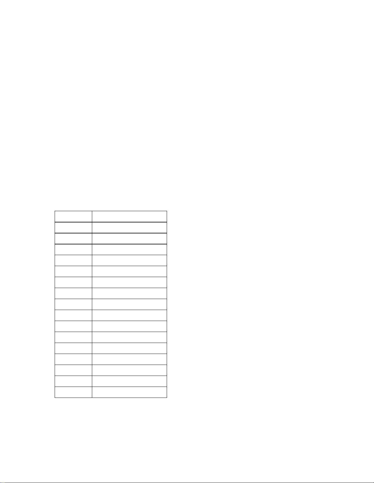
9. ENTERING THE SERVICE MODE
11. SERVICE ADJUSTMENT
1. PROCEDURE
(1) Press once MUTE key on the remote hand unit to
indicate MUTE on screen of the television.
(2) Press the MUTE key of remote hand unit again and
keep depressed while depressing the MENU key on
the front of the unit.
2. During service mode, indication S is displayed at upper
right corner on screen.
10. TEST SIGNAL SELECTION
1. In OFF state of test signal, SGA terminal (Pin 20) and
SGV terminal (Pin 21) are kept at a “L” condition.
2. The function of VIDEO test signal selection is cyclically
changed with each depression of the VIDEO key (on the
remote control unit).
Table 3-2
Test Signal No. Name of Pattern
1. ADJUSTMENT MENU INDICATION ON/OFF,
MENU key ( on TV set)
2. During display of the adjustment menu, the following
functions are possible:
a) Selection of adjustment item :
POS UP/DN key (on TV/remote unit)
b) Adjustment of each item :
VOL UP/ DN key (on TV / remote unit)
c) Direct selection of adjustment item
R CUTOFF : 1 POS (remote unit)
G CUTOFF : 2 POS (remote unit)
B CUTOFF : 3 POS (remote unit)
d) Data setting for PC unit adjustment
SUB CONTRAST : 4 POS (remote unit)
SUB COLOR : 5 POS (remote unit)
SUB TINT : 6 POS (remote unit)
e) Horizontal line ON/OFF : VIDEO (TV)
(NOTE: applies only to direct view)
f) Test signal selection : VIDEO (remote unit)
* In service mode, serviceable items are limited.
3. Test audio signal ON / OFF : 8 POS (remote unit)
* Test audio signal : 1kHz
0 Signal OFF
1 All black signal + R single color (OSD)
2 All black signal + G single color (OSD)
3 All black signal + B single color (OSD)
4 All black signal
5 All white signal
6 W/B
7 Black cross bar
8 White cross bar
9 Black cross hatch
10 White cross hatch
11 White cross dot
12 Black cross dot
13 H signal (bright area)
14 H signal (dark area)
15 Black cross + G
4. Self check display : 9 POS (remote unit)
* Cyclic display (including ON/OFF)
5. Initialization of memory :
CALL (remote unit) + POS UP (TV)
6. Initialization of self check data :
CALL (remote unit) + POS DN (TV)
7. BUS OFF :
CALL (remote unit) + VOL UP (TV)
(3) SGA (audio test signal) output should be square
wave of 1kHz.
3-9
Page 45
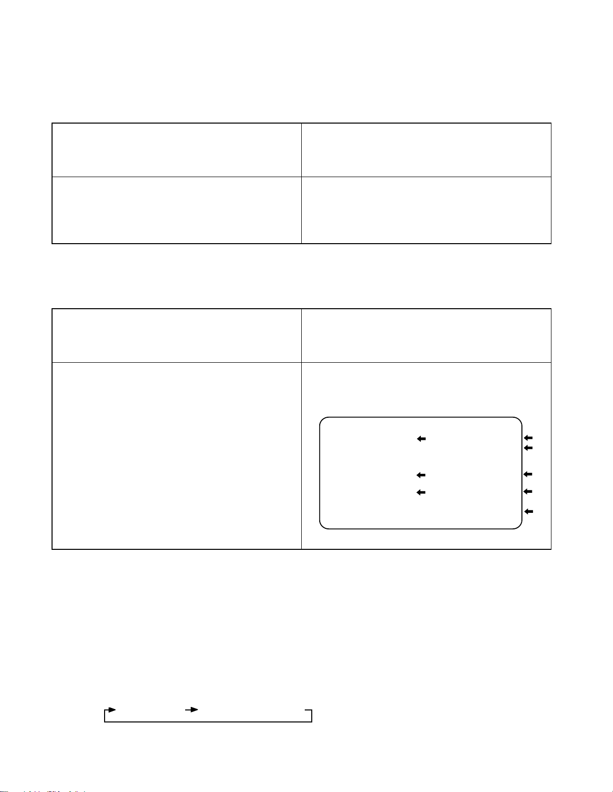
12. FAILURE DIAGNOSIS PROCEDURE
The N5SS chassis is equipped with a self diagnosis function inside, used for troubleshooting.
1. CONTENTS TO BE CONFIRMED BY CUSTOMER BEFORE SERVICE CALL IS MADE
Table 3-3
Contents of self diagnosis Display items and actual operation
A. DISPLAY OF FAILURE INFORMATION
Power indicator lamp blinks and picture does not come.
IN NO PICTURE (Condition of display)
1. When power protection circuit operates;
2. When I2C-BUS line is shorted;
1. Power indicator red lamp blinks. (0.5 seconds interval)
2. Power indicator red lamp blinks. (1 seconds interval)
If these indication appears, repairing work is required.
2. CONTENTS TO BE CONFIRMED BY SERVICER (Check in self diagnosis mode)
Table 3-4
Contents of self diagnosis Display items and actual operation
Contents of self diagnosis
Display items and actual operation
<Countermeasure in case that phenomenon always arises.>
B. Detection of shortage in BUS line
C. Check of comunication status in BUS line
D. Check of signal line by sync signal detection
E. Indication of part code of microcom.(QA01)
F. Number of operation of power protection circuit
NO. 239XXXX
POWER: 000000
BUS LINE: OK
BUS CONT: OK
BLOCK: UV V1 V2
QV01, QV01S
(Example of screen display)
SELF CHECK
Part coce of QA01
Number of operation of
power protection circuit
Short check of bus line
Communication check of
busline
E
F
B
C
D
3. EXECUTING SELF DIAGNOSIS FUNCTION [CAUTION]
(1) When executing block diagnosis, select first the desired input signal source (U/V BS VIDEO1,2,3) screen, and then enter
the self diagnosis mode.
(2) When diagnosing other input modes, repeat the diagnosis routines after source selection. The test signals and/or routines
apply only to the video source selected at the time of testing.
(PROCEDURE)
(1) Place the unit in the service mode.
(2) Press the “9” key on the remote control will display the self diagnosis results on screen.
With each key press the mode will change as shown below.
SERVICE mode SELF DIAGNOSIS mode
(3) To exit from the service mode, turn the power off via the front panel or remote control.
3-10
Page 46
4. UNDERSTANDING THE RESULTS OF THE SELF DIAGNOSIS FUNCTION
See Fig. 3-7 .
(Example of screen display)
SELF CHECK
NO. 239XXXX
POWER: 000000
BUS LINE: OK
BUS CONT: OK
BLOCK: UV V1 V2
QV01, QV01S
Part coce of QA01
Number of operation of
power protection circuit
Short check of bus line
Communication check of
busline
E
F
B
C
D
Fig. 3-7
Table. 3-5
Item Contents Instruction of results
BUS LINE Detection of bus line short Indication of OK for normal result, NG for abnormal
Indication of OK for normal result
Indication of failure place in abnormality
(Failure place to be indicated)
QA02 NG, H001 NG, Q501 NG, H002 NG
QV01 NG, Q302 NG, QY02 NG, HY01 NG
QD04 NG, QM01 NG, Q701 NG
BUS CONT Communication state of bus line Note 1. The indication of failure place is only one
placet though failure places are plural. When
repair of a failure place finishes, the next
failure place is indicated. (The order of
priority of indication is left side.)
BLOCK: UV1
UV2
V1
V2
The sync signal part in each video signal
supplied from each block is detected.
Then by checking the existence or non of
sync part, the result of self diagnosis is
*Indication by color
• Normal block :Green
• Non diagnosis block :Cyan
displayed on screen. Besides, when “9” key
on remote unit is pressed, diagnosis
operation is first executed once.
3-11
Page 47

<Clearing the self diagnosis results>
While the error count state is displayed upon the screen, press the “CHANNEL DOWN” button on TV set
pressing “DISPLAY” button on remote unit.
[CAUTION]
All ways observe the following caution, when in the
service mode screen.
• Do not press the “CHANNEL UP” button. This will cause
initialization of the memory IC. (Replacement of memory
IC is required.
• Do not initialize self diagnosis result. This will change user
adjusting contents to factory setting value. ( Adjustment is
required.)
White
Yellow
Cyan
Green
Magenta
Red
Blue
( COLOR BAR SIGNAL)
Color elements are positioned in sequence of high brightness.
<Troubleshooting method utilizing internal test signal> (VIDEO INPUT 1 terminal should be open.)
(1) With service mode screen, press VIDEO button on remote unit. If inner video signal can be received, QV01 and after are
normal.
(2) With service mode screen, press “8” button on remote unit. If sound of 1kHz can be heard, QV01 and after are normal.
* By utilizing signal of VIDEO input terminal, each circuit can be checked. (Composite video signal, audio signal)
3-12
Page 48
13. TROUBLE SHOOTING CHARTS
(1) TV DOES NOT TURNED ON
TV does not turned on.
Relay sound
YES
NO
Check of voltage at pin 7 of QA01
(DC 5V).
OK
8MHz oscillation waveform
at pin 32 of QA01.
OK
Pulse output at pins 37 and 38 of QA01.
OK
NG
NG
Check power circuit.
Check OSC circuit.
Replace QA01.
NG
Voltage check at pin 32 of QA01
(DC 5V)
NG
OK
Check reset circuit.
Check relay driving circuit.
Replace QA01.
3-13
Page 49
(2) NO ACCEPTION OF KEY-IN
Key on TV
Voltage change at pins 17, 18 of
QA01 (5V to 0V).
OK
Replace QA01.
Remote unit key
Pulse input at pin 35 of QA01,
When remote unit key is pressed.
OK
Replace QA01
(3) NO PICTURE (SNOW NOISE)
NG
Check key-in circuit.
NG
Check tuner power circuit.
No picture
Voltage at pins of +5V, and 32V.
OK
Check H001. Check tuner power circuit.
NG
3-14
Page 50
(4) MEMORY CIRCUIT CHECK
Memory circuit check
Voltage check at pin 8 of QA02 (5V).
NG
Pulse input at pins 5 and 6 of QA02
in memorizing operation.
Replace QA02.
Adjust items of TV set adjustment.
(5) NO INDICATION ON SCREEN
No indication on screen.
OK
NG
OK
Note: Use replacement parts for QA02.
Check power circuit.
Check QA01.
Check of character signal at pin 23
Input of OSC waveform at pin 29 of QA01
Check of sync signal at pins 26, 27 of QA01.
Replace QA01.
of QA01. (5V
with indication key pressed.
)
P-P
OK
OK
OK
3-15
NG
Check V/C/D circuit.
NG
Check OSC circuit.
Check sync circuit.
Page 51

NOTES
3-16
Page 52

SECTION IV
AUDIO OUTPUT CIRCUIT
4-1
Page 53
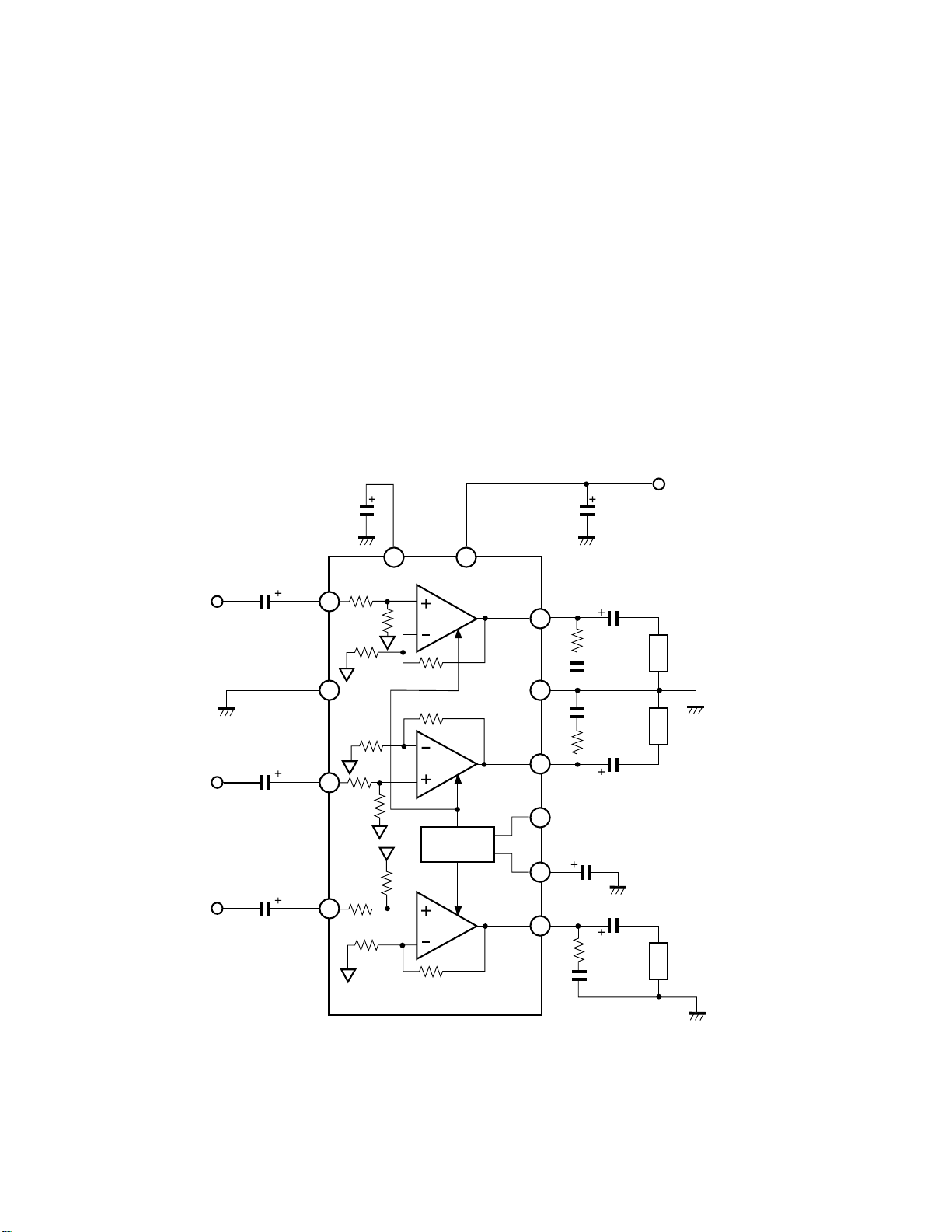
1. OUTLINE
The main amplifiers and woofer output amplifiers use a
bipolar IC (TA8256H) and develop output powers of
10Wx2 + 13W.
2. THEORY OF OPERATION
2-1. Operation of TA8256H
The TA8256H is a modified version of the TA8128AH
which was used in the N4SS chassis as an audio ouput IC.
In the TA8256H, one channel has been added and up to 3
channels can be used. Performance for each channel is the
same as that of the TA8218H. Fig. 4-1 shows a block
diagram of the IC.
47mF
Vcc
25.5V
47mF
6
4
L
3
2
1
W
RIPPLE FILTER
4k
30k
350
W
PRE
GND
350
W
4k
30k
30k
4k
350
W
F
1m
L
F
1m
R
1m
W
R
F
AMP-2
AMP-3
MUTING
AMP-1
20k
W
9
Vcc
OUTPUT-2
OUTPUT-3
OUTPUT-3
POW
GND
(R)
(S) or (W)
10
12
11
8
5
7
(mute)
2.2
W
0.12mF
0.12mF
2.2
W
(mute Tc)
2.2
W
0.12mF
470mF
470mF
1000mF
(L)
R
L
RL (R)
RL (W)
Fig. 4-1
4-2
Page 54

SECTION V
DSP CIRCUIT
5-1
Page 55
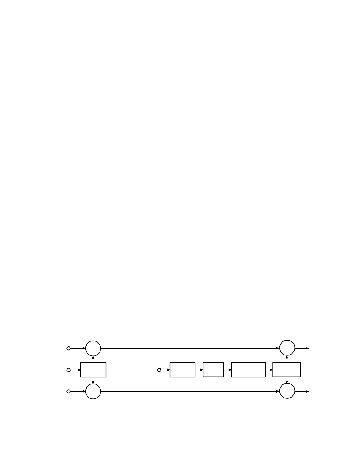
1. ORIGINS OF DOLBY SURROUND
Dolby Stereo movies and Dolby Surround video and television
programs include an additional sonic dimension over
conventional stereo productions. They are made using a Dolby
MP (Motion Picture) Matrix encoder, which combines four
channels of audio into a standard two-channel format, suitable
for recording or transmitting the same as regular stereo programs.
To recapture the dimensional properties brought by the
additional channels, a Dolby Surround decoder is used. In the
theatre, a professional decoder is part of the Dolby Stereo
cinema processor used to play 35 mm stereo optical prints.
The decoder recovers the left, center, and right signals for
playback over three front speakers, and extracts the surround
signal for distribution over an array of speakers wrapped
around the sides and back of the theater. (These same
speakers may also be driven from four of the six discrete
tracks on 70 mm Dolby Stereo magnetic prints, but in this
case no decoder is needed.)
Home viewing of movies on video has become extremely
popular, and with the advent of stereo VCR's, stereo television
and digital video discs, the audio side of the video presentation
has improved considerably, inviting the use of full-range
sound reproduction. The ability to deliver high quality audio
in these formats made it easy to bring MP Matrix-encoded
soundtracks into the home as well, thus establishing the
foundation for Dolby Surround.
2. THE DOLBY MP MATRIX
One of the original goals of the MP Matrix was to enable
Dolby Stereo soundtracks to be successfully played in theaters
equiped for mono or two-channel stereo sound. This allows
movies to be distributed in a single optical format, and
furtheremore results in complete compativility with home
video media without requiring separate soundtrack mixes.
Since the three front channels of the MP Matrix are assembled
in virtually the same way as a conventional stereo mix --- left
into left, center equally into left and right, and right into rightplaying a Dolby Stereo soundtrack over two speakers
reproduces the entire encoded soundtrack. There is but one
exception: the surround signal, though audible, is not
reproduced in its proper spatial perspective. When the first
home decoder was developed in 1982, its goal was to restore
this lone missing dimension.
Before we discuss decoders, it is necessary to see how the MP
Matrix encoder works. Referring to the conceptual diagram
in Fig. 5-1, the encoder accepts four separate input signals;
left, center, right, and surround (L, C, R, S), and creates two
final outputs, left-total and right-total (Lt and Rt).
The L and R inputs go straight to the Lt and Rt outputs without
modification, and the C input is divided equally to Lt and Rt
with a 3 dB level reduction (to maintain constant acoustic
power). The S input is also divided equally between Lt and Rt,
but it first undergoes three additional processing steps:
a. Frequency bandlimiting from 100 Hz to 7 kHz.
b. Encoding with a modified from of Dolby B-type noise
reduction.
c. Plus and minus 90-degree phase shifting is applied to
create a 180-degree phase differential between the
components feeding Lt and Rt.
It is clear there is no loss of separation between the left and right
signals; they remain completely independent. Not so obvious
is that there is also no theoretical loss of separation between the
center and surround signals. Since the surround signal is
recovered by taking the difference between Lt and Rt, the
identical center channel components in Lt and Rt will exactly
cancel each other in the surround output. Likewise, since the
center channel is derived from the sum of Lt and Rt, the equal
and opposite surround channel components will cancel each
other in the center output.
The ability for this cancellation technique to maintain high
separation between center and surround signals requires the
amplitude and phase characteristics of the two transmission
channels to be as close as possible. For instance, if the center
Left
Center
Right
+
+
-3dB
+
+
Surround
-3dB B.P.F
Fig. 5-1 Conceptual Dolby Stereo/Dolby Surround encoder
5-2
DOLBY NR
ENCORDER
+
+
+90 DEG
-90 DEG
+
+
Lt
Rt
Page 56
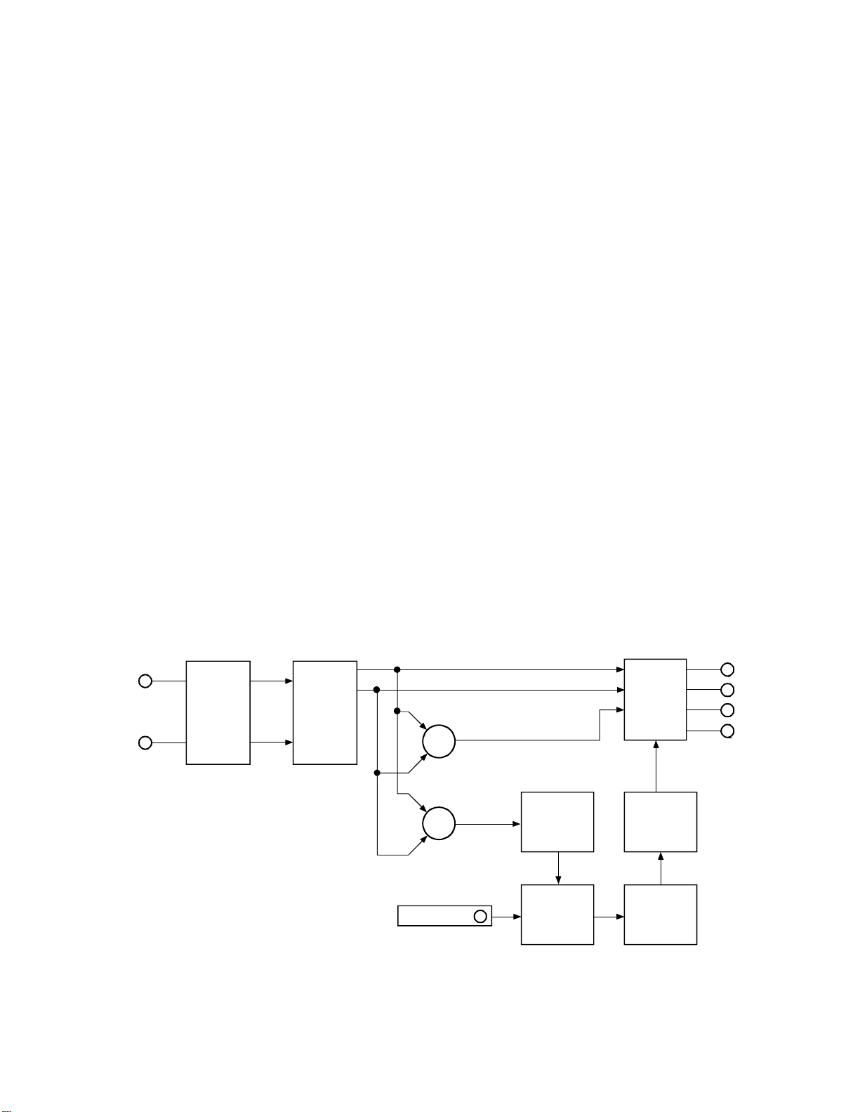
channel components in Lt are not identical to the ones in Rt
as a result of a channel balance error, center information will
come out of the surround channel in the form of unwanted
crosstalk.
3. THE DOLBY SURROUND DECODER
This leads us to the original Dolby Surround decoder. The
block diagram in Fig. 5-2 shows how the decoder works.
Except for level and channel balance corrections, the Lt input
signal passes unmodified and becomes the left output. The Rt
input signal likewise becomes the right output. Lt and Rt also
carry the center signal, so it will be heard as a "phantom"
image between the left and right speakers, and sounds mixed
anywhere across the stereo soundstage will be presented in
their proper perspective. The center speaker is thus shown as
optional since it is not needed to reproduce the center signal.
The L-R stage in the decoder will detect the surround signal
by taking the difference of Lt and Rt, then passing it through
a 7 kHz low-pass filter, a delay line, and complementary
Dolby noise reduction. The surround signal will also be
reproduced by the left and right speakers, but it will be heard
out-of-phase which will diffuse the image.
Since the heart of the decoding process is a simple L-R
difference amplifier, it is referred to generically as a "passive"
decoder. This is to distinguish it from decoders using active
processes to enhance separation which are known as "active"
decoders.
4. DSP CIRCUIT
A surround component (L-R) is extracted from L, R audio
signals coming through the AV SW in the matrix circuit as
shown in Fig. 5-3. The surround component enters the DSP
circuit through the LPF.
The signal is A/D converted, delayed by an arbitrary time of
0~100 msec (every 3.2 msec) by digital process and then D/
A converted and outputs from the DSP IC. The DSP IC
develops two outputs; (LO) for FRONT (LO) and (RO) for
REAR and each output is controlled by the microcomputer
for each surround mode. The output signal (LO) for FRONT
is added and subtracted with the input signal in a matrix
circuit and output from the front speaker in passing through
the audio processor and main amplifiers.
At the same time, the output signal (RO) for REAR is fed to
the Dolby NR circuit, but switched to "Dolby surround"
mode, and then output from the rear speaker in passing
through audio processors and rear main amplifiers.
In this case, the DSP stands for not only a simple digital
surround processor but also a digital surround field processor.
That is, it works to give a simple surround effect but to give
effect as if the listener can feel reality suitable for the
programs. For example, it aims to give the listeners a reality
matching to each program they are enjoying in their home
listening room so that they can obtain reality of big concert
hall or feel as if they are watching a move at a reserved seat
in a movie theater.
INPUTS OUTPUTS
L L
Lt
INPUT
BALANCE
CONTROL
Rt
LEVEL
CONTROL
DELAY SET
R R
C
L+R
Optional passive center si
S
L-R
FILTER
ANTIALIAS
AUDIO
DELAY
gnal
C
MASTER
LEVEL
CONTROL
S
MODIFIED
B-TYPE NR
DECODER
7 kHz
LOW PASS
FILTER
Fig. 5-2 Passive surround decoder block diagram
5-3
Left
ght
Ri
Center
Surround
Page 57
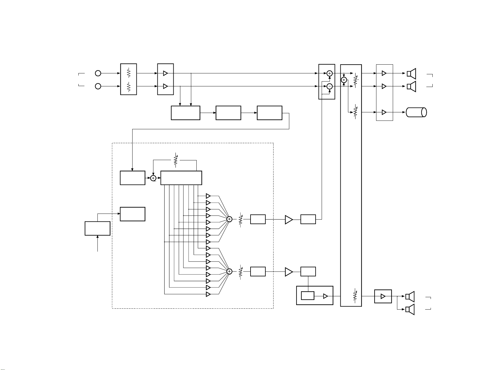
From
A/V SW
L
IN
R
Fig. 5-3 Block diagram of DSP circuit
5-4
QD08
Input Balance
4
A/D
QD01
Input Buffer
12 14
10 8
(L-R CIRCUIT)
VC
DIGITAL DELAY
R L
6 5
MATRIX
7 3
(L-R)
QD01
QD03 DSP IC YM7128 B
TO
LPF
1 3 1
LPF
QD01 QD02
QD02
DSP
Front Addition Circuit
5
L
R
10
7
8
9
Front amp
L
R
L+R
Audio
Processor
(H002)
Q670
L+S
R-S
L
Speaker
R
Sycrone
(Super woofer)
QD04
BUS
CONVERT
From Micro
computer
CONT
VL
VR
D/A
D/A
Buffer
LO
3 1 5 7
LPF
7
QD05 QD05
Buffer DQ06
RO
5 7 3
8
QD06
LPF
1
6
QD07 DQ02
LO
Dolby NR
9 14
12
Rear Amp
L-R
Q640
+S
L
Speaker
R
Page 58
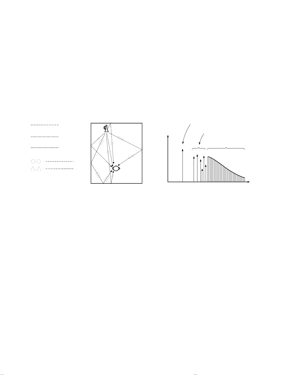
As shown in Fig. 5-4, a sound emitted in a sound field can
S
be classified as a direct sound which directly reaches ears of
a listener, and reflected sound which comes after collision
with a wall as shown by dotted line or comes after several
times of collision as shown by double dotted lines. The
listeners are determining that they are listing in what type of
location by perceiving time difference and volume level
difference between the direct sound and the reflected sound.
For more detail, this situation can be expressed with the
direct sound, initial reflection sound coming after one time of
reflection, and trains of reverberation sound in later period as
shown in Fig. 5-5.
The DSP circuit develops these initial reflection sound and
the reverberation sound artificially and add them to the
original sounds, thereby creating rhe effect that allows the
listeners in the home listening room to feel as if they are
listening in an original location.
The DSP IC YM7128B has eight separate output taps and
their delay time and the output levels can be specified
separately, so, various sound fields can be selected by varying
the initial reflection sound. Moreover, the IC has an internal
feedback loop which controls the delay time and the output
level in considering the later time reverberation sound.
Direct Sound
ound Level
Initial Reflection
Sound
Reverberation
Sound
:
:
Direct Sound
Initial Reflection Sound
Reverberation Sound
Time
Fig. 5-4 Fig. 5-5
5-5
Page 59
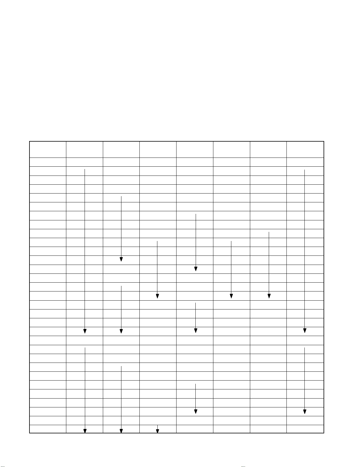
5. DSP (Digital Surround Processor) IC
Input signal entered into analog input pin 4 of DSP IC QD03
(YM7128B) is converted to 14 bit digital signal with the
sampling frequency 23.6 kHz by A/D converter of 14 bit
floating system, and enters digital delay circuit through
digital attenuator VM and doubler.
The digital delay circuit has nine output taps, and the delay
time of each tap can be controlled independently, also each
tap position can be switched by T0 to T8 register.
In a minute, the T0 output passes through the primary FIR
(Finite Impulse Response) type low pass filter, and reduction
processing is performed by VC, then it feed-backed to the
Table 5-1 DSP control factor
Mode OFF DOLBY THEATER STADIUM NIGHT CLUB CONCERT UNIT
Control SURROUND HALL HALL
-VM (IN) -•¥ P-0 P0 ¥ P0 P0 P0 dB
VL (LO) -•¥ P0~ -• P0~ -¥• P0~ --¥ • P0~ --¥•
VR (RO) P0 P0 P0 P0 P0
VC (Echo) -•¥ -•¥ M-6 M-10 M-8
GL1 P-4 M-2 M-2 P-2
2 M-6 -•¥ P-4 P-10
3 P-12 P-6 P-16
4 P-12 M-10 -•¥
5-•¥-•¥
6
7
8
GR1 P0
2-•¥P0
3 P-18
4-•¥
5 P-2 P-6 P-4
6 M-2 M-6 P-8
7 P-8 M-10 P-8
8 P-10 P-12 P-14
T0 (Delay) 0 0 0 100.0 19.4 51.6 msec
1 19.4 12.9 93.6 12.9 71.0
2 0 38.7 100.0 19.4 83.9
3 71.0 100.0 22.6 100.0
4 87.1 0 29.0 0
5 29.0 6.5 64.5
6 45.2 9.7 80.7
7 83.9 25.3 90.4
8 100.0 35.5 100.0
C0 (Filter) 0 0.71875 0.59375 0.875 —
1 0.28125 0.40625 0.125 —
delay input after it is added to the doubler described above.
The output of eight taps T1 to T8 is added after performing
reduction processing by GL1~GL8, GR1~GR8, and reduction
processing is performed by the digital attenuator VL or VR,
and an analog output is created by D/A converter after
passing through digital filter, comes out from pin 7 or 8.
The digital attenuated value, delay time and the coefficient of
FIR type low pass filter are set by writing the data on the
register.
This process is performed by loading three data from sub
microcomputer to microcomputer interface.
This unit has four modes as surround mode. The setting
values are described in Table 5-1.
5-6
Page 60
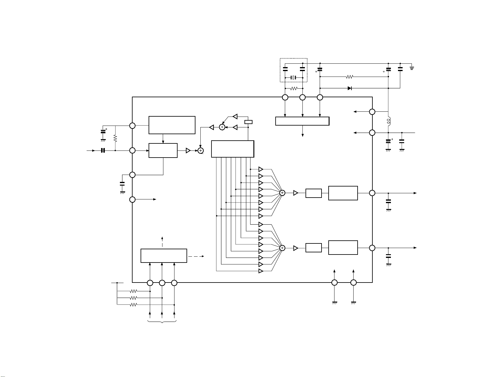
XD01
5-7
Fig. 5-6
From
Input LPF
CD22
CD15
CD23
VDD
RD26
QD03
CV
5
REFERENCE
VOLTAGE
GENERATION
AIN
4
CH
3
/TI
6
A/D
CONVERTER
MICROCOMPUTER
INTERFACE
DIN AO SCI
14 13
15
VM
C1
VC
C2
DIGITAL DELAY
T8 T7 T6 T5 T4 T3 T2 T1
TO
CD27 RD32 CD29
CD28
D01
RD33
11
12
16
XO XI /IC
D
TIMING GENERATION
Vss
AV
DD
1
LD01
2
+B (5V)
CD21 CD20
GL1
GL2
GL3
GL4
GL5
GL6
GL7
GL8
GL1
GL2
GL3
GL4
GL5
GL6
GL7
GL8
VL
VR
2fs
2fs
CONVERTER
CONVERTER
V
SS
10
D/A
D/A
LO
7
DC26
RO
8
To LPF Output
(For FRONT ch)
To LPF Output
(For REAR ch)
DC25
AV
SS
9
From Bus convert
(ICD04)
Page 61

NOTES
5-8
Page 62

SECTION VI
A/V SWITCHING CIRCUIT
6-1
Page 63

1. OUTLINE
The A/V switching circuit selects the desired video and
audio signals from the various inputs. It is controlled by the
microcomputer through IIC bus.
2. IN/OUT TERMINALS
TUNER INPUT U/V Tuner (Main)
U/V Tuner (PIP)
EXTERNAL INPUT VIDEO 1 With S-terminal
VIDEO 2
VIDEO 3 (Front) With S-terminal
OUTPUT VIDEO OUTPUT (V, L, R)
AUDIO ON SUB-PICTURE
3. CIRCUIT OPERATION
This circuit consists of A/V SW IC; TA1218N (QV01), and
selects signals from U/V tuner (Main), U/V tuner (PIP),
E1, E2 and E3.
3-1. Composite Video Signal
The selected video signal is output to pin 38 of QV01, and
separated by comb filter into Y an C. The resulted signal
is input to pins 30 and 32 of QV01, and is output to pins 36
and 34 to be supplied to Q501 (V/C/D).
Video signal for PIP is output to pin 42 of QV01, and is
supplied to PIP unit (ZY01).
3-2. S-Video Signal
When a cable is connected to S-VIDEO terminal, inner
switch of S-VIDEO terminal is shorted to ground to turn off
the transistor (QV05 for VIDEO1 input) for S-VIDEO
terminal detection. Then chroma input terminal (Pin 14 for
VIDEO1 input) of QV01 turns on.
6-2
Page 64
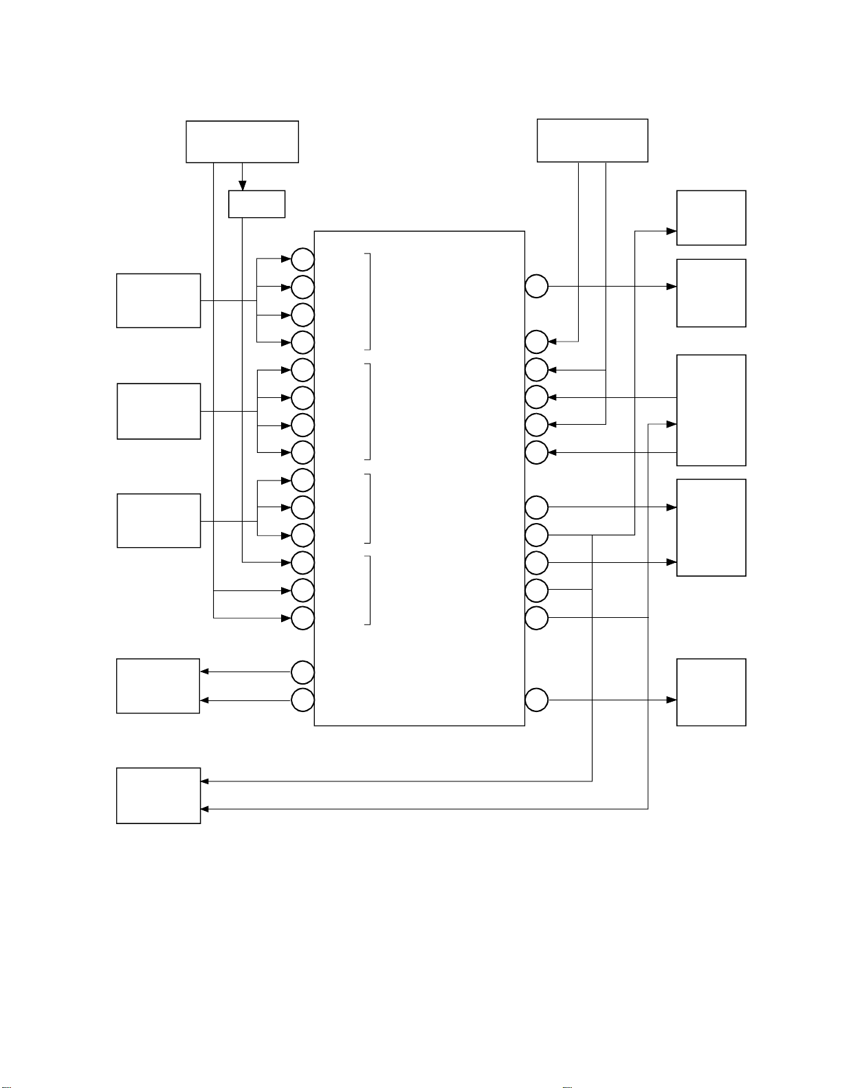
AV SW CIRCUIT
VIDEO 3
VIDEO 1
VIDEO 2
H002
IF/MTS/A. PRO
A
V
EQ
18
17
16
15
14
13
12
11
10
HY01
PIP TUNER/IF
V
QV01 T A1218N
C in
Y in
C in
C out
R out
26
28
29
30
31
32
34
35
R in
S in
L in
C in
R in
S in
L in
V in
R in
9
L in
8
SYNC OUT
PIP TV in
PIP L in
PIP R in
A
DSP
L/R in
QA01
SYNC in
COMB
FILTER
Y out
V in
C out
C in
Q501
PIP AUDIO
OUT JACK
TP48E90 ONLY
A/V OUT
JACK
7
6
5
2
1
V in
R in
L in
PIP R out
PIP L out
Fig. 6-1
Y out
L out
V out
PIP V out
42
36
37
38
Y in
PIP
V in
6-3
Page 65

NOTES
6-4
Page 66

SECTION VII
VIDEO PROCESSING CIRCUIT
7-1
Page 67
1. OUTLINE
This circuit converts and amplifies video signal (Luminance
and chroma signals) separated into Y/C, to original color
signal, and is supplied to CRT Drive circuit.
2. SIGNAL FLOW
by RGB matrix. Next the signal is superimposed with
OSD signal to be output to pins 41, 42 and 43, and is
supplied to CRT Drive circuit.
(4) The signal for Scan Modulation is processed with
differential in Q501 to be output to pin 48 Besides, at
terminal for adjustment TP501, luminance and chroma
signals are automatically output according to the
selected items of service mode.
Signal flow chart is shown in figure 6-1 Block diagram.
(1) Luminance signal is input to pin 15 of Q501, and enters
into delayline inside Q501 to be output to pin 4.
(2) Chroma signal is input to pin 13, and I/Q signal which
is demodulated in color, is output to pins 5 and 6, and
next supplied to pins 51 and 52.
(3) The signal is processed on luminance and chroma
signals, and is converted to original color signal (R,G,B)
Table 7-1
Pin No. Name Description
Pin 1 CW output 3.58MHz synchronized with burst is output. This is used for clock of comb filter.
Pin 10 Xtal 1 Terminal for 3.58MHz OSC crystal
Pin 11 APC filter Terminal for phase detection of color sync (OSC frequency control)
Pin 18 SYNC Sync-separated sync signal is output. It is used for detecting no signal in
microcomputer.
3. CIRCUIT OPERATION
All processing operation of video signal are done inside
Q501. The outline of Q501 (TA1222N) is explained in the
next section. Here, major terminals excepting input/output
terminals of Q501 are described.
Pin 30 HD Terminal for output of HD pulse syncronized with horizontal sync., and for input
of black expading mask pulse. It is used for timing pulse of OSD, C.C (Closed
Caption) in micro- computer.
Pin 32 Ys OSD change-over pulse input: Ys of OSD is input.
Pin 45 ABL Terminal for ABL control input
Pin 47 Ym Input of pulse for half tone control: It is supplied from microcomputer.
Pin 49 APL DET Detecting average level of video signal for correction of DC transmission
Pin 50 BLACK DET Detecting black area of video signal for black expading circuit
Pin 54 COL Terminal for peak-hold of color limiter
Pin 55 DAC1 Test point (TP501): Functioning test point in service mode
7-2
Page 68
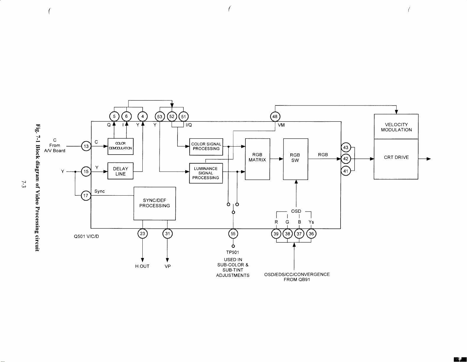
Page 69

NOTES
7-4
Page 70

SECTION VIII
V/C/D/IC
8-1
Page 71
1. OUTLINE
This IC enables more precise picture setting than that of former IC (TA8845N) by means of large scale employment
of IIC bus, and reduces many peripheral components by containing filters inside.
The main features (comparing TA8845) are as follows.
2. LARGE SCALE EMPLOYMENT OF BUS CONTROL OF PARAMETER FOR PICTURE CONTROLS
Soft method of picture making
Table 8-1
Former/TA8845N TA1222N
* Black expanding start point External constant BUS control
* DC transmission correction quantity point External constant BUS control
* Black level correction quantity External constant BUS control
* Each ABCL characteristic External constant BUS control
3. EMPLOYMENT OF CONTAINING EACH VIDEO BAND FILTER INSIDE
Employment of automatic adjustment circuit by Fsc to absorb deviation / Employment of deviation aborbing method by high
S/N filter and mask triming using fixed CR
Table 8-2
Former/TA8845N TA1222N
* Y-DL Apa-con DL inside Inside
* Chroma TO/BPF External Inside
* Velocity modulation processing circuit External Inside
* Fsc trap for chroma demodulation output External Inside
4. EMPLOYMENT OF CONTAINING EACH FILTER (FOR S/H) INSIDE
Circuit operation by extremely low current / Employment of leak current cancel circuit Employment of detection circuit
which does not suffer from influence of stray capacity
Table 8-3
Former/TA8845N TA1222N
* Chroma ACC / killer filter External Inside
* Y / color difference clamp filter External Inside
* Filter for filter automatic adjustment External Inside
* AFC 2 filter External Inside
8-2
Page 72

5. LOW COST OF IC
* Involving peripheral components inside ——> Down sizing of chip ——> Newly employment (NPN Tr area ratio to former
: -25%) of miniature process (PLAS-1 S process)
* Involving peripheral components inside——>Increasing of power consumption——>2 power supply system (5V / 9V
used)
* Involving peripheral components inside ——> Reducing of number of elements ——> Employment of new circuit
(1) Reducing of gate (change of preset method) of register for IIC decoder
(2) Reducing of DAC elements (employment of rudder type DAC + temperature compensation circuit)
(3) Deletion of chroma CW, ACC (employment of 90 degree shift phase circuit with automatic adjustment)
8-3
Page 73
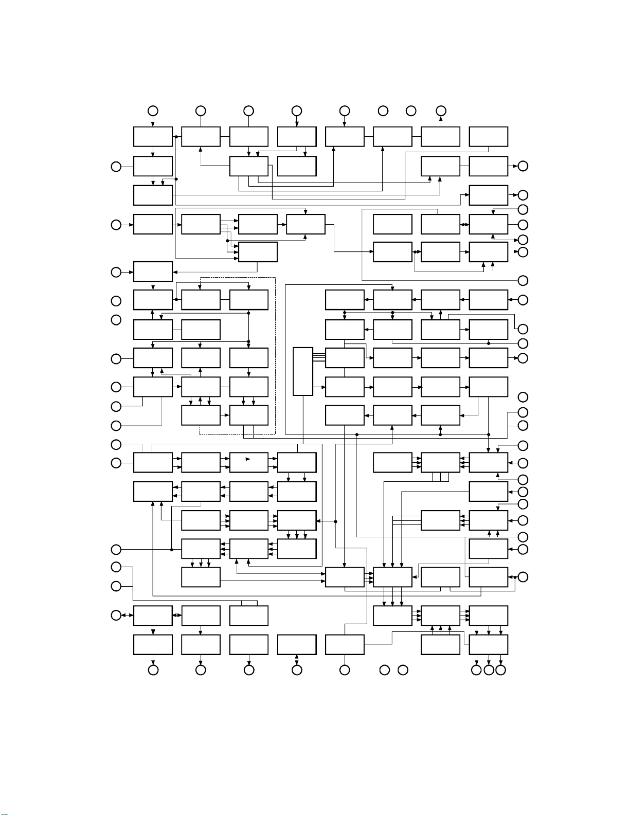
8-4
VCD BLOCK DIAGRAM (TA1222N)
HD OUT/BLACK
EXPAND MATRIX
SCP OUT
(SAND CASTLE)
1H DL CONTROL
(FOR PAL)
CW OUT/
COLOR IDENT.
V. Sep
Y IN 15
CHROMA IN
GND
APC FILTER
X tal-1
(3.58MHz)
X tal-2 (PAL)
X tal-3 (PAL)
16
13
34
129V
11
10
9
8
GND
VCC
(88)
SYNC IN
17
H. V.
SYNC SEP
V. SEP
V.
SYNC SEP
SYNC CHIP
CLAMP
SW
ACC AMP
ACC DET
APC DET
CHROMA
VCO
AFC1
20
PHASE DET
<APC-1>
DELAY
LINE
TOF
SUB
COLOR
P/N IDENT
BET
CW
MATRIX
FILTER
AUTO ADJ
3'5" VCD
21
32 FM VCO
H.
COUNT DOWNH.PARABOLA
FDC TRAP
BPF
SW
CHROMA
BLK
CHROMA
DEMOD.
LPH
FSC TRAP
BLK/AFC IN
25
H. BLK
S
R
T
SW
BENDING
CORRECTION
24
PHASE DET
<APC-2>
GAMMA
CORRECTION
B.C
RESTORE
SHARPNESS
DELAY LINE
SHARPNESS
CONTROL
WPS HALF TONE
19
GND (DEF) VCC (DEF)
H. PHASE
CONVERTER
DELAY LINE
LEVEL COR.
A.P.L DET
T. NR AMP SUB CONT
SHIFT
D/A
BLACK
HPF
Daf vCC
22 23
H. out
H. DRIVE
Y.
COUNT DOWN
REGISTER
DELAY LINE
BLACK
STRETON
BLACK
PEAK DET
TM AMP VM MUTE
CLAMP
H. DUTY
SW
Y.P OUT
SYNC
OUT
I2C BUS
DECODER
S W
TOK
Y. CLAMP
WHITE
PEAK DET
UNI COLOR
VCC
(98)
31
VER OUT
18
SYNC OUT
27
SDA
26
GND
19
SCL
4
Y1 OUT
29 GND
53 Y2 OUT
BLACK PEAK
30
HOLD
APL DET
39
VM OUT
28
26
Q OUT
5
6 Y OUT
I IN
Q IN
COLOR LIMITER
DAC 2
DAC 2
SECAM CONTROL
(FOR SECAM)
51
52
54
55
56
3
IQ/UV
CLAMP
UNI COLOR
SECAM
CONTROL
CW OUT
1
FRESH
COLOR
COLOR
AXIS
G-Y MATRIX
COLOR
PEAK DET
HI BRIGHT
COLOR
COLOR
SYS IDENT
1H DL
CONTROL
7
IQ UV
CONVERT
TINF
CLAMP
CDE
DAC 1/2
S.C.P
OUT
2
SW
DELAY
TIME
HALF
TONE
COLOR
GAMMA
HD OUT
EXT EFP IN
30
RGB
MATRIX
POWER OFF IN
YM SW
47
IN
M
Y
RGB
BRIGHT
SW
DRIVE CLAMP
VCC (98) GND
46 44
CLAMP
CLAMP OSD AMP
PEAK
ACL DET
CONTRAST
YS SW
YS SW
ABCL AMP
BLK
RGB OUTCUT OFF
41 42 43
B OUT
G OUT
33 B IN
34 G IN
35 R IN
36 OSD Ys IN
37 OSD B IN
38 OSD G IN
39
22 Ys IN
25 ABL IN
R OUT
OSD R IN
Page 74

SECTION IX
PIP MODULE
9-1
Page 75
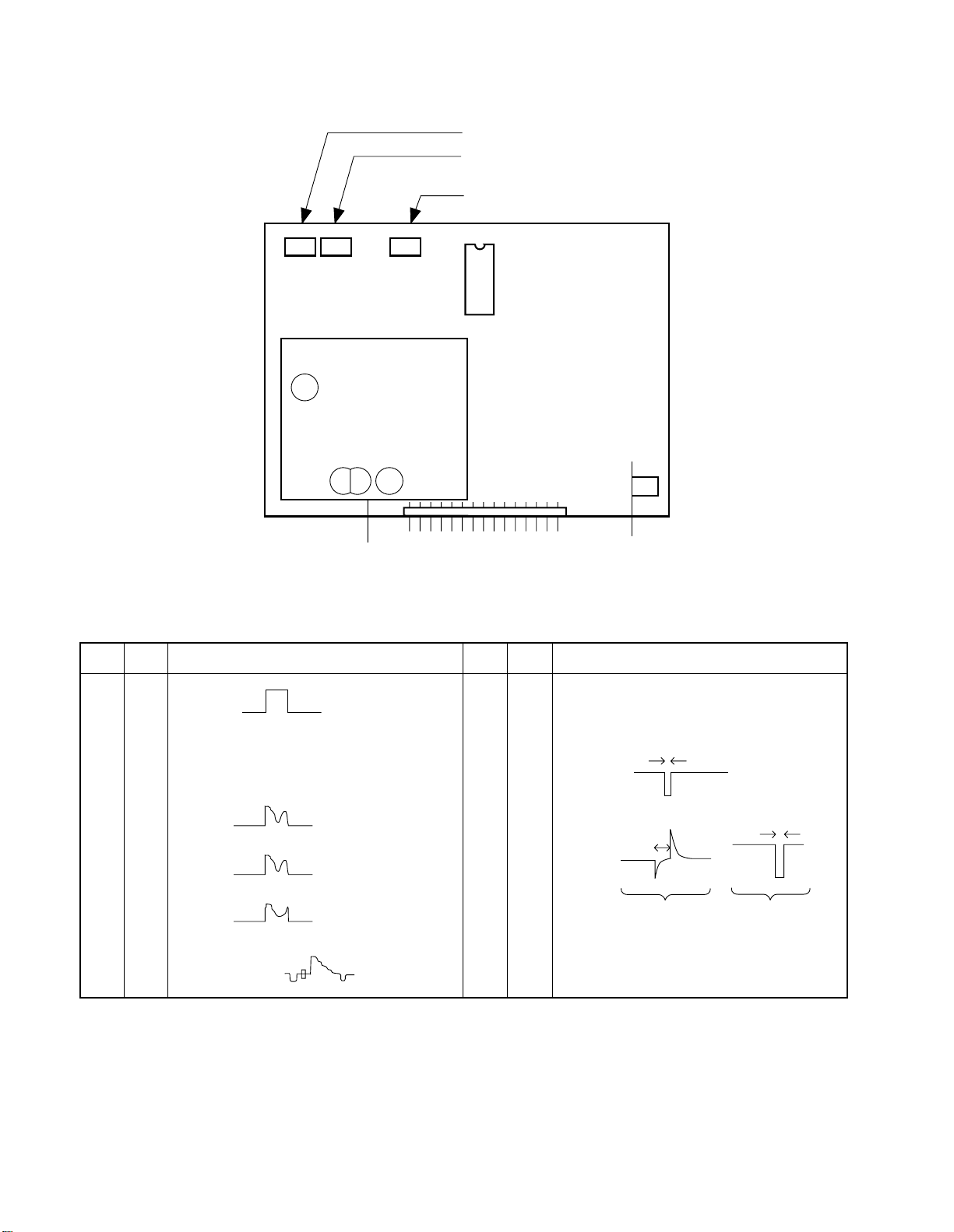
PMUS 02H (SN:23148232)
2
V
3.0V
10mS
6V
-0.9V
1mS
4.2V
0V
Or
B CHASSIS C CHASSIS
RY54
RY55
B-Y OFFSET
R-Y OFFSET
TINT
RY50
1
4
3
2
6
5
8
7
11
10
9
13
12
15
14
PIN I/O NAME PIN I/O NAME
10YS 9I5V
2 - NC 10 I GND
3 I GND 11 I VD
4 O R OUT 12 I HD
5 O G OUT 13 I/O SCL
6 O B OUT 14 I/O SDA
4V
0V
350mS
V
4.8V
.1V
4.8V
4.1V
4.8V
4.1V
7 I GND 15 - NC
4.8V
8 I PIP VIDEO
.8V
4.2
9-2
Page 76
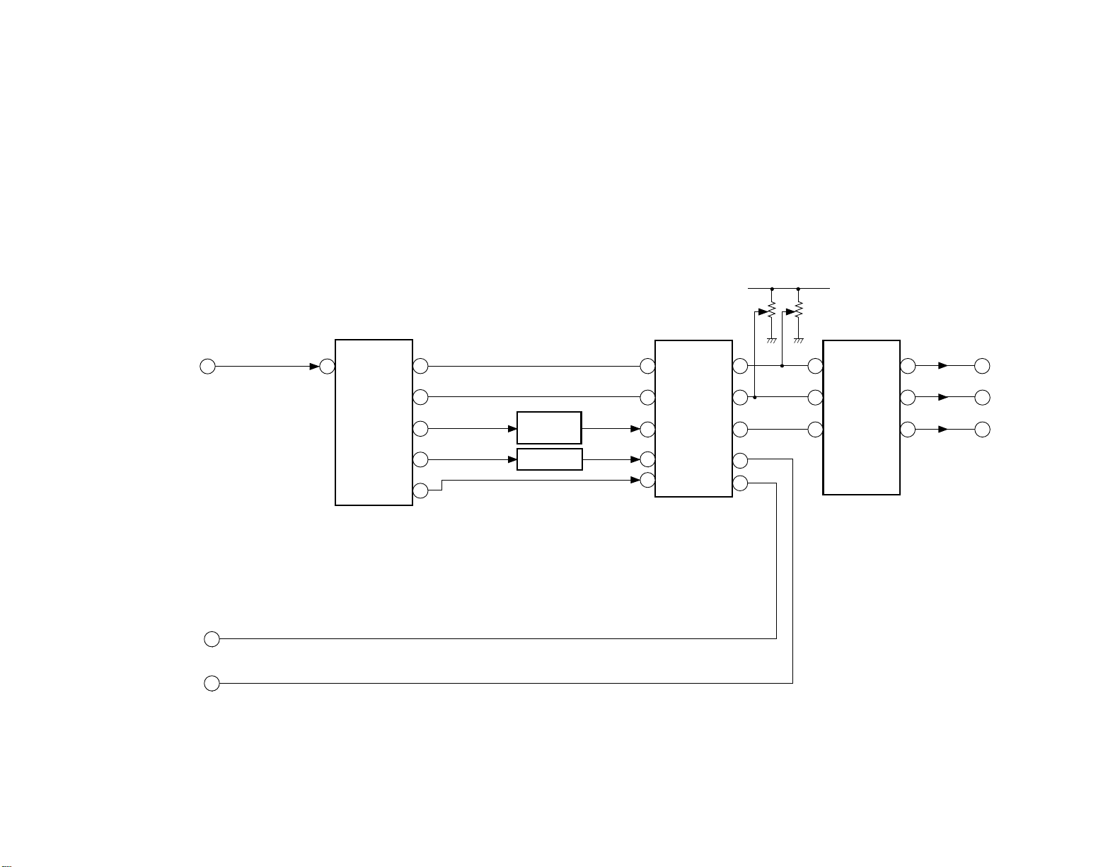
PMUS02H
<BLOCK DIAGRAM OF PIP MODULE>
RY55 RY54
9-3
PIP VIDEO
836
VIDEO
IN
Y-OUT
QY01
PC 1832GT
m
(PIP V/C/D)
VD
11
HD
12
B-Y
OUT
R-Y
OUT
HD
VD
14
13
12
10
11
SLICE
WAVE FORM
MODULATION
51
49
47
78
76
BI
RI
YI
HDCN
VDCN
BO
RO
YO
HDPN
VDPN
QY03
TC9083F
(PIP PROCESSOR)
67
65
64
18
16
19
18
16
B-Y
IN
R-Y
IN
YIN
R OUT
G OUT
B OUT
QY01
PC1832GT
m
(PIP V/C/D)
23
24
25
R OUT
4
G OUT
5
B OUT
6
Page 77

NOTES
9-4
Page 78

SECTION X
SYNC SEPARATION, H-AFC,
H-OSCILLATOR CIRCUITS
10-1
Page 79
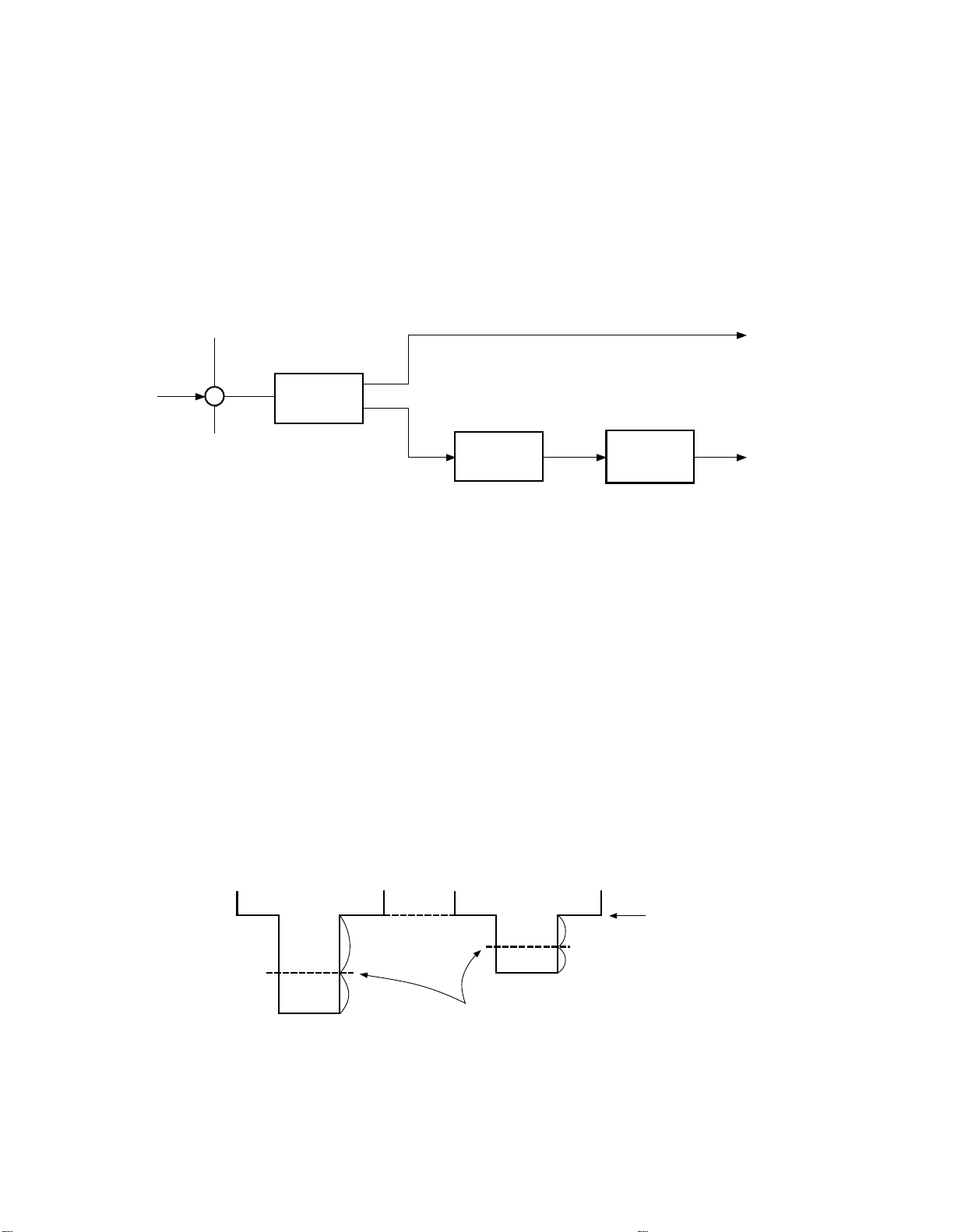
1. SYNC SEPARATION CIRCUIT
The sync separation circuit separates a sync signal from a
video signal and feeds it to an H and V deflection circuits.
The separation circuit consists of an amplitude separation (H
and V sync separation circuit) and a frequency separation
circuit (V sync separation circuit) which performs the
separation by using a frequency difference between H and V.
In the N5SS chassis, all these sync separation circuits are
contained in a V/C/D IC (TA1222N).
Fig. 10-1 shows a block diagram of the sync separation
circuit.
Sync
Composite
video
signal
input
17
Q501
H. V SYNC
SEPARATION
CIRCUIT
Fig. 10-1 Sync separation circuit block diagram
1-1. Theory of Operation 1-1-1. Auto slicer type synchronous separation circuit
When a synchronizing signal is separated, synchronous
separation is made from the beginning with constant voltage
in the conventional synchronous separation circuit. The auto
slider type circuit employed in this time makes synchronous
separation at a constant rate against the synchronizing signal
amplitude. (See Fig. 10-2)
In this method, even if an abnormal signal with small
amplitude is applied, stable synchronizing performance can
be obtained without separating pedestal.
V SYNC
SEPARATION
CIRCUIT
WAVEFORM
SHAPEING
CIRCUIT
H sync siganl
V sync signal
(Reset pulse)
D
B
A
a: Corect Sync. Signal
Sync Separation Level A:B=C:D
b: Small Amplitude Sync. Signal
B
Fig. 10-2 Synchronous separation by auto slider system
10-2
Pedestal Level
Page 80
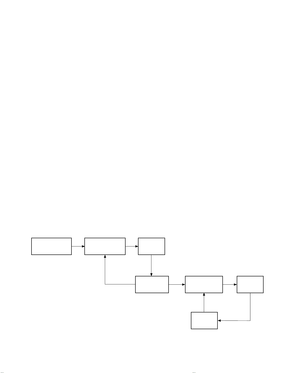
1-1-2. V Sync Separation Circuit
To separate a V sync signal from the composite sync signal
consisting of V and H sync signals mixed, two stages of
integration circuits are provided inside the IC. The circuit
consists of a differential circuit and a Miller integration
circuit, and has following functions.
(1) Removes H sync signal component.
(2) Maintain stable V sync performance for a tape recorded
with a copy guard.
(3) Stabilized V sync performance under special field
conditions (poor field, ghost, sync depressed, adjacent
channel best).
The V sync signal separated in this stage is processed in a
waveform shape circuit and then used as a reset pulse in the
V division circuit as stated later.
2. H AFC (Automatic Frequency Control)
CIRCUIT
A sync system which performs synchronization with each
waveform of the sync signal as performed in a sync system
in the V circuit is called a direct type sync system. However,
if the synchronization for the H oscillator is carried out with
this method, the H oscillator synchronizes with external
noises and the H synchronization will be disturbed. To
prevent this, an output of the H oscillator is compared with
a reference H sync signal to detect deviations of frequency
and phase. The H oscillator is automatically controlled with
the detected output averaged. This circuit is called an AFC
circuit.
In the N4SS chassis, a conventional AFC circuit is not
employed but a new double AFC circuit built-in the TA1222N
is used. Fig. 10-3 shows the AFC circuit and the block
diagram of the circuit.
First, phases of a 32 fH counted-down signal and a H sync
signal contained in broadcasting signal are compared in the
AFCI loop and the loop develops an H pulse signal for the
AFCII loop. That is, when a phase deference 01 exists in
comparison of the phase of fH signal developed by counting
down the 32 fH signal and the phase of H sync signal of the
broadcasting signal, an error signal corresponding to the
phase different is detected and a correction voltage V1
corresponding to the error output is generated. With this
correction voltage, the 32 fH oscillator circuit is controlled.
The correction (control) voltage for the oscillator varies in
direction of positive or negative corresponding to phase
lead or lag of the fH pulse (developed by counting down)
from the H sync signal. As the H oscillator (32 x fH), a
voltage controlled oscillator (VCO), oscillation frequency
and phase of which can be controlled with the control
voltage is used.
Next, an H pulse signal is created from the fH signal counted
down, and the pulse is used instead of the H sync signal in
the AFCII circuit. The AFCII circuit differs in the loop of
the count down circuit and H output circuit.
The AFCII circuit compares phase of a H BLK pulse created
by waveform shaping a AFC pulse from the FBT and a phase
of the H pulse, and detects an error component corresponding
to the phase difference 02 (if exist) and develops a
correction voltage V2 corresponding to the error, thereby
controlling the phase of Q501 H out.
The H output control voltage varies in a positive or negative
direction corresponding to the phase lead or lag of the H
BLK pulse from that of the H pulse. The phase of H out is
varied with the control voltage to make synchronization
with the H pulse phase.
The purpose of the double AFC circuit employed this time
SYNC SEPARATION
CIRCUIT
PHASE DETECTION
CIRCUIT
AFC I LOOP
Fig. 10-3 H AFC circuit block diagram
32 x fH
VCO
H COUNT DOWN
(DIVIDING)
10-3
PHASE DETECTION
CIRCUIT
FBT PULSE
(AFC PULSE)
AFC II LOOP
H DRIVE
H OUTPUT
CIRCUIT
Page 81
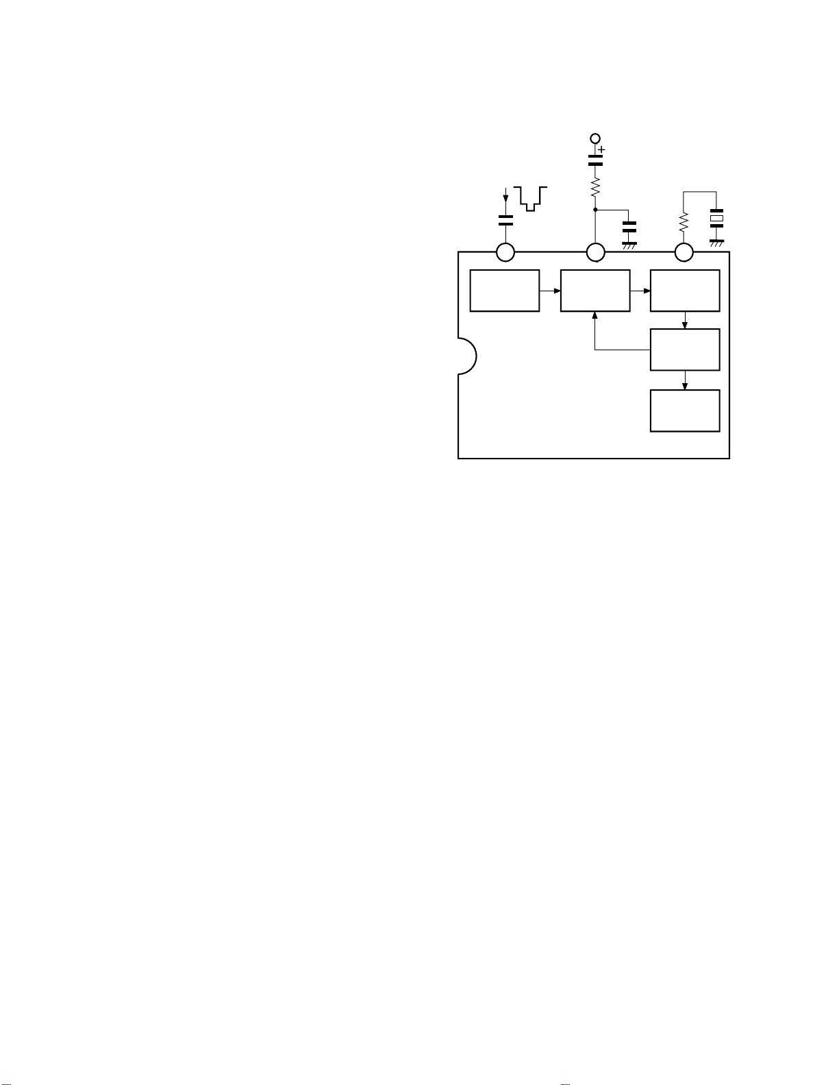
is to improve horizontal jitter under signal reception in a
poor electrical field. The jitter in the poor field strength and
distortion due to phase difference are incompatible. That
is,to improve the jitter under poor field strength, response
speed must be slowed by lowering the AFC sensitivity. On
the other hand, to improve distortion due to the phase
difference, the response must be increased by increasing the
AFC sensitivity.
In a conventional AFC circuit, setting of the sensitivity is
carried out at one part only, so an compromise point for both
characteristics must be found. However, with the double
AFC circuit employed this time, for the jitter the AFCI loop
works best with decreasing the sensitivity and for the phase
distortion the AFCII loop works with increasing the
sensitivity.
SYNC
IN
17
SYNC
SEPARATION
CIRCUIT
2V
H Vcc
P-P
20 21
H AFC I
CIRCUIT
32 x fH
VCO
3. H OSCILLATOR CIRCUIT
3-1. Outline
A 503 kHz (32 x fH) voltage controlled type oscillator with
a ceramic oscillation element is used to generate a clock
pulse and the clock is counted down, thereby obviating the
need of adjustments for both the H and V deflection process
circuit.
3-2. Theory of Operation
(1) The H sync signal used as a reference signal enters
from the sync separation circuit to the AFCI circuit. At
the same time, the fH pulse created by counting down
the 32 x fH pulse generated in the ceramic oscillator
enters the H AFCI circuit. Phase difference between
these two signals enters an integration circuit (low pas
H COUNT
DOWN
H AFC II
CIRCUIT
TA1222N
Fig. 10-4
10-4
Page 82
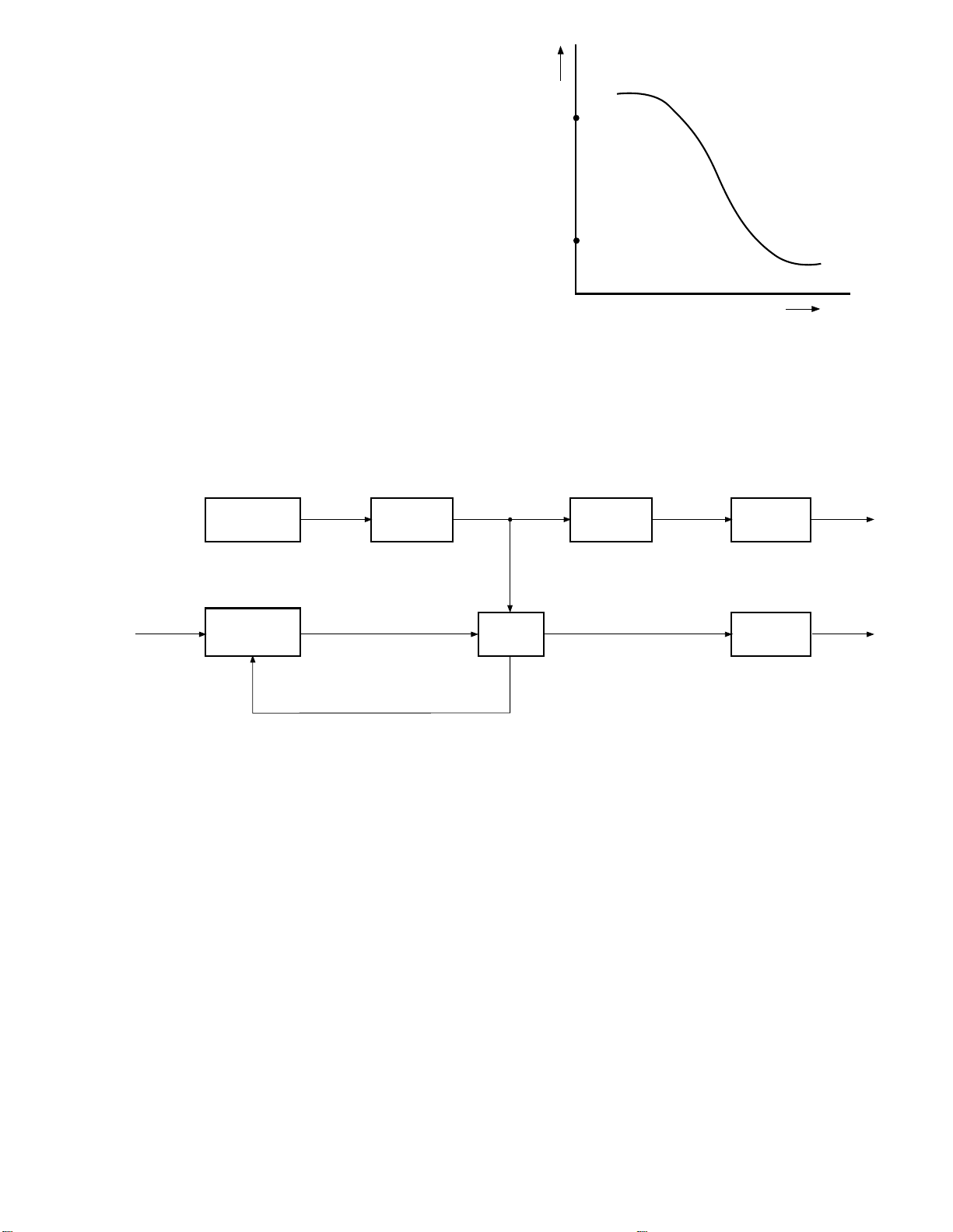
filter) connected to pin 4 and converted into a DC
voltage (AFC voltage).
(2) The AFC voltage controls frequency (32 x fH) of the
oscillator (VCO).
Fig. 10-5 shows the control characteristics of the VCO.
(3) The H output is obtained by dividing the 32 x fH (503
kHz) of the oscillator with flip-flops. Fig. 10-6 shows
the block diagram of this count down circuit.
(4) The V output is created by dividing the 32 x fH
oscillator output into 1/8, and then by counting the 4 x
fH pulse with a vertical counter which is reset with a
V reset pulse (V sync output signal stated under sync
separation).
(5) That is, the V output is not created by simply counting
down the H by performing V synchronization with a V
reset pulse entering within a window provided for V
synchronization --- called direct type sync system,
thus, the circuit can work for non standard signals.
High
OSC frequency (Hz)
Low
Low High
AFC voltage (V)
Fig. 10-5
V sync
signal
32 x fH VCO
V WAVEFORM
SHAPE
CIRCUIT
32fH
X 1/8
Reset
pulse
4fH
V
COUNTER
X 1/4 H OUTPUT
Fig. 10-6 Block diagram of H, V count down circuits
fH
V OUTPUT
10-5
Page 83

NOTES
10-6
Page 84

SECTION XI
VERTICAL OUTPUT CIRCUIT
11-1
Page 85
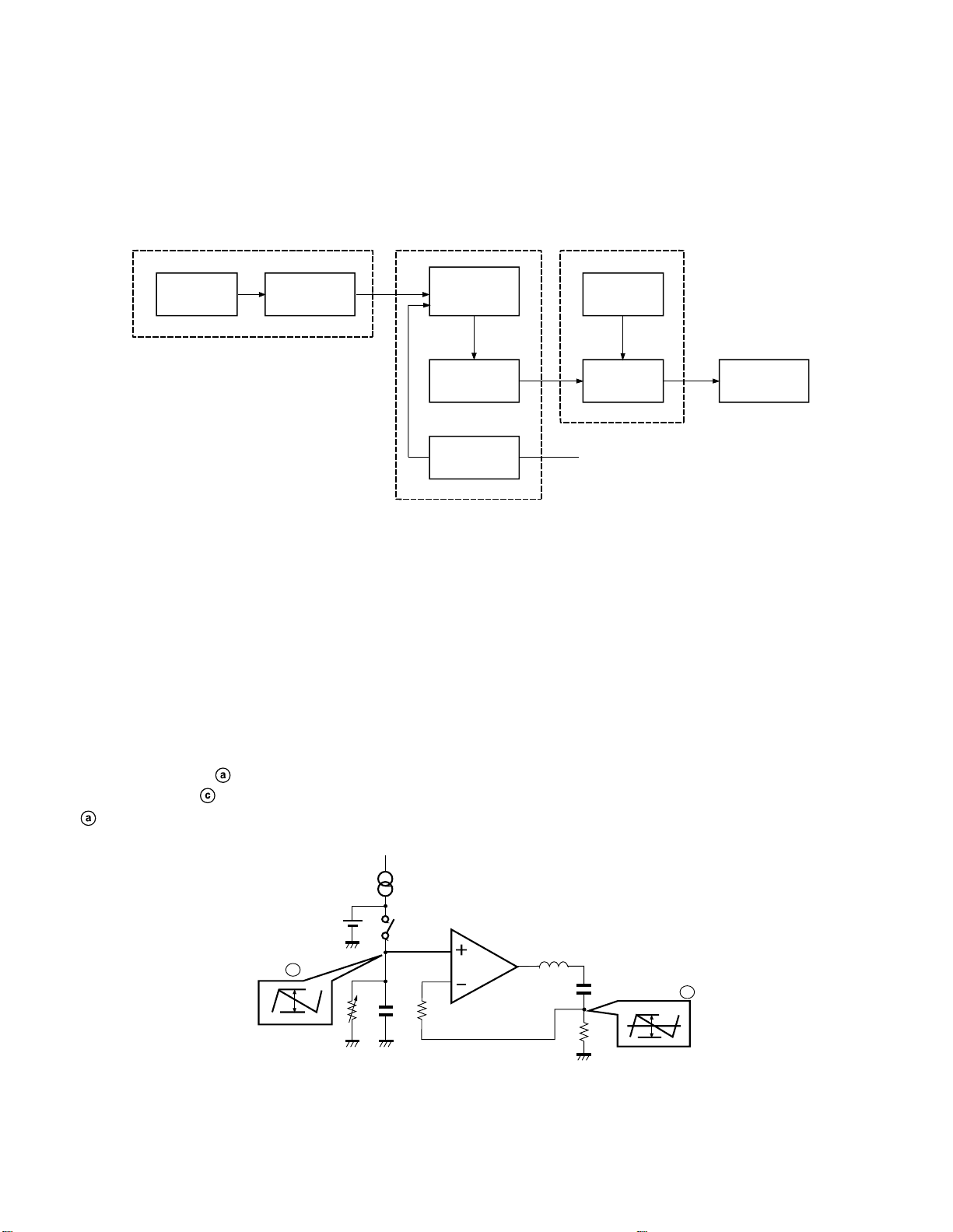
1. OUTLINE
As can be seen from the block diagram, the sync circuit and
the V trigger circuit are contained in Q501 (TA1222N), and
the sawtooth generation circuit and amplifier (V drive circuit)
contained in Q302 (TA8859AP). The output circuit and
pump-up circuit circuits are included in Q301 (TA8427K).
DPS CIRCUIT
Q302 TA8859APQ501 TA1222N
Q301 TA8427K
SYNC
CIRCUIT
V. TRIGGER
Fig. 11-1 Block diagram of V deflection circuit
1-1. Theory of Operation
The purpose of the V output circuit is to provide a sawtooth
wave signal with good linearity in V period to the deflection
yoke.
When a switch S is opened, an electric charge charged up to
a reference voltage VP discharges in an constant current
rate, and a reference sawtooth voltage generates at point a.
This voltage is applied to (+) input (non-inverted input) of
an differential amplifier, A. As the amplification factor of
A is sufficiently high, deflection current flows so that the
voltage V2 at point becomes equal to the voltage at point
.
SAM TOOTH
WAVE GAIN
CIRCUIT
AMP
LOGIC
CIRCUIT
PUMP-UP
CIRCUIT
OUTPUT
Microcomputer
DEFLECTION
YOKE
Vp
a
V1
S: Switch
R1 C2 R2
Differential
amplifier
A
L
C2
R3
c
V2
Fig. 11-2
11-2
Page 86
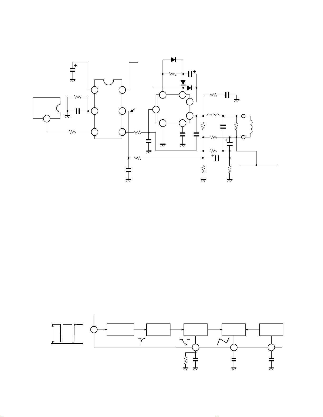
2. V OUTPUT CIRCUIT
2-1. Actual Circuit
Q501
31
C322
R320
R329
C321
7
4
1
D309
R308 C308
D308
6
3
Q301
2
5
C309
C311
D301
R303
L301 R336
R307
R306
R313
C305
R304
C313
C307
R305
L462+L463+L464
C306
+27V
+9V
15
14
Q302
13
3
FEEDBACK
6
8
C319
+35V
R301
C314
R330
Fig. 11- 3
2-2. Sawtooth Waveform Generation 2-2-1. Circuit Operation
The sawtooth waveform generation circuit consists of as
shown in Fig. 11-4. When a trigger pulse enters pin 13, it is
differentiated in the waveform shape circuit and only the
falling part is detected by the trigger detection circuit, to the
waveform generation circuit is not susceptible to variations
of input pulse width.
The pulse generation circuit also works to fix the V ramp
voltage at a reference voltage when the trigger pulse enters,
so it can prevent the sawtooth wave start voltage from
variations by horizontal components, thus improving
interlacing characteristics.
5Vp
DC=0V
13
WAVEFORM
SHAPE
Q302
TRIGGER
DET.
PULSE
GAIN
14
R329 C321 C322 C323
V. RAMP
15 16
+
AGC
Fig. 11-4
11-3
Page 87
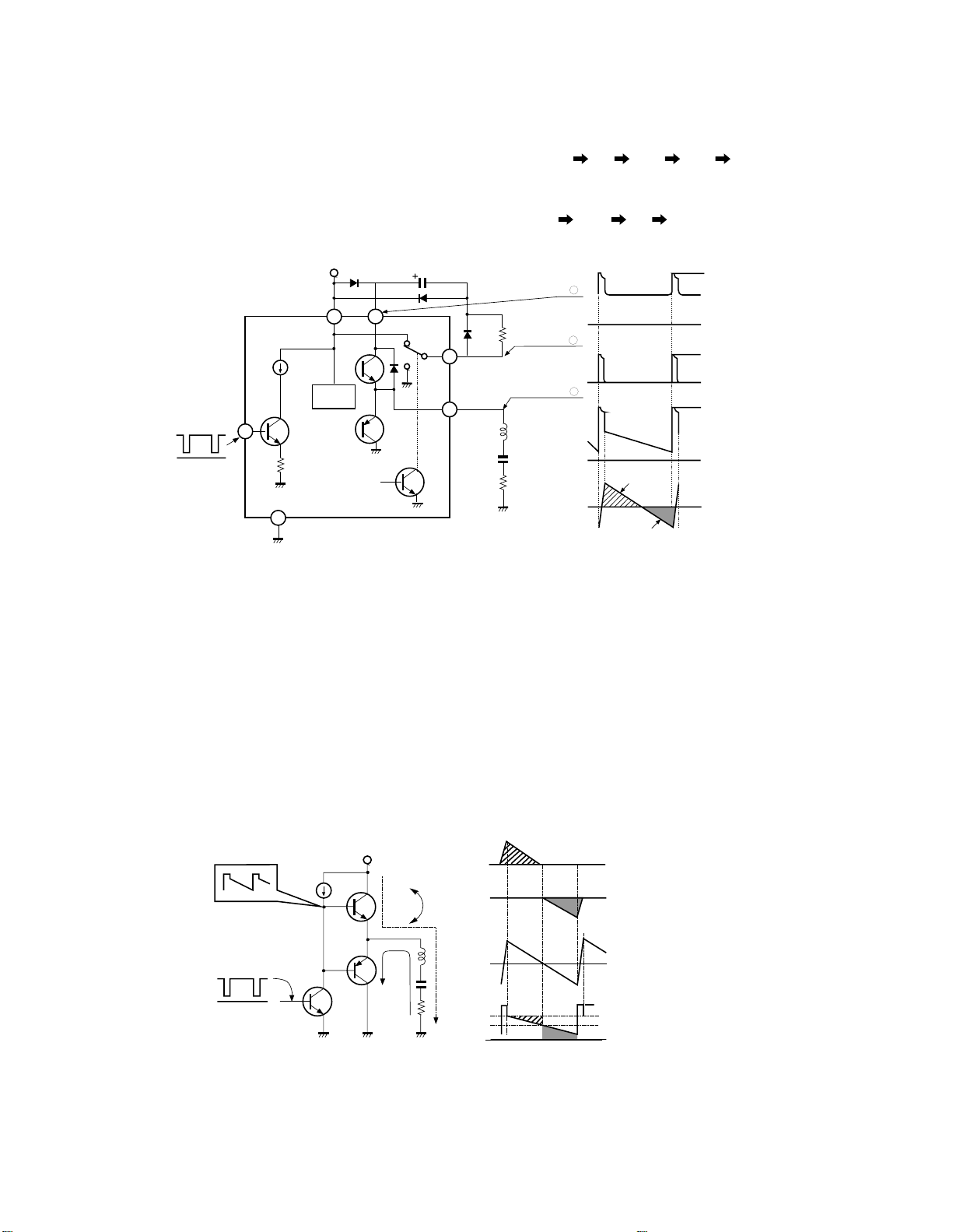
2-3. V Output
(a)
2-3-1. Circuit Operation
The V output circuit consists of a V driver circuit Q302,
Pump-up circuit and output circuit Q301, and external
circuit components.
(1) Q2 amplifies its input fed from pin 4 of Q301, Q3, Q4
output stage connected in a SEPP amplifies the current
+35V
D301 C308
D308
Q301
4
BIAS
Q2
CIRCUIT
1
36
Q3
Q4
7
2
and supplies a sawtooth waveform current to a deflection
yoke. Q3 turns on for first half of the scanning period
and allows a positive current to flow into the deflection
yoke (Q3 DY C306 R305 GND), and Q4 turns
on for last half of the scanning period and allows a
negative current to flow into the deflection yoke
(R305 C306 DY Q4). These operations are
shown in Fig. 11-5.
50V
27V
GND
27V
GND
50V
GND
GND
D309 R308
DY
+
C306
R305
V 3
V 7
V 2
Q3 ON
Q4 ON
Fig. 11-5 V output circuit
(2) In Fig. 11-6 (a), the power Vcc is expressed as a fixed
level, and the positive and negative current flowing
into the deflection yoke is a current (d) = current (b) +
(c) in Fig. 11-6, and the emitter voltage of Q3 and Q4
is expressed as (e).
(3) Q3 collector loss is i1 x Vce1 and the value is equal to
multiplication of Fig. 11-6 (b) and slanted section of
Fig. 11-6 (e), and Q4 collector loss is equal to
multiplication of Fig. 11-6 (c) and dotted section of
Fig. 11-6 (e).
Power Vcc
Q3
i1
Vce 1
Q4
Q2
i2
Basic circuit
GND (b) Q3 Collector current i1
GND (c) Q4 Collector current i2
GND (d) Deflection yoke current i1+i2
Vp
Vcc
(e)
1/2 Vcc
GND
Fig. 11-6 Output stage operation waveform
11-4
Page 88
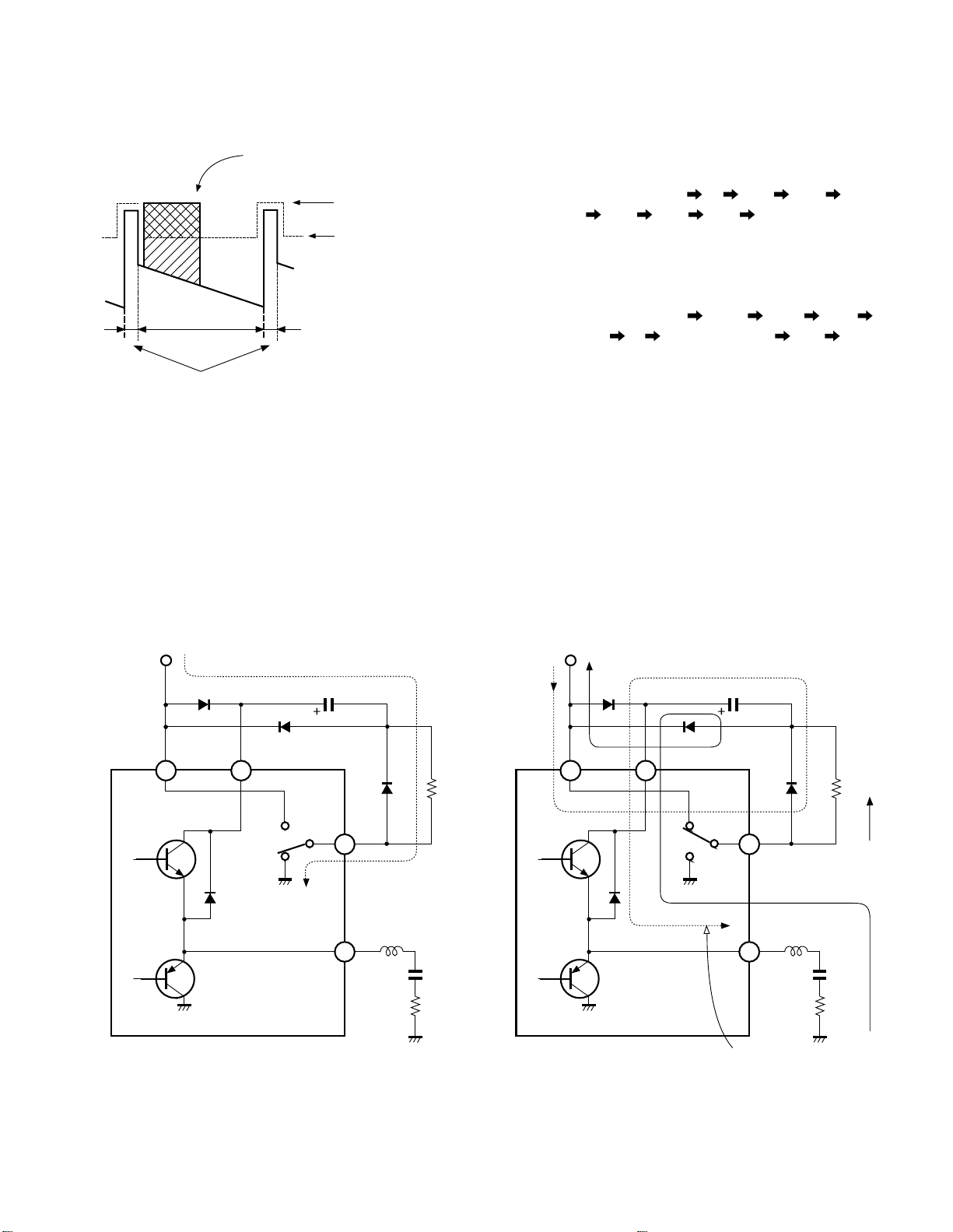
(4) To decrease the collector loss of Q3, the power supply
)
y
(a)
voltage is decreased during scanning period as shown
in Fig. 11-7, and VCE1 decreases and the collector loss
of Q3 also decreases.
Q3 Collector loss decreases
by amount of this area
Power supply
for flyback period (Vp
Power supply
for scanning period
(Vcc)
Scanning period
back period
Fl
Fig. 11-7 Output stage power supply voltage
basic operation is shown in Fig. 11-8.
(6) Since pin 7 of a transistor switch inside Q301 is
connected to the ground for the scanning period, the
power supply (pin 3) of the output stage shows a
voltage of (VCC-VF), and C308 is charged up to a
voltage of (VCC-VF--VR) for this period.
(7) First half of flyback period
Current flows into L462 D1 C308 D308 VCC
(+35V) GND R305 C306 L462+L463+L464
in this order, and the voltage across these is:
VP=VCC+VF+(VCC-VF-VR)+VF about 50V is
applied to pin 3. In this case, D301 is cut off.
(8) Last half of flyback period
Current flows into VCC switch D309 C308
Q301(pin3) Q3 L462+L463+L464 C306 R305
in this order, and a voltage of VP=VCC-VCE (sat)VF+(VCC-VF-VR)-VCE (sat), about 40V is applied
to pin 3.
(9) In this way, a power supply voltage of about 27V is
applied to the output stage for the scanning period and
about 50V for flyback period.
(5) In this way, the circuit which switches power supply
circuit during scanning period and flyback period is
called a pump-up circuit. The purpose of the pump-up
circuit is to return the deflection yoke current rapidly
for a short period (within the flyback period) by
applying a high voltage for the flyback period. The
D301 C308
D308
Q301
6
Q3
Q4
D1
3
D309 R308
Switch
7
L462+L463+L464
2
+
C306
Q301
Q3
Q4
D301 C308
D308
6
3
D1
Switch
D309 R308
7
First half
L462+L463+L464
2
+
C306
VR
R305
Scanning period (b) Flyback period
Last half
R305
Fig. 11-8
11-5
Page 89

2-4. V Linearity Characteristic Correction
2-4-1. S-character Correction
(Up-and Down-ward Extension Correction)
A parabola component developed across C306 is integrated
by R306 and C305, and the voltage is applied to pin 6 of
Q302 to perform S-character correction.
2-4-2. Up-and Down-ward Linearity Balance
A voltage developed at pin 2 of Q301 is divided with
resistors R307 and R303, and the voltage is applied to pin
6 of Q301 to improve the linearity balance characteristic.
Moreover, the S-character correction, up- and down-ward
balance correction, and M-character correction are also
performed through the bus control.
11-6
Page 90
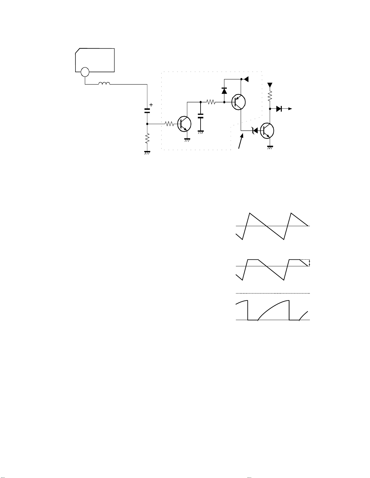
3. PROTECTION CIRCUIT FOR V DEFLECTION STOP
Q301
2
DPC CIRCUIT
L462+L463+L464
VE R TIC A L D EF LE CT IO N C O IL S
C306
Q350
V-NF
R305
R350
0.82
When the deflection current is not supplied to the deflection
coils, one horizontal line appears on the screen. If this
condition is not continued for a long time, no trouble will
occur in a conventional TV. But in the projection TV, all the
electron beams are directly concentrated at the fluorescent
screen because of no shadow mask used, and burns out the
screen instantly.
To prevent this, the stop of the V deflection is detected when
the horizontal one line occurs, and the video signals are
blanked out so that the electron beams are not emitted.
When the V deflection circuit is operating normally, a
sawtooth wave voltage is obtained across (R305), so Q350
repeats on-off operation in cycle of V sync. In this case, the
collector voltage of Q35 is set to develop less than (12V-VBE
(Q351)) with R352 and C350 as shown in Fig. 4-8.
Accordingly, Q351 and Q353 are continuously turned on. As
a result, diode D354 is turned off, giving no influence on the
blanking operation.
Next, when the V deflection stops, the voltage across (R305)
does not develop, so Q350 turns off, and both the Q351 and
Q353 are turned off. Then, the picture blanking terminal pin
13 of ICA05 is set to high through R354 and D354 connected
to 90V power line, BLANKING CIRCUIT ON thus cutting
off the projection tubes.
Fig. 11-9
D350
R352
C350
olttage Across
Q350 BASE
Q351 Collector
Q351
R305
12V
D353
V-STOP
9V
R354
D354
Q353
Fig. 11-10
BLANKING
CIRCUIT
Q340 V
12V-V
BE
BE
(Q341)
11-7
Page 91
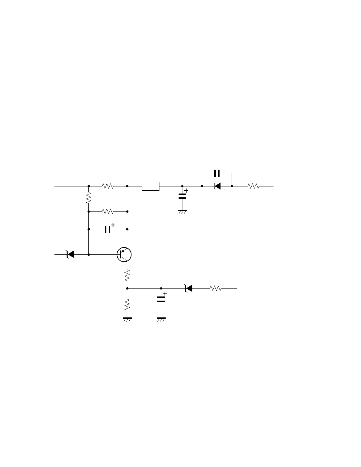
3-1. +35V Over Current Protection Circuit
6
The over current protection circuit cuts off the power supply
relay when it detects abnormal current increased in the +35V
power line due to failure of the vertical deflection circuit.
3-1-1. Theory of operation
Fig. 11-11 shows the circuit diagram of the over current
protection circuit. When the load current of the +35V line
increases, the voltage across a resistor of T370 will also
increase. When the voltage increases across R370. and the
voltage developed across R371 becomes higher than the Vbs
of Q370, Q370 turns on and a voltage develops across R374
due to the collector current flowing. When this voltage
increases to a value higher than about 13V, Z801 operates,
thus cutting off the power relay. When the circuit operates,
a power LED provided will turn on and off in red.
C303
R372
D421
UZ22BSD
R370
R371
C370
R373
R374
+35V
Q370
2SA933SQ
D370
UZ11BSB
C371
Fig. 11-11
C310
D302
R375
R327
FBT
pin
To pin 14 (GATE)
of Z801
11-8
Page 92

SECTION XII
HORIZONTAL DEFLECTION CIRCUIT
12-1
Page 93
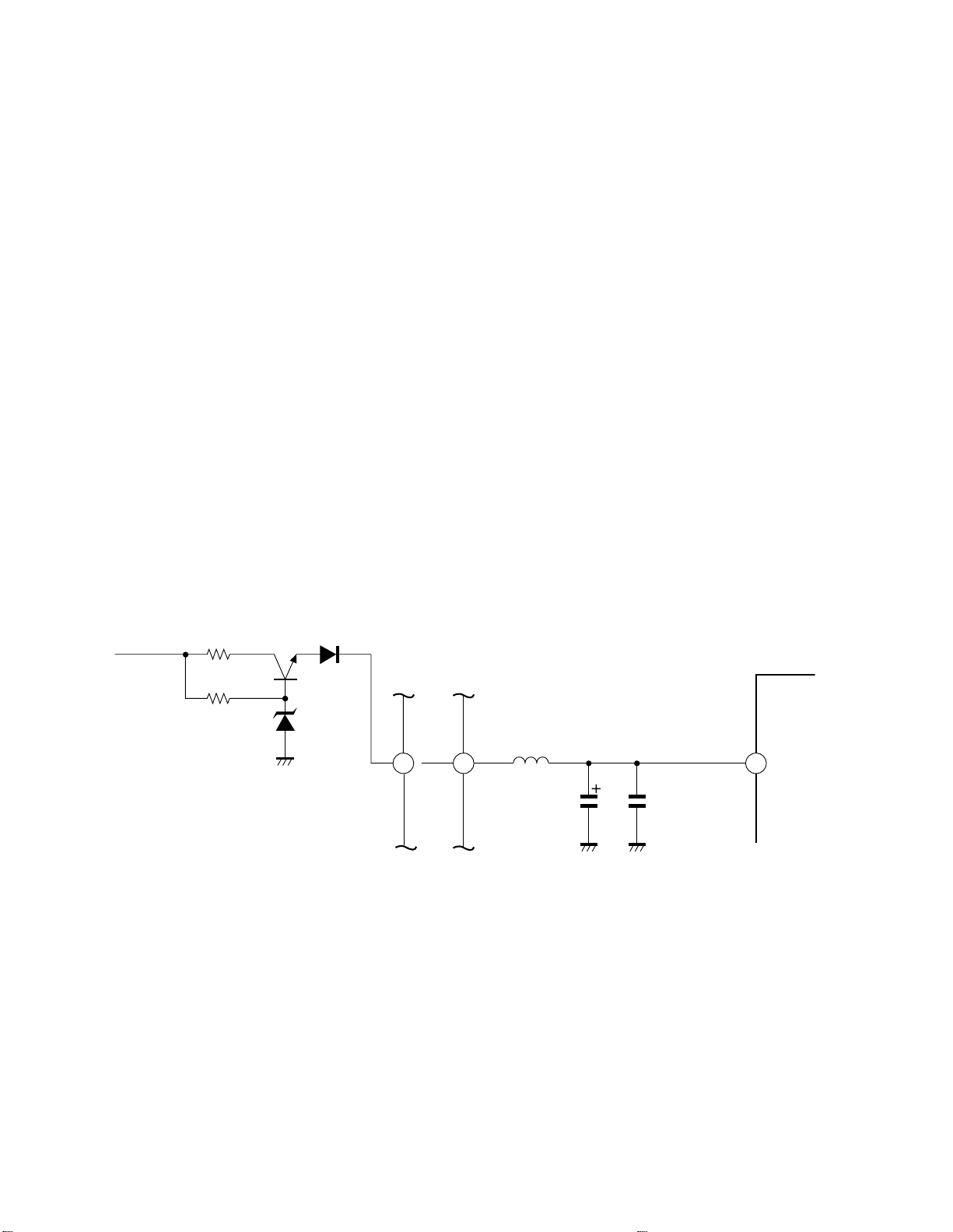
1. OUTLINE
The H deflection circuit works to deflect a beam from left to
right by flowing a sawtooth waveform of 15.734 kHz into the
DY H deflection coil.
2. HORIZONTAL DRIVE CIRCUIT
The H drive circuit works to start the H output circuit by
applying HVCC (Q501 DEF power source) to pin 22 of Q501
(TA1222N) and a bias to the H drive transistor Q402 at the
main power on.
2-1. Theory of Operation
(1) When the power switch is on, the main power supply of
125V starts to rise. At the same time, AF power supply
25V also rises.
(2) With 25V line risen, Q430 base voltage which is created
by dividing the audio power with R433 and D430 also
rises. Then, the transistor Q430 turns on and the HVCC
is applied from the audio power line through R432 and
D431 to pin 22 of Q501.
R432 Q430 D431
R433
D430
BB81
81
BB80
81 22
SIGNAL
L400
C431 C430
Fig. 12-1 H drive circuit block diagram
Q501
H Vcc
12-2
Page 94
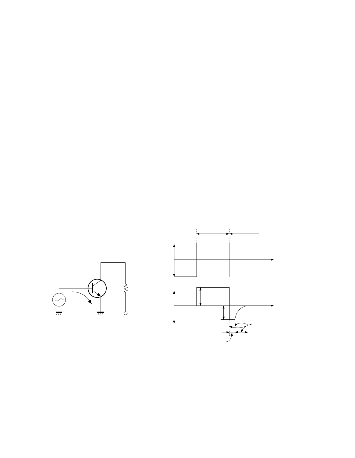
3. BASIC OPERATION OF HORIZONTAL
)
DRIVE
A sufficient current must flow into base of the horizontal
output transistor to rapidly make it into a saturated (ON)
condition or a cut off (OFF) condition. For this purpose, a
drive amplifier is provided between the oscillator circuit and
the output circuit to amplify and to waveshape the pulse
voltage.
3-1. Theory of Operation
(1) The horizontal drive circuit works as a so called switching
circuit which applies a pulse voltage to the output
transistor base and makes the transistor on when the
voltage swings in forward direction and off in reverse
direction.
(2) To turn on the output transistor completely and to make
the internal impedance low, a sufficiently high, forward
drive voltage must be applied to the base and heavy base
current ib must be flown. On the contrary, to completely
turn off the transistor, a sufficiently high, reverse voltage
must be applied to the base.
(3) When the transistor is on (collector current is maximum)
condition with the sufficiently high forward voltage
applied to the base, the transistor can not be turned off
immediately, if a reverse base bias is applied to the base
because minority carriers storaged in the base can not be
reduced to zero instantly. That is, a reverse current
flows through an external circuit and gradually reduces
to zero. The time lag required for the base current to
disappear is called a storage time and falling time.
(4) To shorten the storage time and the falling time, a
sufficiently high reverse bias voltage must be applied to
allow a heavy reverse current to flow. This operation
also stabilizes operation of the horizontal output
transistor.
On period OFF period
+
0
-
+
ib
0
V
(a)
-
Forward
current
Reverse
current
Falling
time
Storage
time
t Input waveform (b
t Base current (c)
Fig. 12-2
12-3
Page 95
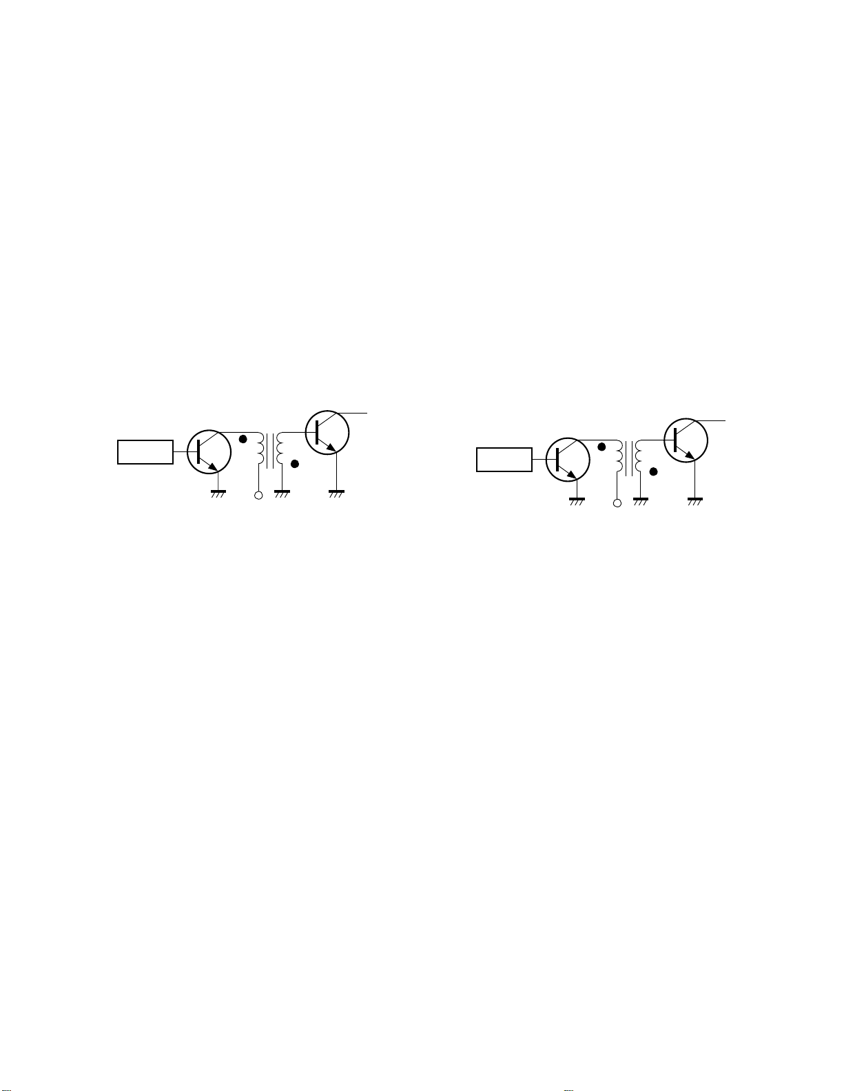
3-2. Drive System 3-2-1. ON drive system
When the drive transistor is on, the horizontal output transistor
also turns on.
Merit:
• The base current can be precisely controlled without
being affected by variation of pulse width which is
caused by the horizontal oscillator circuit and the drive
circuit.
Demerit:
• It is difficult to flow a reverse bias current to the horizontal
output transistor to eliminate its storage carrier for transient
period of on to off period for the horizontal output
transistor.
3-2-2. OFF drive system
When the drive transistor is on, the horizontal output transistor
is off.
Merit:
• Energy balance between on and off periods of the drive
circuit is better, and the circuit can be simplified.
• Reverse base current of the horizontal output transistor
can be controlled easily.
Demerit:
• Base-emitter forward current flowing into the horizontal
output transistor is susceptible to on-period variation of
the drive transistor.
H OSC
H driver
ON
(OFF)
Fig. 12-3
+B
H output
ON
(OFF)
H OSC
H driver
ON
(OFF)
Fig. 12-4
+B
H output
ON
(OFF)
12-4
Page 96
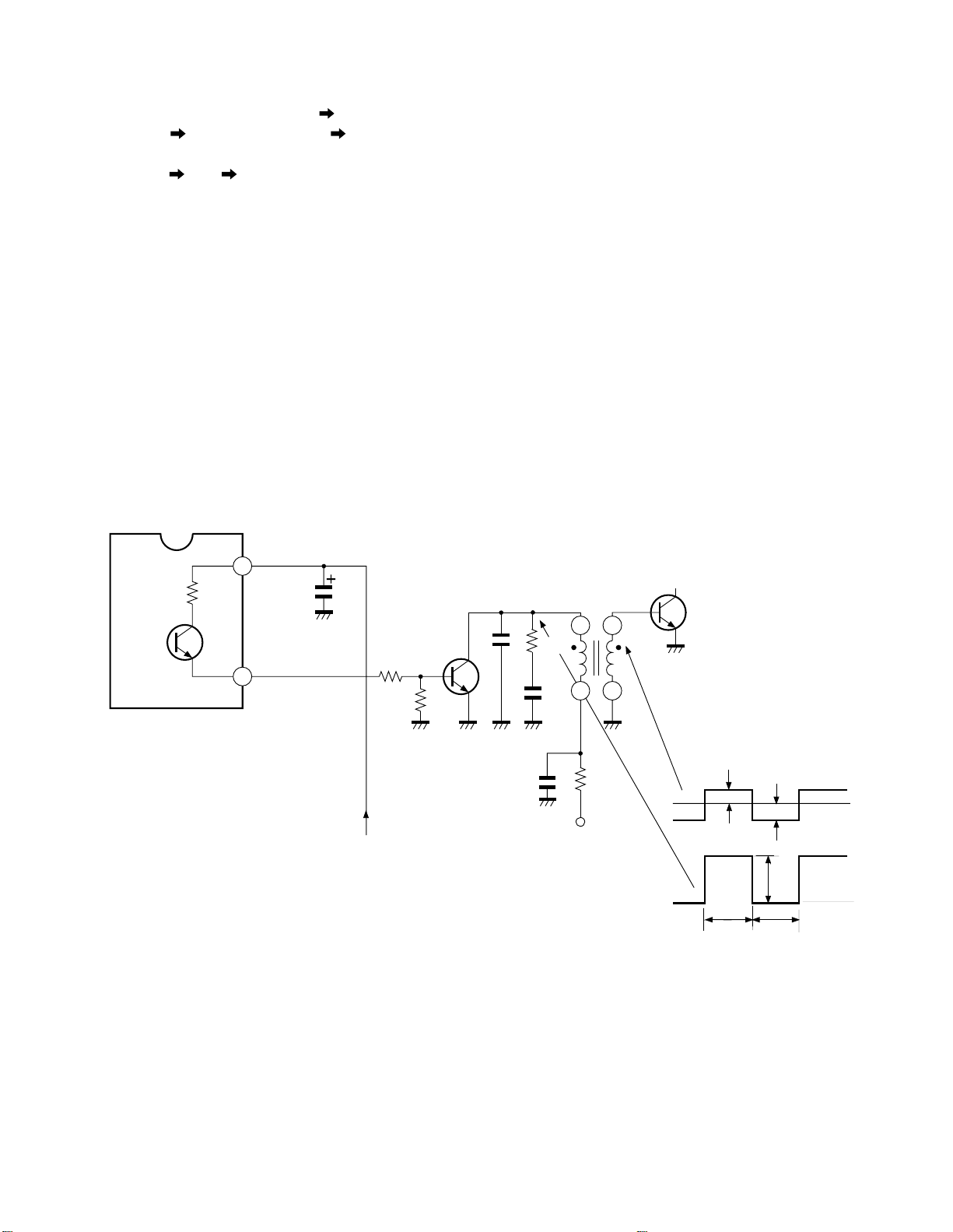
3-3. Circuit Description
V
In the N5SS chassis, the off drive system is employed.
(1) When Q1 inside Q501 is turned on, Q402 base is
forward biased through 9 V pin 22 of Q501 (H.
VCC) pin 23 of Q501 (H. Out) R411/R410 resistor
divider, and then, Q402 collector current flows through
125V R416 T401. In this case, the H output
transistor Q404 turns on with the base-emitter reverse
biased because of the off drive system employed.
(2) On the contrary, when Q1 inside IC501 is off (pin 8 is
0V), base-emitter bias of Q402 becomes 0V and Q402
turns off, and a collector pulse as shown in Fig. 12-5
develops at the collector.
The voltage is stepped down and Q404 is forward
biased with this voltage, thus turning on Q404.
(3) In this way, by stepping down the voltage developed at
primary winding of the drive transformer and by applying
it to Q404, a sufficient base current flows into Q404
base, thereby switching the Q404.
Q501
Q1
22
23
H. Vcc
C431
9V
R411
R410
C417
Q402
H drive
transistor
R415
C413
+
C416
T401
H drive
transistor
1
2
R416
+125V
3
Q404
H output
4
transistor
Q402
V1
OFF
V2
0V
VCP
0
Q402
ON
Fig. 12-5
12-5
Page 97
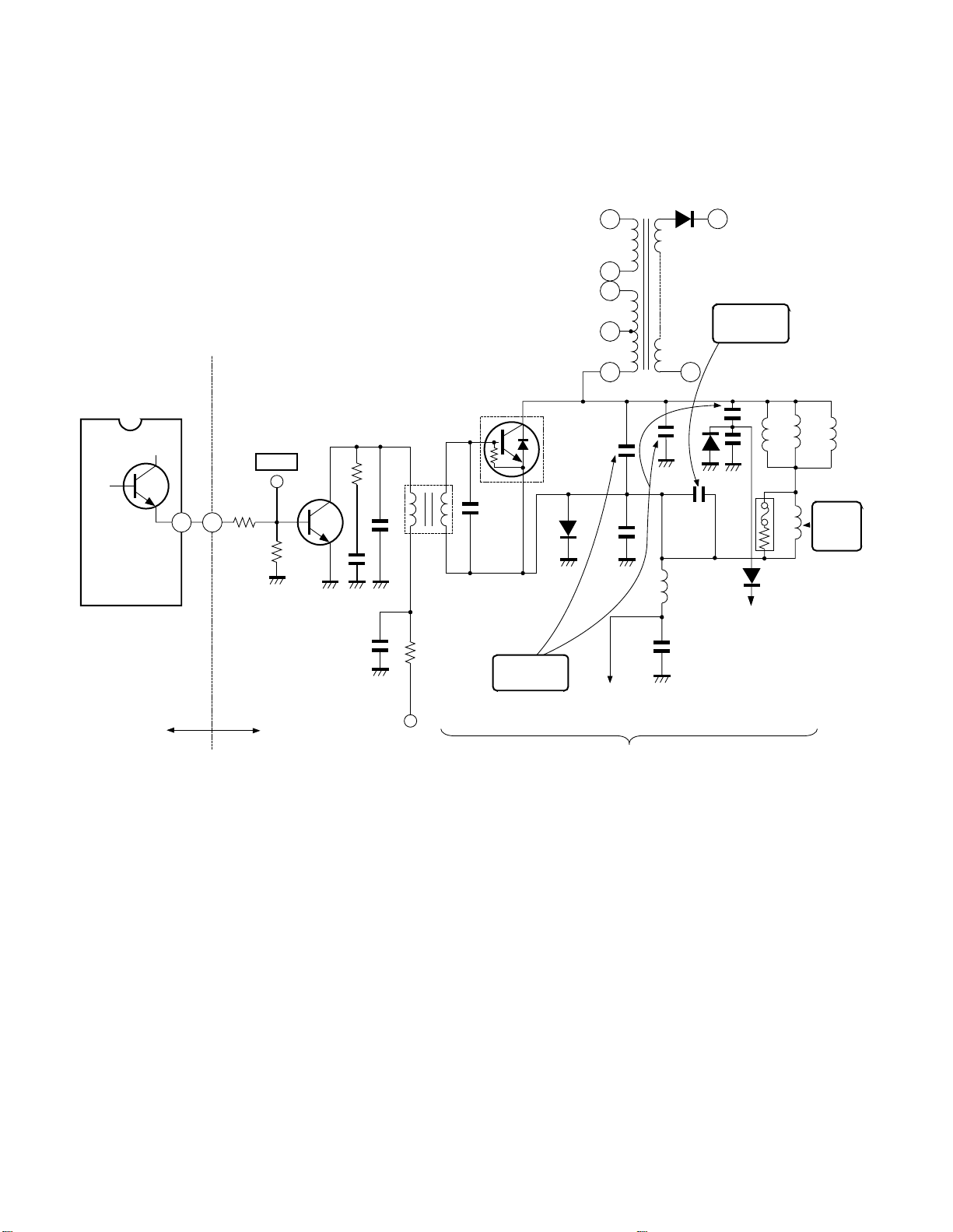
4. HORIZONTAL OUTPUT CIRCUIT
The horizontal output circuit applies a 15.734 kHz sawtooth
wave current to the deflection coil with mutual action of the
horizontal output transistor and the damper diode, and deflects
the electron beam from left to right in horizontal direction.
IC501
H. out
Q1
23
83
BB81
R411
R410
TP-33
Q402
H drive
R415
C413
C416
T401
H drive
transformer
C417
+
Q404
H output
(With damper diode)
C463
R416
Resonat
capacitor
C444
D461
C467
To DPC output
10
5
2
3
1
C440
C464
HV
T461
FBT
S-charactor
capacitor
8
C343
D444
L461
+
Deflection yoke
C418
C423
D443
To High Voltage
Regulator Circuit
(H coil)
L462
R441
L441
L463
L464
H
linearity
coil
SIGNAL DEF/POWER PCB
PCB
125V
Diode modulator circuit
Fig. 12-6
12-6
Page 98
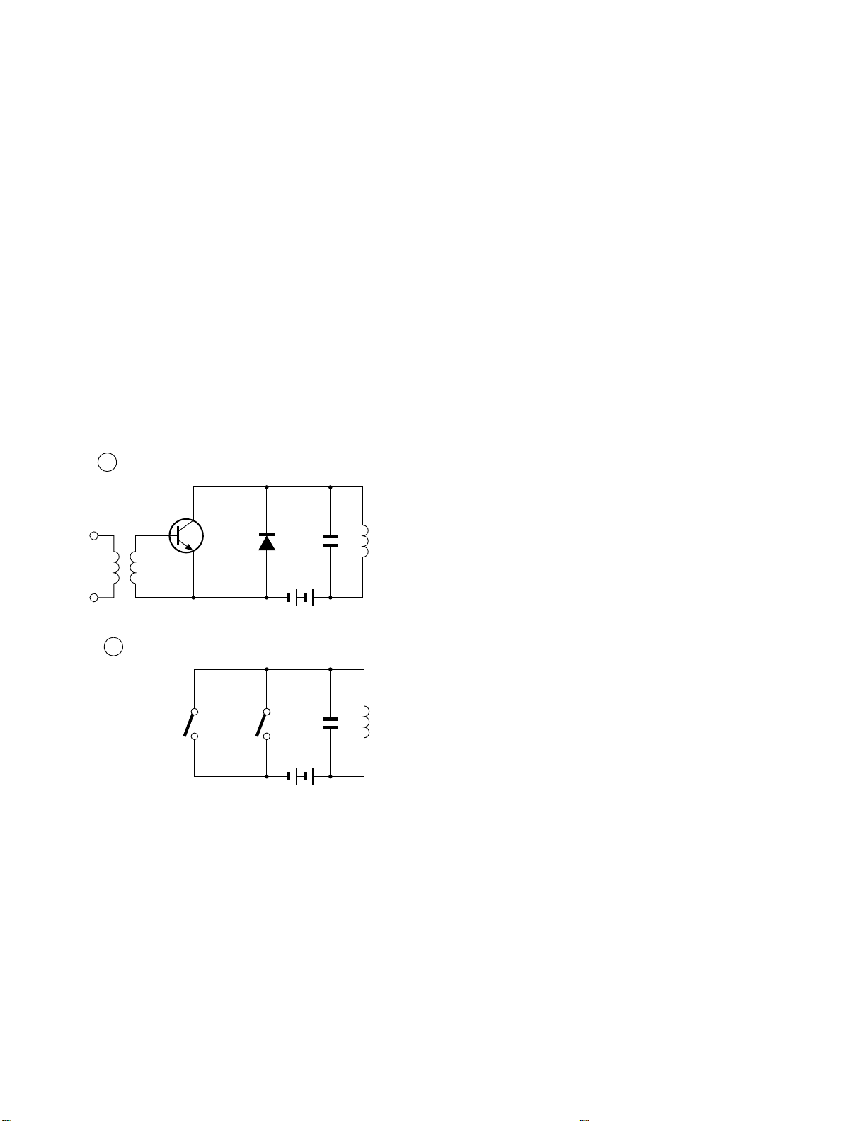
4-1. Theory of Operation 4-1-1. Operation of Basic Circuit
(1) To perform the horizontal scanning, a 15.734 kHz
sawtooth wave current must be flown into the horizontal
deflection coil. Theoretically speaking, this operation
can be made with the circuit shown in Fig. 12-7 a and b.
(2) As the switching operation of the circuit can be replaced
with switching operation of a transistor and a diode, the
basic circuit of the horizontal output can be expressed
by the circuit shown in Fig. 12-7 a. That is, the transistor
can be turned on or off by applying a pulse across the
base emitter. A forward switching current flows for onperiod, and a reverse switching current flows through
the diode for off-period. This switching is automatically
carried out. The diode used for this purpose is called a
damper diode.
a H output basic circuit
H output
transistor
b H output equivalent circuit
DCo
Damper
diode
Resonant
capacitor
Vcc
L
Deflection
yoke
Description of the basic circuit
1. t1~t2:
A positive pulse is applied to base of the output transistor
from the drive circuit, and a forward base current is flowing.
The output transistor is turned on in sufficient saturation
area. As a result, the collector voltage is almost equal to the
ground voltage and the deflection current increases from
zero to a value in proportionally. (The current reaches
maximum at t2, and a right half of picture is scanned up to this
period.)
2. t2:
The base drive voltage rapidly changes to negative at t2 and
the base current becomes zero. The output transistor turns
off, collector current reduces to zero, and the deflection
current stops to increase.
3. t2~t3:
The drive voltage turns off at t2, but the deflection current
can not reduce to zero immediately because of inherent
nature of the coil and continues to flow, gradually decreasing
by charging the resonant capacitor C0. At the same time, the
capacitor voltage or the collector voltage is gradually
increases, and reaches maximum voltage when the deflection
current reaches zero at t3. Under this condition, all electromagnetic energy in the deflection coil at t2 is transferred to
the resonant capacitor in a form of electrostatic energy.
4. t3~t4:
Since the charged energy in the resonant capacitor discharges
through the deflection coil, the deflection current increases
in reverse direction, and voltage at the capacitor gradually
reduces. That is, the electrostatic energy in the resonant
capacitor is converted into a electromagnetic energy in this
process.
SW1
SW2
Fig. 12-7
Vcc
Co
L
5. t4:
When the discharge is completed, the voltage reduces to
zero, and the deflection current reaches maximum value in
reverse direction. The t2~t4 is the horizontal flyback period,
and the electron beam is returned from right end to the left
end on the screen by the deflection current stated above. The
operation for this period is equivalent to a half cycle of the
resonant phenomenon with L and C0, and the flyback period
is determined by L and C0.
12-7
Page 99
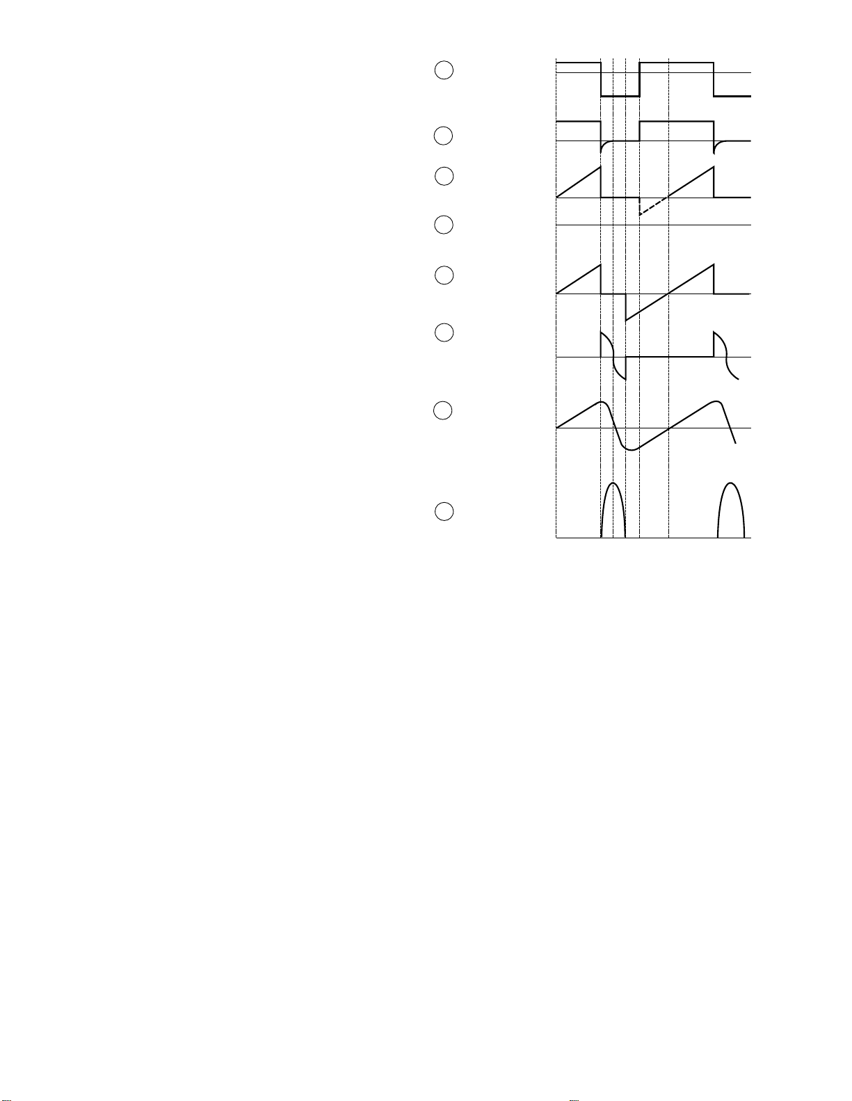
6. t4~t6:
g
For this period. C0 is charged with the deflection current
having opposite polarity to that of the deflection current
stated in "3.", and when the resonant capacitor voltage
exceeds VCC, the damper diode D conducts. The deflection
current decreases along to an exponential function
(approximately linear) curve and reaches zero at t6. Here,
operation returns to the state described under "1.", and the
one period of the horizontal scanning completes. For this
period a left half of the screen is scanned.
In this way, in the horizontal deflection scanning, a current
flowing through the damper diode scans the left half of the
screen; the current developed by the horizontal output
transistor scans the right half of the screen; and for the
flyback period, both the damper diode and the output transistor
are cut off and the oscillation current of the circuit is used.
Using the oscillation current improves efficiency of the
circuit. That is, about a half of deflection current (one fourth
in terms of power) is sufficient for the horizontal output
transistor.
TR
A
base voltage
TR
B
base current
TR
C
collector
current
D
D
damper
current (SW2)
E
Switch
current
(TR, SW1)
F
Resonant
capacitor
current (Co)
G
Deflection
current (Lo)
t1 t2 t3 t4 t5 t6
0
0
0
0
0
0
0
H
TR
collector
e
volta
0
Fig. 12-8
12-8
Page 100
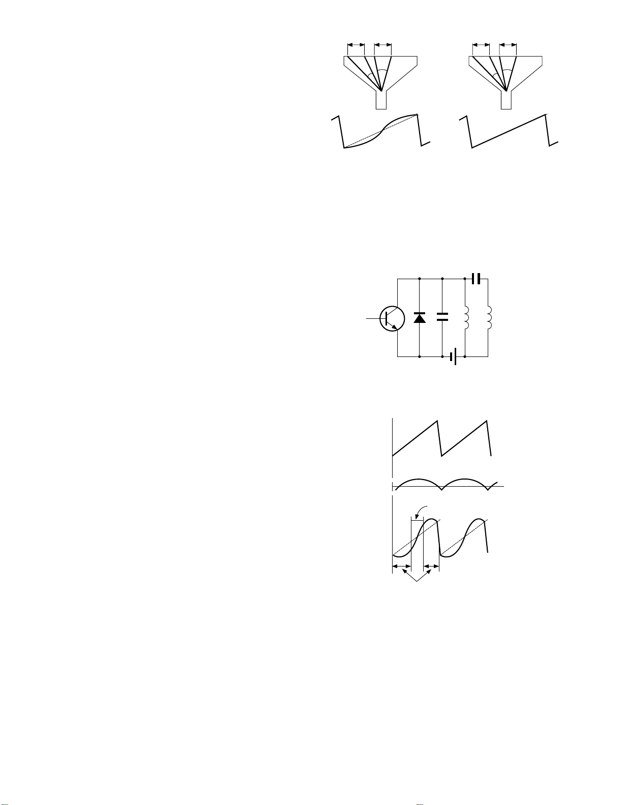
(d) Sy
Amplitude Correction
To vary horizontal amplitude, it is necessary to vary a
sawtooth wave current flowing into the deflection coil.
These are two methods to vary the current; a method which
varies LH by connecting a variable inductance L in series with
the deflection yoke, and a method which varies power supply
voltage (across S-character capacitor) for the deflection
yoke.
As the DPC circuits is used in the this chassis, the later
method which varies the deflection yoke power supply
voltage by modifying the bus data is used.
4-1-2. Linearity Correction (LIN)
(1) S-curve Correction (S Capacitor)
Pictures are expanded at left and right ends of the screen even
if a sawtooth current with good linearity flows in the deflection
coil when deflection angle of a picture tube increases. This is
because projected image sizes on the screen are different at
screen center area and the circumference area as shown in
Fig. 12-9. To suppress this expansion at the screen
circumference, it is necessary to set the deflection angle q1
to a large value (rapidly deflecting the electron beam) at the
screen center area, and to set the deflection angle q2 to a
small value (scanning the electron beam slowly) at the
circumference area as shown in Fig. 12-9.
In the horizontal output circuit shown in Fig. 12-10, capacitor
CS connected in series with the deflection coil LH is to block
DC current. By properly selecting the value of CS and by
generating a parabolic voltage developed by integrating the
deflection coild current across the S capacitor, and by varying
the deflection yoke voltage with the voltage, the scanning
speed is decreased at beginning and end of the scanning, and
increased at center area of the screen. The S curve correction
is carried out in this way, thereby obtaining pictures with
good linearity.
t2
t1
q
q
2
1
(a) S-character correction (b)
t2 = t1
<
q
2
q
1
t2
Fig. 12-9
Cs
TR
D Co
Vcc
(a) H output circuit
(b) Sawtooth wave current
(c) Voltage across LH
Fast deflection
t1
q
q
2
L
H
Deflection coil
1
t2 > t1
=
q
2
q
1
Slow deflection
nthesized current
Fig. 12-10
12-9
 Loading...