

Page 1

FILE NO. 140-200221
SERVICE MANUAL
COLOR TELEVISION/
DVD VIDEO PLAYER
MD20FM3
Page 2
CA UTION
THIS DIGITAL VIDEO PLAYER EMPLOYS A LASER SYSTEM.
TO ENSURE PROPER USE OF THIS PRODUCT, PLEASE READ THIS SERVICE MANUAL CARE-
FULLY AND RETAIN FOR FUTURE REFERENCE. SHOULD THE UNIT REQUIRE MAINTENANCE,
CONTACT AN AUTHORIZED SERVICE LOCATION-SEE SERVICE PROCEDURE.
USE OF CONTROLS, ADJUSTMENTS OR THE PERFORMANCE OF PROCEDURES OTHER THAN
THOSE SPECIFIED HEREIN MAY RESULT IN HAZARDOUS RADIATION EXPOSURE.
TO PREVENT DIRECT EXPOSURE TO LASER BEAM, DO NOT TRY TO OPEN THE ENCLOSURE.
VISIBLE LASER RADIATION MAY BE PRESENT WHEN THE ENCLOSURE IS OPENED. DO NOT
STARE INTO BEAM.
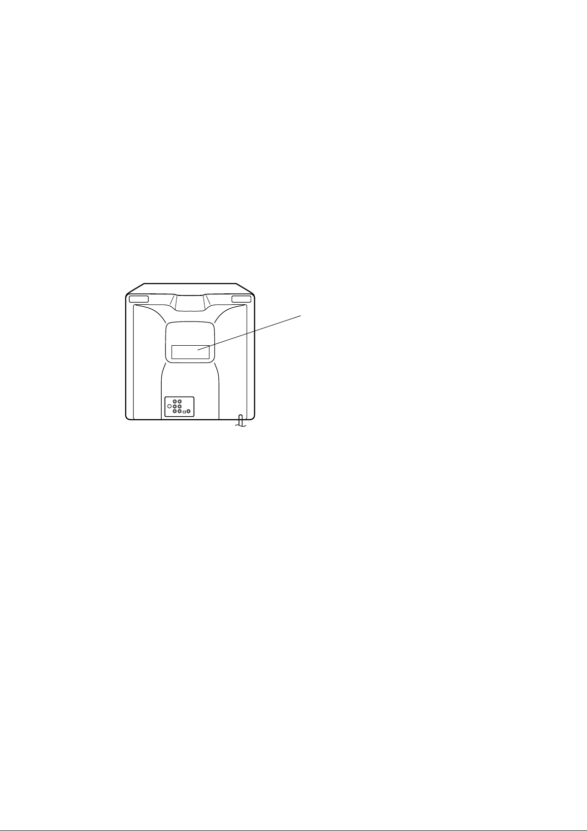
Location of the required Marking
The rating sheet and the safety caution are on the rear of the unit.
CERTIFICATION: COMPLIES WITH FDA
RADIATION PERFORMANCE STANDARDS,
21 CFR SUBCHAPTER J.
A1-1
Page 3
SERVICING NOTICES ON CHECKING
As for the places which need special attentions,
they are indicated with the labels or seals on the
cabinet, chassis and parts. Make sure to keep the
indications and notices in the operation manual.
2. AVOID AN ELECTRIC SHOCK
There is a high voltage part inside. Avoid an
electric shock while the electric current is
flowing.
3. USE THE DESIGNATED PARTS
The parts in this equipment have the specific
characters of incombustibility and withstand
voltage for safety. Therefore, the part which is
replaced should be used the part which has
the same character.
Especially as to the important parts for safety
which is indicated in the circuit diagram or the
table of parts as a mark, the designated
parts must be used.
4. PUT PARTS AND WIRES IN THE
ORIGINAL POSITION AFTER
ASSEMBLING OR WIRING
There are parts which use the insulation
material such as a tube or tape for safety, or
which are assembled in the condition that
these do not contact with the printed board.
The inside wiring is designed not to get closer
to the pyrogenic parts and high voltage parts.
Therefore, put these parts in the original
positions.
5. TAKE CARE TO DEAL WITH THE
CATHODE-RAY TUBE
In the condition that an explosion-proof cathoderay tube is set in this equipment, safety is
secured against implosion. However, when
removing it or serving from backward, it is
dangerous to give a shock. Take enough care to
deal with it.
6. AVOID AN X-RAY1. KEEP THE NOTICES
Safety is secured against an X-ray by considering about the cathode-ray tube and the high
voltage peripheral circuit, etc.
Therefore, when repairing the high voltage peripheral circuit, use the designated parts and
make sure not modify the circuit.
Repairing except indicates causes rising of high
voltage, and it emits an X-ray from the cathoderay tube.
PERFORM A SAFETY CHECK AFTER
7.
SERVICING
Confirm that the screws, parts and wiring which
were removed in order to service are put in the
original positions, or whether there are the
portions which are deteriorated around the
serviced places serviced or not. Check the
insulation between the antenna terminal or
external metal and the AC cord plug blades.
And be sure the safety of that.
(INSULATION CHECK PROCEDURE)
1.
Unplug the plug from the AC outlet.
2.
Remove the antenna terminal on TV and turn
on the TV.
3.
Insulation resistance between the cord plug
terminals and the eternal exposure metal
[Note 2] should be more than 1M ohm by
using the 500V insulation resistance meter
[Note 1].
4.
If the insulation resistance is less than 1M
ohm, the inspection repair should be
required.
[Note 1]
If you have not the 500V insulation
resistance meter, use a Tester.
[Note 2]
External exposure metal: Antenna terminal
Earphone jack
HOW TO ORDER PARTS
Please include the following informations when you order parts. (Particularly the VERSION LETTER.)
1. MODEL NUMBER and VERSION LETTER
The MODEL NUMBER can be found on the back of each product and the VERSION LETTER can be
found at the end of the SERIAL NUMBER.
2. PART NO. and DESCRIPTION
You can find it in your SERVICE MANUAL.
A1-2
Page 4

IMPORTANT SAFEGUARDS
1.
READ INSTRUCTIONS
All the safety and operating instructions should be read before the unit is operated.
2.
RETAIN INSTRUCTIONS
The safety and operating instructions should be retained for future reference.
3.
HEED WARNINGS
All warnings on the unit and in the operating instructions should be adhered to.
4.
FOLLOW INSTRUCTIONS
All operating and use instructions should be followed.
5.
CLEANING
Unplug this unit from the wall outlet before cleaning. Do not use liquid cleaners or aerosol cleaners. Use a damp cloth for cleaning.
6.
ATTACHMENTS
Do not use attachments not recommended by the unit’s manufacturer as they may cause hazards.
7.
WATER AND MOISTURE
Do not use this unit near water. For example, near a bathtub, washbowl, kitchen sink, or laundry tub, in a wet basement, or near a
swimming pool.
8.
ACCESSORIES
Do not place this unit on an unstable cart, stand, tripod, bracket, or table. The unit may fall,
causing serious injury, and serious damage to the unit. Use only with a cart, stand, tripod,
bracket, or table recommended by the manufacturer.
8A.
An appliance and cart combination should be moved with care. Quick stops, excessive force,
and uneven surfaces may cause the appliance and cart combination to overturn.
9.
VENTILATION
Slots and openings in the cabinet and in the back or bottom are provided for ventilation, to ensure reliable operation of the unit, and
to protect it from overheating. These openings must not be blocked or covered. The openings should never be blocked by placing
the unit on a bed, sofa, rug, or other similar surface. This unit should never be placed near or over a radiator or heat source. This
unit should not be placed in a built-in installation such as a bookcase or rack unless proper ventilation is provided or the manufacturer’s instructions have been adhered to.
10.
POWER SOURCES
This unit should be operated only from the type of power source indicated on the rating plate. If you are not sure of the type of
power supply to your home, consult your appliance dealer or local power company. For units intended to operate from battery
power, or other sources, refer to the operating instructions.
11.
GROUNDING OR POLARIZATION
This unit is equipped with a polarized alternating-current line plug (a plug having one blade wider than the other). This plug will fit
into the power outlet only one way. This is a safety feature. If you are unable to insert the plug fully into the outlet, try reversing the
plug. If the plug should still fail to fit, contact your electrician to replace your obsolete outlet. Do not defeat the safety purpose of the
polarized plug. If your unit is equipped with a 3-wire grounding-type plug, a plug having a third (grounding) pin, this plug will only fit
into a grounding-type power outlet. This too, is a safety feature. If you are unable to insert the plug into the outlet, contact your
electrician to replace your obsolete outlet. Do not defeat the safety purpose of the grounding-type plug.
12.
POWER-CORD PROTECTION
Power-supply cords should be routed so that they are not likely to be walked on or pinched by items placed upon or against them,
paying particular attention to cords at plugs, convenience receptacles, and the point where they exit from the appliance.
13.
LIGHTNING
To protect your unit from a lightning storm, or when it is left unattended and unused for long periods of time, unplug it from the wall
outlet and disconnect the antenna or cable system. This will prevent damage to the unit due to lightning and power line surges.
14.
POWER LINES
An outside antenna system should not be located in the vicinity of overhead power lines or other electric light or power circuits, or
where it can fall into such power lines or circuits. When installing an outside antenna system, extreme care should be taken to keep
from touching such power lines or circuits, as contact with them might be fatal.
15.
OVERLOADING
Do not overload wall outlets and extension cords, as this can result in a risk of fire or electric shock.
16.
OBJECT AND LIQUID ENTRY
Do not push objects through any openings in this unit, as they may touch dangerous voltage points or short out parts that could
result in fire or electric shock. Never spill or spray any type of liquid into the unit.
17.
OUTDOOR ANTENNA GROUNDING
If an outside antenna or cable system is connected to the unit, be sure the antenna or cable system is grounded so as to provide
some protection against voltage surges and built-up static charges. Section 810 of the National Electrical Code, ANSI/NFPA 70,
provides information with respect to proper grounding of the mast and supporting structure, grounding of the lead-in wire to an
antenna discharge unit, size of grounding conductors, location of antenna discharge unit, connection to grounding electrodes, and
requirements for the grounding electrode.
18.
SERVICING
Do not attempt to service this unit yourself as opening or removing covers may expose you to dangerous voltage or other hazards.
Refer all servicing to qualified service personnel.
PORTABLE CART WARNING
(symbol provided by RETAC)
S3126A
A1-3
Page 5

IMPORTANT SAFEGUARDS (CONTINUED)
DAMAGE REQUIRING SERVICE
19.
Unplug this unit from the wall outlet and refer servicing to qualified service personnel under the following conditions:
a.
When the power-supply cord or plug is damaged.
b.
If liquid has been spilled, or objects have fallen into the unit.
c.
If the unit has been exposed to rain or water.
d.
If the unit does not operate normally by following the operating instructions. Adjust only those controls that are covered by
the operating instructions, as an improper adjustment of other controls may result in damage and will often require extensive
work by a qualified technician to restore the unit to its normal operation.
e.
If the unit has been dropped or the cabinet has been damaged.
f.
When the unit exhibits a distinct change in performance, this indicates a need for service.
REPLACEMENT PARTS
20.
When replacement parts are required, be sure the service technician uses replacement parts specified by the manufacturer or
those that have the same characteristics as the original parts.
Unauthorized substitutions may result in fire, electric shock or other hazards.
SAFETY CHECK
21.
Upon completion of any service or repairs to this unit, ask the service technician to perform safety checks to determine that the unit
is in proper operating condition.
WALL OR CEILING MOUNTING
22.
The product should be mounted to a wall or ceiling only as recommended by the manufacturer.
HEAT
23.
The product should be situated away from heat sources such as radiators, heat registers, stoves, or other products (including
amplifiers) that produce heat.
DISC TRAY
24.
Keep your fingers well clear of the disc tray as it is closing. It may cause serious personal injury.
CONNECTING
25.
When you connect the product to other equipment, turn off the power and unplug all of the equipment from the wall outlet. Failure
to do so may cause an electric shock and serious personal injury. Read the owner's manual of the other equipment carefully and
follow the instructions when making any connections.
SOUND VOLUME
26.
Reduce the volume to the minimum level before you turn on the product. Otherwise, sudden high volume sound may cause hearing
or speaker damage.
SOUND DISTORTION
27.
Do not allow the product output distorted sound for a longtime. It may cause speaker overheating and fire.
HEADPHONES
28.
When you use the headphones, keep the volume at a moderate level. If you use the headphones continuously with high volume
sound, it may cause hearing damage.
LEASER BEAM
29.
Do not look into the opening of the disc tray or ventilation opening of the product to see the source of the laser beam. It may cause
sight damage.
DISC
30.
Do not use a cracked, deformed, or repaired disc. These discs are easily broken and may cause serious personal injury and
product malfunction.
NOTE TO CATV SYSTEM INSTALLER
31.
This reminder is provided to call the CATV system installer’s attention to Article 820-40 of the NEC that provides guidelines for
proper grounding and, in particular, specifies that the cable ground shall be connected to the grounding system of the building, as
close to the point of cable entry as practical.
EXAMPLE OF ANTENNA GROUNDING AS PER THE NATIONAL ELECTRICAL CODE
GROUND CLAMP
ELECTRIC SERVICE
EQUIPMENT
NEC-NATIONAL ELECTRICAL CODE
S2898A
ANTENNA LEAD IN WIRE
ANTENNA DISCHARGE UNIT
(NEC SECTION 810-20)
GROUND CLAMPS
GROUND CLAMPS
POWER SERVICE GROUNDING ELECTRODE SYSTEM
(NEC ART 250, PART H)
A1-4
Page 6
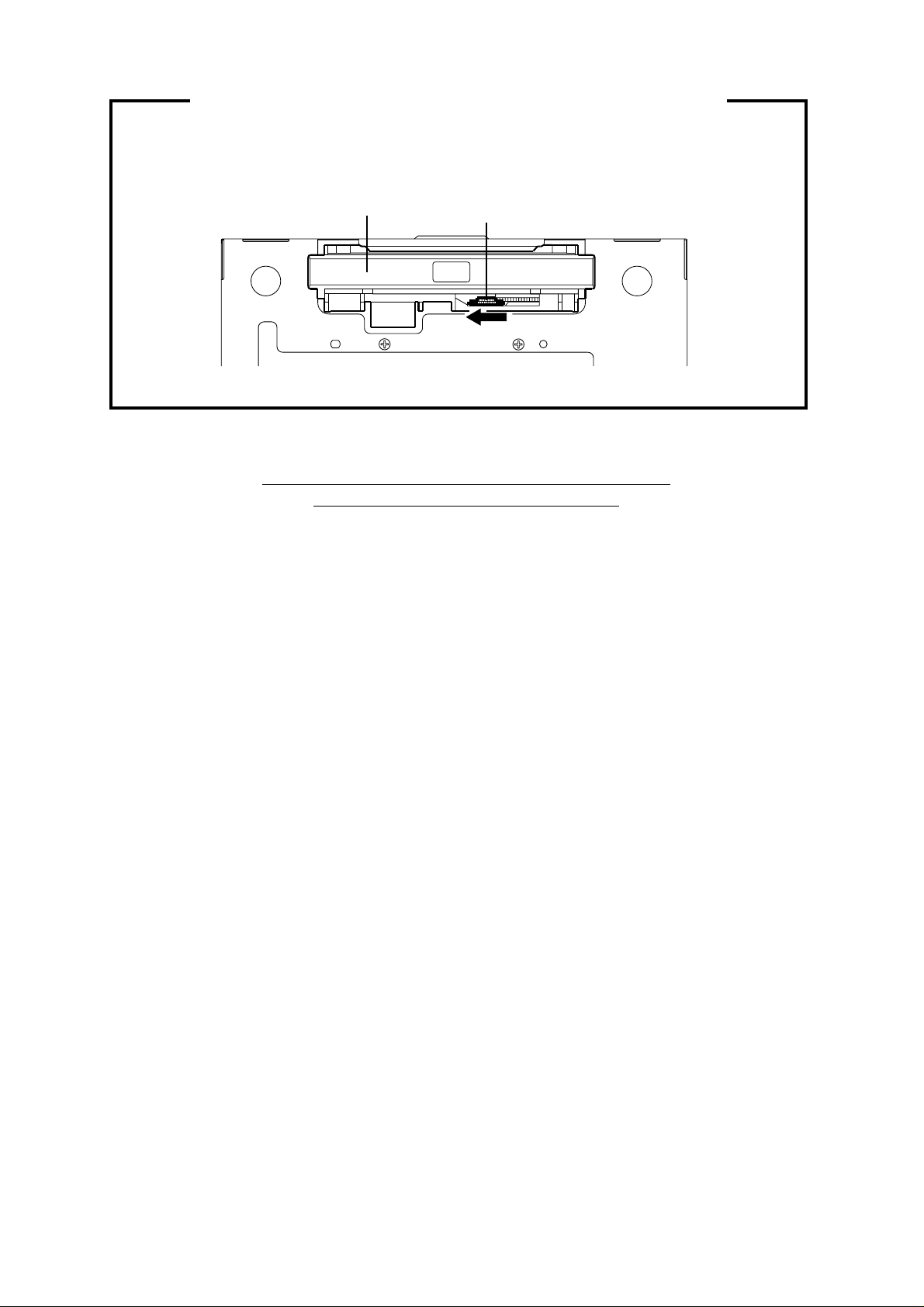
DISC REMOVAL METHOD AT NO POWER SUPPLY
1.2.Remove the Back Cabinet and TV/DVD Block. (Refer to item 1 of the DISASSEMBLY
INSTRUCTIONS.)
Rotate the white gear of Deck CD section in the direction of the arrow by hand, remove the disc from
Deck CD. (Refer to Fig. 1)
Deck CD
Gear (White)
Fig. 1
PARENTAL CONTROL - RATING LEVEL
4 DIGIT PASSWORD CANCELLATION
If the stored 4 digit password in the Rating Level menu needs to be cancelled, please follow the steps below.
Turn Unit ON.
1.
Confirm that no disc on the disc tray.
2.
Press and hold the '7' key on the remote control unit.
3.
Simultaneously press and hold the 'STOP' key on the front panel.
4.
Hold both keys for more than 3 seconds.
5.
The On Screen Display message 'Initialize' will appear.
6.
The 4 digit password has now been cleared.
7.
NB: The above procedure will reset ALL of the player's settings to the default factory state.
A1-5
Page 7

TABLE OF CONTENTS
CAUTION ................................................................................................................................
SERVICING NOTHCES ON CHECKING ...............................................................................
HOW TO ORDER PARTS ......................................................................................................
IMPORTANT SAFEGUARDS.................................................................................................
DISC REMOVAL METHOD AT NO POWER SUPPLY...........................................................
PARENTAL CONTROL-RATING LEVEL ...............................................................................
TABLE OF CONTENTS..........................................................................................................
GENERAL SPECIFICATIONS ...............................................................................................
DISASSEMBLY INSTRUCTIONS
1.REMOVAL OF MECHANICAL PARTS AND P.C. BOARDS ............................................
2.REMOVAL OF ANODE CAP ............................................................................................
3.REMOVAL AND INSTALLATION OF FLAT PACKAGE IC...............................................
SERVICE MODE LIST.............................................................................................................
CONFIRMATION OF HOURS USED ......................................................................................
WHEN REPLACING EEPROM (MEMORY) IC .......................................................................
SERVICING FIXTURES AND TOOLS ....................................................................................
ELECTRICAL ADJUSTMENTS ..............................................................................................
BLOCK DIAGRAMS
TV.........................................................................................................................................
DVD......................................................................................................................................
POWER................................................................................................................................
PRINTED CIRCUIT BOARDS
SYSCON ..............................................................................................................................
AV ........................................................................................................................................
OPEARTION ........................................................................................................................
MAIN/CRT............................................................................................................................
SCHEMATIC DIAGRAMS
MPEG...................................................................................................................................
SDRAM ................................................................................................................................
SYSCON ..............................................................................................................................
VIDEO ENCORDER ............................................................................................................
POWER................................................................................................................................
MICON/TUNER ....................................................................................................................
VIF/SIF/CHROMA ................................................................................................................
SOUND AMP .......................................................................................................................
IN/OUT .................................................................................................................................
AV SW..................................................................................................................................
COMB FILTER .....................................................................................................................
STEREO ..............................................................................................................................
OPERATION ........................................................................................................................
TV POWER ..........................................................................................................................
DEFLECTION ......................................................................................................................
CRT......................................................................................................................................
INTERCONNECTION DIAGRAM ............................................................................................
WAVEFORMS .........................................................................................................................
MECHANICAL EXPLODED VIEW ..........................................................................................
MECHANICAL REPLACEMENT PARTS LIST ......................................................................
ELECTRICAL REPLACEMENT PARTS LIST ........................................................................
A1-1
A1-2
A1-2
A1-3, A1-4
A1-5
A1-5
A2-1
A3-1~A3-6
B1-1, B1-2
B2-1
B3-1, B3-2
C-1
C-1
C-2
C-2
D-1~D-7
E-1, E-2
E-3, E-4
E-5, E-6
F-1, F-2
F-3~F-6
F-7, F-8
F-9, F-10
G-1, G-2
G-3, G-4
G-5, G-6
G-7, G-8
G-9, G-10
G-11, G-12
G-13, G-14
G-15, G-16
G-17, G-18
G-19, G-20
G-21, G-22
G-23, G-24
G-25, G-26
G-27, G-28
G-29, G-30
G-31, G-32
G-33, G-34
H-1~H-4
I-1, I-2
J1-1
J2-1~J2-6
A2-1
Page 8
GENERAL SPECIFICATIONS
G-1 TV CRT CRT Size / Visual Size 20 Inch / 508.0 mmV
G-2 DVD System Color System NTSC
G-3 Tuning Broadcasting System US System M
G-4 Power Power Source AC 120V, 60Hz
G-5 Signal Video Signal Input Level 1 V p-p/75 ohm
System CRT Type FLAT
Deflection 90 degree
Magnetic Field BV/BH +0.45G/0.18G
Color System NTSC
Speaker 2 Speaker
Position Front
Size 3 Inch
Impedance 8 Ohm
Sound Output Max 2.5x2.5 W
10%(Typical) 2.0x2.0 W
Disc
Disc Diameter 120 mm , 80 mm
Deck Disc Loading System Front Loading
Motor 3 Motors
Pick up 1-Lens 2-Beams System
Playback time(Max) DVD 1 DVD 1-Layer 135min (4.7GB)
DVD 2-Layer 245min (8.5GB)
CD 74min
VIDEO CD --min
Search speed Fwd 2-20 times
Actual 2-45 times
Rev 2-20 times
Actual 2-45 times
Slow speed Fwd 1/7-1/2 times
Actual --
Rev 1/7 -1/2 times
Actual 1-2 times
System
Tuner and System 1Tuner
Receive CH Channel Tuner Others
Tuning System F-Synth
Input Impedance VHF/UHF 75 Ohm
CH Coverage
Intermediate Picture(FP) 45.75MHz
Frequency Sound(FS) 41.25MHz
FP-FS 4.50MHz
Preset CH -Stereo/Dual TV Sound Yes
NTSC Playback (PAL60) No
DC -Power Consumption at AC 120W at 120V 60Hz
at DC -Stand by (at AC) 8 W at 120V 60Hz
Per Year -- kWh/Year
Power Supply Cord UL
Protector Power Fuse Yes
Output Level 1 V p-p/75 ohm
S/N Ratio (Weighted) 65dB
Horizontal Resolution at DVD Mode 400 Lines (TV Monitor)
500 Lines ( Video Out)
RGB Signal Output Level -- V p-p/75 ohm
Audio Signal Input Level RCA -8.0dB/50Kohm
Output Level RCA -8.0dB/1Kohm
S/N Ratio at DVD (Weighted) 90 dB
Harmonic Distortion 0.01% (1KHz)
Frequency Response : at DVD 4Hz - 22KHz
at VIDEO CD --
at CD 4Hz - 20KHz
Digital Audio Signal Output Level 0.5 V p-p/75 ohm
DVD Video,CD-DA,CD-R
(CD-DA), CD-RW(CD-DA)
2~69, 4A, A-5~A-1, A~I, J~W,
W+1~W+84
A3-1
Page 9
GENERAL SPECIFICATIONS
G-6 Interface Switch Front Power (Tact) Yes
Rear AC/DC No
Indicator Power Red
Fluorescent Indicator DVD Yes No
Music Calender(1-14,Play) Yes No
Terminals Front Video Input Yes
Rear Video Input(Rear1) Yes
G-7 Set Size Approx. W x D x H (mm) 574x483x514.5
G-8 Weight Net (Approx.) 25.5kg
G-9 Regulation Safety UL
G-10 Temperature Operation 5oC ~ 40oC
G-11 Operating Humidity Less than 80% RH
Channel Up Yes
Channel Down Yes
Volume Up Yes
Volume Down Yes
Play Yes
Open/Close Yes
Skip(>>) Yes
Skip(<<) Yes
Still/Pause No
Stop Yes
Main Power SW No
Color On/Off (SECAM Only) No
Degauss No
Main Power SW No
Stand-by No
On Timer No
Pause Yes No
Track Yes No
-B Yes No
VIDEO Yes No
CD Yes No
Play Yes No
ALL Yes No
PROG Yes No
Mic Mark Yes No
Title Yes No
Repeat Yes No
PBC Yes No
Angle Yes No
Chapter Yes No
A Yes No
7-seg Digit(9) Yes No
Audio Input Yes (Stereo)
Other Terminal Head Phone
Video Input(Rear2) No
Audio Input(Rear1) Yes (Stereo)
Audio Input(Rear2) No
Video Output Yes
Audio Output Yes (Stereo)
Euro Scart No
Digital Audio Output Coaxial
Optical Audio Output No
Color Stream No
Diversity No
Ext Speaker No
DC Jack 12V(Center +) No
VHF/UHF Antenna Input F Type
AC Outlet No
Gross (Approx.) 29.0kg
Radiation FCC
X-Radiation DHHS
Storage -20oC ~ 60oC
A3-2
Page 10
GENERAL SPECIFICATIONS
G-12 On Screen Menu(TV) Yes
Display Menu Type Icon
Clock No
Clock Set No
On/Off Timer No
Sleep Timer Yes
CH/AV/DVD Yes
Stereo, Audio Output, Bilingual No
Stereo, Mono, SAP(Stereo Only) Yes
Stereo, Audio Output No
Sound 1/2 No
SAP (Stereo Only) Yes
NICAM Auto Off No
Closed Caption Yes
System Select No
Area Code No
Pin Code Registration No
Pin Code No
DVD RGB /Composite No
Game Yes
Hotel Lock No
Volume Yes
On Screen
Display Menu Type Character
Sound Mute No
Menu(DVD)
Open Yes
Close Yes
No disc Yes
Reading Yes
Play Yes
Still/Pause Yes
Stop Yes
Prohibit Mark Yes
Step Yes
Next Yes
Back Yes
Random Yes(CD Only)
Repeat Yes
Slow+ ## Yes
Slow- ## Yes
Search+ ## Yes
Search- ## Yes
Jump Yes
Resume Yes
Title No. Yes
Chapter No. Yes
Track No. Yes
Time Yes
Sub Title No. Yes
Angle No. Yes
Vocal On/Off Yes
Audio No. Yes
Audio Stereo L/R No
Zoom Yes
Marker No. No
Program Play Back Yes(CD Only)
Picture Yes
Sound Yes
CH Yes
Option Yes
Rating Level Yes
Audio Yes
Sub Title Yes
TV Screen Size Yes
OSD Display On/Off Yes
Menu Language Yes
Audio Output No
Set Up Language Yes
Password Lock/Unlock Yes
Contrast Yes
Brightness Yes
Color Yes
Tint Yes
Sharpness Yes
Bass Yes
Treble Yes
Balance Yes
Auto CH Memory
ADD/DELETE
TV/CATV
Language Yes
V-Chip Yes
Yes
Yes
Yes
Yes
A3-3
Page 11
GENERAL SPECIFICATIONS
G-13 OSD Language (TV) Eng, Fre, Spa
G-14 Remote Unit RC-EF
Control Glow in Dark Remocon Yes
(DVD) Eng, Fre, Spa
Format NEC
Custom Code 71-8E h
Power Source Voltage(D.C) 3V
UM size x pcs UM-4 x 2 pcs
Keys Total 45 Key
Power Yes
1 Yes
2 Yes
3 Yes
4 Yes
5 Yes
6 Yes
7 Yes
8 Yes
9 Yes
0 Yes
Open/Close No
Play Yes
Stop Yes
Search+ Yes
Search- Yes
Skip+ Yes
Skip- Yes
Slow+ Yes
Slow- Yes
Still/Pause Yes
Display/Call Yes
TV/DVD Yes
Clear/Reset Yes
Audio/Audio Sel. Yes
Angle Yes
Subtitle Yes
Subtitle On/Off No
Title Yes
Set up/TV Menu <TV MENU> Yes
Return Yes
Menu DVD <SET UP> Yes
Up/ Set+/ CH Up Yes
Down/ Set-/ CH Down Yes
Left/Select- Yes
Right/Select+ Yes
Select/Enter Yes
Play Mode Yes
Closed Caption Yes
Input Yes
Volume+ Yes
Volume- Yes
Repeat A-B Yes
Zoom/ Quick View Yes
Mute No
Sleep Yes
Jump Yes
Text/Mix/TV No
Game Yes
A3-4
Page 12
GENERAL SPECIFICATIONS
G-15 Features Auto Degauss Yes
Auto Shut Off Yes
Auto Power On, Auto Play No
Canal+ No
CATV Yes
Anti-theft No
Rental No
Memory(Last CH) Yes
Memory(Last Volume) Yes
V-Chip Yes
Type -BBE No
Fast Text No
UniText No
Top Text No
Auto Search No
CH Allocation No
SAP Yes
Channel Lock No
Just Clock Function No
Game Position Yes
CH Label No
VM Circuit No
Area Code No
FM Transmitter No
Energy Star No
TV Monitor No
Closed Caption Yes
Full OSD Yes
Premiere No
Comb Filter Yes
2 Lines
Parental Lock (DVD Only) Yes
Auto CH Memory Yes
Hotel Lock No
Stable Sound No
Favorite CH No
Digital Out (Dolby Digital) Yes
(PCM) Yes
(DTS) Yes
Down Mix Out (Dolby Digital) Yes
Self Diagnostic No
MP3 Playback No
A3-5
Page 13
GENERAL SPECIFICATIONS
G-16 Accessories Owner's Manual Language Eng
Guarantee Card No
Registration Card(NDL Card) No
Registration Card Yes
Warranty Card No
Information Sheet No
ESP Card No
Toll Free Insert Sheet No
Warning Sheet No
Survice Information Sheet No
Quick Set-up Sheet No
Euro Warranty Information Sheet No
Dew/AHC Caution Sheet No
PTB Sheet No
Circuit Diagram No
Service Facility List No
Service Station List No
Inportant Safeguard No
Remote Control Unit Yes
Rod Antenna No
Loop Antenna No
75 Ohm Coaxial Cable No
21pin Cable No
U/V Mixer No
Channel Film No
Battery Yes
DC Car Cord (Center+) No
AC Cord No
AV Cord (2Pin-1Pin) No
AC Plug Adaptor No
Safety Tip No
Anntena Change Plug No
300 ohm to 75 ohm Antenna Adapter Yes
G-17 Carton Master Carton No
Gift Box Yes
Drop Test
Container Stuffing 171 Sets/40' container
G-18 Cabinet Material Cabinet Front PS, 94V0
w/Guarantee Card Yes
Poles No
Terminal --
Terminal --
--
UM size x pcs UM-4 x 2 pcs
OEM Brand No
Content --- Sets
Material --- / ---
Dimensions W x D x H(mm) ---
Description of Origin ---
Material Double/White(1st Lot [W255009] only,
Double/Full Color(2nd Lot [W255083] onward)
W/Color Phote Label No
Dimensions W x D x H(mm) 647x620x625
Design As Per Buyer 's
Description of Origin Yes
Natural Dropping At 1 Corner / 3 Edges / 6
Height (cm) 31
Cabinet Rear PS, 94V0
Surfaces
A3-6
Page 14
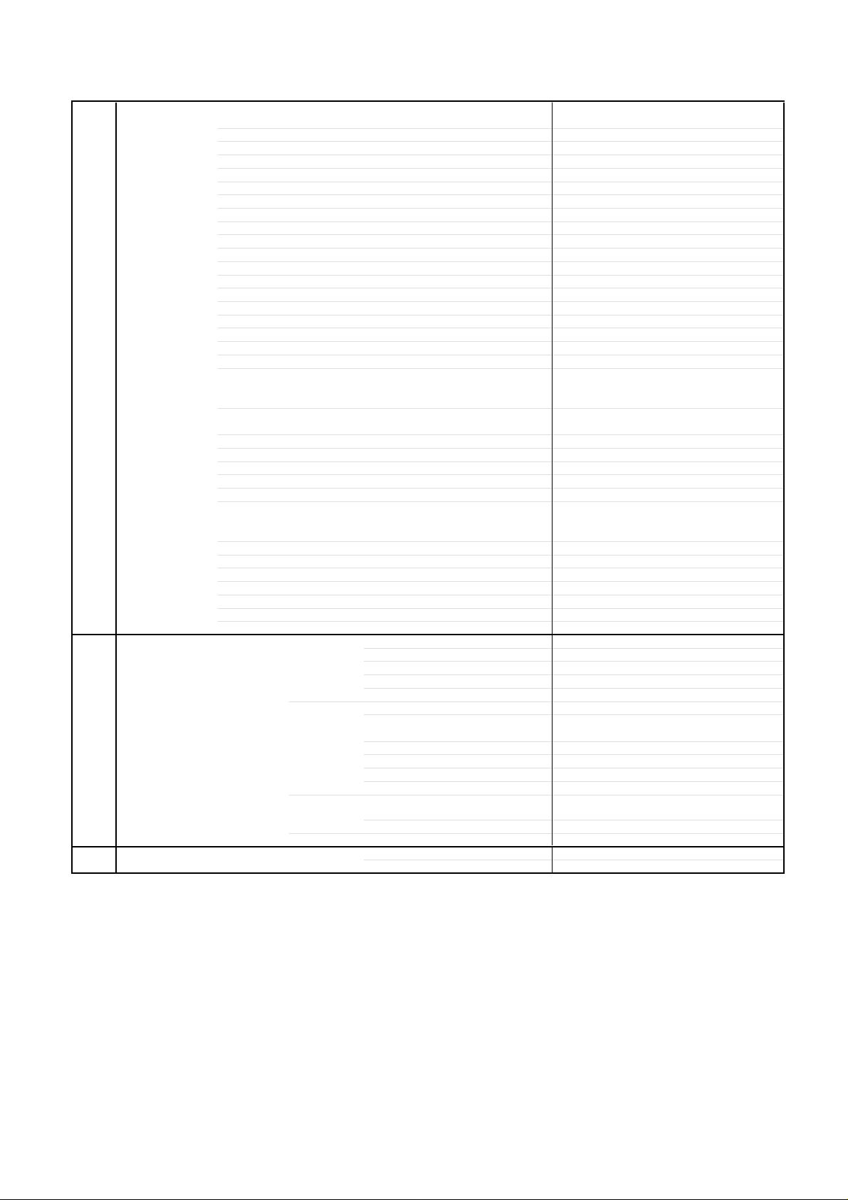
DISASSEMBLY INSTRUCTIONS
1. REMOVAL OF MECHANICAL PARTS
AND P.C. BOARDS
1-1: BACK CABINET (Refer to Fig. 1-1)
1.
Remove the 6 screws 1.
2.
Remove the 2 screws 2 which are used for holding the
Back Cabinet.
3.
Remove the AC cord from the AC cord hook 3.
4.
Remove the Back Cabinet in the direction of arrow.
Front Cabinet
1
1
1
1
1
2
2
1-2: CRT PCB (Refer to Fig. 1-2)
CAUTION: BEFORE REMOVING THE ANODE CAP,
DISCHARGE ELECTRICITY BECAUSE IT
CONTAINS HIGH VOLTAGE.
BEFORE ATTEMPTING TO REMOVE OR
REPAIR ANY PCB, UNPLUG THE POWER
CORD FROM THE AC SOURCE.
1.
Remove the Anode Cap.
(Refer to REMOVAL OF ANODE CAP)
2.
Disconnect the following connectors:
(CP801 and CP850B).
3.
Remove the CRT PCB in the direction of arrow.
3
1
Back Cabinet
Fig. 1-1
1-3: TV/DVD BLOCK (Refer to Fig. 1-3)
1.
Remove the 2 screws 1.
2.
Disconnect the following connectors:
(CP102, CP303, CP401 and CP502).
3.
Remove the TV/DVD Block in the direction of arrow.
1
Front Cabinet
TV/DVD Block
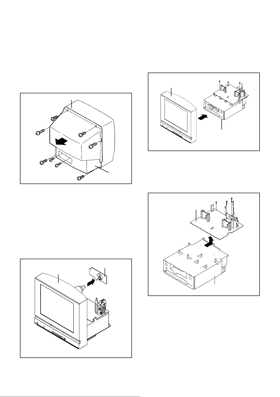
1-4: MAIN PCB (Refer to Fig. 1-4)
1.
Remove the 2 screws 1.
2.
Remove the 3 screws 2.
3.
Disconnect the following connectors:
(CP810B, CP820B and CP811).
4.
Remove the Main PCB in the direction of arrow.
2
2
1
Main PCB
2
1
1
Fig. 1-3
Front Cabinet
CRT PCB
DVD Block
Fig. 1-4
Fig. 1-2
B1-1
Page 15
DISASSEMBLY INSTRUCTIONS
1-5: FRONT TRAY PLATE/TOP SHIELD
(Refer to Fig. 1-5)
1.
Remove the Front Tray Plate in the direction of arrow (A).
2.
Remove the 9 screws 1.
3.
Remove the Top Shield in the direction of arrow (B).
1
1
1
1
1
1
(B)
Front Tray Plate
(A)
1
1
Top Shield
DVD Block
1
Fig. 1-5
3
3
CD Deck
3
3
(C)
4
2
4
4
(B)
2
(A)
Syscon PCB
Angle Deck
AV PCB
1
1
1
4
2
(D)
2
1-6: AV PCB/SYSCON PCB/CD DECK (Refer to Fig. 1-6)
1.
Remove the 3 screws 1.
2.
Remove the AV PCB in the direction of arrow (A).
3.
Remove the 4 screws 2.
4.
Remove the Angle Deck in the direction of arrow (B).
5.
Disconnect the following connectors:
(CP4001 and CP4002).
6.
Remove the 4 screws 3.
7.
Remove the CD Deck in the direction of arrow (C).
8.
Remove the 4 screws 4.
9.
Remove the Syscon PCB in the direction of arrow (D).
Bottom Plate
Fig. 1-6
B1-2
Page 16
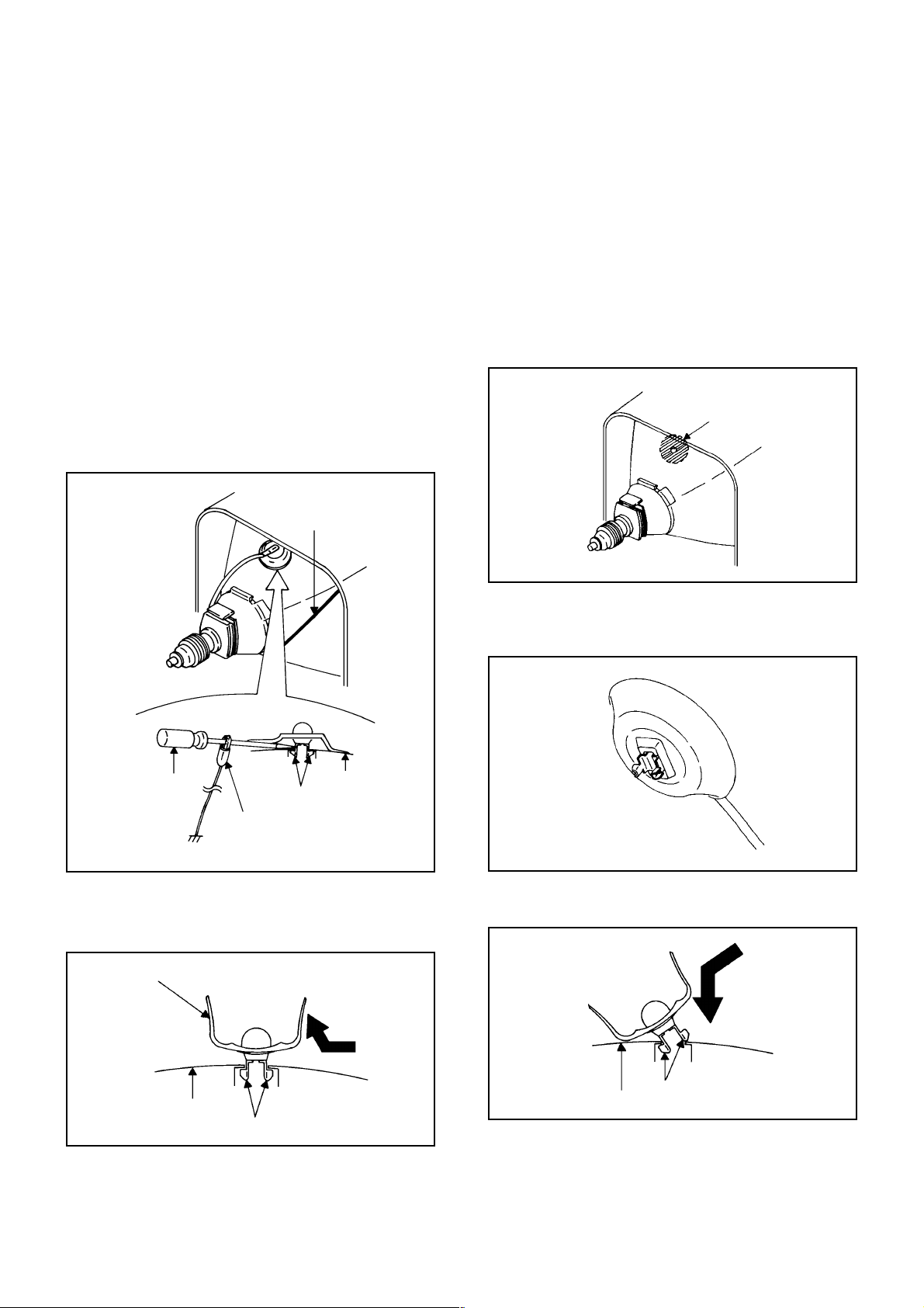
DISASSEMBLY INSTRUCTIONS
2. REMOVAL OF ANODE CAP
Read the following NOTED items before starting work.
After turning the power off there might still be a potential
*
voltage that is very dangerous. When removing the
Anode Cap, make sure to discharge the Anode Cap's
potential voltage.
*
Do not use pliers to loosen or tighten the Anode Cap
terminal, this may cause the spring to be damaged.
REMOVAL
1. Follow the steps as follows to discharge the Anode Cap.
(Refer to Fig. 2-1.)
Connect one end of an Alligator Clip to the metal part of a
flat-blade screwdriver and the other end to ground.
While holding the plastic part of the insulated Screwdriver,
touch the support of the Anode with the tip of the
Screwdriver.
A cracking noise will be heard as the voltage is discharged.
GND on the CRT
3. After one side is removed, pull in the opposite direction
to remove the other.
NOTE
Take care not to damage the Rubber Cap.
INSTALLATION
1. Clean the spot where the cap was located with a small
amount of alcohol. (Refer to Fig. 2-3.)
NOTE
Confirm that there is no dirt, dust, etc. at the spot where
the cap was located.
Location of Anode Cap
Fig. 2-3
Screwdriver
Alligator Clip
GND on the CRT
Flip up the sides of the Rubber Cap in the direction of
2.
the arrow and remove one side of the support.
(Refer to Fig. 2-2.)
Rubber Cap
Support
CRT
Fig. 2-1
2.3.Arrange the wire of the Anode Cap and make sure the
wire is not twisted.
Turn over the Rubber Cap. (Refer to Fig. 2-4.)
Fig. 2-4
4. Insert one end of the Anode Support into the anode
button, then the other as shown in Fig. 2-5.
CRT
Support
Fig. 2-2
Support
CRT
5.6.Confirm that the Support is securely connected.
Put on the Rubber Cap without moving any parts.
B2-1
Fig. 2-5
Page 17
DISASSEMBLY INSTRUCTIONS
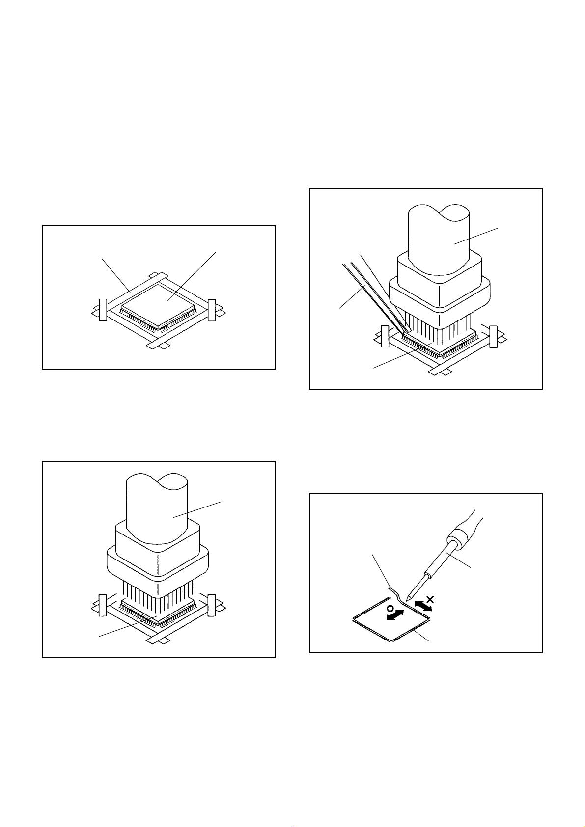
3.
REMOVAL AND INSTALLATION OF
FLAT PACKAGE IC
REMOVAL
Put the Masking Tape (cotton tape) around the Flat
1.
Package IC to protect other parts from any damage.
(Refer to Fig. 3-1.)
NOTE
Masking is carried out on all the parts located within
10 mm distance from IC leads.
When IC starts moving back and forth easily after
3.
desoldering completely, pickup the corner of the IC using
a tweezers and remove the IC by moving with the IC
desoldering machine. (Refer to Fig. 3-3.)
NOTE
Some ICs on the PCB are affixed with glue, so be
careful not to break or damage the foil of each IC
leads or solder lands under the IC when removing it.
Blower type IC
desoldering
machine
Masking Tape
(Cotton Tape)
Heat the IC leads using a blower type IC desoldering
2.
IC
machine. (Refer to Fig. 3-2.)
NOTE
Do not add the rotating and the back and forth
directions force on the IC, until IC can move back and
forth easily after desoldering the IC leads completely.
Blower type IC
desoldering machine
Fig. 3-1
Tweezers
IC
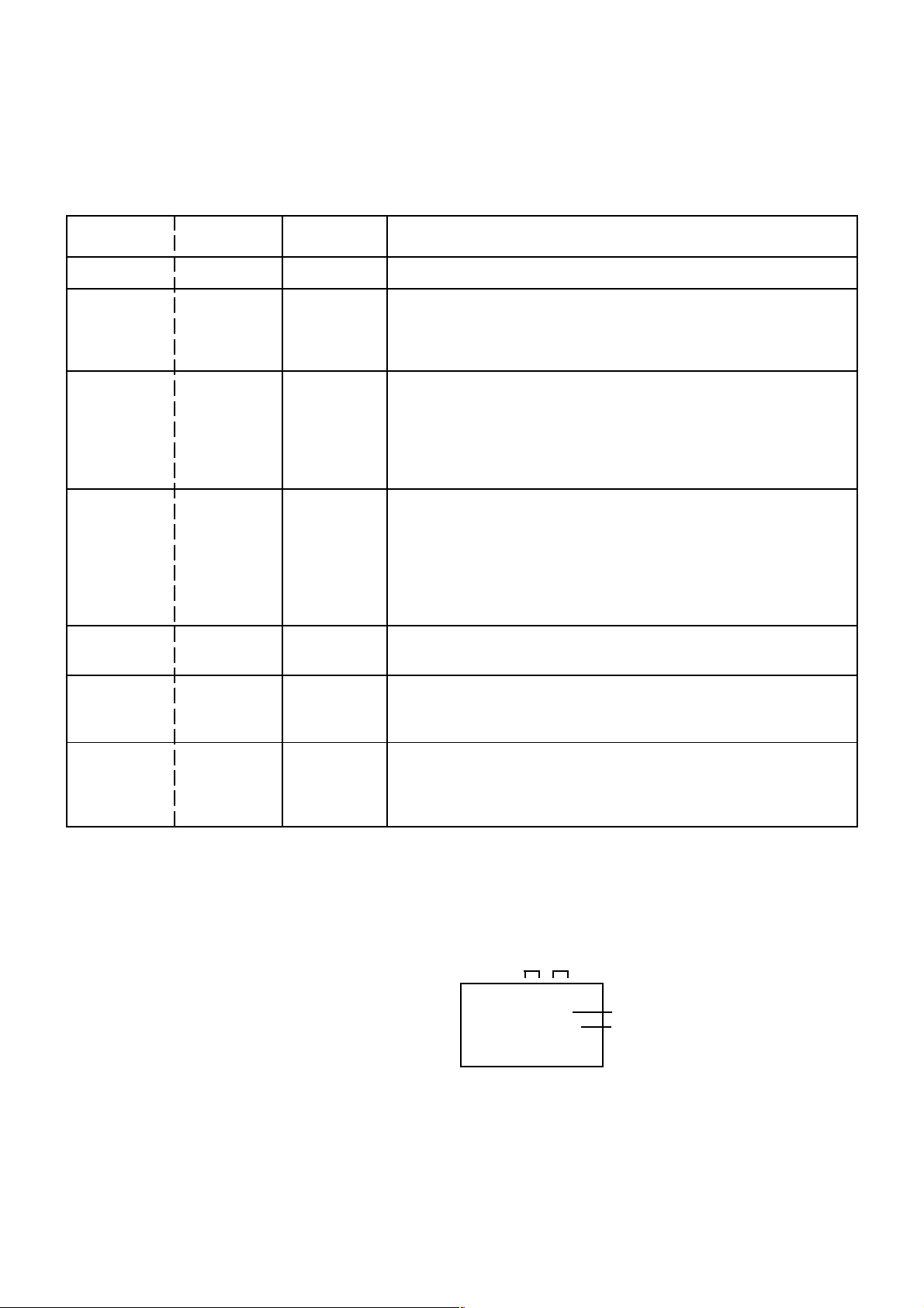
Peel off the Masking Tape.4.
Absorb the solder left on the pattern using the Braided
5.
Shield Wire. (Refer to Fig. 3-4.)
NOTE
Do not move the Braided Shield Wire in the vertical
direction towards the IC pattern.
Fig. 3-3
Braided Shield Wire
Soldering Iron
IC
Fig. 3-2
IC pattern
Fig. 3-4
B3-1
Page 18
DISASSEMBLY INSTRUCTIONS
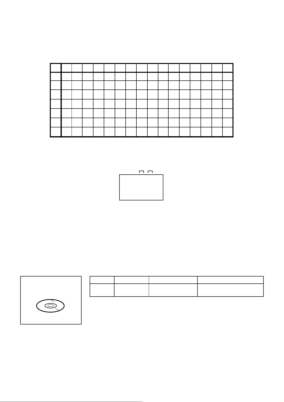
INSTALLATION
Take care of the polarity of new IC and then install the
1.
new IC fitting on the printed circuit pattern. Then solder
each lead on the diagonal positions of IC temporarily.
(Refer to Fig. 3-5.)
Soldering Iron
Solder temporarily
Supply the solder from the upper position of IC leads
2.
Solder temporarily
sliding to the lower position of the IC leads.
(Refer to Fig. 3-6.)
Fig. 3-5
When bridge-soldering between terminals and/or the
4.
soldering amount are not enough, resolder using a Thintip Soldering Iron. (Refer to Fig. 3-8.)
Thin-tip Soldering Iron
IC
Fig. 3-8
Finally, confirm the soldering status on four sides of the
5.
IC using a magnifying glass.
Confirm that no abnormality is found on the soldering
position and installation position of the parts around the
IC. If some abnormality is found, correct by resoldering.
NOTE
When the IC leads are bent during soldering and/or
repairing, do not repair the bending of leads. If the
bending of leads are repaired, the pattern may be
damaged. So, be always sure to replace the IC in this
case.
Soldering IronSolder
IC
Absorb the solder left on the lead using the Braided
3.
Supply soldering
from upper position
to lower position
Shield Wire. (Refer to Fig. 3-7.)
NOTE
Do not absorb the solder to excess.
Soldering Iron
IC
Braided Shield Wire
Fig. 3-6
Fig. 3-7
B3-2
Page 19
SERVICE MODE LIST
This unit provided with the following SERVICE MODES so you can repair, examine and adjust easily.
To enter to the SERVICE MODE function, press and hold both buttons simultaneously on the main unit and on the remote
control for more than a standard time (second).
Set Key
VOL. (-) MIN
VOL. (-) MIN 1
VOL. (-) MIN 3
VOL. (-) MIN 6
VOL. (-) MIN 8
Standard Time
(seconds)
0
1
1
1
1
1
Releasing of V-CHIP PASSWORD.
Initialization of the factory on TV.
NOTE:
Initialization of the factory on DVD.
NOTE: Do not use this for the normal servicing.
POWER ON total hours and PLAY/REC total hours are displayed on
the screen.
Refer to the "PREVENTIVE CHECKS AND SERVICE INTERVALS"
(CONFIRMATION OF HOURS USED).
Can be checked of the INITIAL DATA of MEMORY IC.
Refer to the "WHEN REPLACING EEPROM (MEMORY) IC".
Writing of EEPROM initial data.
NOTE: Do not use this for the normal servicing.
Do not use this for the normal servicing.
If you set a factory initialization, the memories are reset such as
the channel setting, and the POWER ON total hours.
The function will only work without the setting of DVD disc at
DVD mode.
While pressing the Remocon Key for more than the Standard
Time, press the Set Key simultaneously.
OperationsRemocon Key
Display of the Adjustment MENU on the screen.
VOL. (-) MIN 9
STOP 7 3
1
Refer to the "ELECTRICAL ADJUSTMENT" (On-Screen Display
Adjustment).
Releasing of PARENTAL LOCK.
Refer to the “PARENTAL CONTROL - RATING LEVEL”.
NOTE:
The function will only work without the setting of DVD disc at
DVD mode.
CONFIRMATION OF HOURS USED
POWER ON total hours can be checked on the screen. Total hours are displayed in 16 system of notation.
NOTE: If you set a factory initialization, the total hours is reset to "0".
1.
Set the VOLUME to minimum.
2.
Press both VOL. DOWN button on the set and Channel
button (6) on the remote control for more than 1 second.
3.
After the confirmation of using hours, turn off the power.
ADDRESS DATA
INIT 00 F9
CRT ON 0010
FIG. 1
Initial setting content of MEMORY IC.
POWER ON total hours.
= (16 x 16 x 16 x thousands digit value)
+ (16 x 16 x hundreds digit value)
+ (16 x tens digit value)
+ (ones digit value)
C-1
Page 20
WHEN REPLACING EEPROM (MEMORY) IC
If a service repair is undertaken where it has been required to change the MEMORY IC, the following steps should be taken to
ensure correct data settings while making reference to TABLE 1.
Note: No need setting for the position of the mark @ due to the adjustment value.
INI
+0 +1 +2 +3 +4 +5 +6 +7 +8 +9 +A +B +C +D +E +F
00 D9 3F 3F 40 61 63
F9 43 25 01 F1 23 27 F7 81 CD
64 67 69 2A 6B 6C 6D 6E 6F10 26 70 71 52 72 53 73
54 55 75 75 56 56 76 76 5720 74 57 77 77 58 58 78
78 59 79 79 5A 5A 7A 7A 5B30 59 5B 7B 7B 5C 5C 7C
7C 5D 7D 7D 5E 5E 7E 7E 5F40 5D 5F 5F 7F 7F @ @
@@@@@@@@@50 @ @ @ @ @ @ @
@@@@@@@@@60 @ @ 10 --- --- --- ---
Table 1
1.
Enter DATA SET mode by setting VOLUME to minimum.
2.
Press both VOL. DOWN button on the set and Channel button (6) on the remote control for more than 1 second.
ADDRESS and DATA should appear as FIG 1.
ADDRESS DATA
INIT 00 F9
CRT ON 0010
FIG. 1
3.
ADDRESS is now selected and should "blink". Using the VOL. UP/DOWN button on the remote, step through the
ADDRESS until required ADDRESS to be changed is reached.
4.
Press ENTER to select DATA. When DATA is selected, it will "blink".
5.
Again, step through the DATA using VOL. UP/DOWN button until required DATA value has been selected.
6.
Pressing ENTER will take you back to ADDRESS for further selection if necessary.
7.
Repeat steps 3 to 6 until all data has been checked.
8.
When satisfied correct DATA has been entered, turn POWER off (return to STANDBY MODE) to finish DATA input.
The unit will now have the correct DATA for the new MEMORY IC.
SERVICING FIXTURES AND TOOLS
JG175A
DVD Test Disc
(A-BEX TDV-540)
Ref. No.
JG175A
Part No.
APJG175A00
Parts Name
DVD Test Disc
(A-BEX TDV-540)
Tint adjustment of DVD mode
Remarks
C-2
Page 21
ELECTRICAL ADJUSTMENTS
1.
BEFORE MAKING ELECTRICAL
ADJUSTMENTS
Read and perform these adjustments when repairing the
circuits or replacing electrical parts or PCB assemblies.
CAUTION
•
Use an isolation transformer when performing any
service on this chassis.
•
Before removing the anode cap, discharge electricity
because it contains high voltage.
•
When removing a PCB or related component, after
unfastening or changing a wire, be sure to put the wire
back in its original position.
•
When you exchange IC and Transistor for a heat sink,
apply the silicon grease on the contact section of the
heat sink. Before applying new silicon grease, remove all
the old silicon grease. (Old grease may cause damages
to the IC and Transistor).
Prepare the following measurement tools for electrical
adjustments.
1. Oscilloscope
2. Digital Voltmeter
3. AC Voltmeter
4. Pattern Generator
5. Multi-Sound Signal Generator
NO.
FUNCTION
01
R CUT OFF
02
G CUT OFF
03
B CUT OFF
04
G DRIVE
05
B DRIVE
06
BRIGHTNESS(CENT.)
07
BRIGHTNESS(MAX)
08
BRIGHTNESS(MIN)
09
COLOR(CENT.)
10
COLOR(MAX)
11
COLOR(MIN)
12
TINT
13
SUB CONTRAST
14
CONTRAST(CENT.)
15
CONTRAST(MAX)
16
CONTRAST(MIN)
17
SHARPNESS
18
RGB CONTRAST
19
H POSITION
20
V POSITION
21
V SIZE
22
V LINEARITY
23
V S CORRECTION
24
EW PARABOLA CORR.
25
EW TRAPEZIUM CORR.
26
H SIZE
27
V EHT
28
H EHT
29
RF AGC
30
V CENTERING
31
CORNER CORR. TOP
32
CORNER CORR. BTM
33
OSD H
34
FM LEVEL
35
TEST PWM
36
TEST TONE CONTROL
FUNCTION
NO.
BRI. AV(CENT.)
37
BRI. AV(MAX)
38
BRI. AV(MIN)
39
COL. AV(CENT.)
40
COL. AV(MAX)
41
COL. AV(MIN)
42
TINT AV
43
SUB CONTRAST AV
44
CONT. AV(CENT.)
45
CONT. AV(MAX)
46
CONT. AV(MIN)
47
SHARPNESS AV
48
BRI. DVD(CENT.)
49
BRI. DVD(MAX)
50
BRI. DVD(MIN)
51
COL. DVD(CENT.)
52
COL. DVD(MAX)
53
COL. DVD(MIN)
54
TINT DVD
55
SUB CONTRAST DVD
56
CONT. DVD(CENT.)
57
CONT. DVD(MAX)
58
CONT. DVD(MIN)
59
SHARPNESS DVD
60
BRI. GAME(CENT.)
61
BRI. GAME(MAX)
62
BRI. GAME(MIN)
63
CONT. GAME(CENT.)
64
CONT. GAME(MAX)
65
CONT. GAME(MIN)
66
TUNING V MUTE
67
POWER ON V MUTE
68
INPUT LEVEL
69
SEPARATION L
70
SEPARATION H
71
CUT OFF
72
Fig. 1-2
On-Screen Display Adjustment
In the condition of NO indication on the screen.
1.
Press the VOL. DOWN button on the set and the
Channel button (9) on the remote control for more than
1 second to appear the adjustment mode on the screen
as shown in Fig. 1-1.
Function
Step No.
Use the Channel UP/DOWN button or Channel button
2.
01 RCUT
3E
(1-0) on the remote control to select the options shown
in Fig. 1-2.
Press the MENU button on the remote control to end
3.
the adjustments.
Fig. 1-1
2. BASIC ADJUSTMENTS
2-1: CONSTANT VOLTAGE
1.
Set condition is AV MODE without signal.
2.
Using the remote control, set the brightness and contrast
to normal position.
3.
Connect the digital voltmeter to TP401.
4.
Adjust the VR502 until the digital voltmeter is 111 ± 0.5V.
2-2: RF AGC
1.
Receive the VHF HIGH (63dB).
2.
Place the set with Aging Test for more than 15 minutes.
3.
Connect the digital voltmeter between the pin 5 of
CP101 and the pin 1 of CP101.
4.
Activate the adjustment mode display of Fig. 1-1 and
press the channel button (29) on the remote control to
select "AGC".
5.
Press the RIGHT/LEFT button on the remote control
until the digital voltmeter is 2.7 ± 0.05V.
2-3: FOCUS
1.
Receive the monoscope pattern.
2.
Turn the Focus Volume fully counterclockwise once.
3.
Adjust the Focus Volume until picture is distinct.
2-4: CUT OFF
1.
Adjust the unit to the following settings.
R CUT=7F, G CUT=7F, B CUT=7F, G DRV=3F,
B DRV=3F
2.
Place the set with Aging Test for more than 15 minutes.
3.
Set condition is AV MODE without signal.
4.
Using the remote control, set the brightness and contrast
to normal position.
5.
Activate the adjustment mode display of Fig. 1-1 and
press the channel button (72) on the remote control to
select "CUT OFF".
6.
Adjust the Screen Volume until a dim raster is obtained.
D-1
Page 22

ELECTRICAL ADJUSTMENTS
2-5: WHITE BALANCE
NOTE: Adjust after performing CUT OFF adjustment.
1.
Place the set with Aging Test for more than 15 minutes.
2.
Receive the gray scale pattern from the Pattern
Generator.
3.
Using the remote control, set the brightness and
contrast to normal position.
4.
Activate the adjustment mode display of Fig. 1-1 and
press the channel button (04) on the remote control to
select "G DRV".
5.
Press the CH. UP/DOWN button on the remote control
to select the "R CUT", "G CUT", "B CUT", "G DRV" or
"B DRV".
6.
Adjust the RIGHT/LEFT button on the remote control to
whiten the R CUT, G CUT, B CUT, G DRV, and B DRV
at each step tone sections equally.
7.
Perform the above adjustments 5 and 6 until the white
color is looked like a white.
2-6: HORIZONTAL POSITION
1.
Receive the monoscope pattern.
2.
Using the remote control, set the brightness and
contrast to normal position.
3.
Activate the adjustment mode display of Fig. 1-1 and
press the channel button (19) on the remote control to
select "HPOSI".
4.
Press the RIGHT/LEFT button on the remote control
until the SHIFT quantity of the OVER SCAN on right
and left becomes minimum.
2-7: HORIZONTAL SIZE
1.
Receive the monoscope pattern.
2.
Using the remote control, set the brightness and
contrast to normal position.
3.
Activate the adjustment mode display of Fig. 1-1 and
press the channel button (26) on the remote control to
select "WIDS".
4.
Press the RIGHT/LEFT button on the remote control
until the SHIFT quantity of the OVER SCAN on right
and left becomes 10 ± 2%.
2-8: VERTICAL SHIFT
1.
Receive the monoscope pattern.
2.
Using the remote control, set the brightness and
contrast to normal position.
3.
Activate the adjustment mode display of Fig. 1-1 and
press the channel button (20) on the remote control to
select "VPOSI".
4.
Press the RIGHT/LEFT button on the remote control
until the horizontal line becomes fit to the notch of the
shadow mask.
2-9: VERTICAL SIZE
1.
Receive the monoscope pattern.
2.
Using the remote control, set the brightness and
contrast to normal position.
3.
Activate the adjustment mode display of Fig. 1-1 and
press the channel button (21) on the remote control to
select "VSIZE".
4.
Press the RIGHT/LEFT button on the remote control
until the Up/Down OVER SCAN Quantity becomes
equal to the Right/Left OVER SCAN Quantity.
5.
Receive a broadcast and check if the picture is normal.
2-10: VERTICAL LINEARITY
NOTE:
1.
2.
3.
4.
2-11: PARABOLA CORR
1.
2.
3.
4.
2-12: TRAPEZIUM
1.
2.
3.
4.
2-13: CORNER CORR TOP
1.
2.
3.
4.
2-14: CORNER CORR BOTTOM
1.
2.
3.
4.
Adjust after performing adjustments in section 2-9.
After the adjustment of Vertical Linearity, reconfirm
the Vertical Shift and Vertical Size adjustments.
Receive the monoscope pattern.
Using the remote control, set the brightness and
contrast to normal position.
Activate the adjustment mode display of Fig. 1-1 and
press the channel button (22) on the remote control to
select "VLIN".
Press the RIGHT/LEFT button on the remote control
until the SHIFT quantity of the OVER SCAN on upside
and downside becomes minimum.
Receive the rainbow pattern from the Pattern Generator.
Using the remote control, set the brightness and
contrast to normal position.
Activate the adjustment mode display of Fig. 1-1 and
press the channel button (24) on the remote control to
select "DPCS".
Press the RIGHT/LEFT button on the remote control
until the right and left vertical lines are straight.
Receive the rainbow pattern from the Pattern Generator.
Using the remote control, set the brightness and
contrast to normal position.
Activate the adjustment mode display of Fig. 1-1 and
press the channel button (25) on the remote control to
select "KEYS".
Press the RIGHT/LEFT button on the remote control
until the both vertical lines of the screen become
parallel.
Receive the rainbow pattern from the Pattern Generator.
Using the remote control, set the brightness and
contrast to normal position.
Activate the adjustment mode display of Fig. 1-1 and
press the channel button (31) on the remote control to
select "CNRT".
Press the RIGHT/LEFT button on the remote control
until the upper section of the both ends vertical lines are
straight.
Receive the rainbow pattern from the Pattern Generator.
Using the remote control, set the brightness and
contrast to normal position.
Activate the adjustment mode display of Fig. 1-1 and
press the channel button (32) on the remote control to
select "CNRB".
Press the RIGHT/LEFT button on the remote control
until the bottom section of the both ends vertical lines
are straight.
D-2
Page 23

ELECTRICAL ADJUSTMENTS
Please do the method (1) or method (2) adjustment.
Method (1)
1.
Set the multi-sound signal generator for each different
L-ch and R-ch frequency (Ex. L-ch=2KHz, R-ch=400Hz)
and receive the RF signal.
2.
Connect the oscilloscope to the Audio Out Jack.
3.
Press the AUDIO button on the remote control to set to
the stereo mode.
4.
Activate the adjustment mode display of Fig. 1-1 and
press the channel button (70) on the remote control to
select “SEPAL”.
5.
Press the RIGHT/LEFT button on the remote control to
adjust it until the audio output wave becomes a fine
sine wave.
6.
Press the CH UP button 1 time to set to "SEPAH"
mode.
7.
Press the RIGHT/LEFT button on the remote control to
adjust it until the audio output wave becomes a fine
sine wave.
Method (2)
1.
Set the multi-sound signal generator L-ch=1KHz, R-ch
=Non input and receive the RF signal.
2.
Connect the oscilloscope to the Audio Out Jack (R-ch).
3.
Press the AUDIO button on the remote control to set to
the stereo mode.
4.
Activate the adjustment mode display of Fig. 1-1 and
press the channel button (70) on the remote control to
select “SEPAL”.
5.
Press the RIGHT/LEFT button on the remote control to
adjust it until the R-ch output becomes minimum.
6.
Press the CH UP button 1 time to set to "SEPAH" mode.
7.
Press the RIGHT/LEFT button on the remote control to
adjust it until the R-ch output becomes minimum.
8.
Set the multi-sound signal generator L-ch=Non input,
R-ch=1KHz and receive the RF signal.
9.
Connect the oscilloscope to the Audio Out Jack (L-ch).
Then perform the above adjustments 3~7.
2-16: OSD HORIZONTAL
Activate the adjustment mode display of Fig. 1-1 and
1.
press the channel button (33) on the remote control to
select "OSD".
Press the RIGHT/LEFT button on the remote control
2.
until the difference of A and B becomes minimum.
(Refer to Fig. 2-1)
2-17: LEVEL2-15: SEPARATION
1.
Receive the VHF HIGH (70dB).
2.
Connect the AC voltmeter to TP901.
3.
Activate the adjustment mode display of Fig. 1-1 and
press the channel button (69) on the remote control to
select "LVL".
4.
Press the RIGHT/LEFT button on the remote control
until the AC voltmeter is 75 ± 2mV.
2-18: SUB BRIGHT CENTER
1.
Receive the monoscope pattern. (RF Input)
2.
Using the remote control, set the brightness and
contrast to normal position.
3.
Activate the adjustment mode display of Fig. 1-1 and
press the channel button (06) on the remote control to
select "BRTC".
4.
Press the RIGHT/LEFT button on the remote control
until the white 15% is starting to be visible
5.
Receive the monoscope pattern. (Audio Video Input)
6.
Press the INPUT SELECT button on the remote control
to set to the AV mode.
7.
Using the remote control, set the brightness and
contrast to normal position.
8.
Activate the adjustment mode display of Fig. 1-1 and
press the channel button (37) on the remote control to
select "BRTCA".
9.
Press the RIGHT/LEFT button on the remote control
until the white 15% is starting to be visible
10.
Press the TV/DVD button on the remote control to set to
the DVD mode.
11.
Activate the adjustment mode display of Fig. 1-1 and
press the channel button (49) on the remote control to
select "BRTCD".
12.
Press the RIGHT/LEFT button on the remote control to
set the same step numbers as the AV.
13.
Press the GAME button on the remote control to set to
the GAME mode.
14.
Activate the adjustment mode display of Fig. 1-1 and
press the channel button (61) on the remote control to
select "BRTCG".
15.
Press the RIGHT/LEFT button on the remote control to
decrease the step numbers by 16 steps to the AV.
A
33 OSD
15
B
Fig. 2-1
D-3
Page 24

ELECTRICAL ADJUSTMENTS
2-19: SUB TINT CENTER
1.
Receive the color bar pattern. (RF Input)
2.
Using the remote control, set the brightness, contrast,
color and tint to normal position.
3.
Connect the oscilloscope to TP803.
4.
Activate the adjustment mode display of Fig. 1-1 and
press the channel button (12) on the remote control to
select "TNTC".
5.
Press the RIGHT/LEFT button on the remote control
until the section "A" becomes a straight line.
(Refer to Fig. 2-2)
6.
Receive the color bar pattern. (Audio Video Input)
7.
Press the INPUT SELECT button on the remote
control to set to the AV mode.
8.
Using the remote control, set the brightness, contrast,
color and tint to normal position.
9.
Activate the adjustment mode display of Fig. 1-1 and
press the channel button (43) on the remote control to
select "TNTCA".
10.
Press the RIGHT/LEFT button on the remote control
until the section "A" becomes a straight line.
(Refer to Fig. 2-2)
11.
Press the TV/DVD button on the remote control to set
to the DVD mode.
12.
Playback the Title2 (color bar pattern) of JG175A.
13.
Activate the adjustment mode display of Fig. 1-1 and
press the channel button (55) on the remote control to
select "TNTCD".
14.
Press the RIGHT/LEFT button on the remote control
until the section "B" becomes a straight line.
(Refer to Fig. 2-3)
2-20: SUB COLOR CENTER
1.
Receive the color bar pattern. (RF Input)
2.
Using the remote control, set the brightness, contrast,
color and tint to normal position.
3.
Connect the oscilloscop to TP801.
4.
Activate the adjustment mode display of Fig. 1-1 and
press the channel button (09) on the remote control to
select "COLC".
5.
Adjust the VOLTS RANGE VARIABLE knob of the
oscilloscope until the range between white 100% and
0% is set to 4 scales on the screen of the oscilloscope.
6.
Press the RIGHT/LEFT button on the remote control
until the red color level is adjusted to 120 ± 5% of the
white level. (Refer to Fig. 2-4)
7.
Receive the color bar pattern. (Audio Video Input)
8.
Press the INPUT SELECT button on the remote control
to set to the AV mode.
9.
Using the remote control, set the brightness, contrast,
color and tint to normal position.
10.
Activate the adjustment mode display of Fig. 1-1 and
press the channel button (40) on the remote control to
select "COLCA".
11.
Adjust the VOLTS RANGE VARIABLE knob of the
oscilloscope until the range between white 100% and
0% is set to 4 scales on the screen of the oscilloscope.
12.
Press the RIGHT/LEFT button on the remote control
until the red color level is adjusted to 120 ± 5% of the
white level. (Refer to Fig. 2-4)
13.
Press the TV/DVD button on the remote control to set
to the DVD mode.
14.
Activate the adjustment mode display of Fig. 1-1 and
press the channel button (52) on the remote control to
select "COLCD".
15.
Press the RIGHT/LEFT button on the remote control to
increase the step numbers by 3 steps to the AV.
"B"
"A"
Fig. 2-2
Fig. 2-3
White 0%
White 100%
Red Level
0%
100%
Fig. 2-4
D-4
Page 25

ELECTRICAL ADJUSTMENTS
2-21: SUB CONTRAST MAX
Activate the adjustment mode display of Fig. 1-1 and
1.
press the channel button (15) on the remote control to
select "CNTX".
Press the RIGHT/LEFT button on the remote control
2.
until the contrast step No. becomes "61"
Receive a broadcast and check if the picture is normal.
3.
Press the INPUT SELECT button on the remote
4.
control to set to the AV mode.
Activate the adjustment mode display of Fig. 1-1 and
5.
press the channel button (46) on the remote control to
select "CNTXA".
Press the RIGHT/LEFT button on the remote control
6.
until the contrast step No. becomes "65"
Receive a broadcast and check if the picture is normal.
7.
Press the TV/DVD button on the remote control to set
8.
to the DVD mode.
Activate the adjustment mode display of Fig. 1-1 and
9.
press the channel button (58) on the remote control to
select "CNTXD".
Press the RIGHT/LEFT button on the remote control to
10.
set the same step numbers as the AV mode.
Press the GAME button on the remote control to set to
11.
the GAME mode.
Activate the adjustment mode display of Fig. 1-1 and
12.
press the channel button (65) on the remote control to
select "CNTXG".
Press the RIGHT/LEFT button on the remote control to
13.
set the same step numbers as the AV mode.
2-22: Confirmation of Fixed Value (Step No.)
Please check if the fixed values of the each adjustment
items are set correctly referring below.
NO.
FUNCTION
07
BRIGHTNESS(MAX)
08
BRIGHTNESS(MIN)
10
COLOR(MAX)
11
COLOR(MIN)
13
SUB CONTRAST
14
CONTRAST(CENT.)
16
CONTRAST(MIN)
17
SHARPNESS
18
RGB CONTRAST
23
V S CORRECTION
27
V EHT
28
H EHT
30
V CENTERING
34
FM LEVEL
35
TEST PWM
36
TEST TONE CONTROL
38
BRI. AV(MAX)
39
BRI. AV(MIN)
41
COL. AV(MAX)
STEP NO.
7F
00
7F
00
07
3F
10
38
21
0A
02
02
18
01
00
51
7F
00
7F
NO.
FUNCTION
42
COL. AV(MIN)
44
SUB CONTRAST AV
45
CONT. AV(CENT.)
47
CONT. AV(MIN)
48
SHARPNESS AV
50
BRI. DVD(MAX)
51
BRI. DVD(MIN)
53
COL. DVD(MAX)
54
COL. DVD(MIN)
56
SUB CONTRAST DVD
57
CONT. DVD(CENT.)
59
CONT. DVD(MIN)
60
SHARPNESS DVD
62
BRI. GAME(MAX)
63
BRI. GAME(MIN)
64
CONT. GAME(CENT.)
66
CONT. GAME(MIN)
67
TUNING V MUTE
68
POWER ON V MUTE
STEP NO.
00
07
3F
10
38
7F
00
7F
00
07
3F
10
2D
7F
00
3F
10
08
90
D-5
Page 26

ELECTRICAL ADJUSTMENTS
3.
PURITY AND CONVERGENCE
ADJUSTMENTS
NOTE
1.
Turn the unit on and let it warm up for at least 30
minutes before performing the following adjustments.
2.
Place the CRT surface facing east or west to reduce the
terrestrial magnetism.
3.
Turn ON the unit and demagnetize with a Degauss Coil.
3-1: STATIC CONVERGENCE (ROUGH ADJUSTMENT)
1.
Tighten the screw for the magnet. Refer to the adjusted
CRT for the position. (Refer to Fig. 3-1)
If the deflection yoke and magnet are in one body,
untighten the screw for the body.
2.
Receive the green raster pattern from the color bar
generator.
3.
Slide the deflection yoke until it touches the funnel
side of the CRT.
4.
Adjust center of screen to green, with red and blue on the
sides, using the pair of purity magnets.
5.
Switch the color bar generator from the green raster
pattern to the crosshatch pattern.
6.
Combine red and blue of the 3 color crosshatch pattern
on the center of the screen by adjusting the pair of
4 pole magnets.
7.
Combine red/blue (magenta) and green by adjusting the
pair of 6 pole magnets.
8.
Adjust the crosshatch pattern to change to white
by repeating steps 6 and 7.
3-2: PURITY
NOTE
Adjust after performing adjustments in section 3-1.
3-3: STATIC CONVERGENCE
NOTE
Adjust after performing adjustments in section 3-2.
1.
Receive the crosshatch pattern from the color bar
generator.
2.
Combine red and blue of the 3 color crosshatch pattern
on the center of the screen by adjusting the pair of
4 pole magnets.
3.
Combine red/blue (magenta) and green by adjusting the
pair of 6 pole magnets.
3-4: DYNAMIC CONVERGENCE
NOTE
Adjust after performing adjustments in section 3-3.
1.2.Adjust the differences around the screen by moving
the deflection yoke upward/downward and right/left.
(Refer to Fig. 3-2-a)
Insert three wedges between the deflection yoke and
CRT funnel to fix the deflection yoke.
(Refer to Fig. 3-2-b)
R G B
R
G
B
UPWARD/DOWNWARD SLANT RIGHT/LEFT SLANT
R
G
B
Fig. 3-2-a
R G B
1.
Receive the green raster pattern from color bar
generator.
2.
Adjust the pair of purity magnets to center the
color on the screen.
Adjust the pair of purity magnets so the color at the
ends are equally wide.
3.
Move the deflection yoke backward (to neck side)
slowly, and stop it at the position when the whole
screen is green.
4.
Confirm red and blue colors.
5.
Adjust the slant of the deflection yoke while watching the
screen, then tighten the fixing screw.
DEFLECTION YOKE
DEFLECTION YOKE SCREW
MAGNET SCREW
PURITY MAGNETS
6 POLE MAGNETS
4 POLE MAGNETS
Fig. 3-1
WEDGE
WEDGE
WEDGE
WEDGE POSITION
Fig. 3-2-b
D-6
Page 27

ELECTRICAL ADJUSTMENTS
4. ELECTRICAL ADJUSTMENT PARTS LOCATION GUIDE (WIRING CONNECTION)
CP810B
CP811
TOP SHIELD
CD502
CP502
CP820B
CP506
CP507
L503
VR502
CRT PCB
TP801
CP850B
TP803
CD850
CD820
CD810
CP403
CP401
CRT
J801
CD401
FB401
CRT
CP803B
TP401
CP803A
CP807
CP801
CD803
R449
CD801
CRT
CD8001
CP8001
CP303
CD356
J7001
8004
P
C
CP8005
CP8002
AV PCB
SPEAKER
OPERATION PCB
CP101
CP8003
SPEAKER
CD403
J7003
CP8006
J7002
TU001
TP901
CP102
CD8002
CD355
AC IN
CD501
CD811
DECK CD
CD402
TOP SHIELD
MAIN PCB
CD702
CP8501
CP8502
CP4001
CP4002
SYSCON PCB
CD4001
CD4002
CD757
D-7
Page 28

MECHANICAL EXPLODED VIEW
118
124
203
203
118
201
201
203
203
PCB110
(CRT PCB)
205
121
119
207
109
201
205
206
208
207
201
207
201
201
128
206
206
120
103
116
204
204
PCB070
(MAIN PCB)
PCB030
(OPERATION PCB)
204
204
B
101
205
204
205
206
104
A
109
208
I-1
Page 29

126
MECHANICAL EXPLODED VIEW
207
207
207
207
207
207
207
207
207
PCB010
(SYSCON PCB)
207 109
207
207
207
207
122
207
207
A
207
207
109
207
207
115
207
206
207
205
115
112
207
202
202
B
110
PCB250
(AV PCB)
I-2
Page 30

MECHANICAL REPLACEMENT PARTS LIST
Location No. TSB P/N Reference No. Description
101 BZ310446 A587080720 CABINET,FRONT ASSY
103 BZ710396 713WPA0147 GLASS,LED
104 BZ710459 761WPA0223 HOLDER,FBT
109 BZ710039 8995034000 CORD CLIP UL CO.
110 BZ710420 702WSAA026 PLATE,BOTTOM
112 BZ710398 761WSA0079 ANGLE,DECK
115 BZ710401 769WPA0018 GUIDE,CONNECTOR(FFC)
116 BZ710735 701WPJB770 CABINET,FRONT
118 BZ710259 762WPA0011 HOLDER,CRT WIRE
119 BZ310447 A587080740 CABINET,BACK ASSY
120 BZ710736 735WPBA421 BUTTON,FRAME
121 BZ710422 702WPA0823 CABINET,BACK
122 BZ710406 702WSA0075 SHIELD,TOP
124 BZ710258 741WUA0001 SPRING,EARTH
126 BZ710407 712WPB0075 PLATE,TRAY-FRONT
128 BZ710260 899HV3T000 HOLDER,ANODE WIRE
201 BZ710035 8117540A64 SCREW,TAPPING(B0) TRUSS 4x16
202 BZ710320 8117540804 SCREW,TAPPING(B0) TRUSS 4x8
203 BZ710275 8121J50B54 SCREW,TAPPING(B0) GW20 5x28
204 BZ710031 8110630A04 SCREW,TAP TITE(P) BRAZIER 3x10
205 BZ710239 8109I30A04 SCREW,TAP TITE(B) WH7 3x10
206 BZ710019 8109630802 SCREW,TAP TITE(B) BRAZIER 3x8
207 BZ710408 8109630604 SCREW,TAP TITE(B) BRAZIER 3x6
208 BZ710409 8107630B04 SCREW,TAP TITE(S) BRAZIER 3x20
--- BZ710410 792WHA0317 PACKAGE,TOP
--- BZ710411 792WHA0318 PACKAGE,BOTTOM
--- BZ710746 793WCDB394 GIFT BOX
--- BZ614471 J5870801 INSTRUCTION BOOK
J1-1
Page 31

ELECTRICAL REPLACEMENT PARTS LIST
Location No. TSB P/N Reference No. Description
RESISTORS
! R402 BZ210165 R3X18AR56J R,METAL OXIDE 0.56 OHM 2W
! R410 BZ210166 R002T4562J RC 5.6K OHM 1/4W
! R418 BZ210053 R002T22R2J RC 2.2 OHM 1/2W
! R439 BZ210151 R4X5T4273F R,METAL 27K OHM 1/4W
! R441 BZ210013 R4X5T4104F R,METAL 100K OHM 1/4W
! R442 BZ210016 R4X5T4822F R,METAL 8.2K OHM 1/4W
! R443 BZ210167 R4X5T4102F R,METAL 1K OHM 1/4W
! R444 BZ210152 R4X5T4103F R,METAL 10K OHM 1/4W
! R447 BZ210021 R65582680J R,FUSE 68 OHM 1/2W
! R448 BZ210153 R3X181102J R,METAL OXIDE 1K OHM 1W
! R449 BZ210168 R5X2CE222J R,CEMENT 2.2K OHM 7W or
! R450 BZ210169 R6358A4R7J R,FUSE 4.7 OHM 2W
R461 BZ210170 R3X18A5R6J R,METAL OXIDE 5.6 OHM 2W
! R500 BZ210001 R21202275K R,SOLID 2.7M OHM 1/2W
! R501 BZ210031 R5X2CE1R2J R,CEMENT 1.2 OHM 7W
! R505 BZ210171 R3X28B333J R,METAL OXIDE 33K OHM 3W
! R509 BZ210172 R65584010J R,FUSE 1 OHM 1/4W
! R529 BZ210084 R4X5T4272F R,METAL 2.7K OHM 1/4W or
! R542 BZ210002 R33681R15J R,METAL OHMJ 0.15OHM 1W
! R543 BZ210086 R635U4681J R,FUSE 680 OHM 1/4W
! R802 BZ210050 R3X18A123J R,METAL OXIDE 12K OHM 2W
! R805 BZ210050 R3X18A123J R,METAL OXIDE 12K OHM 2W
! R810 BZ210050 R3X18A123J R,METAL OXIDE 12K OHM 2W
BZ210266 R5W1CE222J R,CEMENT 2.2K OHM 7W
BZ210034 R412T4272F R,METAL 2.7K OHM 1/4W
CAPACITORS
C313 BZ110078 E02L03102M CE 1000 UF 25V
! C407 BZ110101 E5EZF3222M CE 2200 UF 25V
! C421 BZ110014 E5EZ04102M CE 1000 UF 35V
C423 BZ210173 P4J7F3474J CMPP 0.47 UF 250V PMS
! C424 BZ110172 C03L0R7U2K CC 680 PF 2KV R
! C426 BZ210174 P4N8FJ472H CMPP 0.0047UF 1.25KV
! C427 BZ110137 P4N8FJ822H CMPP 0.0082UF 1.25KV
! C428 BZ210175 P3N1F5473J CPP 0.047 UF 630V
! C431 BZ110103 E02LTD100M CE 10 UF 250V
! C433 BZ110020 E5EZT8220M CE 22 UF 100V
C442 BZ110057 E53FF56R8K CE 6.8 UF 50V NP
C450 BZ110182 C03L0R713K CC 0.001 UF 2KV R
! C502 BZ110009 C13HB07H3K CC 0.0022UF 2KV B
! C503 BZ110009 C13HB07H3K CC 0.0022UF 2KV B
! C504 BZ110039 E02LT1102M CE 1000 UF 10V
! C505 BZ110138 P2472B224M CMP 0.22UF 275V PHE840
! C506 BZ110138 P2472B224M CMP 0.22UF 275V PHE840
! C507 BZ110062 E51SFC821M CE 820 UF 200V
! C510 BZ110063 E5EZT5470M CE 47 UF 50V
C514 BZ110191 C03L0R7E3K CC 0.0015UF 2KV R
C517 BZ110191 C03L0R7E3K CC 0.0015UF 2KV R
C518 BZ110172 C03L0R7U2K CC 680 PF 2KV R
! C520 BZ110135 E02L02222M CE 2200 UF 16V
! C521 BZ110130 E62NFC221M CE 220 UF 200V
! C523 BZ210176 E02LF3222M CE 2200 UF 25V
! C524 BZ210177 E02LU2470M CE 47 UF 16V
C526 BZ110249 E52H02100M CE 10 UF 16V or
! C529 BZ110082 C034F0JL3M CC 0.0033UF 125V MX
! C531 BZ210178 E62FT2471M CE 470 UF 16V
! C535 BZ110023 E62DFB470M CE 47 UF 160V
! C538 BZ210179 E5EZTB4R7M CE 4.7 UF 160V
C819 BZ110141 C0HHB07H3K CC 0.0022UF 2KV B or
C7003 BZ110155 E02L02471M CE 470 UF 16V
C7017 BZ110155 E02L02471M CE 470 UF 16V
BZ110096 E50HU2100M CE 10 UF 16V
BZ110184 C0PWB07H3K CC 0.0022UF 2KV B or
BZ110193 C034BN7H3K CC 0.0022UF 2KV BN
DIODES
D101 BZ410006 D1VT001330 DIODE,SILICON 1SS133T-77
D104 BZ410020 D97U05R11B DIODE,ZENER MTZJ5.1B T-77
D150 BZ410006 D1VT001330 DIODE,SILICON 1SS133T-77
D151 BZ410006 D1VT001330 DIODE,SILICON 1SS133T-77
D152 BZ410006 D1VT001330 DIODE,SILICON 1SS133T-77
D155 BZ410006 D1VT001330 DIODE,SILICON 1SS133T-77
D159 BZ410081 D23TSB0400 DIODE,SILICON SB040-G3
D202 BZ410006 D1VT001330 DIODE,SILICON 1SS133T-77
D401 BZ410009 D28T11E1N1 DIODE,SILICON 11E1N-TA1B2
D402 BZ410010 D28T21DQN9 DIODE,SCHOTTKY 21DQ09N-TA2B1
D405 BZ410082 D28X10ELS6 DIODE,RECTIFIER 10ELS6-TA2B5
! D407 BZ410051 DCBFMV3FU0 DIODE FMV-3FULF027-102
! D408 BZ410083 D97U02701B DIODE,ZENER MTZJ27B T-77
J2-1
Page 32

ELECTRICAL REPLACEMENT PARTS LIST
Location No. TSB P/N Reference No. Description
DIODES
! D409 BZ410084 D97U01101B DIODE,ZENER MTZJ11B T-77
D410 BZ410021 D97U05R61B DIODE,ZENER MTZJ5.6B T-77
! D411 BZ410014 D2LTPG06J0 DIODE,SILICON RMPG06J-G3
! D412 BZ410063 D2WTAU02A0 DIODE,SILICON AU02A-EIC
! D413 BZ410014 D2LTPG06J0 DIODE,SILICON RMPG06J-G3
! D501 BZ410044 D4LZBL06L0 DIODE GBL06L-6177
! D503 BZ410080 D2WXRU2AM0 DIODE,SILICON RU2AM-EIC
! D504 BZ410010 D28T21DQN9 DIODE,SCHOTTKY 21DQ09N-TA2B1
! D505 BZ410010 D28T21DQN9 DIODE,SCHOTTKY 21DQ09N-TA2B1
D506 BZ410014 D2LTPG06J0 DIODE,SILICON RMPG06J-G3
D507 BZ410077 D2WXSB1400 DIODE,SCHOTTKY SB140-EIC
! D508 BZ410010 D28T21DQN9 DIODE,SCHOTTKY 21DQ09N-TA2B1
! D509 BZ410010 D28T21DQN9 DIODE,SCHOTTKY 21DQ09N-TA2B1
! D510 BZ410080 D2WXRU2AM0 DIODE,SILICON RU2AM-EIC
! D511 BZ410011 D28TELS2N2 DIODE,RECTIFER 10ELS2N-TA1B2
! D512 BZ410010 D28T21DQN9 DIODE,SCHOTTKY 21DQ09N-TA2B1
D514 BZ410081 D23TSB0400 DIODE,SILICON SB040-G3
D515 BZ410019 D97U03001B DIODE,ZENER MTZJ30B T-77
D516 BZ410006 D1VT001330 DIODE,SILICON 1SS133T-77
D517 BZ410006 D1VT001330 DIODE,SILICON 1SS133T-77
D518 BZ410006 D1VT001330 DIODE,SILICON 1SS133T-77
! D519 BZ410011 D28TELS2N2 DIODE,RECTIFER 10ELS2N-TA1B2
D521 BZ410006 D1VT001330 DIODE,SILICON 1SS133T-77
D527 BZ410006 D1VT001330 DIODE,SILICON 1SS133T-77
D528 BZ410021 D97U05R61B DIODE,ZENER MTZJ5.6B T-77
! D533 BZ410010 D28T21DQN9 DIODE,SCHOTTKY 21DQ09N-TA2B1
D534 BZ410061 D97U01001B DIODE,ZENER MTZJ10B T-77
! D536 BZ410085 D2WXN40050 DIODE,SILICON 1N4005-EIC
D603 BZ410006 D1VT001330 DIODE,SILICON 1SS133T-77
D604 BZ410006 D1VT001330 DIODE,SILICON 1SS133T-77
D605 BZ410006 D1VT001330 DIODE,SILICON 1SS133T-77
D606 BZ410022 D97U06R81B DIODE,ZENER MTZJ6.8B T-77
D607 BZ410022 D97U06R81B DIODE,ZENER MTZJ6.8B T-77
D608 BZ410022 D97U06R81B DIODE,ZENER MTZJ6.8B T-77
D612 BZ410059 D2WT11ES10 DIODE,SILICON 11ES1-EIC
D613 BZ410006 D1VT001330 DIODE,SILICON 1SS133T-77
D614 BZ410006 D1VT001330 DIODE,SILICON 1SS133T-77
D615 BZ410006 D1VT001330 DIODE,SILICON 1SS133T-77
D792 BZ410087 0021E2Q140 LED LTL-1CHEE-002A
D805 BZ410006 D1VT001330 DIODE,SILICON 1SS133T-77
D806 BZ410006 D1VT001330 DIODE,SILICON 1SS133T-77
D807 BZ410006 D1VT001330 DIODE,SILICON 1SS133T-77
D1002 BZ410086 DD7R0S3550 DIODE,SILICON 1SS355 TE-17
D1003 BZ410086 DD7R0S3550 DIODE,SILICON 1SS355 TE-17
D1004 BZ410086 DD7R0S3550 DIODE,SILICON 1SS355 TE-17
D7005 BZ410006 D1VT001330 DIODE,SILICON 1SS133T-77
D7006 BZ410006 D1VT001330 DIODE,SILICON 1SS133T-77
D7010 BZ410006 D1VT001330 DIODE,SILICON 1SS133T-77
D7011 BZ410006 D1VT001330 DIODE,SILICON 1SS133T-77
D7013 BZ410006 D1VT001330 DIODE,SILICON 1SS133T-77
D8501 BZ410086 DD7R0S3550 DIODE,SILICON 1SS355 TE-17
D8502 BZ410086 DD7R0S3550 DIODE,SILICON 1SS355 TE-17
D8505 BZ410086 DD7R0S3550 DIODE,SILICON 1SS355 TE-17
D8506 BZ410086 DD7R0S3550 DIODE,SILICON 1SS355 TE-17
D8507 BZ410086 DD7R0S3550 DIODE,SILICON 1SS355 TE-17
D8508 BZ410086 DD7R0S3550 DIODE,SILICON 1SS355 TE-17
ICS
IC101 BZ611119 I55D06063C IC OEC6063C
IC102 BZ611061 I9UJ0T600C IC PST600C
! IC152 BZ611015 I1KA97805A IC KIA7805API
! IC153 BZ611033 I1KA97809A IC KIA7809API
! IC154 BZ611015 I1KA97805A IC KIA7805API
IC199 BZ310428 A58708Z255 IC S-24C08ADPA-01
IC301 BZ611063 I06F062420 IC M62420FP
! IC302 BZ611035 I0FSP75220 IC AN7522
! IC401 BZ611053 I01TD55220 IC AN5522
! IC501 BZ611036 I2BT06624G IC STR-G6624
! IC503 BZ611015 I1KA97805A IC KIA7805API
IC601 BZ611064 I05DC12530 IC TB1253N
IC602 BZ611078 I03F071510 IC LA7151M-TLM
IC701 BZ611066 I0UD013110 IC MM1311AD
IC751 BZ611067 I05DE90A45 IC TC90A45P
IC902 BZ611068 I01FF58290 IC AN5829S
IC1001 BZ611069 ICQF067030 IC ZR36703
IC1006 BZ611070 I57F04C01W IC BR24C01AF-WE2
IC4001 BZ611120 ICQF067101 IC ZR36710
IC4002 BZ611072 ICLJ0610DB IC HY57V161610DTC-8
J2-2
Page 33

ELECTRICAL REPLACEMENT PARTS LIST
Location No. TSB P/N Reference No. Description
ICS
IC4004 BZ611073 I5CF040520 IC SN74LV4052APW
IC7001 BZ611074 I0QF045800 IC NJM4580M
IC7002 BZ611075 I5CF040530 IC CD4053BNSR
IC8501 BZ611076 I5VF0865A0 IC BT865AKRF
IC8503 BZ611077 I17F017160 IC PCM1716E
IC8504 BZ611073 I5CF040520 IC SN74LV4052APW
TRANSISTORS
Q103 BZ510002 T8YJ2412K0 TRANSISTOR,SILICON 2SC2412KT146 R,S
Q105 BZ510002 T8YJ2412K0 TRANSISTOR,SILICON 2SC2412KT146 R,S
Q109 BZ510002 T8YJ2412K0 TRANSISTOR,SILICON 2SC2412KT146 R,S
! Q150 BZ510032 TD3T012460 TRANSISTOR,SILICON 2SD1246(S,T)-AA
Q151 BZ510060 TB3T011310 TRANSISTOR,SILICON 2SB1131(S,T)-AE
Q152 BZ510068 TNAAJ05003 COMPOUND TRANSISTOR KRC111SRTK
Q153 BZ510060 TB3T011310 TRANSISTOR,SILICON 2SB1131(S,T)-AE
! Q154 BZ510076 TB30011430 TRANSISTOR,SILICON 2SB1143(S,T,U)
Q155 BZ510002 T8YJ2412K0 TRANSISTOR,SILICON 2SC2412KT146 R,S
Q156 BZ510002 T8YJ2412K0 TRANSISTOR,SILICON 2SC2412KT146 R,S
Q157 BZ510060 TB3T011310 TRANSISTOR,SILICON 2SB1131(S,T)-AE
Q158 BZ510077 TAAT012714 TRANSISTOR,SILICON KTA1271_Y-AT
Q159 BZ510002 T8YJ2412K0 TRANSISTOR,SILICON 2SC2412KT146 R,S
Q160 BZ510002 T8YJ2412K0 TRANSISTOR,SILICON 2SC2412KT146 R,S
Q202 BZ510002 T8YJ2412K0 TRANSISTOR,SILICON 2SC2412KT146 R,S
Q203 BZ510002 T8YJ2412K0 TRANSISTOR,SILICON 2SC2412KT146 R,S
Q204 BZ510002 T8YJ2412K0 TRANSISTOR,SILICON 2SC2412KT146 R,S
Q205 BZ510061 T83A028140 TRANSISTOR,SILICON 2SC2814(F3,F4)-T
Q301 BZ510002 T8YJ2412K0 TRANSISTOR,SILICON 2SC2412KT146 R,S
Q303 BZ510002 T8YJ2412K0 TRANSISTOR,SILICON 2SC2412KT146 R,S
Q304 BZ510002 T8YJ2412K0 TRANSISTOR,SILICON 2SC2412KT146 R,S
! Q401 BZ510004 TA3T016240 TRANSISTOR,SILICON 2SA1624-AA
Q402 BZ510078 TNATJ03003 COMPOUND TRANSISTOR KRC111MAT
Q403 BZ510078 TNATJ03003 COMPOUND TRANSISTOR KRC111MAT
Q404 BZ510073 TAATA12660 TRANSISTOR,SILICON KTA1266-AT(Y,GR)
! Q405 BZ510027 TC3Q026210 TRANSISTOR,SILICON 2SC2621(D,E)-RAC
! Q406 BZ510040 TDUU024990 TRANSISTOR,SILICON 2SD2499(LB0EC1)
Q407 BZ510073 TAATA12660 TRANSISTOR,SILICON KTA1266-AT(Y,GR)
Q408 BZ510073 TAATA12660 TRANSISTOR,SILICON KTA1266-AT(Y,GR)
Q409 BZ510041 TD30016670 TRANSISTOR,SILICON 2SD1667(R,S)
Q410 BZ510078 TNATJ03003 COMPOUND TRANSISTOR KRC111MAT
! Q501 BZ510077 TAAT012714 TRANSISTOR,SILICON KTA1271_Y-AT
Q502 BZ510069 TCATC31980 TRANSISTOR,SILICON KTC3198-AT(Y,GR)
! Q503 BZ510015 TCWQ4160E0 TRANSISTOR,SILICON 2SC4160-OEC-YAC1
Q504 BZ510069 TCATC31980 TRANSISTOR,SILICON KTC3198-AT(Y,GR)
! Q505 BZ410088 0002E00610 PHOTO COUPLER LTV-817M-VB
Q507 BZ510069 TCATC31980 TRANSISTOR,SILICON KTC3198-AT(Y,GR)
Q508 BZ510032 TD3T012460 TRANSISTOR,SILICON 2SD1246(S,T)-AA
! Q509 BZ510082 TA5T010130 TRANSISTOR,SILICON 2SA1013 (TPE6)
! Q510 BZ510011 TC3T029090 TRANSISTOR,SILICON 2SC2909(S,T)-AA
! Q511 BZ510076 TB30011430 TRANSISTOR,SILICON 2SB1143(S,T,U)
Q603 BZ510002 T8YJ2412K0 TRANSISTOR,SILICON 2SC2412KT146 R,S
Q604 BZ510002 T8YJ2412K0 TRANSISTOR,SILICON 2SC2412KT146 R,S
Q608 BZ510002 T8YJ2412K0 TRANSISTOR,SILICON 2SC2412KT146 R,S
Q702 BZ510002 T8YJ2412K0 TRANSISTOR,SILICON 2SC2412KT146 R,S
Q753 BZ510001 T6YJ1037K0 TRANSISTOR,SILICON 2SA1037AKT146R,S
Q754 BZ510002 T8YJ2412K0 TRANSISTOR,SILICON 2SC2412KT146 R,S
! Q804 BZ510091 TCA0042170 TRANSISTOR,SILICON KTC4217(O,Y) or
! Q805 BZ510091 TCA0042170 TRANSISTOR,SILICON KTC4217(O,Y) or
! Q806 BZ510091 TCA0042170 TRANSISTOR,SILICON KTC4217(O,Y) or
! Q807 BZ510080 TCYT1740S0 TRANSISTOR,SILICON 2SC1740SP TP
! Q808 BZ510080 TCYT1740S0 TRANSISTOR,SILICON 2SC1740SP TP
! Q809 BZ510080 TCYT1740S0 TRANSISTOR,SILICON 2SC1740SP TP
Q7001 BZ510002 T8YJ2412K0 TRANSISTOR,SILICON 2SC2412KT146 R,S
Q7002 BZ510001 T6YJ1037K0 TRANSISTOR,SILICON 2SA1037AKT146R,S
Q7003 BZ510002 T8YJ2412K0 TRANSISTOR,SILICON 2SC2412KT146 R,S
Q7004 BZ510002 T8YJ2412K0 TRANSISTOR,SILICON 2SC2412KT146 R,S
Q7005 BZ510025 TPYJB05001 COMPOUND TRANSISTOR DTA114EKAT146
Q7006 BZ510002 T8YJ2412K0 TRANSISTOR,SILICON 2SC2412KT146 R,S
Q7007 BZ510002 T8YJ2412K0 TRANSISTOR,SILICON 2SC2412KT146 R,S
Q7008 BZ510002 T8YJ2412K0 TRANSISTOR,SILICON 2SC2412KT146 R,S
Q7009 BZ510067 TNAAC05002 COMPOUND TRANSISTOR KRC103SRTK
Q7010 BZ510081 TPYJA05001 COMPOUND TRANSISTOR DTA143EKAT146
Q7011 BZ510002 T8YJ2412K0 TRANSISTOR,SILICON 2SC2412KT146 R,S
Q7012 BZ510002 T8YJ2412K0 TRANSISTOR,SILICON 2SC2412KT146 R,S
Q7013 BZ510067 TNAAC05002 COMPOUND TRANSISTOR KRC103SRTK
Q7014 BZ510002 T8YJ2412K0 TRANSISTOR,SILICON 2SC2412KT146 R,S
BZ510027 TC3Q026210 TRANSISTOR,SILICON 2SC2621(D,E)-RAC
BZ510027 TC3Q026210 TRANSISTOR,SILICON 2SC2621(D,E)-RAC
BZ510027 TC3Q026210 TRANSISTOR,SILICON 2SC2621(D,E)-RAC
J2-3
Page 34

ELECTRICAL REPLACEMENT PARTS LIST
Location No. TSB P/N Reference No. Description
TRANSISTORS
Q7015 BZ510073 TAATA12660 TRANSISTOR,SILICON KTA1266-AT(Y,GR)
Q7016 BZ510002 T8YJ2412K0 TRANSISTOR,SILICON 2SC2412KT146 R,S
Q7017 BZ510045 TNYJD05001 COMPOUND TRANSISTOR DTC144EKAT146
Q751B BZ510002 T8YJ2412K0 TRANSISTOR,SILICON 2SC2412KT146 R,S
Q752A BZ510079 TNATX05001 COMPOUND TRANSISTOR KRC114MAT
Q752B BZ510001 T6YJ1037K0 TRANSISTOR,SILICON 2SA1037AKT146R,S
Q8004 BZ510002 T8YJ2412K0 TRANSISTOR,SILICON 2SC2412KT146 R,S
Q8005 BZ510002 T8YJ2412K0 TRANSISTOR,SILICON 2SC2412KT146 R,S
Q8501 BZ510002 T8YJ2412K0 TRANSISTOR,SILICON 2SC2412KT146 R,S
COILS &TRANSFORMERS
L001 BZ310041 02167F101J COIL 100 UH
L151 BZ310118 02AHB9A972 CORE,FERRITE W5T29X7.5X19
L201 BZ310067 021LA6180K COIL 18 UH
L202 BZ310041 02167F101J COIL 100 UH
L203 BZ310041 02167F101J COIL 100 UH
L204 BZ310049 021LA6R22M COIL 0.22 UH
L207 BZ310012 021LA6R56M COIL 0.56 UH
L302 BZ310041 02167F101J COIL 100 UH
L303 BZ310041 02167F101J COIL 100 UH
L401 BZ310004 021679472K COIL 4.7 MH
L402 BZ310063 022100027A COIL,LINEARITY ELH5L4113
L403 BZ310125 02D1000001 COIL ELC16B501EN
! L501 BZ310126 029X000098 COIL,LINE FILTER SS28H-20075
L502 BZ310118 02AHB9A972 CORE,FERRITE W5T29X7.5X19
! L503 BZ310066 028R200024 COIL,DEGAUSS 8R200024
L601 BZ310041 02167F101J COIL 100 UH
L602 BZ310041 02167F101J COIL 100 UH
L603 BZ310041 02167F101J COIL 100 UH
L606 BZ310118 02AHB9A972 CORE,FERRITE W5T29X7.5X19
L701 BZ310041 02167F101J COIL 100 UH
L751 BZ310041 02167F101J COIL 100 UH
L752 BZ310043 021LA6150K COIL 15 UH
L753 BZ310043 021LA6150K COIL 15 UH
L755 BZ310041 02167F101J COIL 100 UH
L756 BZ310124 02AHA896A1 CORE,FERRITE W5T18.4X10X9.6
L758 BZ310041 02167F101J COIL 100 UH
L801 BZ310118 02AHB9A972 CORE,FERRITE W5T29X7.5X19
L802 BZ310069 02167D151K COIL 150 UH
L803 BZ310069 02167D151K COIL 150 UH
L804 BZ310069 02167D151K COIL 150 UH
L810 BZ310118 02AHB9A972 CORE,FERRITE W5T29X7.5X19 or
L811 BZ310118 02AHB9A972 CORE,FERRITE W5T29X7.5X19
L902 BZ310041 02167F101J COIL 100 UH
L7001 BZ310133 02167D472K COIL 4.7 MH
L7002 BZ310042 021LA6101K COIL 100 UH
L7003 BZ310041 02167F101J COIL 100 UH
L7004 BZ310041 02167F101J COIL 100 UH
L8501 BZ310127 02167B1R8K COIL 1.8 UH
L8503 BZ310127 02167B1R8K COIL 1.8 UH
L8504 BZ310127 02167B1R8K COIL 1.8 UH
T401 BZ310072 045013001J TRANS,HORIZONTAL DRIVE 5013001
! T501 BZ310128 0481420624 TRANSFORMER,SWITCHING 81420624
BZ310132 02AXB9A971 CORE,FERRITE ESD-R-30SD
JACKS
! J351 BZ614002 060G131014 RCA JACK HTJ-035-28A
J701 BZ614114 0602431013 RCA JACK JPJ1187-010010
! J801 BZ614115 066C130017 SOCKET,CATHODE RAY TUBE CVT3275-5101
J7001 BZ614225 060Q401038 RCA JACK YKC21-3895
J7002 BZ614204 060Q411015 RCA JACK AV3-19D-1
J7003 BZ614203 060Q431018 RCA JACK AV3-19DS-1
SWITCHES
SW751 BZ612010 0504101T34 SWITCH,TACT EVQ21505R
SW791 BZ612010 0504101T34 SWITCH,TACT EVQ21505R
SW792 BZ612010 0504101T34 SWITCH,TACT EVQ21505R
SW793 BZ612010 0504101T34 SWITCH,TACT EVQ21505R
SW794 BZ612010 0504101T34 SWITCH,TACT EVQ21505R
SW795 BZ612010 0504101T34 SWITCH,TACT EVQ21505R
SW796 BZ612010 0504101T34 SWITCH,TACT EVQ21505R
SW797 BZ612010 0504101T34 SWITCH,TACT EVQ21505R
SW798 BZ612010 0504101T34 SWITCH,TACT EVQ21505R
SW799 BZ612010 0504101T34 SWITCH,TACT EVQ21505R
VARIABLE RESISTORS
VR502 BZ210109 V1163Q2BTC VOLUME,SEMI FIXED EVNCYAA03BQ2
P.C.BOARD ASSEMBLIES
PCB010 BZ610180 A58701Q010 PCB ASS'Y VMA215A
PCB030 BZ610181 A58701Q030 PCB ASS'Y TEXA33C
PCB070 BZ610182 A58701Q070 PCB ASS'Y TMA502B
J2-4
Page 35

ELECTRICAL REPLACEMENT PARTS LIST
Location No. TSB P/N Reference No. Description
P.C.BOARD ASSEMBLIES
PCB110 BZ610183 A58701Q110 PCB ASS'Y TCA359B
PCB250 BZ310445 A587080250 PCB ASS'Y TMA503A
MISCELLANEOUS
B301 BZ310129 024HT03564 CORE,BEADS W4BRH3.5X6X1
B502 BZ310121 024HT03553 CORE,BEADS W5RH3.5X5X1.0
B504 BZ310121 024HT03553 CORE,BEADS W5RH3.5X5X1.0
B505 BZ310121 024HT03553 CORE,BEADS W5RH3.5X5X1.0
B1001 BZ310130 024XC36002 CORE,BEADS N2012ZP600T25
B4001 BZ310130 024XC36002 CORE,BEADS N2012ZP600T25
B4002 BZ310130 024XC36002 CORE,BEADS N2012ZP600T25
B7001 BZ310129 024HT03564 CORE,BEADS W4BRH3.5X6X1
B7003 BZ310129 024HT03564 CORE,BEADS W4BRH3.5X6X1
B7004 BZ310129 024HT03564 CORE,BEADS W4BRH3.5X6X1
B8501 BZ310130 024XC36002 CORE,BEADS N2012ZP600T25
B8502 BZ310130 024XC36002 CORE,BEADS N2012ZP600T25
B8503 BZ310130 024XC36002 CORE,BEADS N2012ZP600T25
B8505 BZ310130 024XC36002 CORE,BEADS N2012ZP600T25
BL001 BZ310014 023C00022A COIL,BALUN HPN-01
CD001 BZ614449 06CU012601 CORD,JUMPER CU12601
CD002 BZ614449 06CU012601 CORD,JUMPER CU12601
CD355 BZ614226 06CU123802 CORD,CONNECTOR CU123802
CD356 BZ614226 06CU123802 CORD,CONNECTOR CU123802
CD401 BZ614227 06CU013201 CORD,CONNECTOR CU013201
CD402 BZ614228 06CU010901 CORD,CONNECTOR CU010901
CD403 BZ614229 06CU013501 CORD,CONNECTOR CU013501
! CD501 BZ614230 1207414907 CORD,AC BUSH 7414907
CD502 BZ614100 06CH01408A CORD,EIS CONNECTOR CH01408A
CD702 BZ614206 06CU2B2801 CORD,CONNECTOR CU2B2801
CD757 BZ614231 06CU292501 CORD,CONNECTOR CU292501
CD801 BZ614232 06CP83035A CORD,CONNECTOR CP83035A
CD803 BZ614233 122Y054501 CORD,JUMPER 2Y054501
CD810 BZ614450 WJL6836038 FLAT CABLE AWM2468 A WG26 11C GRAY 360MM
CD811 BZ614235 06CU264201 CORD,CONNECTOR CU264201
CD820 BZ614451 WKL6036038 FLAT CABLE AWM2468 A WG26 12C BLACK 360MM
CD850 BZ614452 WCL6870038 FLAT CABLE AWM2468 A WG26 5C GRAY 700MM
CF201 BZ613016 1011T4R517 FILTER,CERAMIC EFCT4R5MW5
CF202 BZ613015 1011T4R504 FILTER,CERAMIC EFCT4R5YS5A
CF203 BZ613030 1022045R72 FILTER,SAW SAFGP45M7VFYZR0B
CF204 BZ613018 1012T04702 FILTER,CERAMIC TRAP MKT47.3MC110P-TF
CP101 BZ614238 0697260650 CONNECTOR PCB SIDE TKC-M06X-A1
CP102 BZ614239 069S290639 CONNECTOR PCB SIDE A2001WR2-9P
CP303 BZ614214 069S2B0629 CONNECTOR PCB SIDE A2001WV2-11P
CP401 BZ614240 069X460029 CONNECTOR PCB SIDE B06B-DVS
CP403 BZ614444 069D01001A CONNECTOR PCB SIDE 003P-2100 or
! CP502 BZ614018 069W420029 CONNECTOR PCB SIDE TV-50P-02-A1
CP506 BZ614444 069D01001A CONNECTOR PCB SIDE 003P-2100 or
CP507 BZ614444 069D01001A CONNECTOR PCB SIDE 003P-2100 or
CP801 BZ614241 069W330018 CONNECTOR PCB SIDE TS-80P-03-V1
CP807 BZ614058 069W010010 CONNECTOR PCB SIDE 005P-2100
CP811 BZ614242 069S260629 CONNECTOR PCB SIDE A2001WV2-6P
CD4001 BZ614243 122S0Q0901 CORD,JUMPER 2S0Q0901
CD4002 BZ614243 122S0G0901 CORD,JUMPER 2S0G0901
CD8001 BZ614244 122S0I0101 CORD,JUMPER 2S0I0101
CD8002 BZ614244 122S0I0101 CORD,JUMPER 2S0I0101
CP4001 BZ614245 069JVQ0180 CONNECTOR PCB SIDE IMSA-9615S-26C-P
CP4002 BZ614245 069JVG0180 CONNECTOR PCB SIDE IMSA-9615S-16C-P
CP8001 BZ614246 0694290139 CONNECTOR PCB SIDE 173979-9
CP8002 BZ614247 069J7I0029 CONNECTOR PCB SIDE IMSA-9604S-18Z14
CP8003 BZ614247 069J7I0029 CONNECTOR PCB SIDE IMSA-9604S-18Z14
CP8004 BZ614248 067R011019 WIRE HOLDER 51048-1110
CP8005 BZ614249 067R012019 WIRE HOLDER 51048-1210
CP8006 BZ614215 067R005019 WIRE HOLDER 51048-0510
CP803A BZ614006 067R105019 WIRE HOLDER 51052-0500
CP803B BZ614006 067R105019 WIRE HOLDER 51052-0500
CP810B BZ614250 069R2B0589 CONNECTOR PCB SIDE 52147-1110
CP820B BZ614251 069R2C0589 CONNECTOR PCB SIDE 52147-1210
CP8501 BZ614247 069J7I0029 CONNECTOR PCB SIDE IMSA-9604S-18Z14
CP8502 BZ614247 069J7I0029 CONNECTOR PCB SIDE IMSA-9604S-18Z14
CP850B BZ614212 069R250589 CONNECTOR PCB SIDE 52147-0510
! DK4001 BZ310388 169G00011A DECK CD DVD-KIT510SE-A
EL001 BZ614043 124116281A EYE LET XRY16X28BD
EL002 BZ614044 124120301A EYE LET XRY20X30BD
! F501 BZ614125 081PC6R304 FUSE 51MS063LCC
! F502 BZ614126 081PC2R504 FUSE 51MS025LCC
BZ614016 069W01001A CONNECTOR PCB SIDE 003P-2100
BZ614016 069W01001A CONNECTOR PCB SIDE 003P-2100
BZ614016 069W01001A CONNECTOR PCB SIDE 003P-2100
J2-5
Page 36

ELECTRICAL REPLACEMENT PARTS LIST
Location No. TSB P/N Reference No. Description
MISCELLANEOUS
! FB401 BZ310131 043221017R TRANSFORMER,FLYBACK 3221017R
FH501 BZ614005 06710T0006 HOLDER,FUSE EYF-52BC
FH502 BZ614005 06710T0006 HOLDER,FUSE EYF-52BC
FH503 BZ614005 06710T0006 HOLDER,FUSE EYF-52BC
FH504 BZ614005 06710T0006 HOLDER,FUSE EYF-52BC
! ICP501 BZ614252 0835C04003 MICRO FUSE 20N_4000FS
! ICP502 BZ614252 0835C04003 MICRO FUSE 20N_4000FS
! ICP504 BZ614252 0835C04003 MICRO FUSE 20N_4000FS
OS753 BZ614127 077Q000019 REMOTE RECEIVER PIC-28143TC5
! RY501 BZ612009 0560V20115 RELAY ALKS321
! SP351 BZ614381 070C546004 SPEAKER SG04H02BRA or
! SP352 BZ614381 070C546004 SPEAKER SG04H02BRA or
! TH501 BZ410079 DF5EL3R0A0 DEGAUSS ELEMENT ZPB45BL3R0A
TM101 BZ614429 076D0EF010 TRANSMITTER TOT201N09080
! TU001 BZ610125 0145K00055 TUNER,VHF-UHF TECC1040PG32D
! V801 BZ614453 098W210433 CRT W/DY A51LVV196X10(O)
X101 BZ613019 1002T01606 CERAMIC OSCILLATOR CSTLS16M0X53-A0
X601 BZ613004 100CT3R505 CRYSTAL HC-49/C
X1001 BZ613020 100CT01210 CRYSTAL HC-49/U
X4001 BZ613021 100DA02706 CRYSTAL AT-49
RESISTOR
CAPACITORS
BZ614253 070W546003 SPEAKER MSF-18D5SB05-02
BZ614253 070W546003 SPEAKER MSF-18D5SB05-02
RC................... CARBON RESISTOR
CC................... CERAMIC CAPACITOR
CE................... ALUMI ELECTROLYTIC CAPACITOR
CP................... POLYESTER CAPACITOR
CPP.................. POLYPROPYLENE CAPACITOR
CPL.................. PLASTIC CAPACITOR
CMP................... METAL POLYESTER CAPACITOR
CMPL................ METAL PLASTIC CAPACITOR
CMPP................ METAL POLYPROPYLENE CAPACITOR
J2-6
Page 37

CA UTION
THIS DIGITAL VIDEO PLAYER EMPLOYS A LASER SYSTEM.
TO ENSURE PROPER USE OF THIS PRODUCT, PLEASE READ THIS SERVICE MANUAL CARE-
FULLY AND RETAIN FOR FUTURE REFERENCE. SHOULD THE UNIT REQUIRE MAINTENANCE,
CONTACT AN AUTHORIZED SERVICE LOCATION-SEE SERVICE PROCEDURE.
USE OF CONTROLS, ADJUSTMENTS OR THE PERFORMANCE OF PROCEDURES OTHER THAN
THOSE SPECIFIED HEREIN MAY RESULT IN HAZARDOUS RADIATION EXPOSURE.
TO PREVENT DIRECT EXPOSURE TO LASER BEAM, DO NOT TRY TO OPEN THE ENCLOSURE.
VISIBLE LASER RADIATION MAY BE PRESENT WHEN THE ENCLOSURE IS OPENED. DO NOT
STARE INTO BEAM.
Location of the required Marking
The rating sheet and the safety caution are on the rear of the unit.
CERTIFICATION: COMPLIES WITH FDA
RADIATION PERFORMANCE STANDARDS,
21 CFR SUBCHAPTER J.
A1-1
Page 38

FROM OPERATION BLOCK
TV BLOCK DIAGRAM
E-1
FROM DVD BLOCK
DVD C
DVD Y
DVD A L
DVD A R
ZERO
SYS MUTE
DVD_VIDEO
Q8005
2
V
J701
FROM OPERATION BLOCK
OPEN/CLOSE
3
5
NJM4580M
Q7003
Q7017
BUFFER
Q8004
4
L
POWER
ON/OFF
STOP
PLAY
SKIP FF
SKIP REW
MIXER
IC7001
*G
MUTE
MUTE
BUFFER
6
R
1
7
R
Q7008
CH DOWN
X101
16MHz
Q7009, Q7010
Q7011, Q7012
L
MUTE SW
MUTE
3
CD4053BNSR
*E *F
CH UP
12
5
AUDIO SW
IC7002
5
J7002
VOL UP
18
17
31
32
LR
Q7004, Q7005
MUTE
Q7007
MUTE
13
14 4
3
2
L
RV
VOL DOWN
5
DECORDER
LR
Q7006
6
J7003
OEC6063C
38 437
14 19 18
SOUND
IC902
AN5829S
22 21
BUFFER
2
RV
MICON
IC101
Q7016
BUFFER
*D
13
4
L
*A
33
Q204
BUFFER
Q202, Q203
BUFFER
AV SW
IC701
MM1311AD
31
32
30
2
4
1
7
8
10
15
14
RESET
IC102 PST600C
3 1
22
23
24
26
27
36
*B
25
18
17
24
23
Q702
BUFFER
Q753
AT+5.6V
*C
Q751, Q752
BUFFER
1
3
BUFFER
Y
15
4
VIDEO SW
IC602
LA7151M-TLM
Q754
BUFFER
COMB FILTER
IC751
TC90A45P
*B *D
9
19
DEGITAL SOUND
2
10
6
5
8
13
10
10
CONTROL
IC301
M62420FP
*B *D
BUFFER
Q604
3.579545MHz
Q301
14
7
X601
MUTE
*B *C
20
21
22
51
55
42
45
25
24
12
10
VIF/SIF/CHROMA
IC601 TB1253N
6
7
9
14
15
16
33
38
34
31
9
SOUND AMP
AN7522
6
8
SOUND+B
Q105
R.OUT
G.OUT
B.OUT
Q109
Q405
IC302
BUFFER
BUFFER
H.DRIVE
10
12
TU001
SDA
SCL
54
Q103
H.BUFFER
3
V.OUTPUT
1
IC401
AN5522
Q406
H.OUT
FROM/TO OPERATION BLOCK
2
4
IF
AGC
11
1
Q205
FB401
1
FBT
9
SPEAKER
SP352
SPEAKER
SP351
HEADPHONE
J351
PRE AMP
1
F
S
HV
SAW FILTER
54
CF203
V801
CRT
*A---AT+5.6V
*B---P.CON+9V
*C---CHROMA+5V
*D---P.CON+A5V
*E---AT-80
*F---AT+80
*G---P.CON+12V
E-2
Page 39

DVD BLOCK DIAGRAM
DVD ROM DRIVE
SDRAM
IC4002
HY57V161610
DTC-8
*A
MPEG
IC4001
SPDIF(CD)
X4001
27MHz
SPDIF(DVD)
*A
(GENERAL-PURPOSE PORT)
AMCLK, ABCLK, ALRCLK, ASDATA
DVD: "L"
CD : "H"
DE-EMPHASIS
VSYNC/.HSYNC/.CLK27
YUVO-7
MPGSTBY
SCL, SDA
DVD REQ
DVD ERR,DVD SOS,DVD VALID,DVD STB
DVD DATA (0-7)
CD DATA (ERR, FRM, DAT, CLK)
*E*D
DATA BUS (MD0-15)
ADDRESS BUS (MA0-11)
ZR36710
CS0/RAS/CAS/WE/DOM/PCLK
*A
AUDIO SW
IC8504
SN74LV4052APW
DVD/CD
Q7001, Q7002
LINE DRIVER
STEREO DAC
IC8503
PCM1716E
VIDEO
ENCORDER
IC8501
BT865AKRF
*B
*C
*A
*B
TO TV BLOCK
ZERO
L
R
CVBS
Y
C
J7001
COAXIAL
DIGITAL AUDIO
ANALOGUE
AUDIO OUT
ANALOGUE
YC OUT
SSC FROM_SYSCON(SCLK) TO_SYSCON(ATN/,HRST)
*A
FROM/ TO
TV BLOCK
SSC-MRST
SSC-MTSR
DVD.RESET
SYS.MUTE
D_LOAD
EEPROM
IC1006
BR24C01AF-WE2
*A
SW
IC4004
SN74LV4052APW
TX
RX
SCL, SDA
SSC FROM_SYSCON(SCLK) TO_SYSCON(ATN/,HRST)
SSC-MRST
SSC-MTSR
(HD0-7)
SCL, SDA
(HA1-4)
*A
MPGCS/.HRD/.HWR/
MPGRST./HRDY/MPGIRQ
(HD0-7)
*B
SYSTEM CTRL BUS
SYSCON
IC1001
ZR36703
X1001
12.5MHz
RESET/
RESET
CTRL BUS FROM_SYSCON
(HA1-4)
*A---P.CON+3.3V
*B---P.CON+D5V
*C---P.CON+A5V
*D---P.CON+5V
*E---P.CON+9V
E-3
E-4
Page 40

POWER BLOCK DIAGRAM
Q504
RELAY
DRIVER
2
4
1
DEGAUSS RELAY
RY501
3
+5V REG.
IC154 KIA7805API
1
3
Q153
P.CON 5V
DRIVER
Q154, Q155, Q156
P.CON+3.3V
OUT
Q158, Q159, Q160
P.CON+3.3V
OUT
DEGAUSS_H
P.CON+3.3V
P.CON+D5V
P.CON+3.3V_A
AC IN
VR502
+B ADJ.
L503
DEGAUSS COIL
Q507
FEED BACK
SW
F501
Q505
FEED BACK
POWER REG.
IC501 STR-G6624
4
1
D501
RECTIFIER
TRANSFORMER
SWITCHING
T501
8
8
4
11
17
16
13
18
14
Q150
+5.6V REG.
5V REG.
IC503 KIA7805API
1
3
Q508
SW
Q157
P.CON+12V
DRIVER
Q151
P.CON+5V
DRIVER
+9V REG.
IC153 KIA7809API
3
1
AT+5.6V
P.CON+A5V
AT+8V
SOUND+B
AT–8V
AT+6V
FBT+12V
P.CON+9V
E-5
FB401
4
2
Q511
F502
5
DRV.
Q501
DRV.
Q502
SW
Q503
+B 130V
DRIVE
Q509
130V DRIVE
Q510
130V SW
+5V REG.
IC152 KIA7805API
1
Q152
P.CON SW
3
P.CON+9V
LOADER
P.CON+5V D
+B
TV POWER H
CHROMA+5V
E-6
Page 41

PRINTED CIRCUIT BOARDS
R1033
R1019
R1024
R1023
C1014
SYSCON (TOP SIDE)
R1004
R1005
C1001
R1011
R1009
R1010
X1001
C1008
R1014
R1015
R1018
1
IC1001
26
C1011
R1027
C1006
C1010
R1016
R1017
R1028
R1006
C1002
IC1006
C1003
76
51
C1009
D1004
D1003
D1002
C1007
C1004
B1001
R1034
R1003
C1005
R1002
R1001
R1007
R1008
R4023
SYSCON (BOTTOM SIDE)
R1012
C4024
CP4002
IC4004
C4011
CP8501_1
B8501
B8505
R4025
C8532
C8524
C4018
R4010
C8523
C4020
IC4002
IC8504
C8534
C8535
B4002
C4019
R8520
R4018
R4017
R4009
R4016
B8503
C4005
C4010
C8509
C8537
C8536
C8533
R4027
R8502
C8506
C8538
C4003
41
81
C4014
R4008
R4007
R4013
R4005
C4002
IC8503
IC4001
C4016
C8504
2740
C8502
C4001
R4012
IC8501
C8508
C8501
R4004
R4020
C8539
C4015
R4003
R4011
C8507
C8505
R4002
C8503
1
121
R4015
14
1
R8510
R8503
R4006
R4024
R4029
R4014
C8515
R8509
B8502
C4004
C4007
R4021
C4017
C8514
C4006
C4009
R8505
C8528
C8512
C8510
C8511
R8504
C4008
X4001
B4001
C8519
D8502
D8508
R8508
C8527
D8505
D8501
D8507
R4028
C4025
R4001
L8501
C8517
L8504
Q8501
C8525
D8506
C8521
C8530
C8526
L8503
R8501
R8507
R8513
R8517
CP4001
C8529
R8514
R8518
CP8502_1
F-1
F-2
Page 42

CD403
J7001
C005
W217
B301
C7050
W222
R7051
D7010
D7011
W231
CP101
W821
C7044
IC302
C313
C161
J7003
IC153
W223
W230
W802
R7055
R7061
J7002
R7052
C7046
R7050
C7040
C163
W224
W854
C7041
B7001
C7048
R7049
C312
HS301
C
C7004
W807
C7034
W229
TU001
C006
0
8
P
W228
B7003 B7004
D7013
W226
4
0
D7006
L001
Q157
L7002
D7005
C7053
R7053
W252
Q7015
C002
L7001
C7003
C7042
W227
W241
W240
W239
W237
W236
R7041
C7052
W221
C157
C154
W847
C7043
C7051
W235
R187
W845
IC152
W820
C7032
L7003
W233
L202
HS150
C160
C7031
L7004
D150
W234
C001_1
D202
R346
Q150
C155
C7029
C7019
W238
W220
R163
W225
C7030
C7017
W213
CF202
CF201
C328
W209
L204
W216
C227
W218
W173
W232
L201
W177
D159
W819
C7013
CF204
C205
C209
W818
W178
W186
W843
C7011
CP8005
CP8006
W849
W214
W176
W806
C152
C210
R180
W185
C207
R216
W189
R630
IC154
W184
C7008
R601
L207
CF203
L203
R215
C7014
D604
C213
W191
W188
W174
C7007
C7006
D605
C221
C153
W180
W190
D603
R221
X601
C219
Q154
W179
W194
C608
C170
C164
W182
W197
W210
Q158
W195
C618
W181
W205
IC601
R641
W256
C609
W215
Q151
Q153
C151
W196
W192
W208
L603
W183
W203
C614
C621
C607
W255
W199
W193
W204
R169
L602
C620
PRINTED CIRCUIT BOARDS
AV (INSERTED PARTS)
SOLDER SIDE
C319
C346
D155
R171
W198
W219
W206
C347
C167
R170
W202
W207
W871
L303
D151
R153
R168
W200
W257
C327
W805
W201
C630
C625
D612
R624
W187
C165
C706
W148
C730
L601
W848
R320
R166
R182
W147
W156
C639
C320
D152
W130
L701
W155
W171
R319
R183
W250
C634
R318
C325
W860
W824
W141
W154
W166
W165
W161
W128
C169
W170
W169
W168
W162
W127
W810
W140
D615
W172
W163
W160
W126
W859
W834
W137
D614
C302
C716
W150
L302
R709
C718
C729
D613
W153
W152
W151
W149
C158
C309
C715
C156
R708
IC701
W157
C308
W258
W146
W132
C303
CP8002
C717
W131
CP8003
D606
D607
D608
W164
W244
C701
W145
C159
W144
W134
W125
W139
W133
TP901
W138
W122
C705
R719
W135
W828
CP102
W136
C641
W121
W159
C936
W120
W143
W100
W158
L902
W129
W119
W142
W065
W058
R701
C704
W099
W117
CP8001
W057
W075
W873
W853
C931
C907
W056
W078
W098
C928
C932
W055
W091
W059
W113
W062
W071
W070
W089
W857
C926
C101
W106
W088
W118
W865
W077
W816
W812
C925
W082
W102
W066
W101
C921
W073
W072
D101
R908
R909
W253
W081
W080
W079
W103
W114
W061
W054
W083
W104
IC102
C103
W084
W069
W096
W063
W068
W090
W110
W260
C8015
W067
W858
W006
W867
W095
W111
C785
R190
W094
W832
R8026
W829
W093
CP303
C8014
W032
W092
L758
W019
W038
C775
W053
W018
W017
W014
W027
C783
C8013
W022
L755
R912
W040
W830
R911
IC101
L753
W013
W012
W861
L751
W863
X101
W030
W029
C765
W052
C119
D104
IC751
W831
W024
W037
R760
W051
W048
R752B
W047
W007
W025
W033
W046
W008
W020
IC199
L752
W011
W254
W036
W259
W005
W010
W026
W023
W039
C751B
W042
F-3
F-4
Page 43

R123
R755B
R775B
Q753
R762
C752
R751B
R757B
C755B
C756
Q751B
R759
Q752B
R763
R162
Q103 Q105
C760
R754B
R161
C759
R160
C127
C758
C764
R756B
R159
C763
C773
C768
C771
C770
C769
C762
R753B
C766
C779B
C793
Q754
R773B
C774
R761B
C786
C790
C920
R910
PRINTED CIRCUIT BOARDS
AV (CHIP MOUNTED PARTS)
SOLDER SIDE
C133
C929
C922
C923
C927
C924
C930
IC902
C933
C935
C934
C938
C937
R913
C939
C132
R622 R625
C619
IC602
C134
C135
C162
R639
R607
R608
R609
R638
Q608
C636
R627
R628
R637
C635
C632
R620
C642
R634
R640
C610
C631
R631
R629
C628
C626
R619
C617
C629
R618
R617
C624
C622
C611
Q604
R615
R611
R612
R605
R613
C605
R610
R606
C616
C613
R614
Q603
C604
R228
C612
C603
C606
R220
C222
C215
C220
C214
C218
R218
C203
Q204
R213
C206
C204
Q205
R214
R226
C201
C202
R210
R217
C208
R623
Q203
R212
R219
R208
R205
R227
R211
Q202
R222
R204
R203
C226
R003
R004
R7048
Q7014
R7047
R7060
Q7006
R174
R7046
R7057
C004
C7049
R7056
R7062
C003
Q7016
R7059
R7058
C7037
C7047
R7054
R005
C7045
R006
C7039
R143R147
R130
R109
R142
R157
R145
R120
C117
R149
R141
C111
R108
R148
R144
R135
R104
R140
C128
C356
R134
R114
R125
C109
C123
R132
Q8005
R8022
R8023
Q109
R176
C8012
R178
C104
R126
R129
R8025
Q8004
R8019
C124
R8020
R8018
R115
R8021
C8011
R8024
R110
C107
C108
C102
R103
R101
R703
Q702
R710
C703
R711
C714
R712
R713
C707
C719
R716
R309
R308
R301
C314
C311
R303
R304
R306
C304
R312
R310
C316
C315
R706
R185
IC301
C728
R707
C318
C317
R186
R315
R314
R154
C326
R184
C321
Q159Q160
C322
C324
R313
R151
Q152
R317
R152
R324 R325
Q7017
Q155
Q156
R7043
R172
R7001
R7002
R165
C7001
C7002
C7012
R7011
R302
R7008
R7012
R188
R7019
C7010
R323
R7003
R7018
R7013
R7024
C7026
IC7001
R7023
C7025
R7006
C7020
C7022
R7014
Q7004
C7016
C337
Q7005
R7029
Q304
R7020
R7030
R7031
R7028
R189
Q7008
R7026
R7025
R7034
R7033
R322
C340
Q7007
R7015
R7035
R7032
Q303
R179
Q7003
R321
R326
C348
IC7002
Q7013
Q7009
R7007
R7004
C7005
Q301
C323
C307
Q7010
R7037
R7038
R7009
R7042
C7038
R7027
R7039
Q7012
R7040
C7033
C7024
Q7011
R7036
C7015
R7005
R7021
R7016
Q7001
Q7002
R7010
C7009
F-1
F-2
Page 44

PRINTED CIRCUIT BOARDS
OPERATION
SOLDER SIDE
W015
CD356
SW751_1
W023
W809
W005
W808
C755A
W016
CD702
OS753
D792
R766
W806
SW794
R777R778
R761A
R774
SW791
W004
R771
R775AR776
R772
SW792
W017
R773A
C781
SW793
W019
W018
SW795
W009
W007
W011
SW796SW797
W010
W008
C779A
W020
W024
W013
SW799
SW798
W002
W014
J701_1
C751A
Q752A
W812
W012
W804
W813
CD757_1
C351
R351
C353
J351
R352
C352_1
CD355
F-7
F-8
Page 45

PRINTED CIRCUIT BOARDS
MAIN/CRT
SOLDER SIDE
C811
C810
R806
R812
CP807
R809
Q809
W053
J801
Q808
TP801
TP802
TP803
R820
W054
R801
R815
R813
R816
Q805_1
L802
L803
L804
C819
C
R817
R511
CP820B
W016
C538
W021
D501
Q504
R532
W013
FH504
R534
F502 FH503
R519
2.5A125VOR250V
CP506
CP507
R523
R515
R533
D515
C537
C503
C502
TH501_1
W029
W012
W010
R554
D511
CP403
R420
HS401_1
R423
D410
W814
D402
D405
W811
D411
C429_1
FB401
C809
R803
0
B
R818
D807
D806
R814
R811
R804
Q806_1
R808
C803
D805
CP803B
CP801
Q807
Q804_1
R802_1
R805_1
R
8
P
85
1
0
_
R807
1
W877
R450_2
W050
R490
CP803A
C430_1
C442
C432
L403
D413
C431
R453
W048
R461
R449
W051
C418
R460
W816
W047
TP401
W817
C427
W049
C428
T401_1
Q406
Q407
R426
HS402
C426
C424_3
W040
R448
Q408
W055
W038
D407
Q405_1
W045
R456
R408
R404
C423
C450_2
L402
R403
R430
R429
C417
L401
CP401
W041
TP402
C416
W046
D412
W032
Q401
C433
W031
W030
C413
R447
R410
R402
W035
C422
W044
W043
C406
W034
HS403
R409
R442
R443
R444
D409
D401
C412
IC401
R419
R431
R421
R441
W036
R424
C414
W039
R413
C421
C401
R422
R432
Q404
Q403
C407
R418
D408
C404
R416
W033
Q409
R401
Q410
Q402
R529
R411
R415
W852
C409
C419
W831
C402
R427
W022
W042
R514
W023
W024
C405
C535
D516
C403
VR502
R412
R425
R414
W020
W026
R531
R439
R417
C516
RY501
Q510
D528
W018
R528
D505
W028
W017
C525
HS503
R521
R520
Q507
R553
R428
W015
Q509
D509
W810
R501
W014
W803
C526_1
Q503
R518
W027
C554
W008
C506
C507
CP810B
W019
W011
C519
D533
R542
CP502
D536
C520
W009
C531
D503
C517_2
D510
B504
D512
ICP502
HS501
C515
R541
R505
FH502 FH501
6.3A125VOR250V
RISK OF FIRE
- REPLACE AS MARKED.
Q501
C514_3
B502
D518
F501
R506
C501
R543
Q502
Q511
L501
IC501
W005
D521
R524
R504
R508
W001
W002
C521
W006
D504
B505
C518_2
C512
CP811
C534
W004
W822
D
S501
ICP501
0
5
C509
D517
Q508
C527
D507
6
C528
ICP504
T501_1
R503
D534
D508
C510
C505
R526
HS502_1
W003
C524
S502
R509
D519
CD502
C529
Q505
IC503
D514
C523
C504
D527
R500
F-9
CD402
CD501
F-10
Page 46

8
G-1
G-2
7
6
5
4
3
2
1
ABC D E F GH
FROM/TO LOADER
CP4001
CD4001
2S0Q0901
2S0G0901
IMSA-9615S-26C-P
1
SDT7
2
GND
3
SDT6
4
GND
5
SDT5
6
GND
7
SDT4
8
GND
9
SDT3
10
GND
11
SDT2
12
GND
13
SDT1
14
GND
15
SDT0
16
GND
17
DREQ
18
GND
19
DACK
20
GND
21
DERR
22
GND
23
DBGN
24
GND
25
DCLK
26
GND
CD4002
CP4002
IMSA-9615S-16C-P
1
2
HRST
3
GND
4
TXD
5
RXD
6
SCLK
7
RDY HIF
8
GND
9
16M
10
GND
11
12
C2PO
13
LRCK
14
BCK
15
CD-DATA
16
SPDIF
FROM/TO SYSCON
HRST
SSC-MRST
SSC-MTSR
SSC-SCLK
SSC-ATN
HD7
HD6
HD5
HD4
HD3
HD2
HD1
HD0
HA4
HA3
HA2
HA1
HWR#
MPGCS#
HRD#
MPGIRQ#
MPGRST
MPGSTBY
HRDY
C4011
0.1 F
C4024
6.3V
47
KA
03.2 0 0.7 0.7 0.7 0 0
X2
VCC
IC4004
SN74LV4052APW
Y2
Y0
DIGITAL AUDIO SW IC
23
1
0.1 0 0.1 0.5 0 0 0 0
NC
NC
X
X1
Y
X0
Y1
Y3
45678
NC
DVDDAT7
DVDDAT6
DVDDAT5
DVDDAT4
DVDDAT3
DVDDAT2
DVDDAT1
DVDDAT0
DVDREQ
DVDVALID
DVDERR
DVDSOS
DVDSTB
HRST
SSC-SCLK
SSC-ATN
NC
111213141516
X3
Inhibit
R4001
AGND
MD10
MD10
1.6
VDD
GND
C4025
R4028
AMCLK
MD5
MD5
2.2
MPGSTBY
0.1 F
100
GND
STBY
MD4
MD11
MD4
MD11
DVDREQ
VDD
A9
DVDDAT0
0.1 F
DVDDAT0
A11
MA11
DVDSTB
DVDREQ
GND
MCS0#
DVDDAT7
DVDDAT6
DVDDAT5
DVDDAT4
DVDDAT3
DVDDAT2
DVDDAT1
DVDDAT3
DVDDAT2
A8
VDD
0.1 F
MA8
C4006
DVDDAT1
A10
51 52 53 54
MA9
MA10
C4004
0.1 F
NC
0
0
110
GND
0.1
NC
3.3
CDERR ALRCLK
0
CDFRM SPDIF-DVD
0
CDDATA
0
CDCLK
0
NC
3.2
0
NC
0
NC
0
NC
HD7
HD6
HD5
HD4
HD3
C4001
0.1 F
HD2
HD1 YUV0
HD0 YUV1
HA4 YUV2
6
HA3 YUV3
HA2 YUV4
HA1 YUV5
100
R4025
HWR# YUV6
C4002
R4023
0.1 F
C4003
10K
MPGCS# YUV7
HRD#
MPGIRQ#
10
9
B
A
VEE
GND
3.2
0
3.1
3.1
3.2
0
3.2
2.4
3.3
1.7
1.9
0
2.3
2.4
3.0
4.9
3.2
3.0
3.2
1.1
3.2
NC
3.2
4.9
0
0
3.2
0.9
0.9
0
0.1 F
MA4
MA3
GPSO
DVDDAT7
GPS1
HD15
1 GND
HD14
HD13
HD12
HD11
VDD
9
HD10
HD9
HD8
11
HD7
12
GND
HD6
HD5
HD4
HD3
171819 220212223242526272829 330313233343536373839 440
VDD
HD2
HD1
HD0
HA3
GND
HA2
HA1
HA0
HWR#
VDD
HCS#
HRD#
HRDY
HACK#
VDD
HIRO#
HWID
HORD
HTYPE
A4
40 GND
A3
GND
A2
A5
41 42 43 44 45 46 47 48 49550
0
0.8 0.5 0.7 0.5 1.2 0.7
MA5
MA2
DVDDAT6
A6
MA6
VDD
DVDDAT5
DVDDAT4
A0
A7
A1
3.2 0.6 1.8 0.6 0 0 2.9 3.0 3.0 1.6 3.2 3.1 3.1 0 0.8 3.2 0.4 0.8 1.2 0.9 0 0.8 1.0 0.8 1.2 3.2 0.9 0.9 0.9 0.8 0.6 0.9 0
C4005
MA1
MA7
MA0
DVDSOS
GND
DVDVALID
MRAS#
MCS1#
MRAS#
R4027
MPCLK
DVDERR
DVDSOS
PCLK
100
NC
0 5.03.33.302.51.62.31.93.21.61.61.81.83.21.81.81.60
DVDERR
VDD
MCAS#
IDLE
MCAS#
MPGRST
RESET#
MPEG IC
IC4001
ZR36710
MWE#
MWE#
VDD
MDQM
MDQM
ICEMODE
MD8
MD8
AVDD
VDD
C4007
0.001 B
C4008
2206.3V KA
PLLCFG1
MD7
MD7
C4009
MD9
0.047 B
PLLCA
MD9
PLLCFG0
MD6
MD6
DVDVALID
DVDSTRB
MCS0#
55 56 57 58 59660 61 62 63 64 65 66 67 68 69770 71 72 73 74 75 76 77 78 79880
NC
MPEG SCHEMATIC DIAGRAM
1M
X4001
R4021
27MHz
1
2
R4029
GCLK
MD12
MD12
C4010
XO
VDD
SCNENBL
MD3
0.1 F
MD3
GCLK1
MD13
MD13
GND
81 GND
MD2
MD2
MD14
0.11.601.401.41.45.003.2001.603.23.23.2
VCLK*2
GND120
MD14
0.4 0
GPAI/O1
MD1
MD1
NC
12112212312412512612712812913130131132133134135136137138139141401411421431441451461471481491515015115215315415515615715815916160
GPAI/O0
ABCLK
ALRCLK
S/PDIF
AOUT2
AOUT1
AOUT0
VDD
AIN
GND
VDD
VDD
GND
FIELD
HSYNC
VSYNC
CBLANK
VDEN#
VDD
VMASTER
VCLK
TESTMODE
MD0
MD15
MD15
GND
C0
C1
C2
C3
C4
C5
C6
C7
Y0
Y1
Y2
Y3
Y4
Y5
Y6
Y7
GND
100
1K
R4024
0
120
R4006
1.6
100
1.6
R4010
1.6
100
0
NC
0
NC
1.1
3.2
0
R4002
0
4.7K
0
110 111 112 113 114 115 116 117 118 119
R4003
0
4.7K
0
R4004
0
4.7K
0
0
NC
0
NC
3.2
0
NC
R4005
0.7
101 102 103 104 105 106 107 108 109
180
0.7
100
R4007
0.7
180
3.2
R4008
0.6
180
1.7
R4009
0.8
180
0.5
0
1.2
1.6
NC
91 92 93 94 95 96 97 98 99
3.0
90
3.2
3.2
NC
0
3.2
3.2
1.6
NC
3.2
0.8
0
81 82 83 84 85 86 87 88 89
MD0
C4014
C4015
0.1 F
R4014
180
R4015
180
R4011
4.7K
R4012
4.7K
C4016
0.1 F
R4013
180
R4016
0.1 F
R4020
4.7K
180
R4017
180
R4018
180
4
5
(SYSCON PCB)
CLK27
C4017
2206.3V KA
ABCLK
3
ASDAT0
HSYNC
VSYNC
B4001
N2012ZP600T25
FROM/TO VIDEO ENCORDER
P.CON+3.3VA
DGND
P.CON+3.3V.MP
P.CON+3.3V
AMCLK
CLK27
ABCLK
ALRCLK
SPDIF-DVD
ASDAT0
YUV0
YUV1
YUV2
YUV3
YUV4
YUV5
YUV6
YUV7
HSYNC
VSYNC
SPDIF-CD
DM1
AIN
D_LOAD-H
FROM/TO SDRAM
MA4
MA3
MA5
MA2
MA6
MA1
MA7
MA0
MA8
MA10
MA9
MA11
MCS0#
MRAS#
MPCLK
MCAS#
MWE#
MDQM
MD8
MD7
MD9
MD6
MD10
MD5
MD11
MD4
MD12
MD3
MD13
MD2
MD14
MD1
MD15
MD0
PCB010
VMA215
8
7
6
5
4
3
2
1
NOTE:THIS SCHEMATIC DIAGRAM IS THE LATEST AT THE TIME
OF PRINTING AND SUBJECT TO CHANGE WITHOUT NOTICE
THE DC VOLTAGE AT EACH PART WAS
NOTE:
MEASURED WITH THE DIGITAL TESTER
DURING PLAYBACK
ABC D E F GH
Page 47

ABC D E F GH
G-3
G-4
SDRAM SCHEMATIC DIAGRAM
8
FROM/TO MPEG
7
6
5
4
3
MA4
MA3
MA5
MA2
MA6
MA1
MA7
MA0
MA8
MA10
MA9
MA11
MCS0#
MRAS#
MPCLK
MCAS#
MWE#
MDQM
MD8
MD7
MD9
MD6
MD10
MD5
MD11
MD4
MD12
MD3
MD13
MD2
MD14
MD1
MD15
MD0
S-DRAM IC
IC4002
HY57V161610DTC-8
0
VSS
50
MD15 MD0
MD14 MD1
MD13 MD2
MD12 MD3
MD11 MD4
MD10 MD5
MD9 MD6
MD8 MD7
C4018
0.1 F
MDQM MWE#
MPCLK MCAS#
MA9 MA11
MA8 MA10
MA7 MA0
MA6 MA1
MA5 MA2
MA4 MA3
7
1.0
I/O15
0.7
I/O14
1.1
VSSQ
1.1
I/O13
0.4
I/O12
3.2
VCCQ
0
I/O11
3.2
I/O10
1.6
VSSQ
0
I/O9
40 41 42 43 44 45 46 47 48 49
0
I/O8
3.2
VCCQ
1.0
NC
NC
1.1
DQMU
0
CLK
3.2
CKE
1.0
NC
NC
33 34 35 36 37 38 39
3.2
A9
1.5
A8
0.6
A7
30 31 32
0
A6
0.6
A5
0.9
A4
0
26 27 28 29
C4019
0.1 F
VCC
I/O0
I/O1
VSSQ
I/O2
I/O3
VCCQ
I/O4
I/O5
VSSQ
I/O6
I/O7
VCCQ
DQML
3.3
WE
CAS
RAS
CS
A11
A10
VCCVSS
3.2
110111213141516171819 2202122232425
1.1
1.1
3
0
4
1.1
5
1.0
6789
3.2
1.1
1.0
0
0.6
1.0
3.2
0
3.0
3.1
3.0
2.9
1.1
1.8
1.0
A0
0.5
A1
0.6
A2
1.0
A3
3.2
476.3V KA
C4020
MDQM
MRAS#
MCS0#
2
(SYSCON PCB)
B4002
N2012ZP600T25
FROM VIDEO ENCORDER
P.CON+3.3V.SD
DGND
8
7
6
5
4
3
2
PCB010
VMA215
1
NOTE:THIS SCHEMATIC DIAGRAM IS THE LATEST AT THE TIME
OF PRINTING AND SUBJECT TO CHANGE WITHOUT NOTICE
THE DC VOLTAGE AT EACH PART WAS
NOTE:
MEASURED WITH THE DIGITAL TESTER
DURING PLAYBACK
1
ABC D E F GH
Page 48

ABC D E F GH
G-5
G-6
SYSCON SCHEMATIC DIAGRAM
8
(SYSCON PCB)
8
FROM/TO VIDEO ENCORDER
DVD_RESET
MUTE
P.CON+3.3V
FROM/TO MPEG
P.CON+D5V
DGND
SDA
SCL
RESET
MPGSTBY
SI2
SO2
SSC-MRST
SSC-MTSR
CD/DVD
SW1
HRST
SSC-MRST
SSC-MTSR
SSC-SCLK
SSC-ATN
HD7
HD6
HD5
HD4
HD3
HD2
HD1
HD0
HA4
HA3
HA2
HA1
HWR#
MPGCS#
HRD#
MPGIRQ#
MPGRST
MPGSTBY
HRDY
EEPROM IC
BR24C01AF-WE2
0
1234
A0 VCC
0
A1
0
A2
0
A3
SI2 HA2
SO2 HA1
7
6
5
4
MPGIRQ#
MPGRST
MPGSTBY
3
2
IC1006
B1001
N2012ZP600T25
3.2
0
0.1 F
C1001
TEST
5.0
SCL
5.0
5678
SDA
R1001
R1019
R1034
4.7K
10K
X1001
12.5MHz
C1002
18P CH
JG1003
10
R1002
4.7K
C1003
18P CH
C1007
C1005
0.1 F
R1004
4.7K
R1005
4.7K
D1004
1SS355
D1002
1SS355
R1007 1K
4.7K
R1008
R1003
10K
R1006
2206.3V KA
C1004
2206.3V KA
D1003
1SS355
4.7K
R1009
R1010
4.7K
R1011
4.7K
4.7K
NC NC NC
NC NC
0
SI0/PF0
76777879
0
SO0/PF1
3.2
SC0/PF2
0
NC
SI1/PF3
0
NC
SO1/PF4
80818283848586878889
5.2
SI2/PF5
3.2
SO2/PF6
0
NC
PF7/INT4/ATG#
3.2
NC
DACK1/PE7
3.2
NC
DACK0/PE6
0
DREQ1/PE5
3.2
DREQ0/PE4
0.1
INT3/PE3/SC2
3.2
INT2/PE2/SC1
0
VSS
90919293949596979899
1.5
X1
1.5
X0
3.2
VCC
3.2
INT1/PE1
3.2
INT0/PE0
3.2
RAS0/PB0
3.2
CSOL/PB1
0
CSOH/PB2
NC
0
DWOX/PB3
NC
0
NC
PB4/EOP2
100
1 10
00
NC NC
R1012
1K
0.1 F
C1006
PD0/AN0/STRBIN
PD1/AN1/DRVVLD
12DREQ2/PB5/CS1L
DACK2/PB6/CS1H
PB7/DW1#
VCC
3
4
3.2
3.2 0 3.3 0 3.2 3.2 3.2 3.2 3.2 3.2 0 3.2 3.2 1.6 3.2 3.2 3.2 3.2 3.2 3.2 3.2
4.7K
R1014
C1011
MIC_ON
0
AVCC
AVRH
AVSS/AVRL
7475PD2/AN2/DVDSOS
PD3/AN3/INIT5
PA5/CS5#
PA4/CS4#
PA6/CLK
5
3.2
NC NC
JG1001
0.1 F
RESET
MPGCS#
A23/P67
P70/A24/EOP0
PA2/CS2#
EOP1/PA3/CS3#
8
9
NC NC NC
03.23.25.03.200000
VSS
A22/P66
PA1/CS1#
PA0/CS0#
11 12 13 14 15 16 17 18 192 20 21 22 23 24 25
NC
NC
R1015
JG1002
0.1 F
C1010
NC NC NC NC NC NC NC NC NC NC
3.2
P57/A15
A16/P60
A17/P61
A18/P62
A19/P63
A20/P64
A21/P65
SYSCON IC
IC1001
ZR36703
NMI#
HST#
RST#
VSS
MD0
MD1
MD2
4.7K
4.7K
R1018
1K
R1023
10
R1033
DVD_RESET
R1024
565758596606162636465666768697707172737475
P56/A14
P55/A13
5251P51/A09
P50/A08
24
P85/WR1#
25 P20/D16
P81/BGRNT#
P80/RDY
CD/DVD
1K
C1014
55
R1016
P54/A12
P82/BRQ
4.7K
HRD#
0.1 F
P53/A11
P83/RD#
P52/A10
P84/WR0#
R1017
C1008
HWR#
000000003.23.23.23.23.2
P47/A07
P46/A06
P45/A05
P44/A04
P43/A03
P42/A02
P41/A01
VCC
P40/A00
P37/D31
VSS
P36/D30
P35/D29
P34/D28
P33/D27
P32/D26
P31/D25
P30/D24
P27/D23
P26/D22
P25/D21
P24/D20
P23/D19
P22/D18
P21/D17
4.7K
0.1 F
7
NC
51525354
0
NC
50
0
NC
0
NC
1.9
2.3
3.2
0
C1009
3.2
0.1 F
3.2
NC
0
0
40 41 42 43 44 45 46 47 48 49
0
0
0
0
0
0
0
0
NC
0
NC
0
NC
30 31 32 33 34 35 36 37 38 39
0
NC
0
NC
0
NC
3.2
26 27 28 29
HA4
HA3
HD7
HD6
HD5
HD4
HD3
HD2
HD1
HD0
6
5
4
3
1K
R1028
1K
R1027
SW1
VD
2
PCB010
VMA215
THE DC VOLTAGE AT EACH PART WAS
1
NOTE:THIS SCHEMATIC DIAGRAM IS THE LATEST AT THE TIME
OF PRINTING AND SUBJECT TO CHANGE WITHOUT NOTICE
NOTE:
MEASURED WITH THE DIGITAL TESTER
DURING PLAYBACK
1
ABC D E F GH
Page 49

ABC D E F GH
G-7
G-8
VIDEO ENCORDER SCHEMATIC DIAGRAM
8
7
6
5
4
FROM/TO MPEG
P.CON+3.3VA
P.CON+3.3V.MP
TO SDRAM
P.CON+3.3V.SD
FROM/TO SYSCON
DGND
P.CON+3.3V
AMCLK
CLK27
ABCLK
ALRCLK
SPDIF-DVD
ASDAT0
YUV0
YUV1
YUV2
YUV3
YUV4
YUV5
YUV6
YUV7
HSYNC
VSYNC
SPDIF-CD
D_LOAD-H
DGND
DVD_RESET
MUTE
P.CON+3.3V
P.CON+D5V
DGND
RESET
MPGSTBY
SSC-MRST
SSC-MTSR
CD/DVD
DM1
AIN
SDA
SCL
SI2
SO2
SW1
YUV0
YUV1
YUV2
YUV3
YUV4
YUV5
YUV6
YUV7
R8501
39K
10K
R8502
0
5.0
0
STND BY
Q8501
2SC2412K
B8503
N2012ZP600T25
C8504
0.1 F
005.000 000 000 5.0
0
0
272829
0.7
P0 C/R
0.7
P1
0.7
P2
30313233343536373839
0.7
P3
1.8
P4
0.7
P5
0.4
P6
1.2
P7
0
GND
5.0
VDD
0
NC
TTXREQ
0
40 41 42 43 44 45 46 47 48 49550 51 52
5.0 5.0 5.0 1.6 0 0 5.0 5.0 5.0 3.2 3.0 0 0
ALTADDR
SDA
Y6
Y7
VDD
TTXDAT27
SLEEP
39
SCL
SLAVE
CLK
0.1 F
C8502
CLK27
AMCLK
Y5
GND
VIDEO ENCORDER IC
IC8501
BT865AKRF
VDD3V
GND
Y4
VDD
ABCLK
Y3
RESET
ASDAT0
Y2
BLANK
C8507
Y1
13
1 FS ADJUST
VSYNC
0.1 F
VSYNC
ALRCLK
Y/CVBS
Y0
HSYNC
HSYNC
NC
FIELD
CVBS/G
CVBS/B
AGND
141516171819220212223242526
AGND
AGND
AGND
AGND
COMP
VAA
VREF
VBIAS
RGBOUT
AGND
2206.3V KA
C8509
0.6
0.1
0
0.2
0
0.1
NC
0
0
6789
3.6
5.0
4
1.3
3
2.6
0.1 F
1.3
1 10111213
C8511
C8512
0.1 F
C8510
0.1 F
R8504
75 +-1%
C8514
C8515
0.1 F
2206.3V KA
B8502
N2012ZP600T25
R8505
75 +-1%
D8501
D8502
R8508
1SS355
22P CH
1SS355
(SYSCON PCB)
C8517
L8501
1.8uH 0405
C8521
C8519
270P CH
D8507
1SS355
D8508
75 +-1%
1SS355
C8523
C8528
R8513
330P CH
150P CH
476.3V KA
1K
R8514
C8526
22P CH
L8504
1.8uH 0405
C8524
1K
0.1 F
D8505
R8507
75 +-1%
D8506
C8530
220P CH
B8505
N2012ZP600T25
R8517
1SS355
22P CH
1SS355
11
1K
C8525
L8503
1.8uH 0405
C8527
R8518
8
476.3V KA
C8532
SI2
SO2
SSC-MRST
SSC-MTSR
SW1
DVD_RESET
D_LOAD-H
C8529
270P CH
330P CH
10
SPDIF
12
1K
AUDIO_L
AUDIO_R
ZERO
DVD_RESET
MUTE
CP8501_1
NC
NC
FROM/TO POWER
(CP8002)
IMSA-9604S-18Z14
TX
RX
SSC-MRST
SSC-MTSR
SW1
DVD RESET
D LOAD
P.CON+A5V
GND
GND
P.CON+3.3VA
P.CON+D5V
P.CON+D5V
GND
P.CON+3.3V
P.CON+3.3V
GND
SPDIF-134
CP8502_1
(CP8003)
IMSA-9604S-18Z14
GND
(DVD Y)CVBS
GND
RED(DVD C)
GND
(CVBS)GREEN
GND
GND
AUDIO-L
GND
AUDIO-R
GND
GND
ZERO
DVD RESET
MUTE
1
2
3
4
5
6
7
8
9
10
11
12
13
14
15
16
17
18
1
2
3
4
5
6
7
8
9
10
11
12
13
14
15
16
17
18
7
6
5
4
226.3V KA
C8533
C8536
3
NC NC NC
2.4 0 2.0 0 4.9 4.9 0 2.7 1.6 2.3 1.6 1.1 1.6
0
NC
VOUTR
AGND1
VOUTL
VCC1
15 16
2
AUDIO_R
4.9 2.4 2.0
226.3V KA
C8505
C8501
0.1 F
AUDIO_L
EXTR
AGND2R
NC
17 18 19220 21 22 23 24 25 26 27 28
0 NC 1.54.9
C8508
AGND2L
EXTL
0
226.3V KA
C8503
0.1 F
C8539
1
226.3V KA
226.3V KA
C8537
C8506
C8538
0.1 F
0.1 F
BCKIN
MD/DMO
DIN
MC/DM1
DM1
11011121314
R8510
LRCIN
ML/IIS
10K
IC8503
STEREO DAC IC
456789
3
XTI
VDD
VCC2R
ZERO
VCC2L
226.3V KA
ZERO
NOTE:THIS SCHEMATIC DIAGRAM IS THE LATEST AT THE TIME
OF PRINTING AND SUBJECT TO CHANGE WITHOUT NOTICE
XTO
DGND
RST
CS/IWO
5.0 4.9 0 4.9 0 0 4.9
R8503
CLK0
MODE
MUTE
10K
R8509
10K
PCM1716E
THE DC VOLTAGE AT EACH PART WAS
NOTE:
MEASURED WITH THE DIGITAL TESTER
DURING PLAYBACK
N2012ZP600T25
X0
Y1
B8501
X3
Inhibit
C8535
0.1 F
C8534
476.3V
KA
0 000 0000
VCC
IC8504
SN74LV4052APW
Y0
DIGITAL AUDIO SW IC
2345678
1
0
1.6
SPDIF-DVD
NC
13141516
X
X1
X2
Y2
Y3
Y
1.6 00000
9
SPDIF
SPDIF-CD
DIGITAL AUDIO SIGNAL(PB)
RECORD COLOR SIGNAL
PLAYBACK LUMINANCE SIGNAL
PLAYBACK COLOR SIGNAL
AUDIO SIGNAL(PB)
3
R8520
CD/DVD
1K
2
PCB010
VMA215
9
101112
B
A
VEE
GND
1
ABC D E F GH
Page 50

ABC D E F GH
G-9
G-10
8
FROM/TO TV POWER
CP8004
51048-1110
1
2
3
4
5
6
7
7
8
9
10
11
FROM/TO DEFLECTION
CP8005
51048-1210
1
2
3
6
4
5
6
7
8
9
10
11
12
CP8001
173979-9
1
5
2
3
4
5
6
7
8
9
FROM/TO VIDEO ENCORDER
CP8002
IMSA-9604S-18Z14
18
4
17
16
15
14
13
12
11
10
9
8
7
6
3
5
4
3
2
1
CP8003
IMSA-9604S-18Z14
18
17
16
15
14
13
2
12
11
10
9
8
7
6
5
4
3
2
1
1
AT+8V
SOUND_GND
SOUND+B
AT+6V
AT-8V
GND
GND
FBT+8V
FBT+12V
CHROMA+5V
X-RAY_TEST
H.OUT
P.CON+30V
ACL
GND
V.OUT
AFC
VD
POWER FAIL
TV POWER ON H
EW OUT
DEGAUSS H
P.CON+9V
DVD RESET
SW1
VCC
D LOAD
GND
SSC-MTSR
SSC-MRST
TX
RX
SSC-MRST
SSC-MTSR
SW1
DVD RESET
D LOAD
P.CON+A5V
GND
GND
P.CON+3.3VA
P.CON+D5V
P.CON+D5V
GND
P.CON+3.3V
P.CON+3.3V
GND
SPDIF-134
GND
CVBS(DVD Y)
GND
RED(DVD C)
GND
GREEN(CVBS)
GND
GND
AUDIO-L
GND
AUDIO-R
GND
GND
ZERO
DVD RESET
MUTE
CD8001
2S0I0101
CD8002
2S0I0101
W5T29X7.5X19
NC
NC
NC
NC
L151
THE DC VOLTAGE AT EACH PART WAS
NOTE:
MEASURED WITH THE DIGITAL TESTER
DURING PLAYBACK
H.OUT
ACL
V.OUT
AFC
VD
POWER_FAIL
POWER_ON_H
EW_OUT
DEGAUSS_H
RESET
SW1
D_LOAD
MTSR
MRST
W859
TX
RX
MRST
MTSR
SW1
RESET
D_LOAD
W860
SPDIF-134
DVD_Y
DVD_C
DVD_VIDEO
DVD_AUDIO_L
DVD_AUDIO_R
C162
100P CH
ZERO
DVD_RESET
SYS_MUTE
W857
3.3
4.6
R151
3.3V OUT
Q154
2SB1143
3.9
C151
330
226.3V KA
NOTE:THIS SCHEMATIC DIAGRAM IS THE LATEST AT THE TIME
OF PRINTING AND SUBJECT TO CHANGE WITHOUT NOTICE
+5V REG IC
IC154
KIA7805API
OUTGNDIN
123
R168
2.7K
+-1%
W819
R171
10K +-1%
C165
4.750V KA
R169
10K +-1%
3.3V CTL
Q155
2SC2412K
2.4
R172
1.8
1.8
3.3V CTL
2SC2412K
10K
C164
10006.3V YK
270
Q156
R170
+-1%
3.3V OUT
KTA1271_Y
Q158
C170
3.4
5.0
10006.3V YK
C167
226.3V KA
W805
4.3
3.9
4.6
2.4
R182
2.7K
+-1%
C152
R183
5.008.1
C153
47010V YK
R184
10K +-1%
1.9
2.6
5.0
P.CON+5V
DRIVER
Q153
2SB1131
10006.3V YK
C156
270
3.3V CTL
Q159
2SC2412K
POWER SCHEMATIC DIAGRAM
+5.6V REG.
Q150
2SD1246
5.2
7.3
D159
SB040
HS150
D150
W806
R188
ARESINCE THESE PARTS MARKED BYCAUTION:
1SS133
1.5K
C155
R152
R179
10006.3V YK
10K
11.8
10K
7.8 0 5.2
C157
P.CON+5V DRIVER
Q151 2SB1131
5.2 5.2
4.5
220 1/2W
P.CON+12V DRIVER
Q157 2SB1131
10.9
CRITICAL FOR SAFETY,USE ONES
DESCRIBED IN PARTS LIST ONLY
7.4
R163
390 1/4W
763WAA0173
47010V YK
C154
R165
10K
5.0
4.2
5.0
2206.3V KA
3.3V CTL
Q160
2SC2412K
1.9
4.3
D152
R166
1SS133
220
1/2W
4.750V KA
C169
R185
10K +-1%
2.4
10K +-1%
R186
(AV PCB)
DANGEREUSES AN POINT DE VUE SECURITE
N’UTILISER QUE CELLS DECRITES
DANS LA NOMENCLATURE DES PIECES
+5V REG IC
IC152 KIA7805API
OUTGNDIN OUTGNDIN
123
R189
560
R187221/4W
47010V YK
C160
W810
D151
R153
1SS133
11.7
D155
R180
1SS133
390 1/2W
+9V REG IC
IC153 KIA7809API
123
11.7 0 9.1
1000
C161
10006.3V YK
16V YK
P.CON SW
Q152
KRC111SRTK
1.1
0
4.9
R154
C158
C163
2.2K
476.3V
C159
CAUTION: DIGITAL TRANSISTOR
ETANTLES PIECES REPAREES PAR UNATTENTION:
DIGITAL AUDIO SIGNAL(PB)
PLAYBACK LUMINANCE SIGNAL
PLAYBACK COLOR SIGNAL
8
PLAYBACK VIDEO SIGNAL
AUDIO SIGNAL(PB)
TO SOUND AMP
SOUND_GND
SOUND+B
P.CON+9V
P.CON+A5V
GND
TO COMB FILTER
P.CON+9V
P.CON+A5V
GND
TO STEREO
P.CON+A5V
GND
47016V YK
2206.3V KA
KA
TO AV SW
GND
P.CON+9V
DVD_VIDEO
FROM/TO VIF/SIF/CHROMA
DVD_GND
EW_OUT
V.OUT
AFC
H.OUT
ACL
DVD_Y
DVD_C
VD
GND
CHROMA+5V
P.CON+9V
FROM/TO MICON/TUNER
GND
P.CON+30V
CHROMA+5V
POWER_ON_H
DVD_RESET
POWER_FAIL
RX
TX
VD
AFC
AT+5.6V
X-RAY_TEST
DEGAUSS_H
TO IN/OUT
P.CON+9V
AT+8V
P.CON+D5V
SPDIF-134
AT+5.6V
P.CON+12V
GND
ZERO
SYS_MUTE
DVD_AUDIO_L
DVD_AUDIO_R
AT-8V
PCB250
TMA503
7
6
5
4
3
2
1
ABC D E F GH
Page 51

ABC D E F GH
G-11
G-12
MICON/TUNER SCHEMATIC DIAGRAM
8
(AV PCB)
7
RESET IC
IC102 PST600C
SWD_V.OUT
VCC
GND
123
5.0 0 5.0
6
R101
C101
5
V.OUT
D101
1SS133
R103
C102
C103
10K
0.01 B
C104
2206.3V KA
C107
C108
0.1 B
0.1 B
5.22.62.9 03.94.30.25.14.75.22.42.1 005.25.04.2 0000
0.1 B
MICON IC
IC101 OEC6063C
404142
VDD
VSS
1 1011121314 15 16 17 18 192 20 21
(FM DATA)
VIDEO IN 2
X-RAY TEST
3
(FM CLK)
VIDEO IN 1
CMP/RGB(NC)
4
10K
336.3V KA
4
X-RAY_TEST
A_MUTE
SCL
SDA
4.7K
R110
VVSS
TV MUTE
56789
EXT_MUTE
22 23
SDA
EXT MUTE
4.7K
R115
SCL
DVD RESET
POWER_ON_H
DVD_RESET
24
SD
POWER
POWER_FAIL
10K
MTZJ5.1B
R123
100
R176
C124
0.1 F
POWER FAIL
(REMOCON)REMORT
UART_CLK_OUT
VOLUME PWM
NCNC
R126
D104
R125
X101
CSTLS16M0X53-A0
RESET
UART_START_BIT
10K
4.7K
R132
RX
10K
X OUT
RX
1K
C111
R135
820
H-SYNC
KEY1
R114
270P CH
OSD Y/BLK
KEY2
R120
4.7K
OSG B
TV/DVD
R109
4.7K
TV/DVD
2223242526272829
OSD G
OSD RIIC BUS OFF
DEGAUSS-H
(FM CE/DEGAUSS)
5.204.15.25.22.305.25.23.73.75.205.13.205.2000
4.7K
R130
4.7K
DEGAUSS_H
I2C_OFF
SDA
R140
100
R142
4.7K
R141
4.7K
H-BUFFER
Q103
4.2
2SC2412K
0
0
SCL
R134
C128
0.01 B
C109
0.022 B
123
25
26
30313233343536373839
TEST
TX
X IN
TX
R129
UART_CLK_IN
0
NC
10K
OVDD(OVSS)
BBE_H
OVCC(OVDD)
X-RAY IN
(FM POWER)
10K
R104
R108
V-SYNC
AFT
AFT
390K
3
FROM/TO OPERATION
CP102
(CD757_1)
A2001WR2-9P
1
REMOCON_OUT
GND NC
2
3
AT+5.6V
POWER_ON_LED
4
5
KEY_A
6
2
7
8
KEY_B
9
C132
0.1 F
NC
NC
NC
C133
C134
C135
0.1 F
0.1 F
0.1 F
W828
100
100
R143
4.0 0
0000
C117
R147
0.01 B
4.0 5.2
5678
SCL
SDAVSS
MODE
E2
E1
VCC
E0
1234
1
CRITICAL FOR SAFETY,USE ONES
DESCRIBED IN PARTS LIST ONLY
ARESINCE THESE PARTS MARKED BYCAUTION:
DANGEREUSES AN POINT DE VUE SECURITE
N’UTILISER QUE CELLS DECRITES
DANS LA NOMENCLATURE DES PIECES
ETANTLES PIECES REPAREES PAR UNATTENTION:
NOTE:THIS SCHEMATIC DIAGRAM IS THE LATEST AT THE TIME
OF PRINTING AND SUBJECT TO CHANGE WITHOUT NOTICE
R144
4.7K
R145
4.7K
C119
R148
1006.3V KA
IC199
MEMORY IC
TU001 TECC1040PG32D
IF
BTL
BPL
8
9
28.8
0.022 TF
P.CON+30V
1K
Q105
0
C127
C002
0.0082 B
7
4.9
L001
YK
4706.3V
CHROMA+5V
R159
2.2K
R160
100uH 0305
C006
33K
R162
11
10
14 15
0
NC NC NC NC
C001_1
TUNER_IF
1K
1K
R157
R149
V-BUFFER
2SC2412K
5.0
0
S-24C08ADPA-01
THE DC VOLTAGE AT EACH PART WAS
NOTE:
MEASURED WITH THE DIGITAL TESTER
DURING PLAYBACK
V.S
SDA
SCL
ADRES
AGC
2
3
4
5
6
4.4
4.2
R003
100
476.3V KA
R004
C003
SDA
SCL
BUFFER
2SC2412K
R190
R161
10K
15K
100
Q109
4.7K 1/4W
100P CH
R005
15K
C004
1
12 13
NC
1.6
3.350V KA
C005
100P CH
R006
120K
TUNER_AGC
0.3
R178
0.6
4.7K
0
W812
W816
C123
SCL
SDA
I2C_OFF
TUNER_AGC
820P CH
R174
100
FROM/TO DEFLECTION
CD403
I2C SCL
I2C SDA
I2C OFF
NC
TO IN/OUT
TV/DVD
EXT_MUTE
FROM/TO VIF/SIF/CHROMA
TUNER_AGC
TUNER_IF
SDA
SCL
OSD_Y
OSD_B
OSD_G
OSD_R
POWER_ON_H
SYNC_VIDEO
AFT
TV/DVD
FROM/TO POWER
TX
X-RAY_TEST
P.CON+30V
CHROMA+5V
POWER_ON_H
DVD_RESET
POWER_FAIL
GND
RX
VD
AFC
AT+5.6V
DEGAUSS_H
FROM/TO AV SW
SWD_V.OUT
SDA
SCL
GND
FROM/TO SOUND AMP
POWER_ON_H
A_MUTE
SDA
SCL
FROM/TO STEREO
SDA
SCL
CP101
TKC-M06X-A1
1
GND
2
3
4
5
AGC
6
B.SIGNAL
G.SIGNAL
R.SIGNAL
TUNER VIDEO SIGNAL
PLAYBACK VIDEO SIGNAL
LUMINANCE SIGNAL
PCB250
TMA503
8
7
6
5
4
3
2
1
ABC D E F GH
Page 52

ABC D E F GH
G-13
G-14
VIF/SIF/CHROMA SCHEMATIC DIAGRAM
8
(AV PCB)
8
7
6
5
FROM/TO POWER
TO CRT
CP8006
(CP850B)
51048-0510
5
4
3
2
1
W5T29X7.5X19
DVD_GND
CHROMA+5V
P.CON+9V
CLAMP
B.OUT
G.OUT
R.OUT
GND
L606
EW_OUT
V.OUT
AFC
H.OUT
ACL
DVD_Y
DVD_C
GND
L601
L203
5.2
TU_AUDIO
2.9
28
W849
VIF/SIF/CHROMA IC
IC601 TB1253N
EXT AUDIO DRV.
Q204
2SC2412K
3.5
1.2K
1/4W
R215
R216
220 1/4W
IF GND
R220
100
R222
C209
IF DET OUT
C210
10016V YK
470
C206
0.001 B
0.2250V KA
IF VCC(9V)
LOOP FILTER
C213
C215
V REF
1016V KA
33P CH
DE-EMPH
1016V KA
C219
50515253545556
DC NF FILTER
C603
HVCO ADJ
0.22 B
C604
0.1 F
Y CLAMP FILTER
W848
C642
0.1 F
CVBS LNT IN
29
C607
150V KA
C608
APL DET FILTER
SWD_Y.OUT
150V KA
C613
U IN
CVBS EXT IN
C226
0.1 B
1SS133
R203
100uH 0305
L201
18uH
390
CF201
R208
330
R211
EFCT4R5MW5
T.V.BUF.
Q203
2SC2412K
9.0
4.4
3.7
2.2K
4.7K
R212
27
TU_VIDEO
R226
1K
C227
4716V YK
R204
3.3K
180
R227
R205
10K
CLAMP
Q202
2SC2412K
VD
B.OUT
G.OUT
R.OUT
W818
R601
R228
1/4W
220
D202
1.4
2.0
9.0
0
100uH 0305
10010V YK
NC
CVBS OUT
V.OUT
34 36
C628
0.0082 B
1K
R618
C621
0.4750V KA
V OUT
DIG GND
V RAMP
SWD_C.OUT
21
C617
0.1 B
C620
180K
0.1 F
C618
C IN
R611
150V KA
40414243444546474849
BLACK DET FILTER
0.1 F
C616
V IN
R619
C625
H VCC(9V)
H.OUT
3.3K
R620
C610
0.022 B
2.250V KA
H OUT
H AFC FILTER
35
470
1.9 0 0.8 3.2 2.71.86.98.94.15.001.32.52.32.42.42.41.72.22.23.14.23.52.49.02.54.40
SYNC_VIDEO
R637
SYNC OUT
10K
C632
X-RAY
AFC
2.2K
R623
100P CH
R624
FBP IN/GP OUT
270 1/4W
DIG VDD
EW_OUT
29330313233343536373839
EW OUT
C634
4716V YK
C636
0.01 B
DVD_C
C619
0.1 B
VCC
IC602
LA7151M-TLM
VIDEO SW IC
GND
1102345
0
3.3 3.3 4.1 2.6
C641
2.250V KA
1K
R625
COMB_C_OUT
CH-2
CH-1
SWD_C.OUT
2.64.13.35.23.3
6789
SWD_Y.OUT
TV/DVD
COMB_Y_OUT
7
6
5
FROM/TO AV SW
4
TO STEREO
FROM/TO COMB FILTER
3
2
1
TU_AUDIO
MONITOR_V
TU_VIDEO
TU_AUDIO
COMB_C_OUT
COMB_Y_OUT
FROM/TO MICON/TUNER
TV/DVD
SYNC_VIDEO
POWER_ON_H
TUNER_AGC
TUNER_IF
ABC D E F GH
FSC
OSD_Y
OSD_B
OSD_G
OSD_R
SDA
SCL
AFT
R606
2.2K
3.9
9.0
L202
100uH 0305
BUFFER
Q604
2SC2412K
4.5
R610
1K
R210
L603
100uH 0305
C201
0.01 B
22K
R615
L204
0.22uH
CF202
22K
NOTE:THIS SCHEMATIC DIAGRAM IS THE LATEST AT THE TIME
EFCT4R5YS5A
C203
R213
C202
0.01 B
R214
CF204
MKT47.3MC110P-TF
OF PRINTING AND SUBJECT TO CHANGE WITHOUT NOTICE
IF VCC(5V)
SIF/H CORR IN
1 101112131415161718 192 20 21 22 23 24 25 26 27 28
3.0 5.1 4.0 3.1 2.3 1.8 0 0 0.2 3.4 3.0 1.8 3.3 2.9 2.9 0 3.2 0 2.3 2.3 2.3 9.0 4.3 4.0 1.0 9.0 5.8
10010V YK
C205
1K
R217
C204
0.0022 B
6.8K
1.3
2.2K
C207
0.01 B
R221
L207
390
R218
0.01 B
6.2
PRE AMP
Q205
2SC2814
0.6
56
R219
AUDIO OUT
VCO ADJ FILTER
4
NC
1016V KA
100 1/2W
0.56uH
C208
IF IN
AFT OUT
5
6789
C218
0.01 B
C220
C214
0.1 B
12345
OUTOUTGININ
SAW FILTER
CF203
SAFGP45M7VFYZR0B
IF IN
R622
1K
IK IN
EHT IN
SDA
RF AGC
IF AGC
0.01 B
C221
0.4750V KA
C222
R630
10K 1/4W
0.7
APC FILTER
X’TAL(3.58MHz)
5.0
C611
0.001 B
C609
0.2250V KA
0.0022 B
33K
C612
R605
330 1/2W
1SS133
SW
Q603
1SS133
1SS133
THE DC VOLTAGE AT EACH PART WAS
MEASURED WITH THE DIGITAL TESTER
DURING PLAYBACK
0.01 B
X601
C605
0
0
NOTE:
30
3.579545MHz
C606
10P CH
R641
2SC2412K
D603
D605
D604
C614
0.01 B
NC
0.1 B
0.1 B
C624
0.1 B
C626
10010V KA
L602
C630
R634
100uH 0305
D613
0.01 B
R617
2.2K
W861
C622
C629
R612
2.7K
4706.3V YK
31
R607
R613
2.7K
R614
2.7K
D606
33
R608
MTZJ6.8B
D607
MTZJ6.8B
D608
MTZJ6.8B
100
100
R609
32
100
SCL
RGB VCC(9V)
EXT B IN
EXT G IN
EXT R IN
YS/YM IN
SVM OUT
YC GND
B OUT
G OUT
R OUT
YC VCC(5V)
CW OUT
R640
1.5M
0.1 B
C631
150K
VD SW
2SC2412K
D614
1SS133
B.SIGNAL
G.SIGNAL
R.SIGNAL
Q608
C635
ABCL IN
R627
0.1 B
1SS133
82K
D615
820K
R628
C639
4.750V KANP
R638
0
2.2K
1.1
4.8
1SS133
PLAYBACK LUMINANCE SIGNAL
PLAYBACK COLOR SIGNAL
PLAYBACK VIDEO SIGNAL
TUNER VIDEO SIGNAL
RECORD COLOR SIGNAL
TUNER AUDIO SIGNAL
RECORD LUMINANCE SIGNAL
D612
11ES1-EIC
R629
100
W871
R631
100
R639
33K
DVD_Y
ACL
SDA
SCL
VD
OSD_B
OSD_G
OSD_R
OSD_Y
B.OUT
G.OUT
R.OUT
PCB250
TMA503
4
3
2
1
Page 53

8
G-15
G-16
7
6
5
ABC D E F GH
FROM POWER
SOUND_GND
SOUND+B
P.CON+9V
P.CON+A5V
FROM/TO MICON/TUNER
POWER_ON_H
GND
R302
68K
B301
W4BRH3.5X6X1
HS301
763WAA0199
R323
IC302 AN7522SOUND AMP IC
-+-+
1 10111223456789
8.0 4.6 4.6 4.5 1.4 1.4 2.0 4.4 4.4
C313
100025V YK
W845
4.750V KA
C328
47K
R326
0
MUTE
0
100
Q301
2SC2412K
2.0
LR
C312
SOUND AMP SCHEMATIC DIAGRAM
(AV PCB)
R322
R321
000
3837
MUTE
0
Q304
0
0
0
2SC2412K
MUTE
Q303
0
2SC2412K
C337
1B
C340
1B
100
0
100
C307
0.01
3325V YK
C348
0.01
B
B
C323
0.1 B
R346
100K 1/4W
C356
FROM/TO OPERATION
CP303
(CD702)
A2001WV2-11P
GND
GND
1
2
3
4
5
6
7
8
9
10
11
FRONT_VIDEO_IN
FRONT_A_IN_L
SOUND_GND
SOUND_OUT_L
NC
SP_OUT_L
FRONT_A_IN_R
SOUND_OUT_R
SP_OUT_R
330P CH
W865
W867
8
7
6
5
C347
A_MUTE
SCL
SDA
C311
4
FROM/TO AV SW
MONITOR_A_R
MONITOR_A_L
FRONT_VIDEO
FRONT_A_L
FRONT_A_R
3
3.3K
R301
3.3K
L302
100uH 0305
R303
R304
R306
10K
10K
C308
C302
C303
1050V YK
2.250V KA
C304
DIGITAL SOUND CONTROL IC
4716V YK
0.1 B
R310
0.033 B
1.8K
C309
2.250V KA
110
REF
IC301 M62420FP
9.0
R308
R309
C315
0.022
B
4.4 4.44.4 4.44.4
2203456789
1.8K
136K
+
-
VR1
SIMAMP1
+
-
VOLAMP1
REF
VOLAMP2
+
REF
SIMAMP2
VR2
4.7K
4.7K
C314
0.033 B
136K
+
1.8K
C316
0.022 B
R312
1.8K
C317
0.47 B
VR3
6.5K
6.5K
VR4
C318
0.47 B
100 1/4W
4.34.3
VR5
S3
S5
S1
S2
S6
S4
C325
R318
VR6
4.44.44.44.4
6.5K
R314
S7
R315
4716V YK
S8
TONE
AMP1
+
-
+
TONE
AMP2
C326
100 1/4W
100
0
6.5K
0 5.2 5.24.34.3
100
0.022 B
R319
C320
0.1
MMTV
4.0 4.3
I2C BUS
INTERFACE
CONTROL
LOGIC
R320
100K
1/4W
C322
C324
100P CH
C321
100P CH
C319
2.250V KA
111213141516171819
C327
2.250V KA
0.001 B
R317
8.2K
R313
1K
C346
R324
8.2K
R325
1K
2
L303
100uH 0305
2.250V KA
4
2.250V KA
3
2
PCB250
TMA503
THE DC VOLTAGE AT EACH PART WAS
1
NOTE:
MEASURED WITH THE DIGITAL TESTER
DURING PLAYBACK
NOTE:THIS SCHEMATIC DIAGRAM IS THE LATEST AT THE TIME
OF PRINTING AND SUBJECT TO CHANGE WITHOUT NOTICE
CRITICAL FOR SAFETY,USE ONES
DESCRIBED IN PARTS LIST ONLY
ARESINCE THESE PARTS MARKED BYCAUTION:
DANGEREUSES AN POINT DE VUE SECURITE
N’UTILISER QUE CELLS DECRITES
DANS LA NOMENCLATURE DES PIECES
ETANTLES PIECES REPAREES PAR UNATTENTION:
AUDIO SIGNAL
AUDIO SIGNAL(PB)
TUNER AUDIO SIGNAL
1
ABC D E F GH
Page 54

8
G-17
G-18
7
6
5
4
3
2
ABC D E F GH
FROM/TO AV SW
FROM POWER
FROM MICON/TUNER
MONITOR_A_L
MONITOR_A_R
DVD_A_L
DVD_A_R
SWD_V.OUT
REAR_A_IN-L
REAR_A_IN-R
REAR_V_IN
AT+8V
P.CON+D5V
SPDIF-134
GND
AT-8V
AT+5.6V
P.CON+12V
ZERO
SYS_MUTE
DVD_AUDIO_L
DVD_AUDIO_R
P.CON+9V
EXT_MUTE
TV/DVD
W820
W807
DVD_AUDIO_L
DVD_AUDIO_R
L7002
100uH
R7002
10K
R7001
10K
C7004
C7007
C7005
476.3V KA
R7004
R7007
C7006
2.250V KA
2.250V KA
R7005
10
0.022 B
L7001
4.7mH 0607
1K
470K
C7010
C7008
C7012
820P CH
R7003
C7002
C7009
R7008
R7011
100K
820P CH
R7012
100K
R7013
IN/OUT SCHEMATIC DIAGRAM
(AV PCB)
470
470
R7006
4.750V KA
4.750V KA
C7011
R7014
10K
C7001
470P B
470P B
10
R7009
4.9
D AUDIO DRIVER
Q7001
1.2
R7015
C7016
1.2
0
R7010
10K
W847
MUTE DET
Q7003
2SC2412K
C7017
0.1 B
R7019
2SC2412K
R7016
120
D AUDIO DRIVER
Q7002
2SA1037AK
10
47016V YK
1K
R7018
1K
3310V KA
C7014
1.6
1.6
100P CH
0.3
0
0
10K
10K
MUTE SW
2SC2412K
R7020
10K
1016V KA
C7013
R7021
D7005
1SS133
47016V YK
C7003
C7020
0.0015 CH
W843
R7024
10K
0
A_GND
5678
5.8 11.55.85.8
C7022
0.0015 CH
R7023
10K
C7025
Q7004
0
56
3.2
SYS_MUTE
C7026
5.8
R7028
100P CH
C7015
0.1 B
0
100P CH
5.8 5.8
+
-
12K
7.3
0
R7043
0
7.3
R7029
+
7.4
DTA114EKA
R7025
0
C7019
B7001
W4BRH3.5X6X1
W854
10K
D7006
1SS133
MUTE SW
Q7017
DTC144EKA
12K
R7031
1234
VCC
R7032
R7033
C7030
MUTE SW
Q7005
0.8
0.2
2.2K
R7026
2.2K
4.750V KA
COAXIAL DIGITAL AUDIO
YKC21-3895
100P CH
C7033
220P CH
2.250V
KA
C7029
1K
R7030
8.2K
MIXER IC
IC7001 NJM4580M
8.2K
1K
2.250V
KA
0
2
H
C7024
J7001
MUTE SW
Q7007
2SC2412K
0.2
1
C7031
2216V KA
C7032
2216V KA
MUTE SW
Q7008
1.1
2SC2412K
0
C7042
E
W821
R7034
R7035
L7004
100uH 0305
C7041
C7038
0.1 F
DVD_A_L
470
1001/4W
R7051
470
R7052
10K
R7036
R7037
10016V YK
100 1/4W
10K
1016V KA
DVD_A_R
0
C7043
5.2
R7038
0
1016V KA
NC
7.4 0 0.3 0.7 0.3 0 0
1516
AUDIO SW IC
BY BX CY COUT CX INH Vee Vss
IC7002 CD4053BNSR
2345678
1
0 0 0.9 0.1 0.1 0 -9.9 0
1016V KA
C7050
MUTE SW.
Q7010
DTA143EKA
3.3K
MUTE SW.
Q7009
KRC103SRTK
D7011
5.2
C7034
1SS133
5.2
0
R7040
KA
4.750V
R7039
1K
D7010
MUTE SW
2SC2412K
1K
40
0
MUTE SW
2SC2412K
0
0
1SS133
39
Q7012
Q7011
10K
R7027
0
9
1011121314
CBAAXAYAOUTBOUTVdd
10016V YK
C7053
10
C7051
16V KA
120
R7042
0
0
0
B7003
W4BRH3.5X6X1
C7039
470P B
TV/DVD
R7041
120 1/4W
B7004
W4BRH3.5X6X1
4.1
SWD_V.OUT
C7052
41
1016V KA
C7037
470P B
0
0
R7046
D7013
SW
Q7013
KRC103SRTK
22K
0.5
R7047
100
1SS133
L7003
1.1
R7048
100uH 0305
9.0
BUFFER
Q7014
2SC2412K
1.1
12K
1.8
C7049
R7049
100P CH
330 1/2W
BUFFER
Q7015
KTA1266
0
2345
J7002
1
AV3-19D-1
REAR A/V OUT JACK
R7053
C7040
R7050
EE
2201/2W
68 1/4W
H1H1 H2
120K
120K
R7056
R7058
1050V YK
C7044
1K
R7054
10006.3V YK
C7045
0.0022 B
C7046
R7055
C7047
1050V YK
1K 1/4W
0.0022 B
4.4
180K
R7059
180K
R7057
234
J7003
1
AV3-19DS-1
EE
REAR A/V IN JACK
8.3
3.8
W802
R7060
4.4
BUFFER
Q7006
2SC2412K
2.2K
H1NCH1H2
6
5
8.3
BUFFER
Q7016
2SC2412K
3.8
2.2K
R7062
R7061
75 1/4W
C7048
4716V YK
REAR_A_IN-L
REAR_A_IN-R
8
7
6
5
4
REAR_V_IN
3
2
CAUTION: DIGITAL TRANSISTOR
1
CAUTION: DIGITAL TRANSISTOR
NOTE:THIS SCHEMATIC DIAGRAM IS THE LATEST AT THE TIME
OF PRINTING AND SUBJECT TO CHANGE WITHOUT NOTICE
THE DC VOLTAGE AT EACH PART WAS
NOTE:
MEASURED WITH THE DIGITAL TESTER
DURING PLAYBACK
AUDIO SIGNAL
AUDIO SIGNAL(PB)
TUNER AUDIO SIGNAL
DIGITAL AUDIO SIGNAL(PB)
TUNER VIDEO SIGNAL
PCB250
TMA503
1
PLAYBACK VIDEO SIGNAL
ABC D E F GH
Page 55

ABC D E F GH
G-19
G-20
AV SW SCHEMATIC DIAGRAM
4716V YK
(AV PCB)
8
7
8
R8026
220 1/2W
120K
120K
R8022
7
C8011
R8019
1K
R8018
1K
C8012
0.0047 B
0.0047 B
C8013
1050V YK
C8014
1050V YK
R8020
R8021
180K
R8023
4.2
180K
8.8
3.8
R8024
4.2
BUFFER
Q8004
2SC2412K
2.2K
8.8
BUFFER
Q8005
2SC2412K
3.8
C8015
2.2K
R8025
6
FROM POWER
GND
P.CON+9V
DVD_VIDEO
FROM/TO MICON/TUNER
SWD_V.OUT
5
FROM STEREO
FROM/TO VIF/SIF/CHROMA
4
3
FROM/TO SOUND AMP
TO COMB FILTER
FROM/TO IN/OUT
2
SDA
SCL
GND
TUNER_A_L
TUNER_A_R
TU_VIDEO
MONITOR_V
TU_AUDIO
MONITOR_A_R
MONITOR_A_L
FRONT_VIDEO
FRONT_A_L
FRONT_A_R
MONITOR_V
MONITOR_A_L
MONITOR_A_R
DVD_A_L
DVD_A_R
SWD_V.OUT
REAR_A_IN-L
REAR_A_IN-R
REAR_V_IN
TUNER_A_L DVD_VIDEO
TU_VIDEO DVD_A_L
TUNER_A_R
C707
0.01 B
C701
SWD_V.OUT
MONITOR_V
MONITOR_A_L
MONITOR_A_R
SCL REAR_A_IN-R
SDA
W873
2216V KA
L701
100uH 0305
BUFFER
Q702
2SC2412K
R703
R701
C706
10016V KA
C704
2.250V KA
C705
2.250V KA
9.0
5.0
4.3
470
270 1/4W
R706
100
R707
100
C703
0.1 B
R710
100
R711
100
4.9
4.3
4.9
NC
3.5
9.0
NC
3.5
4.3
R709
100 1/4W
43
5.0
4.2
4.2
NC
4.4
0
NC
4.2
NC
0
4.3
3.9
R716
100
R708
100 1/4W
44
45
AV SW IC
IC701 MM1311AD
30 31 32
Vcc
BIAS
GND
20 21 22 23 24 25 26 27 28 29
MUTE
19
SCL
SDA
17 18
ADRESS
110111213141516
4.7
2
4.9
3
NC
4.4
456789
4.9
NC
4.3
S1
0
4.7
4.9
NC
4.4
4.9
NC
4.2
S2
0
4.3
4.9
4.9
0
C714
0.1 B
W834
W824
C730
2.250V KA
C717
2.250V KA
C718
2.250V KA
W853
R712
100
R713
100
0.1 B
C729
2.250V KA
C719
C728
0.1 B
C715
2.250V KA
C716
2.250V KA
DVD_A_R
R719
75 1/4W
REAR_V_IN
REAR_A_IN-L
6
5
4
3
2
NOTE:
MEASURED WITH THE DIGITAL TESTER
DURING PLAYBACK
1
NOTE:THIS SCHEMATIC DIAGRAM IS THE LATEST AT THE TIME
OF PRINTING AND SUBJECT TO CHANGE WITHOUT NOTICE
TUNER VIDEO SIGNAL
PLAYBACK VIDEO SIGNAL
AUDIO SIGNAL
THE DC VOLTAGE AT EACH PART WAS
TUNER AUDIO SIGNAL
PCB250
TMA503
1
AUDIO SIGNAL(PB)
ABC D E F GH
Page 56

ABC D E F GH
G-21
G-22
COMB FILTER SCHEMATIC DIAGRAM
8
(AV PCB)
8
L751
100uH 0305
2206.3V KA
7
C751B
C752
6
IC751
TC90A45P
COMB FILTER IC
C758
27P CH
0.01 B
C759
C755B
0.01 B
1
2345678
VRBA.VSS VRT TESTBIAS1
BPF
COLOR
KILLER
DAC
5.1 1.5 3.9 3.5 2.3 0
2.3 2.2
C765
0.4750V KA
2SA1037AK
C763
0.01 B
CLAMP ADC
0.01 B
2.3
1H LINE
MEMORY
DYNAMIC
COMB FILTER
DAC PLL
1/2
5
100
R751B
C760
0.01 B
R752B
100 1/4W
C764
0.01 B
BUFFER
Q753
BPF
BPF
R756B
C768
2.2K
R763
2.2
1.6
0
C770
0
D.VCC
SYSTEM CLOCK
D.VSSV.FILBIAS3BIAS2A.VDD
10111213141516
9
C773
180P CH
820
0.01 B
C771
56P CH
0.1 B
C775
5.101.22.92.30
C774
100P CH
2206.3V
KA
C769
R762
100
L755
100uH 0305
0.01 B
C779B
0.1 B
L758
C785
100uH 0305
C786
0.01 B
49
2206.3V YK
W858
W863W831
FROM AV SW
MONITOR_V
FROM POWER
P.CON+9V
P.CON+A5V
GND
7
6
5
4
L753
L752
15uH
22P CH
3
C756
BUFFER
Q751B
2SC2412K
2.0
R775B
56P CH
15uH
C766
C793
0.1 B
C762
47P CH
180
R754B
4.8
4.8
1.4
R757B
680
820
820
R755B
R759
5.2
1.6
R773B
R753B
47
R760
1K 1/4W
6.8K
2.6
6.8K
BUFFER
Q752B
2SA1037AK
BUFFER
Q754
5.2
2SC2412K
1.9
1K
R761B
W830
W832W829
C783
2.250V KA
C790
0.1 B
50
51
2
NOTE:THIS SCHEMATIC DIAGRAM IS THE LATEST AT THE TIME
1
OF PRINTING AND SUBJECT TO CHANGE WITHOUT NOTICE
THE DC VOLTAGE AT EACH PART WAS
NOTE:
MEASURED WITH THE DIGITAL TESTER
DURING PLAYBACK
FROM/TO VIF/SIF/CHROMA
FSC
COMB_C_OUT
COMB_Y_OUT
RECORD COLOR SIGNAL
RECORD LUMINANCE SIGNAL
TUNER VIDEO SIGNAL
PLAYBACK VIDEO SIGNAL
PCB250
TMA503
4
3
2
1
ABC D E F GH
Page 57

ABC D E F GH
G-23
G-24
STEREO SCHEMATIC DIAGRAM
8
(AV PCB)
8
7
FROM/TO MICON/TUNER
R911
100 1/4W
TU.AU-L
TP901
C927
C930
150P CH
150P CH
NC
6
R909
R908
470 1/4W
470 1/4W
St.PLL
Filter
Expand
Filter
Stereo
C907
0.047 B
C935
0.1 B
Det
VCA
Pilot
Input
Filter
Noise
Filter
Spectral
RMS Det
Spectral
GND
dbx De-Emph
Vcc
Cancel
Pilot
C933
Wide Band
Spectral
C920
0.1 B
C922
5
SOUND DECORDER IC
IC902 AN5829S
0.1 B
2.2 2.2 2.2 2.2 4.2 4.4 3.4 2.2
AGC
Matrix
De-Emph
75us
Cancel
Offset
Expand
Cancel
Wide Band
Offset
1 101112
3456789
2
1.0 2.2 2.3 2.4 0.7 5.1 2.6 2.6 0.6 2.2 3.6
2.2
OUT SW
NC
0 0 3.7
2021222324
DAC
ZAP
Switch
L-R Filter L-R Demod
(L-R)/SAP
Filter
SAPout
Wide Band
IIC Decoder
L+R DemodL+R Filter
fH.2fH Trap Filter
RMS Det
4
R912
100 1/4W
47
48
46
4.750V KA
C938
Det
SAP
Filter
SAP
Demod
SAP
Det
Noise
C939
2.7M
R913
0.1 B
3.4
13141516171819
0.1 B
SCL
SDA
TO AV SW
TUNER_A_L
TUNER_A_R
FROM VIF/SIF/CHROMA
TU_AUDIO
7
6
5
4
4.750V KA
R910
C921
220K
C923
C924
0.1 B
3
2
THE DC VOLTAGE AT EACH PART WAS
NOTE:
1
MEASURED WITH THE DIGITAL TESTER
DURING PLAYBACK
C926
4.750V KA
C928
C929
1050V YK
0.1 B
4.750V KA
C925
C934
0.1 B
0.3350V KA
C932
C937
C936
0.1 B
3.350V YK
C931
L902
10010V YK
100uH 0305
FROM POWER
P.CON+A5V
GND
0.022 B
3
2
PCB250
TMA503
NOTE:THIS SCHEMATIC DIAGRAM IS THE LATEST AT THE TIME
OF PRINTING AND SUBJECT TO CHANGE WITHOUT NOTICE
TUNER AUDIO SIGNAL
1
ABC D E F GH
Page 58

ABC D E F GH
G-25
G-26
OPERATION SCHEMATIC DIAGRAM
8
(OPERATION PCB)
8
7
FROM/TO MICON/TUNER
CD757_1
(CP102)
CU292501
1
REMOCON OUT
2
6
L756
W5T18.4X10X9.6
5
3
4
POWER ON LED
5
6
7
8
9
GND
AT+5V
KEY A
KEY B
NC
NC
NC
C781
C779A
0.001 B
SW751_1
POWER ON/OFF
0.001 B
SW799
CH DOWN
R778
820 1/4W
EVQ21505R
R775A
820 1/4W
EVQ21505R
SW795
REC/OTR(OPEN)
SW798
CH UP
R771
1K 1/4W
EVQ21505R
R776
1K 1/4W
EVQ21505R
SW796
VOL UP
SW791
STOP/EJECT
R777
1.5K 1/4W
EVQ21505R
R772
1.5K 1/4W
EVQ21505R
SW797
VOL DOWN
EVQ21505R
PLAY
SW792
R773A
2.7K 1/4W
EVQ21505R
R774
5.6K 1/4W
SW793
EVQ21505R
FF/CUE(SKIP FF)
SW794
EVQ21505R
REW(SKIP REW)
C755A
D792
R766
100 1/2W
2206.3V KA
C751A
0
GND
3
4.8
B+
2
4.8
Vout
1
OS753
PIC-28143TC5
100P B
POWER
R761A
270 1/4W
LTL-1CHEE-002A
POWER LED SW
KRC114MAT
Q752A
0
5.0
0
7
6
5
4
ARESINCE THESE PARTS MARKED BYCAUTION:
FRONT AV JACK
J701_1
JPJ1187-010010
H
2
H
4
W804
H
6
7
NC
E
1
E
3
E
5
PCB030
TEXA33
DANGEREUSES AN POINT DE VUE SECURITE
N’UTILISER QUE CELLS DECRITES
DANS LA NOMENCLATURE DES PIECES
ETANTLES PIECES REPAREES PAR UNATTENTION:
CAUTION: DIGITAL TRANSISTOR
TUNER VIDEO SIGNAL
AUDIO SIGNAL
FROM/TO SOUND AMP
(CP303)
CD702
CU2B2801
FRONT VIDEO IN
1
GND
2
FRONT AUDIO IN L
3
SOUND GND
4
SOUND OUT L
5
SP OUT L
3
SP351
SG04H02BRA
8OHM
SP352
SG04H02BRA
2
8OHM
NOTE:
1
6
GND
7
FRONT A IN R
8
9
SOUND OUT R
10
SP OUT R
11
SPEAKER
SPEAKER
THE DC VOLTAGE AT EACH PART WAS MEASURED
WITH THE DIGITAL TESTER WHEN THE COLOR BROADCAST
WAS RECEIVED IN GOOD CONDITION AND PICTURE IS NORMAL.
CU123802
CD355
SP OUT R+
1
SP OUT R-
2
CD356 CU123802
SP OUT L+
1
SP OUT L-
2
NC
W809
W806
W808
NOTE:THIS SCHEMATIC DIAGRAM IS THE LATEST AT THE TIME
OF PRINTING AND SUBJECT TO CHANGE WITHOUT NOTICE
W812
C352_1
10016V YK
C353
4716V KA
C351
4716V KA
R351
220 1/2W
W813
R352
220 1/2W
HEADPHONE JACK
J351
HTJ-035-28A
1
5
4
3
2
6
7
CRITICAL FOR SAFETY,USE ONES
DESCRIBED IN PARTS LIST ONLY
4
3
2
1
ABC D E F GH
Page 59

ABC D E F GH
G-27
G-28
8
6.3A 125V
CAUTION:
FOR CONTINUED PROTECTION AGAINST FIRE HAZARD,
REPLACE ONLY WITH THE SAME TYPE FUSE
,2.5A 125V(F502) AND 4A 125V(ICP501,ICP502,ICP504).
ATTENTION: POUR UNE PROTECTION CONTINUE LES RISQUES D’INCEIE
N’UTILISER QUE DES FUSIBLE DE MEME TYPE
,2.5A 125V(F502) ET 4A 125V(ICP501,ICP502,ICP504).
CAUTION: MANUFACTURED BY
ICP501,ICP502,AND ICP504 ARE
7
LITTELFUSE INC.,TYPE 251.
6
2.5A 125V
L502
W5T29X7.5X19
4A 125V
6.3A 125V(F501)
5
AC120V_60Hz
CD501
07414907
BLACK
WHITE
WIDE
BLADE
TO SHIELD
4
3
2
6.3A 125V(F501)
DEGAUSS
COIL
L503
CD502
CH01408A
21
CP502
TV-50P-02-A1
1
2
S501
BLACK
S502
WHITE
TH501_1
ZPB45BL3R0A
EYF-52BC
+B ADJ
VR502 470
R514
R529
RY501
ALKS321
CP506
FH501
680 1/4W
2.7K 1/4W
3
6.3A 125V
F501
6.3A125V
51MS063LCC
+-1%
D516
1SS133
CP507
FH502
EYF-52BC
12
4
0.0022 M
R553
39K 1/2W
R554
22K 1/2W
FEED_BACK
RELAY DRIVE
Q504
KTC3198
0.2
0
R500
2.7M 1/2W
C505
0.22275V PHE840
C554
TV POWER SCHEMATIC DIAGRAM
33K 3W
61
1
2
C506
FEED BACK
Q505
LTV-817M-VB
(MAIN PCB)
0.22275V PHE840
R503
3.3K 1/4W
D517
1SS133
C509
0.027 M
34
6.46.36.3
IS THE LIVE CONNECTIONCAUTION:
HS503
763WSA0017
NC
R501
1.2 7W
POWER REG. IC
IC501 STR-G6624
O.S.C
START
D507
SB140-EIC
R541
+-
T.S.D
REG.
0 20.0200.0 1.0 4.0
B502
W5RH3.5X5X1.0
R542
4.7K 1/4W
R506
DRIVE
12345
62
R543
680 1/4W
D518
1SS133
C515
270P B
R515
0.6
R523
+-10%
FEED BACK
SWITCHING
Q507
KTC3198
10K
10K 1/4W
34
12
COIL,LINE FILTER
SS28H-20075
6.0
5.4
D528
L501
7.3 10.1
R533
390 1/4W
1K
R532
MTZJ5.6B
PROTECTOR
R505
1.8K
1/4W
FBT+12V
DEGAUSS_H
TV.POWER_H
+B
R509
1 1/4W
10006.3V YK
R511
1K 1/4W
10.9
4.7
R504
C504
5.2
5.2
SWITCH
KTC3198
5.1
470 1/4W
68K 1/2W
68K 1/2W
100010V YK
5.9
Q502
R528
R531
D534
SWITCHING
Q508
2SD1246
1N4005-EIC
MTZJ10B
D536
R508
C525
270 1/4W
430 1/4W
C528
0.022 M
R526
100016V YK
D515
MTZJ30B
POWER_FAIL
P.CON+30V
FEED_BACK
W831
FBT+8V
FBT+12V
P.CON+9V
R524
10 1/4W
FBT+8V
FBT+12V
CHROMA+5V
X-RAY_TEST
P.CON+9V
FROM/TO DEFLECTION
DEGAUSS_H
TV.POWER_H
X-RAY_TEST
CHROMA+5V
POWER_FAIL
GND
PROTECTOR
+B
FBT+8V
FBT+12V
P.CON+30V
FROM/TO POWER
CP810B
(CP8004)
52147-1110
AT+8V
SOUND GND
SOUND+B
AT+6V
AT-8V
GND
GND
FBT+8V
FBT+12V
CHROMA+5V
X-RAY TEST
TO POWER
CP811
A2001WV2-6P
P.CON+5V D
GND D
P.CON+5V A
GND A
P.CON+9V A
GND M
L811
W5T29X7.5X19
126.9126.1
GND1
C507
680P2KV R
C518_2
126.9
126.7
820200V HA
130V DRIVE
Q509
2SA1013
126.2
130V SWITCH
Q510
2SC2909
140.0
200.0
200.0
200.0
20.0
0
10K
R519
56K
R520
0
0
T501_1 81420624
8
P1
6
5
P2
4
2
P3
1
0.6
1/2W
R521
R534
S6
S3
C521
S1-1,
S4
S5
5.6K 1/4W
4.7K 1/4W
D510
S1-2
S2
FH503
EYF-52BC
FH504
EYF-52BC
C526_1
220200V
RU2AM-EIC
10.0
11
0
12
10.0
13
120.0
14
0
15
5.0
16
10.0
17
15.0
18
1016V MS7
YXF
D503
B504
F502
2.5A125V
51MS025LCC
63
C517_2
RU2AM-EIC
W5RH3.5X5X1.0
4A 125V
ICP504
20N_4000FS
4A 125V
0.00152KV R
4A 125V
20N_4000FS
4A 125V
ICP502
20N_4000FS
4A 125V
4A 125V
763WSA0017
2.5A 125V
ICP501
HS502_1
D508
21DQ09N
C527
C516
470P500V B
D505
21DQ09N
D509
21DQ09N
D511
470P500V B
W803
D519
10ELS2N
D504
21DQ09N
C501
470P500V B
D533
21DQ09N
D512
21DQ09N
C519
470P500V B
10ELS2N
150V YK
C537
12.1 9.1
D527
1SS133
11.5
C523
C520
4716V YK
C524
5V REG. IC
IC503 KIA7805API
IN GND OUT
123
7.7 0.2 5.2
D514
47016V ZL
C531
9.1
DRIVE
Q511
2SB1143
11.5
DRIVE
Q501
KTA1271_Y
220025V YK
220016V YK
SB040
C534
10.9
+B 130V DRIVE
126.7
Q503
2SC4160
10K
-OEC-YAC1
R518
47160V BXA
C535
4.7160V MHE
C538
W810
C503
0.00222KV B
C502
0.00222KV B
+-
LATCHO.V.P
220P500V B
C512
D506
RMPG06J
4750V MHE
C510
D521
1SS133
0.15 1W
C529
763WAA0174
0.0033125V MX
2
4
3
W5RH3.5X5X1.0
0.00152KV R
C514_3
W822
HS501
D501
GBL06L-6177
1
B505
1
2
3
4
5
6
7
8
9
10
11
1
2
3
4
5
6
PCB070
TMA502
8
7
6
5
4
3
2
1
THE RESISTOR MARKED F IS FUSE RESISTOR.NOTE:
THE ALUMI ELECTROLYTIC CAPACITOR MARKED NP
IS NON POLAR ONE.
THE DC VOLTAGE AT EACH PART WAS MEASURED
NOTE:
WITH THE DIGITAL TESTER WHEN THE COLOR BROADCAST
WAS RECEIVED IN GOOD CONDITION AND PICTURE IS NORMAL.
NOTE:THIS SCHEMATIC DIAGRAM IS THE LATEST AT THE TIME
OF PRINTING AND SUBJECT TO CHANGE WITHOUT NOTICE
CRITICAL FOR SAFETY,USE ONES
DESCRIBED IN PARTS LIST ONLY
ARESINCE THESE PARTS MARKED BYCAUTION:
DANGEREUSES AN POINT DE VUE SECURITE
N’UTILISER QUE CELLS DECRITES
DANS LA NOMENCLATURE DES PIECES
ETANTLES PIECES REPAREES PAR UNATTENTION:
1
ABC D E F GH
Page 60

ABC D E F GH
G-29
G-30
W811
R450_2
C430_1
470P500V B
D413
RMPG06J
4.7 2W
(MAIN PCB)
247.6
126.0
131.0
COL
1
VIDEO
6
2
0
9
0
10
0
8
0
4
0
3
FB401 3221017R
B+
AFC
HEA
TER
GND
E12
E25
ABL
GND
GND
E8
8
TO DY
CP401
B06B-DVS
6
5
4
NC
3
2
NC
1
7
6
V801
A51LVV196X10(O)
9
10
R
8
G
6
B
11
175
312
CD801_1
CP83035A
TO CRT
TO SHIELD
CD401
CU013201
5
4
HV
180V
GND
GND
FOCUS
SCREEN
TO CRT
CP803A
51052-0500
180V
5
NC
4
GND
3
GND
2
1
HEATER
CD803
2Y054501
L810
W5T29X7.5X19
3
F
S
0
11
2.5
7
0
8
5
HEATER
R490
C432
0.1100V MKT
100K 1/4W
2
DEFLECTION SCHEMATIC DIAGRAM
8
FROM/TO MICON/TUNER
CP403
(CD403)
003P-2100
1
GND
FROM/TO POWER
(CP8005)
7
6
5
4
3
CP820B
52147-1210
1
H.OUT
2
P.CON+30V
3
ACL
4
GND
5
V.OUT
6
AFC
7
VD
8
POWER FAIL
9
TV POWER ON H
10
EW OUT
11
DEGAUSS H
12
P.CON+9V
TO SHIELD
CD402
CU010901
FROM/TO TV POWER
DEGAUSS_H
TV.POWER_H
POWER_FAIL
P.CON+30V
CHROMA+5V
X-RAY_TEST
PROTECTOR
FBT+8V
FBT+12V
GND
R408
R430
C442
R425
0
R401
R427
1.2K 1/4W
4.7K 1/4W
1.2K 1/4W
L403
ELC16B501EN
12
3
NC
6.850V UHT
TP401
0.0022500V B
2.2K 7W
C417
R456
4.7K 1/2W
100K 1/4W
R449
R441
+-1%
MTZJ27B
MTZJ11B
R412
4.7K 1/4W
Q408
3.1
2.5
R403
100K 1/4W
PROTECTOR
Q410
3.0
0
0
10.1
R402
0.001500V B
0.6
0.6
C416
22P500V SL
0
0
0.56 2W
R404
220 1/4W
3.1
2.4
0
7.3
0
R417
1K 1/4W
330
R429
PROTECTOR
Q402
KRC111MAT
PROTECT DRIVE
110.4 0
C401
R409
47K 1/4W
R410
5.6K 1/4W
BUFFER
Q407
KTA1266
R426
DRIVE
Q409
2SD1667
H-DRIVE
Q405_1
2SC2621
Q401
2SA1624
100.0
10100V MHE
TP402
10K 1/4W
R461
5.6 2W
1.8K 1/4W
31.0
0.5
22K 1/4W
BUFFER
KTA1266
R428
1K
1/4W
HS403
763WAA0222
KRC111MAT
C402
0.001 B
C414
47016V MHE
+B
C419
47016V MHE
D402
21DQ09N
C413
D405
10ELS6
W814
Vcc GND
1234567
C412
R413
12K +-1%
10K +-1%
C409
0.0022 M
5013001
31.0
NC
22.3
1160V MHE
C418
W852
D408
D409
2
AMP
+
56P500V SL
R411
T401_1
45
3
R439
R432
1K +-1%
12
1.3
R460
+-1%
27K 1/4W
R443
R444
PUMP UP
0
IC401 AN5522V.OUTPUT IC
THERMAL PROTECTION
0
C404
4.750V YK
R420
8.2K 1/4W
22K 1/4W
R414
330 1/4W
3.350V YK
C405
R415
3.3 1/2W
W816
100 1/4W
0
0
18.0
R422
1K 1/4W
SWITHING
18.0
Q404
KTA1266
10K 1/4W +-1%
R442
8.2K 1/4W
+-1%
3.73.6 25.926.3 12.52.0
R416
69
HS402
763WAA0175
SWITHING
Q403
KRC111MAT
10K 1/4W
R424
10K 1/4W
18.710.0
C433
1.3
22100V MHE
11E1N
D401
MHE
C407
2200
25V
R418
2.2 1/2W
247.6
H.OUTPUT
0
2SD2499(LBOEC1)
W817
D412
AU02A-EIC
Q406
C406
10035V YK
R419
C403
C427
330 1/2W
R431
1050V YK
L401
C422
0.00821.25KV MPP
R447
3
1
D407
FMV-3FULF027-102
330 1/2W
68
0.47250V PMS
L402
ELH5L4113
R448
1K 1W
C450_2
0.0012KV R
C431
10250V YK
C424_3 680P2KV R
C421
C429_1
470P500V B
D411
RMPG06J
100035V MHE
R453
68K 1/4W
R421
1K 1/2W
HS401_1
763WAA0162
0909
4.7mH
1250V MHE
68 1/2W
0.00471.25KV MPP
C426
2
0.047630V PP
C428
D410
MTZJ5.6B
C423
R423
8.2K 1/4W
PCB070
TMA502
DEFLECTION SIGNAL
CAUTION: DIGITAL TRANSISTOR
1
NOTE:THIS SCHEMATIC DIAGRAM IS THE LATEST AT THE TIME
OF PRINTING AND SUBJECT TO CHANGE WITHOUT NOTICE
THE DC VOLTAGE AT EACH PART WAS MEASURED
NOTE:
WITH THE DIGITAL TESTER WHEN THE COLOR BROADCAST
WAS RECEIVED IN GOOD CONDITION AND PICTURE IS NORMAL.
THE RESISTOR MARKED F IS FUSE RESISTOR.NOTE:
THE ALUMI ELECTROLYTIC CAPACITOR MARKED NP
IS NON POLAR ONE.
CRITICAL FOR SAFETY,USE ONES
DESCRIBED IN PARTS LIST ONLY
ARESINCE THESE PARTS MARKED BYCAUTION:
DANGEREUSES AN POINT DE VUE SECURITE
N’UTILISER QUE CELLS DECRITES
DANS LA NOMENCLATURE DES PIECES
ETANTLES PIECES REPAREES PAR UNATTENTION:
1
ABC D E F GH
Page 61

ABC D E F GH
G-31
G-32
CRT SCHEMATIC DIAGRAM
8
R802_1
12K 2W
(CRT PCB)
8
7
FROM VIF/SIF/CHROMA
CP850B
(CP8006)
52147-0510
1
GND
2
R.OUT
3
G.OUT
4
B.OUT
5
CLAMP
R814
1.8K 1/4W
6
3.2
5
R817
220 1/4W
R815
1.8K 1/4W
C810
270P B
4
3.2
R803
C809
6.9
GREEN AMP
Q808
2SC1740SP
2.8
R806
560 1/4W
R812
330 1/4W
560 1/4W
390P B
2.8
6.9
R811
RED AMP
Q807
2SC1740SP
R804
220 1/4W
330 1/4W
KTC4217(O,Y)
GREEN AMP
Q805_1
KTC4217(O,Y)
2.1
D806
1SS133
RED AMP
Q804_1
D805
1.8
2.1
1SS133
150.0
2.1
1.8
R805_1
L803
150.0
12K 2W
150uH 0607
7
6
TP802
65
TP801
2.7K 1/4W
R808
2.7K 1/4W
R807
132.5
104.1
132.9
678
0
5
0
4
1
0
F
CVT3275-5101
0
9
0
10
132.8
11
J801
L802
150uH 0607
66
5
4
R810_1
12K 2W
6.9
3.2
BLUE AMP
Q809
2SC1740SP
2.8
3
R818
220 1/4W
R816
1.8K 1/4W
C811
270P B
R809
560 1/4W
R813
330 1/4W
BLUE AMP
Q806_1
KTC4217(O,Y)
2.1
D807
1SS133
2
PCB110
TCA359
1
THE DC VOLTAGE AT EACH PART WAS MEASURED
NOTE:
WITH THE DIGITAL TESTER WHEN THE COLOR BROADCAST
WAS RECEIVED IN GOOD CONDITION AND PICTURE IS NORMAL.
NOTE:THIS SCHEMATIC DIAGRAM IS THE LATEST AT THE TIME
L804
150.0
1.8
150uH 0607
TP803
67
R820
2.7K 1/4W
OF PRINTING AND SUBJECT TO CHANGE WITHOUT NOTICE
W877
GND
GND
GND
GND
FROM/TO DEFLECTION
CP801
TS-80P-03-V1
C819
0.00222KV
R801
1M 1/4W
1250V YK
C803
SCREEN
CP807
005P-2100
180V
SCREEN
1
GND
GND
FROM DEFLECTION
123
CRITICAL FOR SAFETY,USE ONES
DESCRIBED IN PARTS LIST ONLY
180V
5
B
ACCESSORY
3
2
HEATER
GND
GND
NC
(CP803A)
GND
GND
HEATER
CP803B
51052-0500
123
4
BL001
HPN-01
BT002
R03(AB)E_20_T
TM101
TOT201N09080
BT001
R03(AB)E_20_T
R.SIGNAL
G.SIGNAL
B.SIGNAL
1
ARESINCE THESE PARTS MARKED BYCAUTION:
DANGEREUSES AN POINT DE VUE SECURITE
N’UTILISER QUE CELLS DECRITES
DANS LA NOMENCLATURE DES PIECES
ETANTLES PIECES REPAREES PAR UNATTENTION:
ABC D E F GH
Page 62

ABC D E F GH
G-33
G-34
HEADPHONE JACK
J351
CD810
CD820
1
5
4
3
2
OPERATION PCB
6
7
TV POWER ON H
PCB030
TEXA33
AT+8V
SOUND GND
SOUND+B
AT+6V
AT-8V
GND
GND
FBT+8V
FBT+12V
CHROMA+5V
X-RAY TEST
L151
H.OUT
P.CON+30V
ACL
GND
V.OUT
AFC
VD
POWER FAIL
EW OUT
DEGAUSS H
P.CON+9V
GND
R OUT
G OUT
B OUT
CLAMP
L608
AV PCB
PCB250
TMA503
CP8004
CP8005
CP8006
CD702CP303
11
SP OUT R
11
1
2
3
4
5
6
7
8
9
10
11
1
2
3
4
5
6
7
8
9
10
11
12
1
2
3
4
5
8
7
FBT
FOCUS
GND
CD801
FB401
CD811
1
F
DEGAUSS COIL
L503
21
1
CP502
DEGAUSS COIL
12345
CP803A
GND
HEATER
5
4
J801
CRT SOCKET
11
12345
CP850B
GND
2
DEGAUSS COIL
GND
CD803
6
7
8
9
10
G OUT
R OUT
L502
L810
180V
GND
HEATER
12345
CP803B
B OUT
CLAMP
CP401
GND
CP810B
1
2
3
4
5
6
7
8
9
10
11
CP820B
1
2
3
4
5
6
7
8
9
10
11
12
CRT PCB
PCB110
TCA359
AT+8V
SOUND GND
SOUND+B
AT+6V
AT-8V
GND
GND
FBT+8V
FBT+12V
CHROMA+5V
X-RAY TEST
H.OUT
P.CON+30V
ACL
GND
V.OUT
AFC
VD
POWER FAIL
TV POWER ON H
EW OUT
DEGAUSS H
P.CON+9V
NC
CD401
180V
V801
23456
1
NC
ANODE
H.V
CRT
CD850
BLADE
PCB070
TMA502
WIDE
WHITE
S502
BLACK
S501
AC120V_60Hz
6
CD501
MAIN PCB
5
FOCUSSCREEN
4
CP811
65432
GND A
GND M
P.CON+9V A
654
1
GND D
P.CON+5V D
P.CON+5V A
2
3
1
L811CP807
SCREEN
3
SCREEN1
123
CP801
2
GND
GND
NC
6
7
5
FRONV AV JACK
987654321
10
GND
SOUND GND
SOUND OUT R
10
SP OUT L
SOUND OUT L
FRONT A IN R
987654321
HEHEH
4
123
E
J701_1
CD757_1
GND
FRONT A IN L
FRONT VIDEO IN
REAR A/V IN JACK
J7003
H1NCH1H2
2 34
6
1
5
EE
9987654321
KEY B
KEY A
8765432
CP102
CP8002
18
17
16
15
14
13
12
11
10
9
8
7
6
5
4
3
2
118
CP8003
18
17
16
15
14
13
12
11
10
9
8
7
6
5
4
3
2
118
REAR A/V OUT JACK
GND
AT+5V
REMOCON OUT
POWER ON LED
1
TX
RX
SSC-MRST
SSC-MTSR
SW1
DVD RESET
D LOAD
P.CON+A5V
GND
GND
P.CON+3.3VA
P.CON+D5V
P.CON+D5V
GND
P.CON+3.3V
P.CON+3.3V
GND
SPDIF-134
GND
CVBS
(DVD Y)
GND
RED
(DVD C)
GND
GREEN
GND
GND
AUDIO-L
GND
AUDIO-R
GND
GND
ZERO
DVD RESET
MUTE
J7002
2 345
1
EE
(CVBS)
H1H1 H2
SP OUT R+
SP OUT R-
SP OUT L+
SP OUT L-
L756
CP8501_1
1
2
3
4
5
6
7
8
9
10
11
12
13
14
15
16
17
CP8502_1
1
2
3
4
5
6
7
8
9
10
11
12
13
14
15
16
17
CD355
CD356
INTERCONNECTION DIAGRAM
SPEAKER
SPEAKER
SP352
8_OHM
TM101
COMMAND TRANSMITTER
OS753
REMOCON SENSOR
SYSCON PCB
PCB010
VMA215
J7001
E
1
2
H
SP351
8_OHM
GND
TO OS753
FROM
B+
TM101
V.OUT
CP8001
CP4001
1
2
3
4
5
6
7
8
9
10
11
12
13
14
15
16
17
18
19
20
21
22
23
24
25
26
CP4002
1
2
3
4
5
6
7
8
9
10
11
12
13
14
15
16
TUNER PACK
HD INT
RDY HIF
CD-DATA
TU001
SW1
DVD RESET
SDT7
GND
SDT6
GND
SDT5
GND
SDT4
GND
SDT3
GND
SDT2
GND
SDT1
GND
SDT0
GND
DREQ
GND
DACK
GND
DERR
GND
DBGN
GND
DCLK
GND
HRST
GND
TXD
RXD
SCLK
GND
16M
GND
EMPH
C2PO
LRCK
BCK
SPDIF
IF
11
VCC
321
D LOAD
10
NC
GND
645
BPL
BTL
7
8
9
NC
1
2
1
2
COAXIAL DIGITAL AUDIO
SSC-MTSR
SSC-MRST
987
V.S
6
NC
SDA
5
CP101
CD4001
CD4002
SCL
4
1
2
3
4
5
6
ADRES
3
NC
GND
I2C SCL
I2C SDA
I2C OFF
AGC
2
NC
AGC
1
U IN
LM
654
OPTICAL PICK-UP
LOADING MOTOR
SPINDLE MOTOR
SLED MOTOR
DVD
DRIVE
2
3
1
8
7
6
5
4
3
2
1
OF PRINTING AND SUBJECT TO CHANGE WITHOUT NOTICE
THE TIMETHIS INTERCONNECTION DIAGRAM IS THE LATEST ATNOTE:
DANGEREUSES AN POINT DE VUE SECURITE
N’UTILISER QUE CELLS DECRITES
DANS LA NOMENCLATURE DES PIECES
ETANTLES PIECES REPAREES PAR UNATTENTION:
CRITICAL FOR SAFETY,USE ONES
DESCRIBED IN PARTS LIST ONLY
ARESINCE THESE PARTS MARKED BYCAUTION:
1
ABC D E F GH
Page 63

MPEG
WAVEFORMS
20ns
1.00V
10ns
1.00V
0.2µs
1.00V
0.2µs
1.00V
1
6
SDRAM
5ns
2.00V
2
7
20µs
0.50V
12
MICON/TUNER
0.2ms
1.00V
22
VIDEO ENCORDER
0.2µs
1.00V
0.2µs
1.00V
10µs
1.00V
5ms
10.0V
3
4
5
9
20µs
0.50V
10
20µs
0.5V
11
23
0.2ms
1.00V
24
5ms
1.00V
25
NOTE:
The following waveforms were measured at the point of the corresponding
balloon number in the schematic diagram.
H-1
Page 64

WAVEFORMS
50µs
1.00V
26
VIF/SIF/CHROMA
20µs
0.50V
21
20µs
0.50V
0.5µs
50mV
30
10µs
2.00V
31
10µs
2.00V
20µs
0.50V
35
20µs
2.00V
36
SOUND AMP
1ms
100mV
1ms
50mV
20µs
0.50V
27
28
29
32
10µs
2.00V
33
10ms
0.50V
34
37
1ms
100mV
38
IN/OUT
0.5ms
200mV
39
NOTE:
The following waveforms were measured at the point of the corresponding
balloon number in the schematic diagram.
H-2
Page 65

WAVEFORMS
STEREO
0.5ms
200mV
40
10µs
0.50V
41
AV SW
1ms
50mV
46
1ms
200mV
47
10µs
200mV
51
TV POWER
1s
5.0V
61
10µs
0.50V
43
0.5ms
200mV
44
0.5ms
200mV
1ms
200mV
48
COMB FILTER
10µs
200mV
49
5ms
200mV
2µs
100V
3.56v
62
1ms
20.0V
63
DEFLECTION
5ms
10.0V
45
50
NOTE:
68
The following waveforms were measured at the point of the corresponding
balloon number in the schematic diagram.
H-3
Page 66

20µs
5.0V
69
CRT
20µs
50V
65
WAVEFORMS
20µs
50V
66
20µs
50V
67
NOTE:
The following waveforms were measured at the point of the corresponding
balloon number in the schematic diagram.
H-4
Page 67

TOSHIBA VIDEO PRODUCTS PTE. LTD.
438B ALEXANDRA ROAD, BLOCK B #06-01 ALEXANDRA TECHNOPARK SINGAPORE 119968
 Loading...