

Page 1

FILE NO. 140-200231
SERVICE MANUAL
COLOR TELEVISION/
DVD VIDEO PLAYER
MD20FM1R
Page 2
CAUTION
THIS DIGITAL VIDEO PLAYER EMPLOYS A LASER SYSTEM.
TO ENSURE PROPER USE OF THIS PRODUCT, PLEASE READ THIS SERVICE MANUAL CARE-
FULLY AND RETAIN FOR FUTURE REFERENCE. SHOULD THE UNIT REQUIRE MAINTENANCE,
CONTACT AN AUTHORIZED SERVICE LOCATION-SEE SERVICE PROCEDURE.
USE OF CONTROLS, ADJUSTMENTS OR THE PERFORMANCE OF PROCEDURES OTHER THAN
THOSE SPECIFIED HEREIN MAY RESULT IN HAZARDOUS RADIATION EXPOSURE.
TO PREVENT DIRECT EXPOSURE TO LASER BEAM, DO NOT TR Y TO OPEN THE ENCLOSURE.
VISIBLE LASER RADIA TION MAY BE PRESENT WHEN THE ENCLOSURE IS OPENED. DO NOT
ST ARE INTO BEAM.
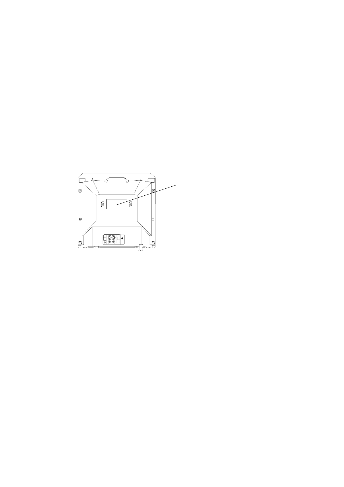
Location of the required Marking
The rating sheet and the safety caution are on the rear of the unit.
CERTIFICATION: COMPLIES WITH FDA
RADIA TION PERFORMANCE STANDARDS,
21 CFR SUBCHAPTER J.
A1-1
Page 3
SERVICING NOTICES ON CHECKING
As for the places which need special attentions,
they are indicated with the labels or seals on the
cabinet, chassis and parts. Make sure to keep the
indications and notices in the operation manual.
2. AVOID AN ELECTRIC SHOCK
There is a high voltage part inside. Avoid an
electric shock while the electric current is
flowing.
3. USE THE DESIGNATED PARTS
The parts in this equipment have the specific
characters of incombustibility and withstand
voltage for safety. Therefore, the part which is
replaced should be used the part which has
the same character.
Especially as to the important parts for safety
which is indicated in the circuit diagram or the
table of parts as a mark, the designated
parts must be used.
4. PUT PARTS AND WIRES IN THE
ORIGINAL POSITION AFTER
ASSEMBLING OR WIRING
There are parts which use the insulation
material such as a tube or tape for safety, or
which are assembled in the condition that
these do not contact with the printed board.
The inside wiring is designed not to get closer
to the pyrogenic parts and high voltage parts.
Therefore, put these parts in the original
positions.
5. TAKE CARE TO DEAL WITH THE
CATHODE-RAY TUBE
In the condition that an explosion-proof cathoderay tube is set in this equipment, safety is
secured against implosion. However, when
removing it or serving from backward, it is
dangerous to give a shock. Take enough care to
deal with it.
6. AVOID AN X-RAY1. KEEP THE NOTICES
Safety is secured against an X-ray by considering about the cathode-ray tube and the high
voltage peripheral circuit, etc.
Therefore, when repairing the high voltage peripheral circuit, use the designated parts and
make sure not modify the circuit.
Repairing except indicates causes rising of high
voltage, and it emits an X-ray from the cathoderay tube.
PERFORM A SAFETY CHECK AFTER
7.
SERVICING
Confirm that the screws, parts and wiring which
were removed in order to service are put in the
original positions, or whether there are the
portions which are deteriorated around the
serviced places serviced or not. Check the
insulation between the antenna terminal or
external metal and the AC cord plug blades.
And be sure the safety of that.
(INSULATION CHECK PROCEDURE)
1.
Unplug the plug from the AC outlet.
2.
Remove the antenna terminal on TV and turn
on the TV.
3.
Insulation resistance between the cord plug
terminals and the eternal exposure metal
[Note 2] should be more than 1M ohm by
using the 500V insulation resistance meter
[Note 1].
4.
If the insulation resistance is less than 1M
ohm, the inspection repair should be
required.
[Note 1]
If you have not the 500V insulation
resistance meter, use a Tester.
[Note 2]
External exposure metal: Antenna terminal
Earphone jack
HOW TO ORDER PARTS
Please include the following informations when you order parts. (Particularly the VERSION LETTER.)
1. MODEL NUMBER and VERSION LETTER
The MODEL NUMBER can be found on the back of each product and the VERSION LETTER can be
found at the end of the SERIAL NUMBER.
2. PART NO. and DESCRIPTION
You can find it in your SERVICE MANUAL.
A1-2
Page 4

IMPORTANT SAFEGUARDS
1.
READ INSTRUCTIONS
All the safety and operating instructions should be read before the unit is operated.
2.
RETAIN INSTRUCTIONS
The safety and operating instructions should be retained for future reference.
3.
HEED WARNINGS
All warnings on the unit and in the operating instructions should be adhered to.
4.
FOLLOW INSTRUCTIONS
All operating and use instructions should be followed.
5.
CLEANING
Unplug this unit from the wall outlet before cleaning. Do not use liquid cleaners or aerosol cleaners. Use a damp cloth for cleaning.
6.
ATTACHMENTS
Do not use attachments not recommended by the unit’s manufacturer as they may cause hazards.
7.
WATER AND MOISTURE
Do not use this unit near water. For example, near a bathtub, washbowl, kitchen sink, or laundry tub, in a wet basement, or near a
swimming pool.
8.
ACCESSORIES
Do not place this unit on an unstable cart, stand, tripod, bracket, or table. The unit may fall,
causing serious injury, and serious damage to the unit. Use only with a cart, stand, tripod,
bracket, or table recommended by the manufacturer.
8A.
An appliance and cart combination should be moved with care. Quick stops, excessive force,
and uneven surfaces may cause the appliance and cart combination to overturn.
9.
VENTILATION
Slots and openings in the cabinet and in the back or bottom are provided for ventilation, to ensure reliable operation of the unit, and
to protect it from overheating. These openings must not be blocked or covered. The openings should never be blocked by placing
the unit on a bed, sofa, rug, or other similar surface. This unit should never be placed near or over a radiator or heat source. This
unit should not be placed in a built-in installation such as a bookcase or rack unless proper ventilation is provided or the manufacturer’s instructions have been adhered to.
10.
POWER SOURCES
This unit should be operated only from the type of power source indicated on the rating plate. If you are not sure of the type of
power supply to your home, consult your appliance dealer or local power company. For units intended to operate from battery
power, or other sources, refer to the operating instructions.
11.
GROUNDING OR POLARIZATION
This unit is equipped with a polarized alternating-current line plug (a plug having one blade wider than the other). This plug will fit
into the power outlet only one way. This is a safety feature. If you are unable to insert the plug fully into the outlet, try reversing the
plug. If the plug should still fail to fit, contact your electrician to replace your obsolete outlet. Do not defeat the safety purpose of the
polarized plug. If your unit is equipped with a 3-wire grounding-type plug, a plug having a third (grounding) pin, this plug will only fit
into a grounding-type power outlet. This too, is a safety feature. If you are unable to insert the plug into the outlet, contact your
electrician to replace your obsolete outlet. Do not defeat the safety purpose of the grounding-type plug.
12.
POWER-CORD PROTECTION
Power-supply cords should be routed so that they are not likely to be walked on or pinched by items placed upon or against them,
paying particular attention to cords at plugs, convenience receptacles, and the point where they exit from the appliance.
13.
LIGHTNING
To protect your unit from a lightning storm, or when it is left unattended and unused for long periods of time, unplug it from the wall
outlet and disconnect the antenna or cable system. This will prevent damage to the unit due to lightning and power line surges.
14.
POWER LINES
An outside antenna system should not be located in the vicinity of overhead power lines or other electric light or power circuits, or
where it can fall into such power lines or circuits. When installing an outside antenna system, extreme care should be taken to keep
from touching such power lines or circuits, as contact with them might be fatal.
15.
OVERLOADING
Do not overload wall outlets and extension cords, as this can result in a risk of fire or electric shock.
16.
OBJECT AND LIQUID ENTRY
Do not push objects through any openings in this unit, as they may touch dangerous voltage points or short out parts that could
result in fire or electric shock. Never spill or spray any type of liquid into the unit.
17.
OUTDOOR ANTENNA GROUNDING
If an outside antenna or cable system is connected to the unit, be sure the antenna or cable system is grounded so as to provide
some protection against voltage surges and built-up static charges. Section 810 of the National Electrical Code, ANSI/NFPA 70,
provides information with respect to proper grounding of the mast and supporting structure, grounding of the lead-in wire to an
antenna discharge unit, size of grounding conductors, location of antenna discharge unit, connection to grounding electrodes, and
requirements for the grounding electrode.
18.
SERVICING
Do not attempt to service this unit yourself as opening or removing covers may expose you to dangerous voltage or other hazards.
Refer all servicing to qualified service personnel.
PORT ABLE CAR T WARNING
(symbol provided by RETAC)
S3126A
A1-3
Page 5

IMPORTANT SAFEGUARDS (CONTINUED)
DAMAGE REQUIRING SERVICE
19.
Unplug this unit from the wall outlet and refer servicing to qualified service personnel under the following conditions:
a.
When the power-supply cord or plug is damaged.
b.
If liquid has been spilled, or objects have fallen into the unit.
c.
If the unit has been exposed to rain or water.
d.
If the unit does not operate normally by following the operating instructions. Adjust only those controls that are covered by
the operating instructions, as an improper adjustment of other controls may result in damage and will often require extensive
work by a qualified technician to restore the unit to its normal operation.
e.
If the unit has been dropped or the cabinet has been damaged.
f.
When the unit exhibits a distinct change in performance, this indicates a need for service.
REPLACEMENT PARTS
20.
When replacement parts are required, be sure the service technician uses replacement parts specified by the manufacturer or
those that have the same characteristics as the original parts.
Unauthorized substitutions may result in fire, electric shock or other hazards.
SAFETY CHECK
21.
Upon completion of any service or repairs to this unit, ask the service technician to perform safety checks to determine that the unit
is in proper operating condition.
WALL OR CEILING MOUNTING
22.
The product should be mounted to a wall or ceiling only as recommended by the manufacturer.
HEAT
23.
The product should be situated away from heat sources such as radiators, heat registers, stoves, or other products (including
amplifiers) that produce heat.
DISC TRAY
24.
Keep your fingers well clear of the disc tray as it is closing. It may cause serious personal injury .
CONNECTING
25.
When you connect the product to other equipment, turn off the power and unplug all of the equipment from the wall outlet. Failure
to do so may cause an electric shock and serious personal injury. Read the owner's manual of the other equipment carefully and
follow the instructions when making any connections.
SOUND VOLUME
26.
Reduce the volume to the minimum level before you turn on the product. Otherwise, sudden high volume sound may cause hearing
or speaker damage.
SOUND DISTORTION
27.
Do not allow the product output distorted sound for a longtime. It may cause speaker overheating and fire.
HEADPHONES
28.
When you use the headphones, keep the volume at a moderate level. If you use the headphones continuously with high volume
sound, it may cause hearing damage.
LEASER BEAM
29.
Do not look into the opening of the disc tray or ventilation opening of the product to see the source of the laser beam. It may cause
sight damage.
DISC
30.
Do not use a cracked, deformed, or repaired disc. These discs are easily broken and may cause serious personal injury and
product malfunction.
NOTE TO CATV SYSTEM INSTALLER
31.
This reminder is provided to call the CATV system installer’s attention to Article 820-40 of the NEC that provides guidelines for
proper grounding and, in particular, specifies that the cable ground shall be connected to the grounding system of the building, as
close to the point of cable entry as practical.
EXAMPLE OF ANTENNA GROUNDING AS PER THE NATIONAL ELECTRICAL CODE
GROUND CLAMP
ELECTRIC SERVICE
EQUIPMENT
NEC-NATIONAL ELECTRICAL CODE
S2898A
ANTENNA LEAD IN WIRE
ANTENNA DISCHARGE UNIT
(NEC SECTION 810-20)
GROUND CLAMPS
GROUND CLAMPS
POWER SERVICE GROUNDING ELECTRODE SYSTEM
(NEC ART 250, PART H)
A1-4
Page 6
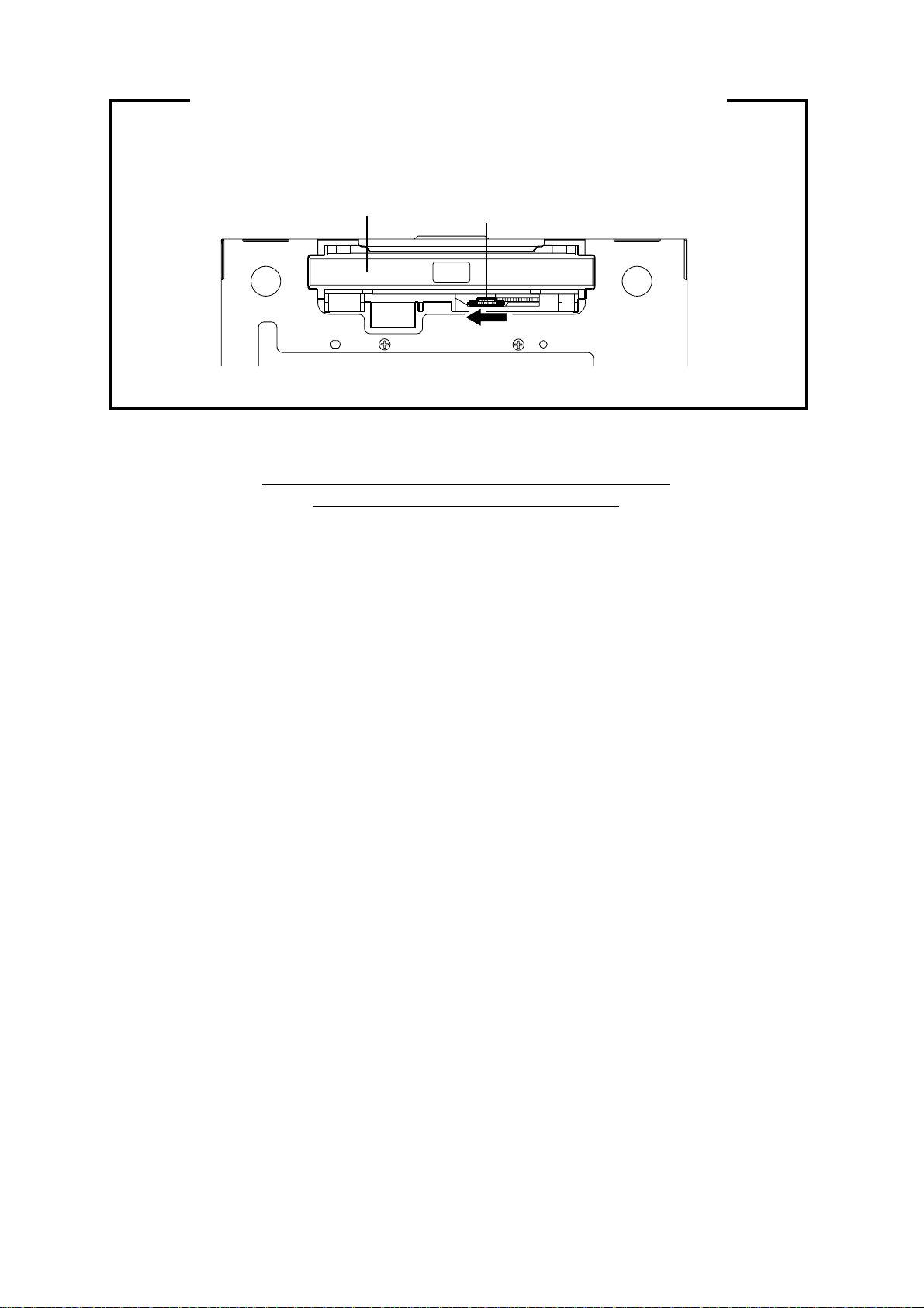
DISC REMOVAL METHOD AT NO POWER SUPPLY
1.2.Remove the Back Cabinet and TV/DVD Block. (Refer to item 1 of the DISASSEMBLY
INSTRUCTIONS.)
Rotate the white gear of Deck CD section in the direction of the arrow by hand, remove the disc from
Deck CD. (Refer to Fig. 1)
Deck CD
Gear (White)
Fig. 1
PARENTAL CONTROL - RATING LEVEL
4 DIGIT PASSWORD CANCELLATION
If the stored 4 digit password in the Rating Level menu needs to be cancelled, please follow the steps below.
Turn Unit ON.
1.
Confirm that no disc on the disc tray.
2.
Press and hold the '7' key on the remote control unit.
3.
Simultaneously press and hold the 'STOP' key on the front panel.
4.
Hold both keys for more than 3 seconds.
5.
The On Screen Display message 'Initialize' will appear.
6.
The 4 digit password has now been cleared.
7.
NB: The above procedure will reset ALL of the player's settings to the default factory state.
A1-5
Page 7

TABLE OF CONTENTS
CAUTION ................................................................................................................................
SERVICING NOTHCES CHECKING......................................................................................
HOW TO ORDER PARTS ......................................................................................................
IMPORTANT SAFEGUARDS.................................................................................................
DISC REMOVAL METHOD AT NO POWER SUPPLY...........................................................
PARENTAL CONTROL-RATING LEVEL ...............................................................................
TABLE OF CONTENTS..........................................................................................................
GENERAL SPECIFICATIONS................................................................................................
DISASSEMBLY INSTRUCTIONS
1.REMOVAL OF MECHANICAL PARTS AND P.C. BOARDS ............................................
2.REMOVAL OF ANODE CAP ............................................................................................
3.REMOVAL AND INSTALLATION OF FLAT PACKAGE IC...............................................
SERVICE MODE LIST.............................................................................................................
CONFIRMATION OF HOURS USED ......................................................................................
WHEN REPLACING EEPROM (MEMORY) IC .......................................................................
SERVICING FIXTURES AND TOOLS ....................................................................................
ELECTRICAL ADJUSTMENTS ..............................................................................................
BLOCK DIAGRAMS
TV.........................................................................................................................................
DVD FRONT/BACK END.....................................................................................................
POWER................................................................................................................................
PRINTED CIRCUIT BOARDS
DVD......................................................................................................................................
AV/CRT ................................................................................................................................
OPERATION/POWER .........................................................................................................
SCHEMATIC DIAGRAMS
MPEG...................................................................................................................................
MEMORY .............................................................................................................................
SYSCON1 ............................................................................................................................
DSP......................................................................................................................................
MOTOR DRIVE ....................................................................................................................
READ CHANNEL .................................................................................................................
AUDIO/VIDEO .....................................................................................................................
REGULATOR.......................................................................................................................
MICON/TUNER ....................................................................................................................
VIF/SIF/CHROMA ................................................................................................................
SOUND AMP .......................................................................................................................
IN/OUT .................................................................................................................................
AV SW..................................................................................................................................
COMB FILTER .....................................................................................................................
STEREO ..............................................................................................................................
DEFLECTION ......................................................................................................................
CRT......................................................................................................................................
POWER................................................................................................................................
OPERATION ........................................................................................................................
INTERCONNECTION DIAGRAM ............................................................................................
WAVEFORMS .........................................................................................................................
MECHANICAL EXPLODED VIEW ..........................................................................................
MECHANICAL REPLACEMENT PARTS LIST ......................................................................
ELECTRICAL REPLACEMENT PARTS LIST ........................................................................
A1-1
A1-2
A1-2
A1-3, A1-4
A1-5
A1-5
A2-1
A3-1~A3-6
B1-1, B1-2
B2-1
B3-1, B3-2
C-1
C-1
C-2
C-2
D-1~D-6
E-1, E-2
E-3, E-4
E-5, E-6
F-1, F-2
F-3~F-6
F-7, F-8
G-1, G-2
G-3, G-4
G-5, G-6
G-7, G-8
G-9, G-10
G-11, G-12
G-13, G-14
G-15, G-16
G-17, G-18
G-19, G-20
G-21, G-22
G-23, G-24
G-25, G-26
G-27, G-28
G-29, G-30
G-31, G-32
G-33, G-34
G-35, G-36
G-37, G-38
G-39, G-40
H-1~H-3
I-1, I-2
J1-1
J2-1~J2-6
A2-1
Page 8

GENERAL SPECIFICATIONS
G-1 TV CRT CRT Size / Visual Size 20 inch / 508.0 mmV
System CRT Type Flat
Color System NTSC
Speaker 2 Speaker
Sound Output Max 2.5W + 2.5W
G-2 DVD System Color System NTSC
Disc DVD, CD-DA, CD-R/RW, Video CD
Disc Diameter
Deck Disc Loading System Front Loading
Pick up 1-Lens 2-Beams System
Playback time(Max) DVD 1-Layer 135min (4.7GB)
Search speed Fwd 2-20 times / 4 step
Slow speed Fwd 1/7-1/2 times
G-3 Tuning Broadcasting System US System M
System Tuner and System 1Tuner
Receive CH Destination US(w/CATV)
Intermediate Picture(FP) 45.75MHz
Frequency Sound(FS) 41.25MHz
Preset CH No
Stereo/Dual TV Sound US-Stereo
Tuner Sound Muting Yes
G-4 Signal Video Signal Input Level 1 V p-p/75 ohm
RGB Signal Output Level Audio Signal Input Level -8.0dBm/50k ohm
G-5 Power Power Source AC 120V, 60Hz
Power Consumption at AC 110W at 120V 60Hz
Protector Power Fuse Yes
G-6 Regulation Safety UL
G-7 Temperature Operation
G-8 Operating Humidity Less than 80% RH
Deflection 90 degree
Magnetic Field BV/BH +0.45G / 0.18G
Position Front
Size 3 inch
Impedance 8 ohm
10%(Typical) 2.0W + 2.0W
120 mm , 80 mm
Motor 3 Motors
DVD 2-Layer 245min (8.5GB)
CD 74min
Video CD 74min
Actual 2-45 times (DVD, Video CD)
4-40 times (CD)
Rev 2-20 times / 4 step
Actual 2-45 times (DVD, Video CD)
4-40 times (CD)
Actual --
Actual 1-2 times
Tuning System F-Synth
Input Impedance VHF/UHF 75 Ohm
CH Coverage
FP-FS 4.50MHz
Output Level 1 V p-p/75 ohm
S/N Ratio (Weighted) 65dB
Horizontal Resolution at DVD Mode 400 Lines (TV Monitor)
Output Level -8.0dBm/1k ohm
Digital Output Level 0.5 V p-p/75 ohm
S/N Ratio at DVD (Weighted) 90 dB
Harmonic Distortion 0.06% (1kHz)
Frequency Response : at DVD 4Hz - 22kHz
at Video CD 4Hz - 20kHz
at CD 4Hz - 20kHz
DC --
at DC -Stand by (at AC) 5 W at 120V 60Hz
Per Year -- kWh/Year
Radiation FCC
X-Radiation DHHS
Laser DHHS
Storage
Rev 1/7-1/2 times
2~69, 4A, A-5~A-1, A~I, J~W, W+1~W+84
500 Lines ( Video Out)
o
C ~ +40oC
+5
o
C ~ +60oC
-20
A3-1
Page 9

GENERAL SPECIFICATIONS
G-9 On Screen Menu(TV) Yes
Display Menu Type Icon
Picture Yes
Brightness Yes
Contrast Yes
Color Yes
Tint Yes
Sound Yes
CH Yes
Option Yes
Clock No
Clock Set No
On/Off Timer No
Sleep Timer Yes
CH/AV/DVD Yes
Stereo/Audio Output Yes
Caption / Text Yes
Auto Search/Position No
Game Yes
Volume Yes
Muting No
Sharpness Yes
Bass Yes
Treble Yes
Balance Yes
TV/CATV
Add/Delete
Auto CH Memory
V-Chip Yes
Language Yes
Bilingual No
SAP Yes
Yes
Yes
Yes
A3-2
Page 10

GENERAL SPECIFICATIONS
G-10 On Screen Menu (DVD) Yes
Display Menu Type Character
G-11 OSD Language (TV) Eng, Fre, Spa
(DVD) Eng, Fre, Spa
Language Yes
Menu Yes
Subtitle Yes
Audio Yes
Picture Yes
TV Screen Size Yes
OSD Display On/Off Yes
Sound Yes
DRC (Dynamic Range Control) Yes
dts Decode No
Output(5.1ch/ 2ch) No
Surround On/Off No
Center On/Off No
Sub Woofer On/Off No
Parental Yes
Password Lock/ Un Lock Yes
Rating Level Yes
Other Yes
OSD Language(Set up Language) Yes
Output(RGB/Composite) No
Open Yes
Close Yes
No disc Yes
Reading Yes
Play Yes
Still/Pause Yes
Stop Yes
Prohibit Mark Yes
Step Yes
Next Yes
Back Yes
Random Yes (CD, Video CD)
Repeat Yes
Slow+ ## Yes
Slow- ## Yes
Search+ ## Yes
Search- ## Yes
Jump Yes
Resume Yes
Title No. Yes
Chapter No. Yes
Track No. Yes
Time Yes
Sub Title No. Yes
Angle No. Yes
Vocal On/Off Yes
Audio No. Yes
Audio Stereo L/R Yes (Video CD)
Zoom Yes
Marker No. No
Program Play Back Yes (CD, Video CD)
Surround On/Off No
Screen Saver No
MP3 File Name No
File No No
Time No
Track No No
A3-3
Page 11

GENERAL SPECIFICATIONS
G-12 Remote Unit RC-EF
Control Glow in Dark Remocon Yes
Format NEC
Custom Code 71-8E h
Power Source Voltage(D.C) 3V
Total Keys 45 Key
Keys Power Yes
UM size x pcs UM-4 x 2 pcs
1 Yes
2 Yes
3 Yes
4 Yes
5 Yes
6 Yes
7 Yes
8 Yes
9 Yes
0 Yes
Play Yes
Stop Yes
Search+ Yes
Search- Yes
Skip+ Yes
Skip- Yes
Slow+ Yes
Slow- Yes
Pause Yes
Call Yes
TV/DVD Yes
Cancel Yes
Audio Select Yes
Angle Yes
Subtitle Yes
Top Menu Yes
Set up/ Menu Yes
DVD Menu Yes
Return Yes
Up/ Set+/ CH Up Yes
Down/ Set-/ CH Down Yes
Left/ Select- Yes
Right/ Select+ Yes
Select/ Enter Yes
Play Mode Yes
Closed Caption Yes
Input Select Yes
Volume+ Yes
Volume- Yes
Repeat A-B Yes
Zoom/ Quick View Yes
Sleep Yes
Jump Yes
Game Yes
A3-4
Page 12
GENERAL SPECIFICATIONS
G-13 Features CATV Yes
G-14 Accessories Owner's Manual Language English
Auto Shut Off Yes
Auto Clock No
Just Clock No
Auto CH Memory Yes
V-Chip USA V-chip Yes
CANADA V-chip No
Auto Search No
SAP Yes
Game Position Yes
FM Transmitter No
Energy Star No
Closed Caption Yes
Comb Filter Yes
Protect of FBT Leak Circuit Yes
Choke Coil No
Power On Memory No
Parental Lock (DVD Only) Yes
Video CD Playback Yes
MP3 Playback No
Digital Out (Dolby Digital) Yes
(MPEG) Yes
(PCM) Yes
(DTS) Yes
Down Mix Out (Dolby Digital) Yes
(DTS) No
Surround (Spatializer N-2-2) No
Screen Saver No
w/Guarantee Card Yes
Buyer Model No MD20FM1R
Remote Control Unit Yes
Battery Yes
UM size x pcs UM-4 x 2 pcs
OEM Brand No
Rod Antenna No
Poles No
Terminal --
Loop Antenna No
Terminal --
U/V Mixer No
300 ohm to 75 ohm Antenna Adapter Yes
Antenna Change Plug No
Guarantee Card No
Registration Card Yes
Warranty Card No
ESP Card No
Service Station List No
DC Car Cord (Center+) No
Columbia Offer Sheet No
A3-5
Page 13
GENERAL SPECIFICATIONS
G-15 Interface Switch Front Power (Tact) Yes
Rear Main Power SW No
Indicator Power Red
Terminals Front Video Input RCA x 1
Rear Video Input RCA x 1
G-16 Set Size Approx. W x D x H (mm) 574x483x514.5
G-17 Weight Net (Approx.) 25.5kg (56.1lbs)
G-18 Carton Master Carton No
Gift Box Yes
Drop Test
Container Stuffing (40' container) 171 Sets
G-19 Cabinet Material Cabinet Front PS 94V0 DECABROM
Channel Up Yes
Channel Down Yes
Volume Up Yes
Volume Down Yes
Play Yes
Open/Close Yes
Skip(>>) Yes
Skip(<<) Yes
Still/Pause No
Stop Yes
Main Power SW No
Stand-by No
On Timer No
Audio Input RCA x 2(Stereo)
Other Terminal Head Phone
Audio Input RCA x 2(Stereo)
Video Output RCA x 1
Audio Output RCA x 2(Stereo)
Digital Audio Output Coaxial (DVD Only)
Diversity No
DC Jack 12V(Center +) No
VHF/UHF Antenna Input F Type
Gross (Approx.) 29.0kg (63.8lbs)
Content --- Sets
Material --- / --Dimensions W x D x H(mm) --Description of Origin ---
Material Double/White
W/Color Photo Label No
Dimensions W x D x H(mm) 647x620x625
Design As Per Buyer 's
Description of Origin Yes
Natural Dropping At 1 Corner / 3 Edges / 6 Surfaces
Height (cm) 31
Cabinet Rear PS 94V0 DECABROM
A3-6
Page 14

DISASSEMBLY INSTRUCTIONS
1. REMOVAL OF MECHANICAL PARTS
AND P.C. BOARDS
1-1: BACK CABINET (Refer to Fig. 1-1)
1.
Remove the 7 screws 1.
2.
Remove the screw 2 which are used for holding the
Back Cabinet.
3.
Remove the AC cord from the AC cord hook 3.
4.
Remove the Back Cabinet in the direction of arrow.
Front Cabinet
1
1
1
1
2
1-2: CRT PCB (Refer to Fig. 1-2)
CAUTION: BEFORE REMOVING THE ANODE CAP,
DISCHARGE ELECTRICITY BECAUSE IT
CONTAINS HIGH VOLTAGE.
BEFORE ATTEMPTING TO REMOVE OR
REPAIR ANY PCB, UNPLUG THE POWER
CORD FROM THE AC SOURCE.
1.
Remove the Anode Cap.
(Refer to REMOVAL OF ANODE CAP)
2.
Disconnect the following connectors:
(CP801 and CP805).
3.
Remove the CRT PCB in the direction of arrow.
Front Cabinet
1
1
3
Back Cabinet
1
Fig. 1-1
CRT PCB
1-3: POWER PCB/DVD BLOCK (Refer to Fig. 1-3)
1.
Remove the 2 screws 1.
2.
Disconnect the following connectors:
(CP102, CP303, CP401 and CP3800).
3.
Remove the POWER PCB/DVD Block in the direction of
arrow.
1
Front Cabinet
Power PCB/DVD Block
Fig. 1-3
1-4: POWER PCB (Refer to Fig. 1-4)
1.
Remove the 11 screws 1.
2.
Remove the Top Shield in the direction of arrow (A).
3.
Disconnect the following connectors:
(CP3802 and CP3803).
4.
Remove the screw 2.
5.
Remove the PCB Cover Ass'y in the direction of arrow (B).
6.
Remove the screw 3.
7.
Remove the Power PCB in the direction of arrow (C).
3
PCB Cover Ass'y
1
1
1
1
1
1
1
1
1
1
1
(A)
(C)
2
(B)
1
Fig. 1-2
Fig. 1-4
B1-1
Page 15

DISASSEMBLY INSTRUCTIONS
1-5: AV PCB/DVD PCB/DECK CD (Refer to Fig. 1-5)
1.
Make the short circuit on the position as shown Fig. 1-5
using a soldering. If you remove the Deck CD with no
soldering, the Laser may be damaged.
2.
Disconnect the following connectors:
(CP8001, CP8002 and CP8005).
3.
Remove the 4 screws 1.
4.
Remove the Deck Angle in the direction of arrow (A).
5.
Disconnect the following connectors:
(CP2301, CP2302 and CP2601).
6.
Remove the 4 screws 2.
7.
Remove the Deck CD in the direction of arrow (B).
8.
Remove the 4 screws 3.
9.
Remove the DVD PCB in the direction of arrow (C).
10.
Remove the 3 screws 4.
11.
Remove the AV PCB in the direction of arrow (D).
Pick Up PCB
2
2
Deck CD
2
2
3
DVD PCB
1
AV PCB
3
1
1
(B)
3
(C)
(A)
(D)
Bottom Plate
Make the sort circuit
using a soldering.
3
1
Deck Angle
4
4
4
Fig. 1-5
NOTE
When the installation of the Deck CD, remove all the
soldering on the short circuit position after the connection of
Pick Up PCB and DVD PCB connector.
B1-2
Page 16
DISASSEMBLY INSTRUCTIONS
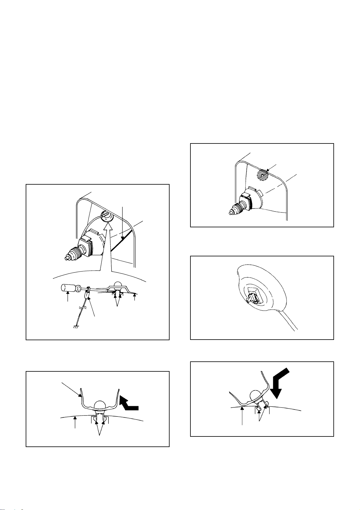
2. REMOVAL OF ANODE CAP
Read the following NOTED items before starting work.
After turning the power off there might still be a potential
*
voltage that is very dangerous. When removing the
Anode Cap, make sure to discharge the Anode Cap's
potential voltage.
*
Do not use pliers to loosen or tighten the Anode Cap
terminal, this may cause the spring to be damaged.
REMOVAL
1. Follow the steps as follows to discharge the Anode Cap.
(Refer to Fig. 2-1.)
Connect one end of an Alligator Clip to the metal part of a
flat-blade screwdriver and the other end to ground.
While holding the plastic part of the insulated Screwdriver,
touch the support of the Anode with the tip of the
Screwdriver.
A cracking noise will be heard as the voltage is discharged.
GND on the CRT
3. After one side is removed, pull in the opposite direction
to remove the other.
NOTE
Take care not to damage the Rubber Cap.
INSTALLATION
1. Clean the spot where the cap was located with a small
amount of alcohol. (Refer to Fig. 2-3.)
NOTE
Confirm that there is no dirt, dust, etc. at the spot where
the cap was located.
Location of Anode Cap
Fig. 2-3
Screwdriver
Alligator Clip
GND on the CRT
Flip up the sides of the Rubber Cap in the direction of
2.
the arrow and remove one side of the support.
(Refer to Fig. 2-2.)
Rubber Cap
Support
CRT
Fig. 2-1
2.3.Arrange the wire of the Anode Cap and make sure the
wire is not twisted.
Turn over the Rubber Cap. (Refer to Fig. 2-4.)
Fig. 2-4
4. Insert one end of the Anode Support into the anode
button, then the other as shown in Fig. 2-5.
CRT
Support
Fig. 2-2
Support
CRT
5.6.Confirm that the Support is securely connected.
Put on the Rubber Cap without moving any parts.
B2-1
Fig. 2-5
Page 17
DISASSEMBLY INSTRUCTIONS
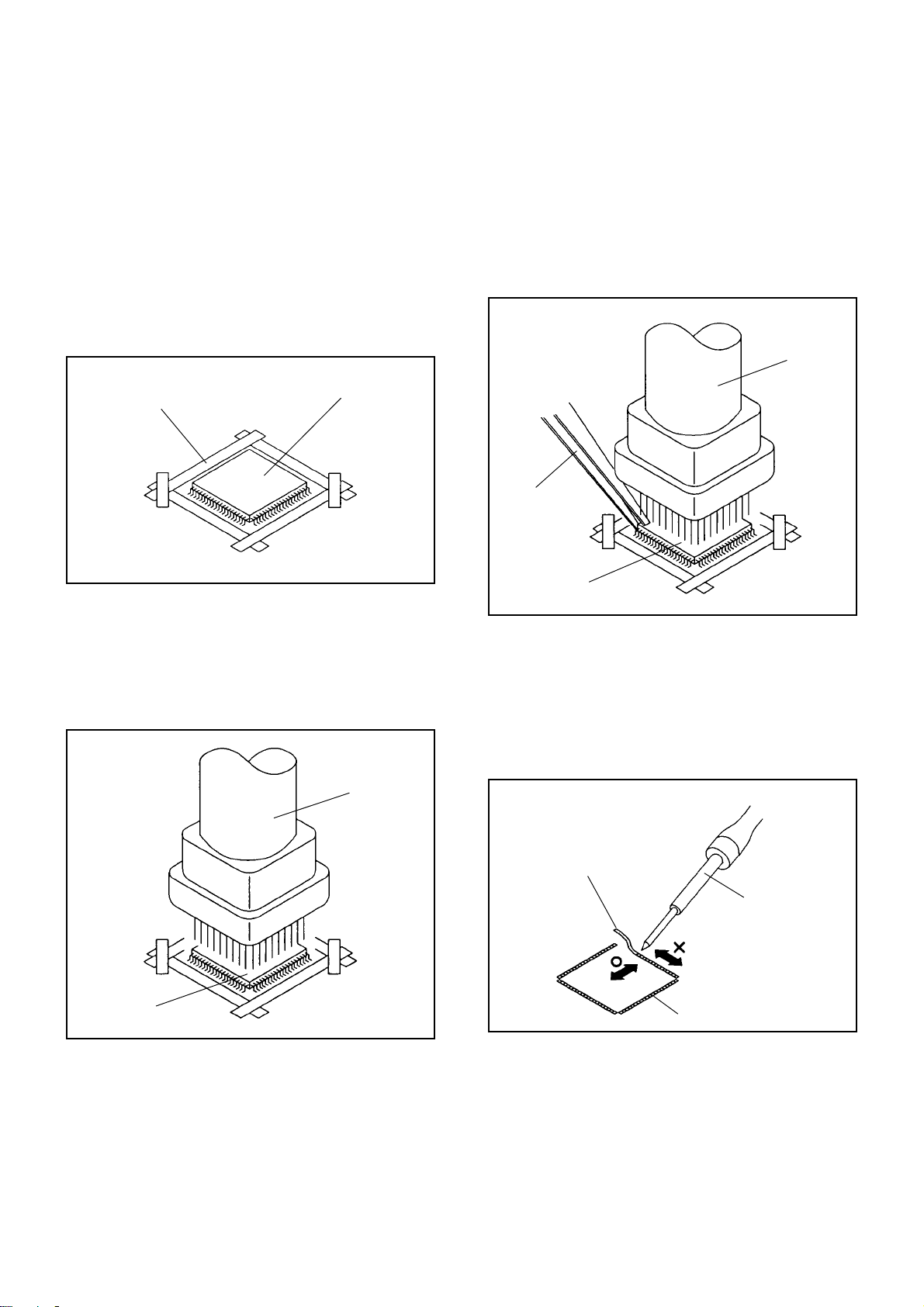
3.
REMOVAL AND INSTALLATION OF
FLAT PACKAGE IC
REMOVAL
Put the Masking Tape (cotton tape) around the Flat
1.
Package IC to protect other parts from any damage.
(Refer to Fig. 3-1.)
NOTE
Masking is carried out on all the parts located within
10 mm distance from IC leads.
When IC starts moving back and forth easily after
3.
desoldering completely, pickup the corner of the IC using
a tweezers and remove the IC by moving with the IC
desoldering machine. (Refer to Fig. 3-3.)
NOTE
Some ICs on the PCB are affixed with glue, so be
careful not to break or damage the foil of each IC
leads or solder lands under the IC when removing it.
Blower type IC
desoldering
machine
Masking Tape
(Cotton Tape)
Heat the IC leads using a blower type IC desoldering
2.
IC
machine. (Refer to Fig. 3-2.)
NOTE
Do not add the rotating and the back and forth
directions force on the IC, until IC can move back and
forth easily after desoldering the IC leads completely.
Blower type IC
desoldering machine
Fig. 3-1
Tweezers
IC
Peel off the Masking Tape.4.
Absorb the solder left on the pattern using the Braided
5.
Shield Wire. (Refer to Fig. 3-4.)
NOTE
Do not move the Braided Shield Wire in the vertical
direction towards the IC pattern.
Fig. 3-3
Braided Shield Wire
Soldering Iron
IC
Fig. 3-2
IC pattern
Fig. 3-4
B3-1
Page 18

DISASSEMBLY INSTRUCTIONS
INSTALLATION
Take care of the polarity of new IC and then install the
1.
new IC fitting on the printed circuit pattern. Then solder
each lead on the diagonal positions of IC temporarily.
(Refer to Fig. 3-5.)
Soldering Iron
Solder temporarily
Supply the solder from the upper position of IC leads
2.
Solder temporarily
sliding to the lower position of the IC leads.
(Refer to Fig. 3-6.)
Fig. 3-5
When bridge-soldering between terminals and/or the
4.
soldering amount are not enough, resolder using a Thintip Soldering Iron. (Refer to Fig. 3-8.)
Thin-tip Soldering Iron
IC
Fig. 3-8
Finally, confirm the soldering status on four sides of the
5.
IC using a magnifying glass.
Confirm that no abnormality is found on the soldering
position and installation position of the parts around the
IC. If some abnormality is found, correct by resoldering.
NOTE
When the IC leads are bent during soldering and/or
repairing, do not repair the bending of leads. If the
bending of leads are repaired, the pattern may be
damaged. So, be always sure to replace the IC in this
case.
Soldering IronSolder
IC
Absorb the solder left on the lead using the Braided
3.
Supply soldering
from upper position
to lower position
Shield Wire. (Refer to Fig. 3-7.)
NOTE
Do not absorb the solder to excess.
Soldering Iron
IC
Braided Shield Wire
Fig. 3-6
Fig. 3-7
B3-2
Page 19

SERVICE MODE LIST
This unit provided with the following SERVICE MODES so you can repair, examine and adjust easily.
To enter to the SERVICE MODE function, press and hold both buttons simultaneously on the main unit and on the remote
control for more than a standard time (second).
Set Key
VOL. (-) MIN
VOL. (-) MIN 1
VOL. (-) MIN 4
VOL. (-) MIN
VOL. (-) MIN
VOL. (-) MIN 9
Standard Time
(seconds)
0
6
8
1
1
1
1
1
1
Releasing of V-CHIP PASSWORD.
Initialization of the factory on TV.
NOTE:
Initialization of the factory on DVD.
NOTE: Do not use this for the normal servicing.
POWER ON total hours are displayed on the screen.
Refer to the "PREVENTIVE CHECKS AND SERVICE INTERVALS"
(CONFIRMATION OF HOURS USED).
Can be checked of the INITIAL DATA of MEMORY IC.
Refer to the "WHEN REPLACING EEPROM (MEMORY) IC".
Writing of EEPROM initial data.
NOTE: Do not use this for the normal servicing.
Display of the Adjustment MENU on the screen.
Refer to the "ELECTRICAL ADJUSTMENT" (On-Screen Display
Adjustment).
Do not use this for the normal servicing.
If you set a factory initialization, the memories are reset such as
the channel setting, and the POWER ON total hours.
The function will only work without the setting of DVD disc at
DVD mode.
While pressing the Remocon Key for more than the Standard
Time, press the Set Key simultaneously.
OperationsRemocon Key
Releasing of PARENTAL LOCK.
STOP 7 3
Refer to the “PARENTAL CONTROL - RATING LEVEL”.
NOTE:
The function will only work without the setting of DVD disc at
DVD mode.
CONFIRMATION OF HOURS USED
POWER ON total hours can be checked on the screen. Total hours are displayed in 16 system of notation.
NOTE: If you set a factory initialization, the total hours is reset to "0".
1.
Set the VOLUME to minimum.
2.
Press both VOL. DOWN button on the set and Channel
button (6) on the remote control for more than 1 second.
3.
After the confirmation of using hours, turn off the power.
ADDRESS DATA
INIT 00 F8
CRT ON 0010
FIG. 1
Initial setting content of MEMORY IC.
POWER ON total hours.
= (16 x 16 x 16 x thousands digit value)
+ (16 x 16 x hundreds digit value)
+ (16 x tens digit value)
+ (ones digit value)
C-1
Page 20

WHEN REPLACING EEPROM (MEMORY) IC
If a service repair is undertaken where it has been required to change the MEMORY IC, the following steps should be taken to
ensure correct data settings while making reference to TABLE 1.
Note: No need setting for the position of the mark @ due to the adjustment value.
+0 +1 +2 +3 +4 +5 +6 +7 +8 +9
INI
F8 43 25 01 F1 27 27 D7 81 CD
64 67 69 2A 6B 6C 6D 6E 6F
10 26 70 71 52 72 53 73
20 57 77 77 58 58 78
54 74 55 75 75 56 56 76 76 57
78 59 59 79 79 5A 5A 7A 7A 5B
30 5B 7B 7B 5C 5C 7C
40 5D 5F 5F 7F 7F @ @
7C 5D 7D 7D 5E 5E 7E 7E 5F
@ @@@@@@@@
50
60
70
1.
Enter DATA SET mode by setting VOLUME to minimum.
2.
Press both VOL. DOWN button on the set and Channel button (6) on the remote control for more than 1 second.
ADDRESS and DATA should appear as FIG 1.
@
@@@@@@@@@@ 0052094510
@
--- --- --- --- --- --- --- --- --- --- --- --- --- ------
80
Table 1
ADDRESS DATA
INIT 00 F8
CRT ON 0010
+A +B +C +D +E +F
D9 3F BF C0 61 6300
@@@@@@
FIG. 1
3.
ADDRESS is now selected and should "blink". Using the VOL. UP/DOWN button on the remote, step through the
ADDRESS until required ADDRESS to be changed is reached.
4.
Press ENTER to select DATA. When DATA is selected, it will "blink".
5.
Again, step through the DATA using VOL. UP/DOWN button until required DATA value has been selected.
6.
Pressing ENTER will take you back to ADDRESS for further selection if necessary.
7.
Repeat steps 3 to 6 until all data has been checked.
8.
When satisfied correct DATA has been entered, turn POWER off (return to STANDBY MODE) to finish DATA input.
After the data input, set to the initializing of shipping.
9.
Turn POWER on.
10.
While holding down VOLUME button on front cabinet, press key 1 on remote control for more than 1 second.
11.
After the finishing of the initializing of shipping, the unit will turn off automatically.
The unit will now have the correct DATA for the new MEMORY IC.
SERVICING FIXTURES AND TOOLS
JG175A
DVD Test Disc
(A-BEX TDV-540)
Ref. No.
JG175A
Part No.
APJG175A00
Parts Name
DVD Test Disc
(A-BEX TDV-540)
Remarks
Tint adjustment of DVD mode
C-2
Page 21

ELECTRICAL ADJUSTMENTS
1.
BEFORE MAKING ELECTRICAL
ADJUSTMENTS
Read and perform these adjustments when repairing the
circuits or replacing electrical parts or PCB assemblies.
CAUTION
•
Use an isolation transformer when performing any
service on this chassis.
•
Before removing the anode cap, discharge electricity
because it contains high voltage.
•
When removing a PCB or related component, after
unfastening or changing a wire, be sure to put the wire
back in its original position.
•
When you exchange IC and Transistor for a heat sink,
apply the silicon grease on the contact section of the
heat sink. Before applying new silicon grease, remove all
the old silicon grease. (Old grease may cause damages
to the IC and Transistor).
Prepare the following measurement tools for electrical
adjustments.
1. Oscilloscope
2. Digital Voltmeter
3. AC Voltmeter
4. Pattern Generator
5. Multi-Sound Signal Generator
NO.
FUNCTION
01
R CUT OFF
02
G CUT OFF
03
B CUT OFF
04
G DRIVE
05
B DRIVE
06
BRIGHTNESS(CENT.)
07
BRIGHTNESS(MAX)
08
BRIGHTNESS(MIN)
09
COLOR(CENT.)
10
COLOR(MAX)
11
COLOR(MIN)
12
TINT
13
SUB CONTRAST
14
CONTRAST(CENT.)
15
CONTRAST(MAX)
16
CONTRAST(MIN)
17
SHARPNESS
18
RGB CONTRAST
19
H POSITION
20
V POSITION
21
V SIZE
22
V LINEARITY
23
V S CORRECTION
24
EW PARABOLA CORR.
25
EW TRAPEZIUM CORR.
26
H SIZE
27
V EHT
28
H EHT
29
RF AGC
30
V CENTERING
31
CORNER CORR. TOP
32
CORNER CORR. BTM
33
OSD H
34
FM LEVEL
35
TEST PWM
36
TEST TONE CONTROL
FUNCTION
NO.
BRI. AV(CENT.)
37
BRI. AV(MAX)
38
BRI. AV(MIN)
39
COL. AV(CENT.)
40
COL. AV(MAX)
41
COL. AV(MIN)
42
TINT AV
43
SUB CONTRAST AV
44
CONT. AV(CENT.)
45
CONT. AV(MAX)
46
CONT. AV(MIN)
47
SHARPNESS AV
48
BRI. DVD(CENT.)
49
BRI. DVD(MAX)
50
BRI. DVD(MIN)
51
COL. DVD(CENT.)
52
COL. DVD(MAX)
53
COL. DVD(MIN)
54
TINT DVD
55
SUB CONTRAST DVD
56
CONT. DVD(CENT.)
57
CONT. DVD(MAX)
58
CONT. DVD(MIN)
59
SHARPNESS DVD
60
BRI. GAME(CENT.)
61
BRI. GAME(MAX)
62
BRI. GAME(MIN)
63
CONT. GAME(CENT.)
64
CONT. GAME(MAX)
65
CONT. GAME(MIN)
66
TUNING V MUTE
67
POWER ON V MUTE
68
INPUT LEVEL
69
SEPARATION L
70
SEPARATION H
71
CUT OFF
72
Fig. 1-2
On-Screen Display Adjustment
In the condition of NO indication on the screen.
1.
Press the VOL. DOWN button on the set and the
Channel button (9) on the remote control for more than
1 second to appear the adjustment mode on the screen
as shown in Fig. 1-1.
Function
Step No.
Use the Channel UP/DOWN button or Channel button
2.
01 RCUT
3E
(1-0) on the remote control to select the options shown
in Fig. 1-2.
Press the MENU button on the remote control to end
3.
the adjustments.
Fig. 1-1
2. BASIC ADJUSTMENTS
2-1: CONSTANT VOLTAGE
1.
Set condition is AV MODE without signal.
2.
Using the remote control, set the brightness and contrast
to normal position.
3.
Connect the digital voltmeter to TP3801.
4.
Adjust the VR3800 until the digital voltmeter is 115 ± 0.5V.
2-2: RF AGC
1.
Receive the VHF HIGH (63dB).
2.
Place the set with Aging Test for more than 15 minutes.
3.
Connect the digital voltmeter between the pin 5 of
CP101 and the pin 1 (GND) of CP101.
4.
Activate the adjustment mode display of Fig. 1-1 and
press the channel button (29) on the remote control to
select "AGC".
5.
Press the RIGHT/LEFT button on the remote control
until the digital voltmeter is 2.4 ± 0.05V.
2-3: FOCUS
1.
Receive the monoscope pattern.
2.
Turn the Focus Volume fully counterclockwise once.
3.
Adjust the Focus Volume until picture is distinct.
2-4: CUT OFF
1.
Adjust the unit to the following settings.
G DRIVE=3F, B DRIVE=3F, R CUT OFF=7F, G CUT
OFF=7F, B CUT OFF=7F
2.
Place the set with Aging Test for more than 15 minutes.
3.
Set condition is AV MODE without signal.
4.
Using the remote control, set the brightness and contrast
to normal position.
5.
Activate the adjustment mode display of Fig. 1-1 and
press the channel button (72) on the remote control to
select "CUT OFF".
6.
Adjust the Screen Volume until a dim raster is obtained.
D-1
Page 22

ELECTRICAL ADJUSTMENTS
2-5: WHITE BALANCE
NOTE: Adjust after performing CUT OFF adjustment.
1.
Place the set with Aging Test for more than 15 minutes.
2.
Receive the gray scale pattern from the Pattern
Generator.
3.
Using the remote control, set the brightness and
contrast to normal position.
4.
Activate the adjustment mode display of Fig. 1-1 and
press the channel button (04) on the remote control to
select "G DRV".
5.
Press the CH. UP/DOWN button on the remote control
to select the "R CUT", "G CUT", "B CUT", "G DRV" or
"B DRV".
6.
Adjust the RIGHT/LEFT button on the remote control to
whiten the R CUT, G CUT, B CUT, G DRV, and B DRV
at each step tone sections equally.
7.
Perform the above adjustments 5 and 6 until the white
color is looked like a white.
2-6: HORIZONTAL POSITION
1.
Receive the monoscope pattern.
2.
Using the remote control, set the brightness and
contrast to normal position.
3.
Activate the adjustment mode display of Fig. 1-1 and
press the channel button (19) on the remote control to
select "HPOSI".
4.
Press the RIGHT/LEFT button on the remote control
until the SHIFT quantity of the OVER SCAN on right
and left becomes minimum.
2-7: VERTICAL POSITION
1.
Receive the monoscope pattern.
2.
Using the remote control, set the brightness and
contrast to normal position.
3.
Activate the adjustment mode display of Fig. 1-1 and
press the channel button (20) on the remote control to
select "VPOSI".
4.
Check if the step No. V POSI is "02".
5.
Adjust the VR402 until the horizontal line becomes fit
to notch of the shadow mask.
2-8: VERTICAL SIZE
1.
Receive the monoscope pattern.
2.
Using the remote control, set the brightness and
contrast to normal position.
3.
Activate the adjustment mode display of Fig. 1-1 and
press the channel button (21) on the remote control to
select "VSIZE".
4.
Press the RIGHT/LEFT button on the remote control
until the Up/Down OVER SCAN Quantity becomes
equal to the Right/Left OVER SCAN Quantity.
5.
Receive a broadcast and check if the picture is normal.
2-9: VERTICAL LINEARITY
NOTE:
1.
2.
3.
4.
2-10: SEPARATION
Please do the method (1) or method (2) adjustment.
Method (1)
1.
2.
3.
4.
5.
6.
7.
Method (2)
1.
2.
3.
4.
5.
6.
7.
8.
9.
Adjust after performing adjustments in section 2-8.
After the adjustment of Vertical Linearity, reconfirm
the Vertical Position and Vertical Size adjustments.
Receive the monoscope pattern.
Using the remote control, set the brightness and
contrast to normal position.
Activate the adjustment mode display of Fig. 1-1 and
press the channel button (22) on the remote control to
select "VLIN".
Press the RIGHT/LEFT button on the remote control
until the SHIFT quantity of the OVER SCAN on upside
and downside becomes minimum.
Set the multi-sound signal generator for each different
L-ch and R-ch frequency (Ex. L-ch=2KHz, R-ch=400Hz)
and receive the RF signal.
Connect the oscilloscope to the Audio Out Jack.
Press the AUDIO button on the remote control to set to
the stereo mode.
Activate the adjustment mode display of Fig. 1-1 and
press the channel button (70) on the remote control to
select “SEPAL”.
Press the RIGHT/LEFT button on the remote control to
adjust it until the audio output wave becomes a fine
sine wave.
Press the CH UP button 1 time to set to "SEPAH"
mode.
Press the RIGHT/LEFT button on the remote control to
adjust it until the audio output wave becomes a fine
sine wave.
Set the multi-sound signal generator L-ch=1KHz, R-ch
=Non input and receive the RF signal.
Connect the oscilloscope to the Audio Out Jack (R-ch).
Press the AUDIO button on the remote control to set to
the stereo mode.
Activate the adjustment mode display of Fig. 1-1 and
press the channel button (70) on the remote control to
select “SEPAL”.
Press the RIGHT/LEFT button on the remote control to
adjust it until the R-ch output becomes minimum.
Press the CH UP button 1 time to set to "SEPAH" mode.
Press the RIGHT/LEFT button on the remote control to
adjust it until the R-ch output becomes minimum.
Set the multi-sound signal generator L-ch=Non input,
R-ch=1KHz and receive the RF signal.
Connect the oscilloscope to the Audio Out Jack (L-ch).
Then perform the above adjustments 3~7.
D-2
Page 23

ELECTRICAL ADJUSTMENTS
2-11: OSD HORIZONTAL
Activate the adjustment mode display of Fig. 1-1 and
1.
press the channel button (33) on the remote control to
select "OSD".
Press the RIGHT/LEFT button on the remote control
2.
until the difference of A and B becomes minimum.
(Refer to Fig. 2-1)
33 OSD
15
BA
2-12: LEVEL
1.
Receive the VHF HIGH (70dB).
2.
Connect the AC voltmeter to pin 6 of CP101.
3.
Activate the adjustment mode display of Fig. 1-1 and
press the channel button (69) on the remote control to
select "LVL".
4.
Press the RIGHT/LEFT button on the remote control
until the AC voltmeter is 72 ± 2mV.
2-13: SUB BRIGHT CENTER
1.
Receive the monoscope pattern. (RF Input)
2.
Using the remote control, set the brightness and
contrast to normal position.
3.
Activate the adjustment mode display of Fig. 1-1 and
press the channel button (06) on the remote control to
select "BRTC".
4.
Press the RIGHT/LEFT button on the remote control
until the white 15% is starting to be visible
5.
Receive the monoscope pattern. (Audio Video Input)
6.
Press the INPUT SELECT button on the remote control
to set to the AV mode.
7.
Using the remote control, set the brightness and
contrast to normal position.
8.
Activate the adjustment mode display of Fig. 1-1 and
press the channel button (37) on the remote control to
select "BRTCA".
9.
Press the RIGHT/LEFT button on the remote control
until the white 15% is starting to be visible
10.
Press the TV/DVD button on the remote control to set to
the DVD mode.
11.
Activate the adjustment mode display of Fig. 1-1 and
press the channel button (49) on the remote control to
select "BRTCD".
12.
Press the RIGHT/LEFT button on the remote control to
set the same step numbers as the AV.
13.
Press the GAME button on the remote control to set to
the GAME mode.
14.
Activate the adjustment mode display of Fig. 1-1 and
press the channel button (61) on the remote control to
select "BRTCG".
15.
Press the RIGHT/LEFT button on the remote control to
decrease the step numbers by 16 steps to the AV.
Fig. 2-1
2-14: SUB TINT CENTER
1.
Receive the color bar pattern. (RF Input)
2.
Using the remote control, set the brightness, contrast,
color and tint to normal position.
3.
Connect the oscilloscope to TP024.
4.
Activate the adjustment mode display of Fig. 1-1 and
press the channel button (12) on the remote control to
select "TNTC".
5.
Press the RIGHT/LEFT button on the remote control
until the section "A" becomes a straight line.
(Refer to Fig. 2-2)
6.
Receive the color bar pattern. (Audio Video Input)
7.
Press the INPUT SELECT button on the remote
control to set to the AV mode.
8.
Using the remote control, set the brightness, contrast,
color and tint to normal position.
9.
Activate the adjustment mode display of Fig. 1-1 and
press the channel button (43) on the remote control to
select "TNTCA".
10.
Press the RIGHT/LEFT button on the remote control
until the section "A" becomes a straight line.
(Refer to Fig. 2-2)
11.
Press the TV/DVD button on the remote control to set
to the DVD mode.
12.
Playback the Title2 (color bar pattern) of JG175A.
13.
Activate the adjustment mode display of Fig. 1-1 and
press the channel button (55) on the remote control to
select "TNTCD".
14.
Press the RIGHT/LEFT button on the remote control
until the section "B" becomes a straight line.
(Refer to Fig. 2-3)
"A"
"B"
Fig. 2-2
Fig. 2-3
D-3
Page 24

ELECTRICAL ADJUSTMENTS
2-15: SUB COLOR CENTER
1.
Receive the color bar pattern. (RF Input)
2.
Using the remote control, set the brightness, contrast,
color and tint to normal position.
3.
Connect the oscilloscop to TP022.
4.
Activate the adjustment mode display of Fig. 1-1 and
press the channel button (09) on the remote control to
select "COLC".
5.
Adjust the VOLTS RANGE VARIABLE knob of the
oscilloscope until the range between white 100% and
0% is set to 4 scales on the screen of the oscilloscope.
6.
Press the RIGHT/LEFT button on the remote control
until the red color level is adjusted to 110 ± 10% of the
white level. (Refer to Fig. 2-4)
7.
Receive the color bar pattern. (Audio Video Input)
8.
Press the INPUT SELECT button on the remote control
to set to the AV mode.
9.
Using the remote control, set the brightness, contrast,
color and tint to normal position.
10.
Activate the adjustment mode display of Fig. 1-1 and
press the channel button (40) on the remote control to
select "COLCA".
11.
Adjust the VOLTS RANGE VARIABLE knob of the
oscilloscope until the range between white 100% and
0% is set to 4 scales on the screen of the oscilloscope.
12.
Press the RIGHT/LEFT button on the remote control
until the red color level is adjusted to 110 ± 10% of the
white level. (Refer to Fig. 2-4)
13.
Press the TV/DVD button on the remote control to set
to the DVD mode.
14.
Activate the adjustment mode display of Fig. 1-1 and
press the channel button (52) on the remote control to
select "COLCD".
15.
Press the RIGHT/LEFT button on the remote control to
set the same step numbers as the AV.
White 0%
100%
White 100%
Red Level
Fig. 2-4
2-16: SUB CONTRAST MAX
1.
Activate the adjustment mode display of Fig. 1-1 and
press the channel button (15) on the remote control to
select "CNTX".
2.
Press the RIGHT/LEFT button on the remote control
until the contrast step No. becomes "53"
3.
Receive a broadcast and check if the picture is normal.
4.
Press the INPUT SELECT button on the remote
control to set to the AV mode.
5.
Activate the adjustment mode display of Fig. 1-1 and
press the channel button (46) on the remote control to
select "CNTXA".
6.
Press the RIGHT/LEFT button on the remote control
until the contrast step No. becomes "53"
7.
Receive a broadcast and check if the picture is normal.
8.
Press the TV/DVD button on the remote control to set
to the DVD mode.
9.
Activate the adjustment mode display of Fig. 1-1 and
press the channel button (58) on the remote control to
select "CNTXD".
10.
Press the RIGHT/LEFT button on the remote control
until the contrast step No. becomes "46"
11.
Receive a broadcast and check if the picture is normal.
12.
Press the GAME button on the remote control to set to
the GAME mode.
13.
Activate the adjustment mode display of Fig. 1-1 and
press the channel button (65) on the remote control to
select "CNTXG".
14.
Press the RIGHT/LEFT button on the remote control
until the contrast step No. becomes "53"
Receive a broadcast and check if the picture is normal.
15.
2-17: Confirmation of Fixed Value (Step No.)
Please check if the fixed values of the each adjustment
items are set correctly referring below.
NO.
FUNCTION
07
BRIGHTNESS(MAX)
08
BRIGHTNESS(MIN)
10
COLOR(MAX)
11
COLOR(MIN)
13
SUB CONTRAST
14
CONTRAST(CENT.)
16
CONTRAST(MIN)
17
SHARPNESS
18
RGB CONTRAST
23
V S CORRECTION
24
EW PARABOLA CORR.
25
EW TRAPEZIUM CORR.
26
H SIZE
27
V EHT
28
H EHT
30
V CENTERING
31
CORNER CORR. TOP
32
CORNER CORR. BTM
34
FM LEVEL
35
TEST PWM
36
TEST TONE CONTROL
38
BRI. AV(MAX)
STEP NO.
60
20
7F
00
0F
40
10
2B
1D
09
00
00
00
00
00
32
00
00
3F
00
51
60
NO.
FUNCTION
39
BRI. AV(MIN)
41
COL. AV(MAX)
42
COL. AV(MIN)
44
SUB CONTRAST AV
45
CONT. AV(CENT.)
47
CONT. AV(MIN)
48
SHARPNESS AV
50
BRI. DVD(MAX)
51
BRI. DVD(MIN)
53
COL. DVD(MAX)
54
COL. DVD(MIN)
56
SUB CONTRAST DVD
57
CONT. DVD(CENT.)
59
CONT. DVD(MIN)
60
SHARPNESS DVD
62
BRI. GAME(MAX)
63
BRI. GAME(MIN)
64
CONT. GAME(CENT.)
66
CONT. GAME(MIN)
67
TUNING V MUTE
68
POWER ON V MUTE
STEP NO.
20
7F
00
0F
40
10
2B
60
20
7F
00
0F
40
10
2B
60
20
40
10
08
5D
D-4
Page 25

ELECTRICAL ADJUSTMENTS
3.
PURITY AND CONVERGENCE
ADJUSTMENTS
NOTE
1.
Turn the unit on and let it warm up for at least 30
minutes before performing the following adjustments.
2.
Place the CRT surface facing east or west to reduce the
terrestrial magnetism.
3.
Turn ON the unit and demagnetize with a Degauss Coil.
3-1: STATIC CONVERGENCE (ROUGH ADJUSTMENT)
1.
Tighten the screw for the magnet. Refer to the adjusted
CRT for the position. (Refer to Fig. 3-1)
If the deflection yoke and magnet are in one body,
untighten the screw for the body.
2.
Receive the green raster pattern from the color bar
generator.
3.
Slide the deflection yoke until it touches the funnel
side of the CRT.
4.
Adjust center of screen to green, with red and blue on the
sides, using the pair of purity magnets.
5.
Switch the color bar generator from the green raster
pattern to the crosshatch pattern.
6.
Combine red and blue of the 3 color crosshatch pattern
on the center of the screen by adjusting the pair of
4 pole magnets.
7.
Combine red/blue (magenta) and green by adjusting the
pair of 6 pole magnets.
8.
Adjust the crosshatch pattern to change to white
by repeating steps 6 and 7.
3-2: PURITY
NOTE
Adjust after performing adjustments in section 3-1.
3-3: STATIC CONVERGENCE
NOTE
Adjust after performing adjustments in section 3-2.
1.
Receive the crosshatch pattern from the color bar
generator.
2.
Combine red and blue of the 3 color crosshatch pattern
on the center of the screen by adjusting the pair of
4 pole magnets.
3.
Combine red/blue (magenta) and green by adjusting the
pair of 6 pole magnets.
3-4: DYNAMIC CONVERGENCE
NOTE
Adjust after performing adjustments in section 3-3.
1.2.Adjust the differences around the screen by moving
the deflection yoke upward/downward and right/left.
(Refer to Fig. 3-2-a)
Insert three wedges between the deflection yoke and
CRT funnel to fix the deflection yoke.
(Refer to Fig. 3-2-b)
R G B
R
G
B
UPWARD/DOWNWARD SLANT RIGHT/LEFT SLANT
R
G
B
Fig. 3-2-a
R G B
1.
Receive the green raster pattern from color bar
generator.
2.
Adjust the pair of purity magnets to center the
color on the screen.
Adjust the pair of purity magnets so the color at the
ends are equally wide.
3.
Move the deflection yoke backward (to neck side)
slowly, and stop it at the position when the whole
screen is green.
4.
Confirm red and blue colors.
5.
Adjust the slant of the deflection yoke while watching the
screen, then tighten the fixing screw.
DEFLECTION YOKE
DEFLECTION YOKE SCREW
MAGNET SCREW
PURITY MAGNETS
6 POLE MAGNETS
4 POLE MAGNETS
Fig. 3-1
WEDGE
WEDGE
WEDGE
WEDGE POSITION
Fig. 3-2-b
D-5
Page 26
ELECTRICAL ADJUSTMENTS
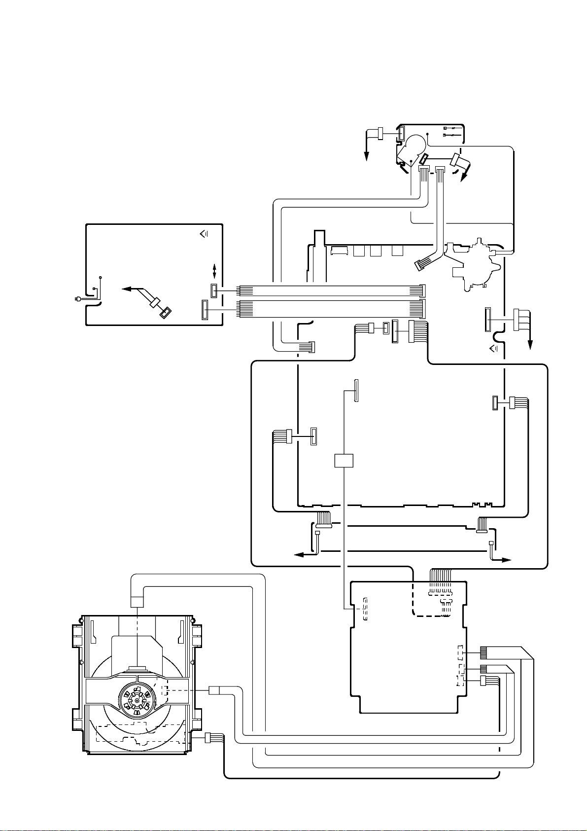
4. ELECTRICAL ADJUSTMENT PARTS LOCATION GUIDE (WIRING CONNECTION)
CRT PCB
CP805
CD805
CRT
CD802
POWER PCB
J801
CP802B
TP024
CP801
TP022
CD801
CP803B
CRT
CD803
AC IN
CRT
L3800
CP3803
CP3800
VR3800
TP3801
CP3802
SPEAKER
CD702
TU001
CP101
CP802A
CP303
CD356
AV PCB
J4203 J4202
CD402
CD8004
CP8002
CD8002
OPERATION PCB
CD8502
J4201
CP803A
CP8005
CP8001
CP402
CP8004
CD8501
FB401
CP401
CP102
CD355
VR402
CRT
CD757
SPEAKER
DECK CD
CP8502
CP2601
CP2301
CP2302
DVD PCB
CD2301
CD2601
CD2302
D-6
Page 27

MECHANICAL EXPLODED VIEW
202
202
131
202
132
124
202
206
202
202
128
127
201
115
201
112
128
209
201
201
126
PCB110
(CRT PCB ASS'Y)
209
115
117
202
130
132
PCB030
(OPERATION PCB ASS'Y)
212
114
116
113
209
111
122
108
A
101
209
I-1
Page 28

123
MECHANICAL EXPLODED VIEW
208
208
121
208
207
125
206
205
206
205
210
206
206
105
PCB130
(DVD PCB ASS'Y)
205
205
107
208
208
208
PCB020
(POWER PCB ASS'Y)
208
208
119
208
208
208
206
204
102
206
207
110
211
104
204
211
106
204
103
207
211
207
204
204
129
109
206
118
206
120
206
203
206
203
A
PCB250
(AV PCB ASS'Y)
I-2
Page 29

MECHANICAL REPLACEMENT PARTS LIST
Location No. TSB P/N Reference No. Description
101 BZ310481 A5C2012720 CABINET,FRONT ASSY
102 BZ710696 761WPA0252 COVER,PCB ASS'Y
105 BZ710697 761WPA0250 HOLDER,FFC
106 BZ710698 761WSA0093 ANGLE,DECK
107 BZ710039 8995034000 CORD CLIP UL CO.
109 BZ710699 761WPA0249 HOLDER,FBT
110 BZ710401 769WPA0018 GUIDE,CONNECTOR(FFC)
111 BZ710775 701WPJB907 CABINET,FRONT
112 BZ710660 741WUA0021 SPRING,EARTH
113 BZ710396 713WPA0147 GLASS,LED
116 BZ710404 735WPB0124 BUTTON,FRAME
117 BZ710776 702WPA0960 CABINET,BACK
118 BZ710706 702WSA0125 PLATE,BOTTOM
119 BZ710777 702WSA0144 SHIELD,TOP
120 BZ710708 7230007529 SHEET,JACK
122 BZ710778 752WSA0302 SHIELD,AV JACK
123 BZ710407 712WPB0075 PLATE,TRAY-FRONT
127 BZ710258 741WUA0001 SPRING,EARTH
128 BZ710259 762WPA0011 HOLDER,CRT WIRE
129 BZ710260 899HV3T000 HOLDER,ANODE WIRE
130 BZ310503 A5C2012740 CABINET,BACK ASSY
201 BZ710275 8121J50B54 SCREW,TAPPING(B0) GW20 5x28
202 BZ710035 8117540A64 SCREW,TAPPING(B0) TRUSS 4x16
203 BZ710320 8117540804 SCREW,TAPPING(B0) TRUSS 4x8
204 BZ710239 8109I30A04 SCREW,TAP TITE(B) WH7 3x10
205 BZ710562 8109I30804 SCREW,TAP TITE(B) WH7 3x8
206 BZ710678 8109230804 SCREW,TAP TITE(B) BIND 3x8
207 BZ710581 8109230704 SCREW,TAP TITE(B) R BIND 3x7
208 BZ710408 8109630604 SCREW,TAP TITE(B) BRAZIER 3x6
209 BZ710031 8110630A04 SCREW,TAP TITE(P) BRAZIER 3x10
210 BZ710187 8110226804 SCREW,TAP TITE(P) BIND 2.6x8
211 BZ710018 8107630804 SCREW,TAP TITE(S) BRAZIER 3x8
212 BZ710030 8110630804 SCREW,TAP TITE(P) BRAZIER 3x8
--- BZ710410 792WHA0317 PACKAGE,TOP
--- BZ710411 792WHA0318 PACKAGE,BOTTOM
--- BZ614496 J5C20101 INSTRUCTION BOOK
J1-1
Page 30

ELECTRICAL REPLACEMENT PARTS LIST
Location No. TSB P/N Reference No. Description
RESISTORS
R232 BZ210282 R00104154J RC 150K OHM 1/4W or
! R401 BZ210140 R002T2331J RC 330 OHM 1/2W
R402 BZ210284 R3X28A271J R,METAL OXIDE 270 OHM 2W
R408 BZ210285 R3X28AR47J R,METAL OXIDE 0.47 OHM 2W
! R425 BZ210140 R002T2331J RC 330 OHM 1/2W
! R442 BZ210072 R801R7223F RC 22K OHM 1/10W
! R444 BZ210263 R801R7562F RC 5.6K OHM 1/10W
! R447 BZ210021 R65582680J R,FUSE 68 OHM 1/2W
R448 BZ210153 R3X181102J R,METAL OXIDE 1K OHM 1W
R450 BZ210032 R6558A3R9J R,FUSE 3.9 OHM 2W
! R803 BZ210050 R3X18A123J R,METAL OXIDE 12K OHM 2W
! R805 BZ210050 R3X18A123J R,METAL OXIDE 12K OHM 2W
! R807 BZ210050 R3X18A123J R,METAL OXIDE 12K OHM 2W
R3011 BZ210286 R00202822J RC 8.2K OHM 1/2W or
! R3802 BZ210158 R002T2563J RC 56K OHM 1/2W
! R3803 BZ210206 R002T2155J RC 1.5M OHM 1/2W
! R3806 BZ210080 R0G3K2275K RC 2.7M OHM 1/2W
! R3812 BZ210217 R3X181331J R,METAL OXIDE 330 OHM 1W
! R3817 BZ210117 R5X2CE010J R,CEMENT 1 OHM 7W
R3821 BZ210248 R3X181R15J R,METAL OXIDE 0.15 OHM 1W
! R3828 BZ210190 R63581R22J R,FUSE 0.22 OHM 1W
R4276 BZ210288 R00204750J RC 75 OHM 1/4W or
R4284 BZ210291 R00204221J RC 220 OHM 1/4W or
BZ210283 R001T4154J RC 150K OHM 1/4W
BZ210287 R002T2822J RC 8.2K OHM 1/2W
BZ210107 R002T4750J RC 75 OHM 1/4W
BZ210135 R002T4221J RC 220 OHM 1/4W
CAPACITORS
C331 BZ110269 P1S300332J CP 0.0033UF 50V or
! C407 BZ110101 E5EZF3222M CE 2200 UF 25V
C409 BZ110259 E5EZ04101M CE 100 UF 35V or
C423 BZ110136 P4J7F3394J CMPP 0.39 UF 250V PMS
! C428 BZ110058 P4N8FJ123H CMPP 0.012 UF 1.25KV
C431 BZ110204 E0ELFD220M CE 22 UF 250V
! C433 BZ110205 E02LU5220M CE 22 UF 50V
C450 BZ110182 C03L0R713K CC 0.001 UF 2KV R
C645 BZ110260 E0EE052R2M CE 2.2 UF 50V
C649 BZ110120 E0EL054R7M CE 4.7 UF 50V
C802 BZ110247 C0JBB0713K CC 0.001 UF 2KV B
! C3801 BZ110138 P2472B224M CMP 0.22UF 275V PHE840
C3802 BZ110223 CD39E0M13M CC 0.001 UF 250V
C3803 BZ110223 CD39E0M13M CC 0.001 UF 250V
! C3804 BZ110145 P2472B104M CMP 0.1 UF 275V PHE840
! C3810 BZ110247 C0JBB0713K CC 0.001 UF 2KV B
C3811 BZ110191 C03L0R7E3K CC 0.0015UF 2KV R
! C3812 BZ110247 C0JBB0713K CC 0.001 UF 2KV B
! C3815 BZ110012 E51CGC471M CE 470 UF 200V
! C3816 BZ110222 CD39E0MH3M CC 0.0022UF 250V
! C3820 BZ110261 E5EZU8100M CE 10 UF 100V
! C3822 BZ110129 E5EZF2222M CE 2200 UF 16V
! C3823 BZ110032 E5EZF3102M CE 1000 UF 25V
C3824 BZ110219 C0PLRR7Q2K CC 470 PF 2KV RR
! C3826 BZ110130 E62NFC221M CE 220 UF 200V
C3827 BZ110129 E5EZF2222M CE 2200 UF 16V
C4276 BZ110262 E02L05100M CE 10 UF 50V or
C4277 BZ110262 E02L05100M CE 10 UF 50V or
C4278 BZ110271 CHG0B04K2J CC 270 PF 50V B or
C4279 BZ110273 CHG0CH4H1J CC 22 PF 50V CH or
C4280 BZ110275 CHG0B04H2J CC 220 PF 50V B or
BZ110270 CQGTB04L3K CC 0.0033UF 50V B
BZ110018 E5EZT4101M CE 100 UF 35V
BZ110106 E02LT5100M CE 10 UF 50V
BZ110106 E02LT5100M CE 10 UF 50V
BZ110272 CHGTB04K2J CC 270 PF 50V B
BZ110274 CHGTCH4H1J CC 22 PF 50V CH
BZ110276 CHGTB04H2J CC 220 PF 50V B
DIODES
D101 BZ410006 D1VT001330 DIODE,SILICON 1SS133T-77
D104 BZ410022 D97U06R81B DIODE,ZENER MTZJ6.8B T-77
D105 BZ410006 D1VT001330 DIODE,SILICON 1SS133T-77
D202 BZ410006 D1VT001330 DIODE,SILICON 1SS133T-77
D401 BZ410043 D2WT011E10 DIODE,SILICON 11E1-EIC
D403 BZ410037 D97U03301B DIODE,ZENER MTZJ33B T-77
D404 BZ410037 D97U03301B DIODE,ZENER MTZJ33B T-77
D405 BZ410006 D1VT001330 DIODE,SILICON 1SS133T-77
D406 BZ410006 D1VT001330 DIODE,SILICON 1SS133T-77
D408 BZ410037 D97U03301B DIODE,ZENER MTZJ33B T-77
J2-1
Page 31

ELECTRICAL REPLACEMENT PARTS LIST
Location No. TSB P/N Reference No. Description
DIODES
D409 BZ410006 D1VT001330 DIODE,SILICON 1SS133T-77
D410 BZ410022 D97U06R81B DIODE,ZENER MTZJ6.8B T-77
D411 BZ410092 D2WXN49370 DIODE,SILICON 1N4937
! D412 BZ410014 D2LTPG06J0 DIODE,SILICON RMPG06J-G3
D413 BZ410092 D2WXN49370 DIODE,SILICON 1N4937
D414 BZ410043 D2WT011E10 DIODE,SILICON 11E1-EIC
D415 BZ410101 D28TELS6N6 DIODE,RECTIFER 10ELS6N-TA1B2
D416 BZ410020 D97U05R11B DIODE,ZENER MTZJ5.1B T-77
D601 BZ410006 D1VT001330 DIODE,SILICON 1SS133T-77
D602 BZ410006 D1VT001330 DIODE,SILICON 1SS133T-77
D603 BZ410006 D1VT001330 DIODE,SILICON 1SS133T-77
D606 BZ410022 D97U06R81B DIODE,ZENER MTZJ6.8B T-77
D607 BZ410022 D97U06R81B DIODE,ZENER MTZJ6.8B T-77
D608 BZ410022 D97U06R81B DIODE,ZENER MTZJ6.8B T-77
D612 BZ410059 D2WT11ES10 DIODE,SILICON 11ES1-EIC
D613 BZ410006 D1VT001330 DIODE,SILICON 1SS133T-77
D614 BZ410006 D1VT001330 DIODE,SILICON 1SS133T-77
D615 BZ410006 D1VT001330 DIODE,SILICON 1SS133T-77
D752 BZ410022 D97U06R81B DIODE,ZENER MTZJ6.8B T-77
D792 BZ410087 0021E2Q140 LED LTL-1CHEE-002A
D801 BZ410006 D1VT001330 DIODE,SILICON 1SS133T-77
D802 BZ410006 D1VT001330 DIODE,SILICON 1SS133T-77
D803 BZ410006 D1VT001330 DIODE,SILICON 1SS133T-77
D1001 BZ410119 DDDRL41480 DIODE,SILICON MCL4148
D2601 BZ410120 DDARDS1210 DIODE,SILICON KDS121RTK
D2602 BZ410121 DDARDS1200 DIODE,SILICON KDS120RTK
D3000 BZ410006 D1VT001330 DIODE,SILICON 1SS133T-77
D3002 BZ410043 D2WT011E10 DIODE,SILICON 11E1-EIC
D3003 BZ410122 D97U01201B DIODE,ZENER MTZJ12B T-77
D3004 BZ410023 D97U09R11B DIODE,ZENER MTZJ9.1B T-77
D3005 BZ410006 D1VT001330 DIODE,SILICON 1SS133T-77
D3006 BZ410043 D2WT011E10 DIODE,SILICON 11E1-EIC
D3007 BZ410022 D97U06R81B DIODE,ZENER MTZJ6.8B T-77
D3801 BZ410021 D97U05R61B DIODE,ZENER MTZJ5.6B T-77
D3802 BZ410006 D1VT001330 DIODE,SILICON 1SS133T-77
D3804 BZ410100 D97U01801B DIODE,ZENER MTZJ18B T-77
D3806 BZ410006 D1VT001330 DIODE,SILICON 1SS133T-77
D3807 BZ410092 D2WXN49370 DIODE,SILICON 1N4937
! D3808 BZ410062 D2WTRM11C0 DIODE,SILICON RM11C-EIC
! D3809 BZ410062 D2WTRM11C0 DIODE,SILICON RM11C-EIC
D3810 BZ410100 D97U01801B DIODE,ZENER MTZJ18B T-77
! D3815 BZ410062 D2WTRM11C0 DIODE,SILICON RM11C-EIC
! D3816 BZ410062 D2WTRM11C0 DIODE,SILICON RM11C-EIC
! D3817 BZ410115 D2LKB340L0 DIODE,SCHOTTKY SB340L-6737
! D3818 BZ410092 D2WXN49370 DIODE,SILICON 1N4937
! D3819 BZ410010 D28T21DQN9 DIODE,SCHOTTKY 21DQ09N-TA2B1
! D3820 BZ410076 D2WXB290S0 DIODE,SILICON SB290S
! D3821 BZ410080 D2WXRU2AM0 DIODE,SILICON RU2AM-EIC
D3822 BZ410006 D1VT001330 DIODE,SILICON 1SS133T-77
! D3823 BZ410076 D2WXB290S0 DIODE,SILICON SB290S
! D3824 BZ410076 D2WXB290S0 DIODE,SILICON SB290S
D3825 BZ410084 D97U01101B DIODE,ZENER MTZJ11B T-77
D3826 BZ410006 D1VT001330 DIODE,SILICON 1SS133T-77
! D3827 BZ410006 D1VT001330 DIODE,SILICON 1SS133T-77
D3828 BZ410064 D97U03R91B DIODE,ZENER MTZJ3.9B T-77
D3829 BZ410006 D1VT001330 DIODE,SILICON 1SS133T-77
! D3830 BZ410010 D28T21DQN9 DIODE,SCHOTTKY 21DQ09N-TA2B1
D3831 BZ410020 D97U05R11B DIODE,ZENER MTZJ5.1B T-77
D4213 BZ410006 D1VT001330 DIODE,SILICON 1SS133T-77
D8504 BZ410116 DD5R002260 DIODE,SILICON 1SS226(TE85L)
D8505 BZ410116 DD5R002260 DIODE,SILICON 1SS226(TE85L)
D8506 BZ410116 DD5R002260 DIODE,SILICON 1SS226(TE85L)
ICS
IC101 BZ611140 I55D06070B IC OEC6070B
IC103 BZ611122 I9UF032450 IC PST3245NR
IC199 BZ310474 A5C2011255 IC S-24C08ADPA-01
IC301 BZ611063 I06F062420 IC M62420FP
! IC302 BZ611035 I0FSP75220 IC AN7522
! IC401 BZ611025 I03TD80400 IC LA78040
IC601 BZ611064 I05DC12530 IC TB1253N
IC602 BZ611078 I03F071510 IC LA7151M-TLM
IC902 BZ611068 I01FF58290 IC AN5829S
IC1001 BZ611123 ICQF067050 IC ZR36705
IC1006 BZ611124 I5HJ004BF0 IC S-24C04BFJ-TB
IC1501 BZ611079 I05FE90A45 IC TC90A45F
IC2001 BZ611125 I53F086610 IC LC78661W
IC2002 BZ611106 I59J0258B3 IC MSM5416258B-30
J2-2
Page 32

ELECTRICAL REPLACEMENT PARTS LIST
Location No. TSB P/N Reference No. Description
ICS
IC2301 BZ611126 I03F065600 IC LA6560
IC2601 BZ611127 I07F04066F IC BU4066BCF
IC2602 BZ611128 I03FR97020 IC LA9702WL
! IC3000 BZ611054 I1KA98R050 IC KIA78R05PI
! IC3001 BZ611089 I1KA98R09A IC KIA78R09API
! IC3002 BZ611054 I1KA98R050 IC KIA78R05PI
! IC3003 BZ611054 I1KA98R050 IC KIA78R05PI
IC3004 BZ611054 I1KA98R050 IC KIA78R05PI
! IC3800 BZ410088 0002E00610 PHOTO COUPLER LTV-817M-VB
IC4001 BZ611110 ICQF067320 IC ZR36732
IC4002 BZ611112 I59J0160FB IC MSM56V16160F-8
IC4005 BZ611129 ICMJ0800A7 IC SST39VF800A-70-4C-EK
IC4006 BZ611130 I0GF9XZ010 IC PQ070XZ01ZP
IC4201 BZ611074 I0QF045800 IC NJM4580M
IC4202 BZ611075 I5CF040530 IC CD4053BNSR
IC4203 BZ611066 I0UD013110 IC MM1311AD
IC8503 BZ611131 I17F017480 IC PCM1748E
IC8504 BZ611073 I5CF040520 IC SN74LV4052APW
TRANSISTORS
Q103 BZ510109 TCAA3875SY TRANSISTOR,SILICON KTC3875S_Y_RTK
Q104 BZ510108 TAAA1504SY TRANSISTOR,SILICON KTA1504S_Y_RTK
Q105 BZ510109 TCAA3875SY TRANSISTOR,SILICON KTC3875S_Y_RTK
Q109 BZ510109 TCAA3875SY TRANSISTOR,SILICON KTC3875S_Y_RTK
Q202 BZ510109 TCAA3875SY TRANSISTOR,SILICON KTC3875S_Y_RTK
Q203 BZ510109 TCAA3875SY TRANSISTOR,SILICON KTC3875S_Y_RTK
Q204 BZ510109 TCAA3875SY TRANSISTOR,SILICON KTC3875S_Y_RTK
Q205 BZ510114 T8AA03881S TRANSISTOR,SILICON KTC3881S-RTK
Q301 BZ510109 TCAA3875SY TRANSISTOR,SILICON KTC3875S_Y_RTK
! Q401 BZ510004 TA3T016240 TRANSISTOR,SILICON 2SA1624-AA
Q403 BZ510068 TNAAJ05003 COMPOUND TRANSISTOR KRC111SRTK
Q404 BZ510073 TAATA12660 TRANSISTOR,SILICON KTA1266-AT(Y,GR)
! Q405 BZ510097 TCAT03227Y TRANSISTOR,SILICON KTC3227_Y-AT
Q406 BZ510028 TDUF024990 TRANSISTOR,SILICON 2SD2499
Q601 BZ510109 TCAA3875SY TRANSISTOR,SILICON KTC3875S_Y_RTK
Q603 BZ510109 TCAA3875SY TRANSISTOR,SILICON KTC3875S_Y_RTK
Q608 BZ510109 TCAA3875SY TRANSISTOR,SILICON KTC3875S_Y_RTK
Q609 BZ510090 TPAAB05001 COMPOUND TRANSISTOR KRA102SRTK
Q801 BZ510080 TCYT1740S0 TRANSISTOR,SILICON 2SC1740SP TP
Q802 BZ510080 TCYT1740S0 TRANSISTOR,SILICON 2SC1740SP TP
Q803 BZ510080 TCYT1740S0 TRANSISTOR,SILICON 2SC1740SP TP
! Q804 BZ510091 TCA0042170 TRANSISTOR,SILICON KTC4217(O,Y)
! Q805 BZ510091 TCA0042170 TRANSISTOR,SILICON KTC4217(O,Y)
! Q806 BZ510091 TCA0042170 TRANSISTOR,SILICON KTC4217(O,Y)
Q1501 BZ510109 TCAA3875SY TRANSISTOR,SILICON KTC3875S_Y_RTK
Q1502 BZ510109 TCAA3875SY TRANSISTOR,SILICON KTC3875S_Y_RTK
Q1503 BZ510109 TCAA3875SY TRANSISTOR,SILICON KTC3875S_Y_RTK
Q2301 BZ510109 TCAA3875SY TRANSISTOR,SILICON KTC3875S_Y_RTK
Q2302 BZ510108 TAAA1504SY TRANSISTOR,SILICON KTA1504S_Y_RTK
Q2303 BZ510071 TNAAB05003 COMPOUND TRANSISTOR KRC102SRTK
Q2304 BZ510108 TAAA1504SY TRANSISTOR,SILICON KTA1504S_Y_RTK
Q2601 BZ510109 TCAA3875SY TRANSISTOR,SILICON KTC3875S_Y_RTK
Q2603 BZ510112 T67J1036K0 TRANSISTOR,SILICON 2SA1036KT146
Q2604 BZ510112 T67J1036K0 TRANSISTOR,SILICON 2SA1036KT146
Q2605 BZ510108 TAAA1504SY TRANSISTOR,SILICON KTA1504S_Y_RTK
Q2606 BZ510109 TCAA3875SY TRANSISTOR,SILICON KTC3875S_Y_RTK
Q2607 BZ510113 T27T030180 FET 2SK3018
Q2608 BZ510109 TCAA3875SY TRANSISTOR,SILICON KTC3875S_Y_RTK
Q2609 BZ510109 TCAA3875SY TRANSISTOR,SILICON KTC3875S_Y_RTK
Q2610 BZ510109 TCAA3875SY TRANSISTOR,SILICON KTC3875S_Y_RTK
Q2611 BZ510108 TAAA1504SY TRANSISTOR,SILICON KTA1504S_Y_RTK
Q2612 BZ510113 T27T030180 FET 2SK3018
Q2613 BZ510113 T27T030180 FET 2SK3018
Q2614 BZ510109 TCAA3875SY TRANSISTOR,SILICON KTC3875S_Y_RTK
Q2615 BZ510109 TCAA3875SY TRANSISTOR,SILICON KTC3875S_Y_RTK
Q2616 BZ510109 TCAA3875SY TRANSISTOR,SILICON KTC3875S_Y_RTK
Q3000 BZ510060 TB3T011310 TRANSISTOR,SILICON 2SB1131(S,T)-AE
Q3001 BZ510071 TNAAB05003 COMPOUND TRANSISTOR KRC102SRTK
Q3002 BZ510109 TCAA3875SY TRANSISTOR,SILICON KTC3875S_Y_RTK
! Q3003 BZ510076 TB30011430 TRANSISTOR,SILICON 2SB1143(S,T,U)
Q3004 BZ510109 TCAA3875SY TRANSISTOR,SILICON KTC3875S_Y_RTK
Q3005 BZ510105 TCAT03209Y TRANSISTOR,SILICON KTC3209_Y-AT
Q3800 BZ510069 TCATC31980 TRANSISTOR,SILICON KTC3198-AT(Y,GR)
Q3801 BZ510069 TCATC31980 TRANSISTOR,SILICON KTC3198-AT(Y,GR)
Q3802 BZ510070 TCAT032034 TRANSISTOR,SILICON KTC3203_Y-AT
Q3803 BZ510098 T220033260 FET 2SK3326(2)
Q4201 BZ510109 TCAA3875SY TRANSISTOR,SILICON KTC3875S_Y_RTK
Q4202 BZ510108 TAAA1504SY TRANSISTOR,SILICON KTA1504S_Y_RTK
J2-3
Page 33

ELECTRICAL REPLACEMENT PARTS LIST
Location No. TSB P/N Reference No. Description
TRANSISTORS
Q4203 BZ510088 TNAAD05001 COMPOUND TRANSISTOR KRC104SRTK
Q4204 BZ510109 TCAA3875SY TRANSISTOR,SILICON KTC3875S_Y_RTK
Q4205 BZ510090 TPAAB05001 COMPOUND TRANSISTOR KRA102SRTK
Q4206 BZ510109 TCAA3875SY TRANSISTOR,SILICON KTC3875S_Y_RTK
Q4207 BZ510109 TCAA3875SY TRANSISTOR,SILICON KTC3875S_Y_RTK
Q4208 BZ510109 TCAA3875SY TRANSISTOR,SILICON KTC3875S_Y_RTK
Q4209 BZ510067 TNAAC05002 COMPOUND TRANSISTOR KRC103SRTK
Q4210 BZ510107 TPAAA05001 COMPOUND TRANSISTOR KRA101SRTK
Q4211 BZ510109 TCAA3875SY TRANSISTOR,SILICON KTC3875S_Y_RTK
Q4212 BZ510109 TCAA3875SY TRANSISTOR,SILICON KTC3875S_Y_RTK
Q4213 BZ510067 TNAAC05002 COMPOUND TRANSISTOR KRC103SRTK
Q4214 BZ510109 TCAA3875SY TRANSISTOR,SILICON KTC3875S_Y_RTK
Q4215 BZ510108 TAAA1504SY TRANSISTOR,SILICON KTA1504S_Y_RTK
Q4217 BZ510088 TNAAD05001 COMPOUND TRANSISTOR KRC104SRTK
Q752A BZ510079 TNATX05001 COMPOUND TRANSISTOR KRC114MAT
Q8502 BZ510108 TAAA1504SY TRANSISTOR,SILICON KTA1504S_Y_RTK
Q8503 BZ510108 TAAA1504SY TRANSISTOR,SILICON KTA1504S_Y_RTK
Q8504 BZ510108 TAAA1504SY TRANSISTOR,SILICON KTA1504S_Y_RTK
Q8506 BZ510102 TS5M000037 COMPOUND TRANSISTOR HN1C03F_B(TE85L)
COILS &TRANSFORMERS
L001 BZ310041 02167F101J COIL 100 UH
L201 BZ310067 021LA6180K COIL 18 UH
L202 BZ310041 02167F101J COIL 100 UH
L203 BZ310041 02167F101J COIL 100 UH
L204 BZ310049 021LA6R22M COIL 0.22 UH
L205 BZ310038 021LA6120K COIL 12 UH
L207 BZ310136 021LA63R3K COIL 3.3 UH
L302 BZ310041 02167F101J COIL 100 UH
L303 BZ310041 02167F101J COIL 100 UH
L401 BZ310004 021679472K COIL 4.7 MH
L402 BZ310063 022100027A COIL,LINEARITY ELH5L4113
L602 BZ310041 02167F101J COIL 100 UH
L603 BZ310204 02167D221K COIL 220 UH
L605 BZ613032 10380R1501 DELAY EQ 380R1501
L606 BZ310042 021LA6101K COIL 100 UH
L801 BZ310170 021673151K COIL 150 UH
L802 BZ310170 021673151K COIL 150 UH
L803 BZ310170 021673151K COIL 150 UH
L804 BZ310170 021673151K COIL 150 UH
L902 BZ310041 02167F101J COIL 100 UH
L1001 BZ310191 02167F2R2J COIL 2.2 UH
L1501 BZ310140 02167F150J COIL 15 UH
L1502 BZ310140 02167F150J COIL 15 UH
L1503 BZ310138 021673821K COIL 820 UH
L1504 BZ310139 02167F151J COIL 150 UH
! L3800 BZ310066 028R200024 COIL,DEGAUSS 8R200024
! L3801 BZ310180 029T000105 COIL,LINE FILTER 2R2A752F28
L3803 BZ310181 02A6B2E0A1 CORE,FERRITE HF70T22*10*14
L4201 BZ310133 02167D472K COIL 4.7 MH
L4202 BZ310002 021673101K COIL 100 UH
L4203 BZ310041 02167F101J COIL 100 UH
L4204 BZ310041 02167F101J COIL 100 UH
L4205 BZ310041 02167F101J COIL 100 UH
L4206 BZ310209 021L961R0M COIL 1 UH or
L8502 BZ310192 0216S71R8J COIL 1.8 UH
L8503 BZ310192 0216S71R8J COIL 1.8 UH
L8504 BZ310192 0216S71R8J COIL 1.8 UH
L8505 BZ310140 02167F150J COIL 15 UH
L8507 BZ310118 02AHB9A972 CORE,FERRITE W5T29X7.5X19
T401 BZ310172 045013003J TRANS,HORIZONTAL DRIVE ETH14Y47AY
! T3800 BZ310205 0481350824 TRANSFORMER,SWITCHING 81350824
BZ310077 021LA61R0M COIL 1 UH
JACKS
! J351 BZ614002 060G131014 RCA JACK HTJ-035-28A
J701 BZ614114 0602431013 RCA JACK JPJ1187-010010
! J801 BZ614115 066C130017 SOCKET,CATHODE RAY TUBE CVT3275-5101
J4201 BZ614400 060J401082 RCA JACK MSP-251V-05PBSN
J4202 BZ614399 060J411018 RCA JACK MSP-213V1-432 PBSN
J4203 BZ614398 060J431019 RCA JACK MSP-213V2-432 PBSN
SWITCHES
SW751 BZ612010 0504101T34 SWITCH,TACT EVQ21505R
SW791 BZ612010 0504101T34 SWITCH,TACT EVQ21505R
SW792 BZ612010 0504101T34 SWITCH,TACT EVQ21505R
SW793 BZ612010 0504101T34 SWITCH,TACT EVQ21505R
SW794 BZ612010 0504101T34 SWITCH,TACT EVQ21505R
SW795 BZ612010 0504101T34 SWITCH,TACT EVQ21505R
SW796 BZ612010 0504101T34 SWITCH,TACT EVQ21505R
J2-4
Page 34

ELECTRICAL REPLACEMENT PARTS LIST
Location No. TSB P/N Reference No. Description
SWITCHES
SW797 BZ612010 0504101T34 SWITCH,TACT EVQ21505R
SW798 BZ612010 0504101T34 SWITCH,TACT EVQ21505R
SW799 BZ612010 0504101T34 SWITCH,TACT EVQ21505R
VARIABLE RESISTORS
VR402 BZ210238 V1K6313BTE VOLUME,SEMI FIXED NVG6TLTAB102
VR3800 BZ210265 V1K63Q2BTE VOLUME,SEMI FIXED NVG6TLTAB471
P.C.BOARD ASSEMBLIES
PCB020 BZ310475 A5C2012020 PCB ASS'Y VPB157A
PCB030 BZ310476 A5C2012030 PCB ASS'Y TEXA33C
PCB110 BZ310477 A5C2012110 PCB ASS'Y TCB402A
PCB130 BZ310478 A5C2012130 PCB ASS'Y VMB261A
PCB250 BZ310479 A5C2012250 PCB ASS'Y TMB543A
MISCELLANEOUS
B301 BZ310129 024HT03564 CORE,BEADS W4BRH3.5X6X1
B1001 BZ310186 024HC31022 CORE,BEADS FCM2012H-102T04
B1002 BZ310186 024HC31022 CORE,BEADS FCM2012H-102T04
B2001 BZ310186 024HC31022 CORE,BEADS FCM2012H-102T04
B2002 BZ310186 024HC31022 CORE,BEADS FCM2012H-102T04
B2003 BZ310186 024HC31022 CORE,BEADS FCM2012H-102T04
B2601 BZ310186 024HC31022 CORE,BEADS FCM2012H-102T04
B2602 BZ310186 024HC31022 CORE,BEADS FCM2012H-102T04
B2604 BZ310186 024HC31022 CORE,BEADS FCM2012H-102T04
B2605 BZ310186 024HC31022 CORE,BEADS FCM2012H-102T04
B2606 BZ310186 024HC31022 CORE,BEADS FCM2012H-102T04
B3800 BZ310122 024HT03563 CORE,BEADS W4BRH3.5X6X1.0X2
B3801 BZ310121 024HT03553 CORE,BEADS W5RH3.5X5X1.0
B4001 BZ310186 024HC31022 CORE,BEADS FCM2012H-102T04
B4002 BZ310186 024HC31022 CORE,BEADS FCM2012H-102T04
B4003 BZ310186 024HC31022 CORE,BEADS FCM2012H-102T04
B4004 BZ310186 024HC31022 CORE,BEADS FCM2012H-102T04
B4201 BZ310129 024HT03564 CORE,BEADS W4BRH3.5X6X1
B8501 BZ310186 024HC31022 CORE,BEADS FCM2012H-102T04
B8502 BZ310186 024HC31022 CORE,BEADS FCM2012H-102T04
BL001 BZ310014 023C00022A COIL BALUN HPN-01
CD355 BZ614226 06CU123802 CORD,CONNECTOR CU123802
CD356 BZ614226 06CU123802 CORD,CONNECTOR CU123802
CD402 BZ614445 WDL6016038 FLAT CABLE AWM2468 AWG26 6C BLACK 160MM
CD702 BZ614206 06CU2B2801 CORD,CONNECTOR CU2B2801
CD757 BZ614231 06CU292501 CORD,CONNECTOR CU292501
CD801 BZ614378 06CU823001 CORD,CONNECTOR CU823001
CD802 BZ614492 WCL6850038 FLAT CABLE AWM2468 AWG26 5C GRAY 500MM
CD803 BZ614493 WBL6032038 FLAT CABEL AWM2468 AWG26 4C BLACK 320MM
CD805 BZ614378 06CU823001 CORD,CONNECTOR CU823001
CF201 BZ613016 1011T4R517 FILTER,CERAMIC EFCT4R5MW5
CF202 BZ613015 1011T4R504 FILTER,CERAMIC EFCT4R5YS5A
CF203 BZ613031 1029045R7G FILTER,SAW TSF5229P3
CF204 BZ613018 1012T04702 FILTER,CERAMIC TRAP MKT47.3MC110P-TF
CP101 BZ614380 069X170379 CONNECTOR PCB SIDE 07JQ-ST
CP102 BZ614239 069S290639 CONNECTOR PCB SIDE A2001WR2-9P
CP303 BZ614214 069S2B0629 CONNECTOR PCB SIDE A2001WV2-11P
! CP401 BZ614303 069S450089 CONNECTOR PCB SIDE A1561WV2-A5P
CP402 BZ614333 067U006049 WIRE HOLDER B2013H02-6P
CP801 BZ614269 069S320010 CONNECTOR PCB SIDE A2361WV2-2P
CP805 BZ614269 069S320010 CONNECTOR PCB SIDE A2361WV2-2P
CD2301 BZ614435 122H081007 CORD,JUMPER 2H081007
CD2302 BZ614436 06CU251002 CORD,CONNECTOR CU251002
CD2601 BZ614437 122H0O2102 CORD,JUMPER 2H0O2102
! CD3800 BZ614341 120R414903 CORD,AC BUSH 0R414903
CD8002 BZ614438 122H0I0102 CORD,JUMPER 2H0I0102
CD8004 BZ614448 WHL6016038 FLAT CABLE AWM2468 AWG26 10C BLACK 160MM
CD8501 BZ614414 06CU2D3001 CORD,CONNECTOR CU2D3001
CD8502 BZ614415 06CU262501 CORD,CONNECTOR CU262501
CP2301 BZ614439 069EV83020 CONNECTOR PCB SIDE 00_6232_008_102_800
CP2302 BZ614440 069S250639 CONNECTOR PCB SIDE A2001WR2-5P
CP2601 BZ614494 069XYOT059 CONNECTOR PCB SIDE 24FLZ-RSM1-TB
! CP3800 BZ614283 069S420110 CONNECTOR PCB SIDE A1561WV2-2P
CP3802 BZ614366 069R260589 CONNECTOR PCB SIDE 52147-0610
CP3803 BZ614274 069R2A0589 CONNECTOR PCB SIDE 52147-1010
CP8001 BZ614420 069S2D0629 CONNECTOR PCB SIDE A2001WV2-13P
CP8002 BZ614247 069J7I0029 CONNECTOR PCB SIDE IMSA-9604S-18Z14
CP8004 BZ614273 067U010049 WIRE HOLDER B2013H02-10P
CP8005 BZ614242 069S260629 CONNECTOR PCB SIDE A2001WV2-6P
CP802A BZ614276 067U005049 WIRE HOLDER B2013H02-5P
CP802B BZ614276 067U005049 WIRE HOLDER B2013H02-5P
CP803A BZ614334 067U004029 WIRE HOLDER B2013H02-4P
CP803B BZ614334 067U004029 WIRE HOLDER B2013H02-4P
CP8502 BZ614247 069J7I0029 CONNECTOR PCB SIDE IMSA-9604S-18Z14
J2-5
Page 35

ELECTRICAL REPLACEMENT PARTS LIST
Location No. TSB P/N Reference No. Description
MISCELLANEOUS
CUS031 BZ710279 800WFAA006 CUSHION A
CUS251 BZ710279 800WFAA006 CUSHION A
CUS252 BZ710149 800WFAA008 CUSHION C
! DK4001 BZ310397 169G00014A DECK CD DVD-KDR717SK
EL001 BZ614044 124120301A EYE LET XRY20X30BD
EL002 BZ614043 124116281A EYE LET XRY16X28BD
EL003 BZ614044 124120301A EYE LET XRY20X30BD
EL004 BZ614043 124116281A EYE LET XRY16X28BD
! F3800 BZ614177 081PC05004 FUSE 51MS050LCC
FB401 BZ310206 043220056F TRANSFORMER,FLYBACK 3220056F
FH3800 BZ614005 06710T0006 HOLDER,FUSE EYF-52BC
FH3801 BZ614005 06710T0006 HOLDER,FUSE EYF-52BC
OS753 BZ614127 077Q000019 REMOTE RECEIVER PIC-28143TC5
PH3800 BZ614444 069D01001A CONNECTOR PCB SIDE 003P-2100
! RY3800 BZ612009 0560V20115 RELAY ALKS321
! SP351 BZ614381 070C546004 SPEAKER SG04H02BRA
! SP352 BZ614381 070C546004 SPEAKER SG04H02BRA
TM101 BZ614429 076D0EF010 TRANSMITTER TOT201N09080
! TU001 BZ310341 0145K00056 TUNER,VHF-UHF TECC1040PG32E
! TH3800 BZ410079 DF5EL3R0A0 DEGAUSS ELEMENT ZPB45BL3R0A
! V801 BZ614495 0981210441 CRT W/DY A51LXR195X80
X101 BZ613019 1002T01606 CERAMIC OSCILLATOR CSTLS16M0X53-A0
X601 BZ613004 100CT3R505 CRYSTAL
X1001 BZ613020 100CT01210 CRYSTAL HC-49/U
X2001 BZ613038 100CT01604 CRYSTAL HC-49/U-S
X4001 BZ613035 100WT02706 CRYSTAL HC-49/U-S
RESISTOR
CAPACITORS
RC................... CARBON RESISTOR
CC................... CERAMIC CAPACITOR
CE................... ALUMI ELECTROLYTIC CAPACITOR
CP................... POLYESTER CAPACITOR
CPP.................. POLYPROPYLENE CAPACITOR
CPL.................. PLASTIC CAPACITOR
CMP...................... METAL POLYESTER CAPACITOR
CMPL................ METAL PLASTIC CAPACITOR
CMPP................ METAL POLYPROPYLENE CAPACITOR
J2-6
Page 36

TV BLOCK DIAGRAM
CH UP
CH DOWN
VOL UP
VOL DOWN
RESET
IC103 PST3245NR
AT+5.6V
2
1
*A
FROM DVD BLOCK
POWER
ON/OFF
REC/OTR
STOP EJECT
PLAY
FF/CUE
REW
X101
16MHz
18
17
31
32
MICON
IC101
OEC6070B
5
38 37
4
19
33
22
23
24
26
27
36
MEMORY
IC199
S-24C08ADPA-01
5 6
Q105
V-BUFFER
Q103
H.BUFFER
TU001
SCL
SDA
54
AGC
1
IF
11
Q205
PRE AMP
SAW FILTER
1
4
3
CF203
*B *D
DVD C
DVD Y
DVD_A_OUT_L
DVD_A_OUT_R
ZERO
SYS MUTE
DVD_VIDEO
3
IC4201
NJM4580M
5
Q4203
MUTE DET
Q4217
MUTE SW
AMP
*G
1
7
R
Q4207
MUTE
L
Q4209, Q4210,
Q4211, Q4212
MUTE SW
LR
Q4208
13
12 5 3
AUDIO SW
MUTE
LR
14 19 18
SOUND
DECORDER
IC902
AN5829S
22 21
Q204
BUFFER
Q202, Q203
BUFFER
AV SW
*D
IC4203
MM1311AD
31
32
30
2
4
1
7
8
10
13
15
14
25
18
17
24
23
*B
10
1
VIDEO SW
4
7
LA7151M-TLM
6
5
IC602
8
3
9
19
DEGITAL SOUND
2
CONTROL
M62420FP
10
IC301
*D
Q604
X601
3.579545MHz
Q301
MUTE
14
7
20
21
22
51
6
7
9
14
15
55
42
45
16
33
38
25
24
34
10
VIF/SIF/CHROMA
IC601 TB1253N
31
9
SOUND AMP
6
8
R.OUT
G.OUT
B.OUT
Q109
Q405
IC302
AN7522
BUFFER
H.DRIVE
2
4
12
10
Q406
V.OUT
1
IC401
LA78040
H.OUT
V801
CRT
DY
3
FB401
1
9
F
FBT
S
HV
SPEAKER
SP352
SPEAKER
SP351
IC4202
CD4053BNSR
14
4
2
J701
4
6
7
E-1 E-2
*E *F
5
J4202
3
2
L
RV
6
J4203
2
RV
4
L
Q4206
BUFFER
Q1503
BUFFER
*B *D
15
DIGITAL COMB
4
FILTER
IC1501
TC90A45F
13
*D
SOUND+B
HEADPHONE
J2201
*A---AT+5.6V
*B---P.CON+9V
*C---CHROMA+5V
*D---P.CON+5V
*E---AT-80
*F---AT+80
*G---P.CON+12V
Page 37

DVD FRONT/BACK END BLOCK DIAGRAM
MECHA
Pickup
Loading
Motor
Spindle
Motor
CD/DVD
A, B, C, D, E, F
T+/–
F+/–
CHANNEL
LA9702WL
LD_DVD
LD_CD
OPEN/CLOSE
MLD1
MLD2
Motor Driver
IC2301
LA6560
SLD1/2
SP1+/–
SP_FG
D
READ
RFN/P
TE/FE
IC2602
TOST/ FOST/ BOOT3 T/T
BAL/ F BAL/ETC
SPD/SLD/TD/FD/
SPD_FG
A
E
FRONT
MD/MA_DATA
EEPROM
IC1006
S-24C04BFJ
DRAM
IC2002
EDO
DSP
IC2001
LC78661W
WR, RD,
RDY,
DVD RST
X1001
12.5MHz
SDA
SCL
C, F, D
SYSCON
IC1001
ZR36705
C
DVD/
CD
DATA
F
MA/MD_
DATA
HA/HD_DATA
E, B
REMIN
S-DRAM
IC4002
16M
MA/MD_
DATA
MPEG
IC4001
ZR36732(Vaddis 4)
SPDIF/DVD
FLASH IC
(SST)
IC4005
8M FLASH
BACK
1.9V REG
IC4006
PQ070XZ01ZP
F
ASDATAO
ABCLK
AMCLK
ALRCLK
HA/HD_DATA
F
C
X4001
27MHz
SPDIF/DVD
F
STEREO DAC
IC8503
PCM1748E
DIGITAL
AUDIO
IC8504
SN74LV4052APW
TV BLOCK
Y
C
CVBS
AUDIO L
AUDIO R
B
SPDIF-134
DVD RESET
SYS_MUTE
A P.CON+9V
B AT+D5V
C P.CON+D5V
D P.CON+A5V
E AT+D3.3V_M
F AT+3.3V
G -20V
H P.CON+D3.3VA (AT)
E-3 E-4
Page 38

L3800
DEGAUSS COIL
POWER BLOCK DIAGRAM
5V REG.
IC3002 KIA78R05PI
1
2
5V REG.
IC3004 KIA78R05PI
21
Q3002, Q3003,
Q3004
P.CON+3.3V
OUT
P.CON+3.3V
P.CON+D5V
AT+5V
AC IN
VR3800
+B ADJ.
Q3800
FEED BACK
CONTROL
F3800
IC3800
LTV-817M-VB
FEED BACK
Q3803
POWER
D3808, D3809,
D3815, D3816
RECTIFIER
TRANSFORMER
SWITCHING
T3800
8
5
10
16
15
12
5V REG.
IC3000 KIA78R05PI
21
9
5V REG.
IC3003
KIA78R05PI
2
1
9V REG.
IC3001
KIA78R09API
2
1
P.CON+5V
P.CON+5V
P.CON+5V
P.CON+9V
Q3005
DRIVE
P.CON+9V
Q3000
DRIVE
Q3001
SW
POWER ON-H
+B
FB401
4
2
E-5 E-6
Page 39
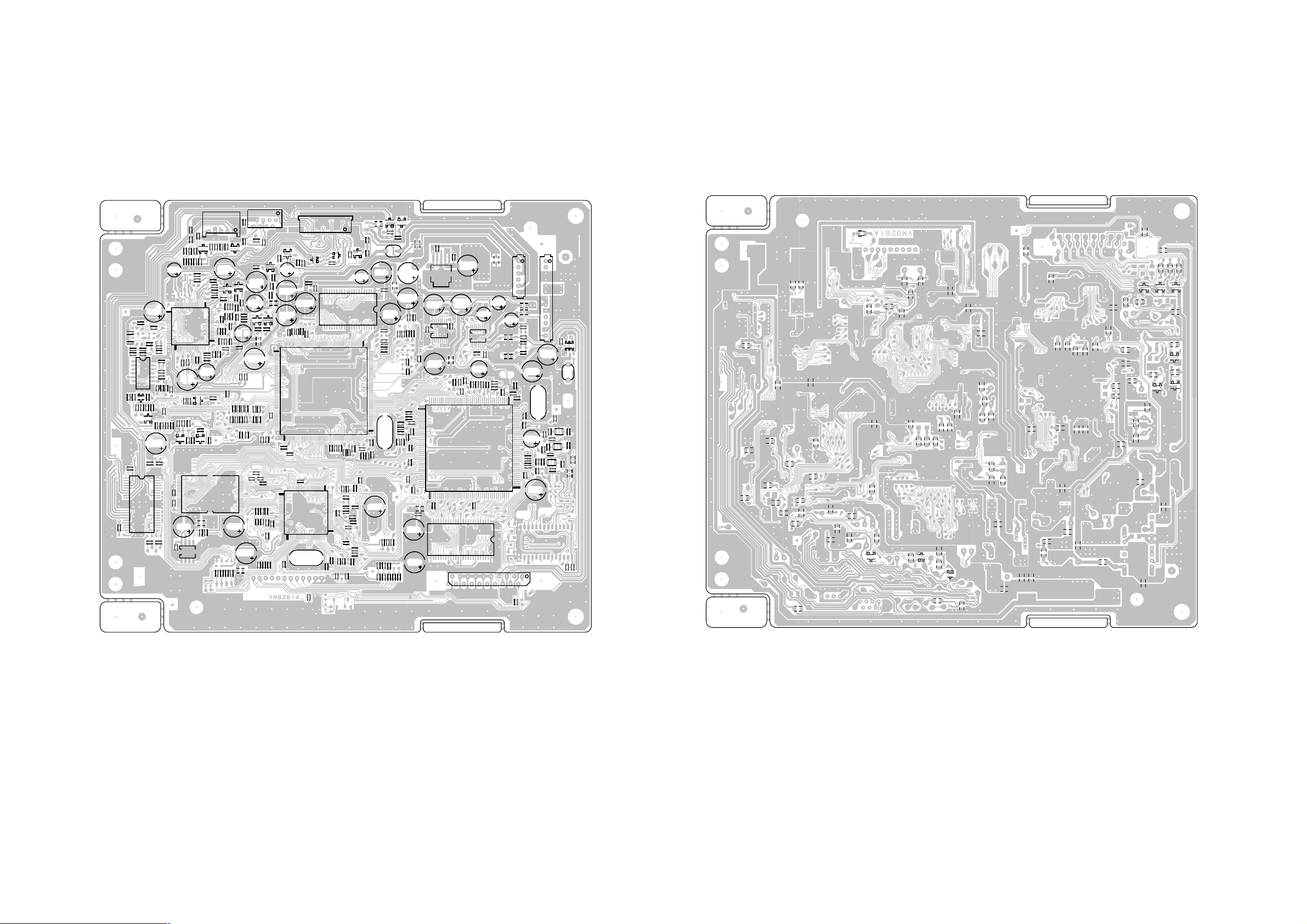
PRINTED CIRCUIT BOARDS
R2308
DVD (TOP SIDE)
C2306
R2644
R2306
C2616
C2619
W815
R1020
Q2301
R2623
R2628
R2638
R2640
C2003
C1012_1
R1034
Q2614
R2006
C2648
B1001
R2667
R2620
C2017
C2006
R2634
C2652
R2007
C2613
C2615
R2008
C2011
R2013
C1007
R1074
R2321
C2601_1
C2654
C2010
C2018
R2009
C2014
R2014
R2302
C2658
R2604
R1047
Q2606
C2015
R2010
CP2301
B2602
R1073
R1039
R1072
R1001
R2011
C2016
R2016
R1048
R1071
R1002
Q2601C2605
R1046
R2675
R2017
R1021
C2303
R1030
B2604
R1050
R2605
R1051
R2673
C1015
R2012
C2610
R2674
C2051
53
R1014
Q2604
C2612
C2045
1
CP2601
Q2603
D2601
C2609
D2602
R2610
R2611
R2671Q2615
C2611
IC2002
157
IC2001
R2020
R2021
R2022
C2048
C2033
R2023
C2041
R2024
105
R2031
R2028
R1019
W810
R2025
R2026
R2027
R2029
R2030
R1069
R1067
R1010
R1055
R1009
R1036
C1020
R1054
R1011
R1012
R1032
R1018
C1005
C1008
R1037
R1041
R1068
W828
R1038
R1066
R1031
26
1
C2021
R2064
C1009
51
IC1001
76
X1001
CP2302
C2305
C2304
R2323
C2307
R2304
C2308
Q2304
R2311
R2309
R2303R2305
R2322
R2301
R2312
C2636
R2664
R2653
R2656
R2606
R2607
C2643
C2651
R2665
Q2611
B4003
R1004
C2655
Q2608
R2642
R2631
R2643
C2641
R2651
C2602_1
R2650
Q2605
R2621
1
R2627
R2630
C2627
61
C2634
R2652
C2637
R2657
R2663
R2668
IC4005
R1005
R1016
R1015
C2620
C2618
21
R2629
R2632
W814
C2633
R2615
C2621
R2626
C2656
R2622
IC2601
Q2607
C2640
R2660
R2666
C2645
R2661
R2658
Q2610
R2318
C2310
IC2301
R2316
C2309
R2315
C2631
C2649
R2614
C2639
R2310
R2625
C2647
R2654
R2320
R2639
R2313
C2646
C2622
R2317
C4040
R4030
R2319
C1001
41
Q2609
R2649
C4045
R2647
C2642
IC2602
C2635_1
R2655
R2659
IC1006
R1070
R2609
C2032
C1004
R2608
B2601
C2037
R2033
C2023
R2035
C2034
R1024
C1021
C2024
R2036
C2043
R2307
R1049
C1011
Q2302
X2001
R1053
C2053
R1040
L1001
R1023
R4001
R4002
C1019
Q2303
R2324
B2003
R4029
C2050
B2001
C2046
C8534
R2045
R2044
IC8504
C8535
C2036
C2035
R2042
R2043
R2037
R2052
C4017
C2038
1
R4003
R4004
R4023
R4024
C4002
C4003
C4004
R4025
R4026
C4005
C4006
41 81
C4007
B4002
C4019
C4020
R1017
C4023
R1026
R1027
IC4006
C4008
C4044
B4001
R8520
R4010
C4043
IC4002
R4011
C4034
IC4001
C4041
R4017
IC8503
C8538
C4025_1
R4015
R4019
R4005
C8503
R4016
CP8502
C8506
R4018
C4026
W837
C8537
B2002
C8530
C8529
121
C4039
C8536
R8523
C4022
C1017
R2645
R2646
R2633
C2315
C2625
R2662
R2618
C1016
C2301
C2626
C2650
C2644
W839
B2605
C2623
R2603
R2670
C2608
C2659
CD8502
CD8501
B8502
B8501
R8522
W822
W821
C8526
C4037
W818
C4024
R4008
C4029_1
C4028
C4027
C4030
C4032
W811
C8523
X4001
R8502
R8501
C8525
R8504
C8502
R8503
L8502
C8508
C8509
C8505
C8504
C8510
R4007
L8504
L8503
R8516
C8512
Q8506
L8505
W802
C8513
C8514
W841
R2314
C2617
C8518
C2629
C8524
DVD (BOTTOM SIDE)
D1001
C1003
C1002
R2002
R2001
B2606
C2019
C2614
R2669
R2038
C1014
R2039
Q2612
Q2616
R1008
R2619
C2009
R2617
R1003
C1013
W808
C2020
R2672
Q2613
C2030
C2653
C1006
B1002
C2040
R2046
R2041
C2039
C2049
C2031
C2052
C1018
R2054
W831
W827
C4018
W803
W834
C4016
C4009
C4010
C4015
C4011
C4014
C4035
C4036
R4012
C4001
W838
C4038
R4027
R4028
C2002
W842
W836
C4033
R4009
W806
R4006
W829
B4004
C4031
R4021
C4012
W832
W840
R8515
W830
D8505 D8506
D8504
W804
W801
C8520
R8506
Q8502
R8507
R8508
Q8503
Q8504
C4013
W833
W835
F-1
F-2
Page 40

PRINTED CIRCUIT BOARDS
AV/CRT (INSERTED PARTS)
SOLDER SIDE
W273
W258
W019
W046
W281
W277
W071
W084
W107
W048
W049
W021
W108
C932
W100
C101
S901X
W040
W043
W030
C936
C907
W110
W111
W063
W064
S803Y
W282
W032
W029
C931
W004
W003
W061
W102
W031
D101
W274
W867
C103
W027
W036
C928
W062
W026
W865
W037
W201
R190
W083
W082
L303
W247
W845
W024
L902
C925
W079
W106
C926
W076
W058
W065
C327
S902Y
S901YS902X
W075
W066
C319
C320
R909
C921
W035
W074
IC101
W060
W067
CP303
R908
X101
D104
W199
R319
W073
W023
R318
C325
W072
IC199
W101
W103
W840
W094
W099
HS301
W093
W068
C309_1
C302_1
W092
W091
W806
C119
W844
IC302
R161
W069
W105
L1504
W089
W059
W009
W847
C308
W090
L1503
C303
L302
W206
W213
W077
W104
W212
W200
W249
W078
R4220
R4253
L4205
C4264
R4252
C4234
C1516
W051
W056
W085
W087
W053
W005
W088
W096
C4267
R4251
W256
W175
CP102
W095
W006
C4203
W174
C312
W057
C4255
W007
W097
C1518
W055
W008
W098
C4231
L4201
R805
D803
W054
R4276
C4232
W205
B301
R803
Q802
C313
W250
W052
R807
Q804Q806
L801
IC4203
C4262
D3007
C4230
C4217
S805Y
L804_1
TP024
TP022
R802
TP023
Q805
Q801 Q803
CP803B
R4257
R4259
C4227
C4261
W263
S803X
W255
C4229
W872
W164
L1501
R414_1
R418
L803_1
R806
D802D801
W211
C4269
L1502
C407
L802_1
CP8002
S106Y
C4214
C644
C645_2
R415
C
P
W001
C4268
W197
C1521_1
R416
8
0
1
W133
CP802B
W002
C4244
W196
C4207
W268
C405
C802
L605
HS401
C4228
C4256
W198
W262
C4206
R413
W235
D401
R411
W080
L4206
W894
W251
W237
W278
C4280_1
W855
C3026
R3011_1
W163
C641
W219
IC401
J801_2
W132
D3000
W210
L606
D608
D607
D606
W170
R407
W242
R421
C4279
W149
C406
W165
D614
W819
W211
W168
D601
W843
W234
W194
D613
R804
R3003
W848
W859
D615
C404_1
W162
W182
W169
W145
W146
W147
W166
R464
R463
R623
D602
D603
VR402
R417
D404
S805X
W265
W236
W240
W128
W181
C639_1
W142
W167
C421
C411
W246
D403
L402
CP805
R424
R460
T401_1
W160
W161
Q3003
C3022
C3019
C3025
W227
W238
W239
W830
CC002
C3014
W230
W231
W229
W232
W188
W189
CC001
W118
C625
W901
R624
C634
W121
C630
R632
L602
W871
W135
R629
R631
CP802A
W134
C614
D612 CF204
W259
W187
R601
W143
C649
W841
W245
C3013
D3005
C607_1
C620
R630
W261
S105Y
C621
C609
L603_1
W139
C450
W809
Q405_1
D3006
D3004
W186
C429_1
R419
R448
Q3000
IC3004
CP8001
CP8005
R215
IC601
W122
W193
C428_3
C418
W864
W252
W138
R216
C608
C618
X601
C602
W185
W192
W267
D411
W207
W257
Q3005
W190
C221
R221
W823
Q406_1
C417_1
R3012
W861
C3028
L203
C219
CF203_1
C402
HS402
R456
IC3003
W117
C213
CP401
C423
D406
R425
R401
CP8004
D3002
C3015
W216
W818
C210
D415
R447
W815
D405
S105X
HS3000
C209
C207
L207
L401
R3005
W217
IC3000
L205
W120
R
402
W225
C227
L201
W266
W224
C3011
L204
C422
C401_1
R405
S104X
C3012
D202
L202
CF201
CF202
C205
R404
W223
W220
W180
R231
S104Y
W127
W129
R406
CP402
C409
D408
IC3001
C3018
HS3001
W124
L001
W137
C3016
D3003
W125
R410
R408
W179
Q401
S106X
C001
W218
IC3002
W150
C4251
W191
W153
C4213
TP401
R453
R409
D416
C4252
W151
C4250
C005
FB401_3
C410
C3020
L4203
W155
W152
W177
R4214
W154
C002
D414
W215
W214
C430
C432
W176
C4219
R4205
W222
W178
D413
CP803A
D409
W144
L4204
C4243_1
TU001
C006
C4276
C4241
W159
Q404
L4202
R4249
C4277
W156
C4208_1
C431
B4201
D4213
R4271
R4262
D412
C433
C4204
W821
R4250
W158
C4242_1
R423
D410
O
C4240
C4211_1
R445
W157
W115
C439
R450
J4201
J4202
J4203
C4253_1
R174
R430
R490
W264
C403_1
W898
CP101
W208
W114
F-3
F-4
Page 41

PRINTED CIRCUIT BOARDS
AV/CRT (CHIP MOUNTED PARTS)
SOLDER SIDE
W807
C4265
R006
C4239
C4224
C4245
W270
C4247
C4237
R4266
W269
C4249
R4221
R446
R004
R4270
C4215
C4205
C003
R4206
R4267
IC4202
C4238
Q4214
Q4202
R444
R428 R431
R442
R003
C004
R4203
R4268
R4263
R4248
R4246
Q4215
Q4201
R4216
R4209
C4209
R4210
R4225
C4202
R4247
R005
Q4208Q4207
Q4205
R4226
C4201
R4227
Q4213
R4265
R4241
R4269
R4242
R4264
Q403
Q4204
R3007
R001
R3001
R203
R3000
R232
C226
Q202
R214
C202
R208
C224
Q205
R219
R204
R213
C208
R212
R227
C204
R210
R222
R205
R217
R211
R202
R218
C201
C206_1
Q203
R3009
C203
C218
R230
C216
R220
R226
C217
C220
C222
W837
C215
C606
C603
C612
S807X
C604
R614
C613
C3003
R611
C616
C605
R613
S807Y
C617
C3005
W850
R605
R612
Q204
C622
C3007
W900
R618
W862
C624
C626
C3009
R3002
C629
R619
C3010
R3004
R640
R620
C610
R3015
C631
R3006
Q603
R634
C636
R627
C635
R635
Q608
C632
C647
Q609
Q601
R602
R604
R638
R609
R637
R608
C642
R626
R607
Q3001
IC602
C619
R4201
R625
R4202
R643
R4284
R4255
R1509
C1514
R4274
R4207
W899
R1508
R1513
C1523
C4212
R4219
R4211
R4275
C4246
Q1502
C1524
R1512
R4212
C4259
R4256
Q4206
C4278_1
C1520
C1501
R4208
C4210
R4278
R1511
R4218
R4213
R4223
R4279
C1502
Q1503
R1510
R4224
C4226
IC4201
C4225
C4223
R4254
R1504
Q1501
R1502
C4220
C4222
R4280
C4263
R639
R1501
R4229
R1503
R1505
C1504
C1505
C1507
C4216
C1510
R1506
C1508
R4230
R4231
R4228
R4233
C1512
IC1501
R4234
R4232
W905
C4270
C1515
C1513
Q4209
R4235
C1519
Q4203
Q4217
C1509
Q4210
R4238
C1506
C1511
R4243
R4236
R1507
R4239
C4233
Q4212
Q4211
R4240
R4237
C349
C1517
R157
R145
R119
Q104
R141
R149
R144
C111
R109
C117
R162
Q103
R135
R142
R148
R140
C128
R130
R159
R120
R160
C127
Q105
R134
R114
C109
C106
C4218
R4215
W805
R177
R147
Q109
W863
C4221
R143
C123_1
R122
R132
R4217
R178
R125
C104
C356
W838
R129
C124
R126
W814
W812
R115
R110
D105
IC103
R103
C108
C102
C107
R123
R101
F-5
R3008
Q3004
Q3002
S804X
R3013
C3024
R3014
R420
C435
R412
C803
C810
C801_1
R816
R817
C811
R814
R812
S804Y
R813
R809
R808
C352
C809
R801
R818
R810
C134
R811
C135
C133
R815
R323
R302
R326
Q301
C132
R309
R308
R346
C331_1
C314
C311
R303
R912
R301R304
R312
R306
C304
R310
R911
R311
C316
C315
IC301
C307
C318
C317
R315
R314
C348
C326
C321
C323
R910
C923
C924
C322
C324
W903
C920
R320
R325
R313
C922
C927
W902
C930
IC902
C929
C933
C935
C934
C938
C937
R913
C939
C4275
C4274
F-6
Page 42
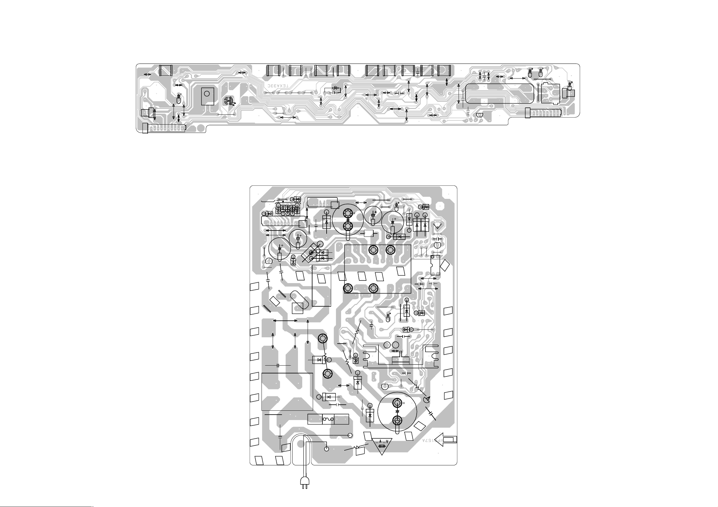
PRINTED CIRCUIT BOARDS
OPERATION
SOLDER SIDE
W015
CD356
SW751_1
W023
CD702
W809
W005
C755A
W808
W016
OS753
D792
R766
W806
Q3801
D3828
D3829
R3808
R3807
SW794
D3827
D3826
C3827
D3825
D3831
W007
W006
C3802
R774
R761A
W004
R3831
CP3803
C3818
C3803
R771
R772
SW791 SW792
R775AR776R777R778
D3822
TP3802
CP3802
C3824_2
R3819
D3817
D3802
D3823
TH3800_1
R773A
SW793
D752
W019
W017
C781
POWER
SOLDER SIDE
TP3801
D3821
D3824
RY3800
C3826
SW795
W018
C3823
B3801
T3800_1
W009
W007
R3802
R3830
SW797
C3822
C702
W011
C3820_1
D3820
SW796
R3801
R3829
W008
W010
D3818
C779A
D3830
C3806
W020
D3801
R3805
IC3800
R3804
W805
W001
W024
W013
D3819
SW799
VR3800
R3800
C3800
R3813
Q3800
C3805
SW798
W002
W014
C704_1
C751A
W812
Q752A
C701
W012
J701_1
W804
W813
C351
R352
R351
CD757_1
C353
J351
C352B
CD355
C3804
R3803_1
CP3800
W004
W809
C3801
L3801
PH3800
W802
W005
D3815
S3802
R3817
F3800
D3816
C3812
R3827
R
W804
FH3800FH3801
3
8
2
R3826
8
S3801
380
R
D3808
C3810
6
2
1
8
3
R
D3810
C3807_1
HS3800
Q3802
D3809
R3832
C3808_1
W003
R3825
C3815
D3807
D3804
D3806
C3811
B3800
Q3803
C3814
R3816
R3821
AS MARKED.
- REPLACE
RISK OF FIRE
R3833
C3816
F-7
F-8
CD3800
Page 43
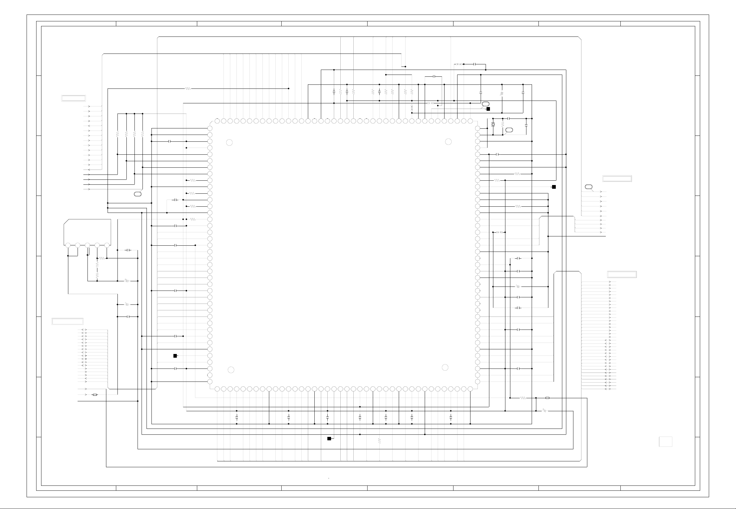
ABC D E F GH
G-1
G-2
MPEG SCHEMATIC DIAGRAM
8
7
6
5
4
3
2
(DVD PCB)
FROM/TO DSP
DVDSTB
DVDSOS
DVDERR
DVDVALID
DVDREQ
DVDDAT0
DVDDAT1
DVDDAT2
DVDDAT3
DVDDAT4
DVDDAT5
DVDDAT6
DVDDAT7
AMCLK
CDERR
CDFRM
CDCLK
CDDATA
1.9V REG.IC
IC4006 PQ070XZ01ZP
VIN
VC
VO
1.9 1.2 0
HD7
HD6
HD5
HD4
HD3
HD2
HD1
HD0
HA4
HA3
HA2
HA1
WR
RD
FCM2012H-102T04
D
GND
6
R4028
B4004
510 +-1%
R4027
12345
5.1 5.1
FROM/TO SYSCON1
MPGCS#
MPGIRQ#
MPGRST
AT+3.3V MD0
P.CON+D5V
VADJ
R4029
1K +-1%
10
GND
R4001 10K
R4002 10K
R4004 10K
R4003 10K
2
C4038
0.1 F
C4043
10016V KA
C4041
10016V KA
C4044
0.1 F
ABCLK
ALRCLK
DVDREQ
DVDSTB
DVDSOS
DVDDAT7
DVDDAT6
DVDDAT5
DVDDAT4
DVDDAT3
DVDDAT2
DVDDAT1
DVDDAT0
R4012
4.7K
MPEG_+1.9V
NC
0 2.0 2.0 1.9 2.2 2.1 1.9 1.9 1.9 2.8 1.61 2.8 3.27 3.27 0 0 1.62 3.24 1.02 1.0 3.24 3.24 0 0 1.63 3.24 0 0 1.18 3.24 0 3.27 0 3.24 1.83
0
110
IDLE
R4023
4.7K
R4024
4.7K
R4025
4.7K
R4026
4.7K
0
3.27
3.27
3.26
0
6
0
0
2.7
9
0
3.24
11
1.84
12
3.24
0
3.24
3.24
2.1
171819 220212223242526272829 330313233343536373839 440
0.9
3.2
0.7
1.5
1.2
1.5
1.4
1.5
3.24
2.7
1.5
1.3
1.7
3.28
3.28
1.89
1.2
0
0.2
3.28
3.24
2.67
NC
0
0.8 0.3 0.3 3.24 0.7 0.3 0.3 0 0.8 0.2 3.24 1.9 0.3 0.8 0 0.3 3.24 3.1 3.2 3.2 1.88 0 0 1.7 3.24 0.9 0 1.5 3.24 0.9 0 0.8 0.9 1.2 3.24 1.5 1.5
C4001
0.1 F
CDERR
CDFRM
CDDATA
CDCLK
C4002
0.1 F
C4003
0.1 F
HD7
HD6 DAC_D
C4004
0.1 F
HD5
HD4
HD3
HD2
HD1
HD0
C4005
0.1 F
HA4
HA3
HA2
HA1 MD0
WR MD15
MPGCS#
C4006
0.1 F
RD MD14
TP4001
MPGIRQ# MD13
C4007
0.1 F
DVDDA6
DVDDA7
DVDDA5
DVDDA4
DVDDA3
DVDDA2
RAD6
RAD1
DVDDA1
RAD7
HWIO
VDDP
1
H0RD
HTYPE
HD15
HD14
HD13
HD12
HD11
GND
HD10
VDOC
HD9
GND
HD8
VDOP
HD7
HD6
VDDIP
HD5
HD4
HD3
HD2
HD1
HD0
VDDP
HA3
HA2
HA1
HA0
HWR
HCS
VDDC
HRD
GND
HROY
HIRQ
VDDP
40 GND
HACK
RAD3
RAD5
VOOP
C4008
RAD2
0.1 F
RAD4
41 42 43 44 45 46 47 48 49550
DVDDA0
DVDREQ
GND
RAD0
51 52 53 54 55 56 57 58 59
DVDVALID
DVDSTRB
DVDVALIO
RAD8
VDDP
C4009
0.1 F
DVDERR
DVDSOS
RAD10
1.2
DVDERR
RAD9
GND
RAD11
R4011 100
R4010 100
C4035 0.1 F
C4034 0.1 F
NC
NC
0
1.89
GND
GPS1
GND
VDDC
GPS0
MPEG IC
IC4001
ZR36732
RAMCS0
VDDP
RAMCS1
60 61 62 63 64 65 66 67 68 69770 71 72 73 74 75 76 77 78 79880
3.1 00.8
C4010
0.1 F
VDDP
ABCK
RAMRAS
RAMCAS
NC NC
0
ALRCK
RAMWE
C4011
0
AOUT2
VDDC
0.1 F
ASDATA0
R4015 33
AOUT1
AOUT0
RAMDQM
GND
CS
R4016 100
C4036 0.1 F
VDDP
PCLK
C4014
SPDIF-DVD
R4017 100
GPIO
VDDP
0.1 F
SPDIF
RDA8
AMCLK
R4018 100
AGND
GND
AMCLK
AMCLK
RDA7
R4019 10K
W837
C4015
VDDAM
VDDP
0.1 F
TEST
RDA9
W829
GND
GND
C4037
0.1 F
VCLKX2
RDA6
VDDP
RDA10
MPGRST
SCNENABL
120
81
RDA12
RDA5
C4016
RESTX
GCLK
VDDP
0.1 F
W818
AGND
PLLCFG0
ICEMODE
CVBS-G-Y
RDA11
C4039
12112212312412512612712812913130131132133134135136137138139141401411421431441451461471481491515015115215315415515615715815916160
STBYX
GCLK1
VDDC
PLLCFG
GND
AIN
VREF
VGND
VGND
RSET
VGND
C-B-U
Y-R-V
VDDD
CVBS-C
VGND
CSYNC
VDDIP
VDDP
HSYNC
VDDP
VSYNC
VCLK
RDA0
RDA15
VDDP
RDA1
RDA14
GND
RDA2
RDA13
VDDP
RDA3
RDA4
0.1 F
VDDA
X0
GND
FI
GND
C4022
1.38
120
1.63
0
1.35
1.88
0
0
0
0.9
0
0
110 111 112 113 114 115 116 117 118 119
1.23
0
1.26
0.6
0.6
3.2
0.6
0.3
0
101 102 103 104 105 106 107 108 109
0.3
100
3.2
3.24
0
1.65
3.0
3.24
0.1
1.65
1.5
0.9
90 91 92 93 94 95 96 97 98 99
3.24
0.9
0.6
0
1.2
1.2
3.24
1.5
1.8
81 82 83 84 85 86 87 88 89
0.1 F
4
NC
NC
NC
NC
NC
C4025_1
TP4007
27MHZ
C4012 3P CH
X4001
100WT02706
C4024
0.1 F
R4006
10K
W806
MPEG_AT+3.3V
R4021
476.3V KA
1M
1
R4007
10K
R4008
390 +-1%
C4027
0.1 F
C4028
0.1 F
C4029_1
476.3V KA
C4030
0.1 F
C4031
0.1 F
C4032
0.1 F
C4033
0.1 F
R4009
C4026
DAC_C
DAC_B
DAC_A
22
GND
GND
GND
0.1 F
C4013
MPEG_AT+3.3V
3P CH
V_REF
FCM2012H-102T04
MD1
MD2
MD3
MD12
B4001
C4017
1506.3V ZL
TP4008
8
7
6
TO AUDIO/VIDEO
3
SPDIF-DVD
AMCLK
ABCLK
ALRCLK
ASDATA0
CS
DAC_A
DAC_B
DAC_C
DAC_D
G_DAC
FROM/TO MEMORY
MA4
MA3
MA5
MA2
MA6
MA1
MA7
MA0
MA8
MA10
MA9
MA11
MCS0#
MRAS#
MPCLK
MCAS#
MWE#
MDQM
MD8
MD7
MD9
MD6
MD10
MD5
MD11
MD4
MD12
MD3
MD13
MD2
MD14
MD1
MD15
5
4
3
2
TP4006
RAM_CS1
MA4
MA3
MA5
MA2
MA6
MA1
MA7
1
NOTE:THIS SCHEMATIC DIAGRAM IS THE LATEST AT THE TIME
OF PRINTING AND SUBJECT TO CHANGE WITHOUT NOTICE
MA0
MA8
MA10
MA9
MA11
MCS0#
MRAS#
MCAS#
MWE#
100
R4005
MPCLK
MDQM
MD8
MD7
NOTE:THE DC VOLTAGE EACH PART WAS
MEASURED WITH THE DIGITAL TESTER
DURING PLAYBACK.
MD9
MD6
MD10
MD5
MD11
MD4
PCB130
VMB261
1
ABC D E F GH
Page 44
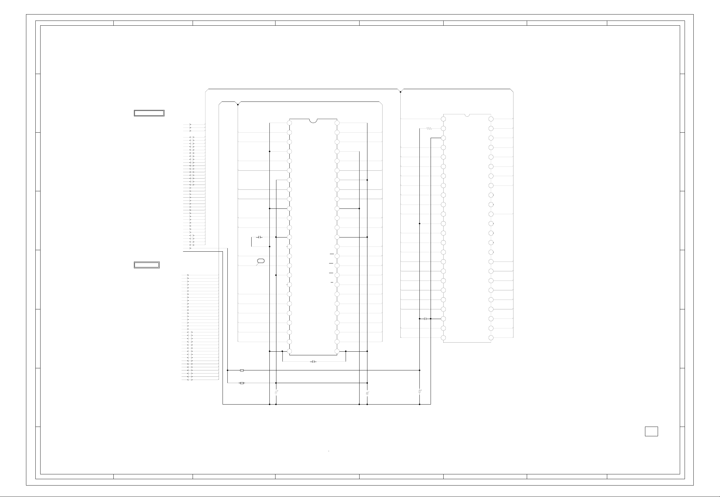
ABC D E F GH
G-3
G-4
MEMORY SCHEMATIC DIAGRAM
8
(DVD PCB)
8
7
S-DRAM IC
VSS
I/O15
I/O14
VSSQ
I/O13
I/O12
VCCQ
I/O11
I/O10
VSSQ
I/O9
I/O8
VCCQ
NC
DQMU
CLK
CKE
NC
A9
A8
A7
A6
A5
A4
IC4002
MSM56V16160F-8
C4019
0.1 F
VCC
I/O0
I/O1
VSSQ
I/O2
I/O3
VCCQ
I/O4
I/O5
VSSQ
I/O6
I/O7
VCCQ
DQML
3.3
WE
CAS
RAS
CS
A11
A10
VCCVSS
C4040
0.1 F
R4030
10016V KA
0.6
3.2
1K
0
1.6
2.0
0.6
0.9
0.6
0.6
40 41 42 43 44 45 46 47 48
0.7
1.5
3.2
1.1
1.1
1.1
1.3
0.6
1.3
1.4
30 31 32 33 34 35 36 37 38 39
1.5
1.1
0
0
25 26 27 28 29
3.2
110111213141516171819 2202122232425
0.5
0.5
3
0
4
1.0
5
0.8
6789
3.2
0.8
0.8
0
0.4
0.7
3.2
0
3.1
3.1
3.0
2.9
0.6
2.2
0.6
A0
0.5
A1
0.5
A2
0.5
A3
3.2
C4020
MDQM
MRAS#
MCS0#
1506.3V ZL
HA17 HA16
HD15 HA13
HD7 HA12
HD14 HA11
HD6 HA10
HD13 HA9
HD5
HD12
HD4 HWRH
HD11
HD3
HD10
HD2 HA19
HD9 HA18
HD1 HA8
HD8 HA7
HD0 HA6
RD HA5
FLASHCS HA3
HA1 HA2
C4045
FROM/TO SYSCON1
0
C4023
50
0
0.9
0
1.2
1.2
3.2
0.9
0.9
0
0.9
40 41 42 43 44 45 46 47 48 49
0.9
3.2
0
NC
0
1.5
3.2
0.1
NC
33 34 35 36 37 38 39
0.3
0.2
0.6
30 31 32
0.6
0.6
0.9
0
26 27 28 29
1506.3V ZL
FLASHCS
RD
HWRH
HD8
HD9
HD10
HD11
HD12
HD13
HD14
6
5
FROM/TO MPEG
4
3
HD15
HA19
HA18
HA17
HA16
HA15
HA14
HA13
HA12
HA11
HA10
AT+3.3V
MA4
MA3
MA5
MA2
MA6
MA1
MA7
MA0
MA8
MA10
MA9
MA11
MCS0#
MRAS#
MPCLK
MCAS#
MWE#
MDQM
MD8
MD7
MD9
MD6
MD10
MD5
MD11
MD4
MD12
MD3
MD13
MD2
MD14
MD1
MD15
MD0
HD7
HD6
HD5
HD4
HD3
HD2
HD1
HD0
HA9
HA8
HA7
HA6
HA5
HA4
HA3
HA2
HA1
GND
D
MD15 MD0
MD14 MD1
MD13 MD2
MD12 MD3
MD11 MD4
MD10 MD5
MD9 MD6
MD8 MD7
C4018
0.1 F
MDQM MWE#
MPCLK MCAS#
MA9 MA11
MA8 MA10
MA7 MA0
MA6 MA1
MA5 MA2
MA4 MA3
B4003
FCM2012H-102T04
B4002
FCM2012H-102T04
5
2
FLASH IC
IC4005
SST39VF800A-70-4C-EK
A16
NC
VSS
DQ15
DQ7
DQ14
DQ6
DQ13
DQ5
DQ12
DQ4
VDD
DQ11
DQ3
DQ10
DQ2
DQ9
DQ1
DQ8
DQ0
DE#
VSS
CE#
A0 A1
A15
A14
A13
A12
A11
A10
WE#
A18
A17
8M
0.5
110111213141516171819 22021222324
0.5
HA15
0.5
HA14
3
0.5
4
0.4
56789
0.5
0.6
A9
2.9
A8
0
NC
NC
0
NC
NC
3.2
0
NC
NC
0
NC
NC
0
NC
NC
0
NC
NC
0
NC
0.3
2.8
2.8
A7
2.8
A6
0.4
A5
2.4
A4
A2
HA4
1.2
1.21.6
7
6
5
4
3
2
PCB130
VMB261
NOTE:THIS SCHEMATIC DIAGRAM IS THE LATEST AT THE TIME
1
OF PRINTING AND SUBJECT TO CHANGE WITHOUT NOTICE
NOTE:THE DC VOLTAGE EACH PART WAS
MEASURED WITH THE DIGITAL TESTER
DURING PLAYBACK.
1
ABC D E F GH
Page 45
8
G-5
G-6
7
6
5
4
3
2
ABC D E F GH
FROM/TO MOTOR DRIVE
FROM/TO MPEG
FROM/TO MEMORY
GND[A]
GND[M]
GND
P.CON+9V
AT+3.3V
SPD_FG
DMUTE
OPEN
CLOSE
LSW
CLS_SW
OPN_SW
P.CON+A5V
HD7
HD6
HD5
HD4
HD3
HD2
HD1
HD0
HA4
HA3
HA2
HA1
MPGCS#
MPGIRQ#
MPGRST
AT+3.3V
GND
P.CON+D5V
FLASHCS
HWRH
HD8
HD9
HD10
HD11
HD12
HD13
HD14
HD15
HD7
HD6
HD5
HD4
HD3
HD2
HD1
HD0
HA19
HA18
HA17
HA16
HA15
HA14
HA13
HA12
HA11
HA10
HA9
HA8
HA7
HA6
HA5
HA4
HA3
HA2
HA1
AT+3.3V
GND
SYSCON1 SCHEMATIC DIAGRAM
(DVD PCB)
EEPROM IC
IC1006
S-24C04BFJ-TB
0
1234
A0 VCC
0
A1
0
A2
0
A3
D
RX
SO2 SO2_82
TX
SI2 SI2
WR
RD
D
RD
R1030
4.7K
R1002
10K
R1001
MPGIRQ# HD14
MPGRST HD13
10K
R1066
10K
TP1005
SYSCON_AT+5V
3.2
0
TEST
3.0
SCL
SDA
D1001
MCL4148
C1016 100P CH
3.0
5678
TP1003
TP1002
SI1
DVDRST
A19/P63
RST#
C1011 0.1 F
C1019 0.1 F
B1001
FCM2012H-102T04
A16/P60
A17/P61
A18/P62
VSS
MD0
MD1
R1023
4.7K
R1053
P57/A15
P56/A14
5251P51/A09
24
25 P20/D16
MD2
P80/RDY
R1054 4.7K
C1021 0.1 F
4.7K
RDY
C1008
565758596606162636465666768697707172737475
P55/A13
P50/A08
P85/WR1#
P81/BGRNT#
R1055 4.7K
SYS_MUTE
0.1 F
R1024
55
P54/A12
P82/BRQ
1.23.33.33.3003.303.33.33.30.13.33.33.33.33.303.33.303.3
R1069 33
RD
4.7K
P53/A11
P83/RD#
3.3
R1070 33
R1067 4.7K
WR
2.82.80.90.80.80.60.60.7 0.70.60.30.10.13.303.03.03.35.15.102.63.32.3 0
P47/A07
P46/A06
P52/A10
P45/A05
P44/A04
P43/A03
P42/A02
P41/A01
P40/A00
P37/D31
P36/D30
P35/D29
P34/D28
P33/D27
P32/D26
P31/D25
P30/D24
P27/D23
P26/D22
P25/D21
P24/D20
P23/D19
P22/D18
P21/D17
P84/WR0#
1.53.3
R1073 33
R1068 4.7K
HWRH
R1074 4.7K
VCC
VSS
AT+3.3V_M
51525354
2.5
50
2.8
0.9
2.5
1.3
1.3
1.7
C1009
3.3
0.1 F
0.1
2.1
0
40 41 42 43 44 45 46 47 48 49
0.9
0.8
1.6
1.2
1.4
1.6
1.4
1.5
0.7
0.7
30 31 32 33 34 35 36 37 38 39
0.7
1.0
1.2
26 27 28 29
JG1004
HD9
47K
R1026
R1027
HD8
R1018
10K
C1005
47K
0.1 F
HD9
B1002
FCM2012H-102T04
W828
DVDRST
C1002
18P CH
R1031
1506.3V ZL
R1015
R1014
10K
C1006
10K
TP1001
C1003
18P CH
10K
R1032
0.1 F
C1012_1
6
4716V KA
10K
R1016 10K
R1003
100K
R1004
4.7K
R1005
4.7K
R1020 10K
R1008
R1010
4.7K
R1009
W808
R1021
PD0/AN0/STRBIN
PD1/AN1/DRVVLD
12DREQ2/PB5/CS1L
DACK2/PB6/CS1H
PB7/DW1#
VCC
3
4
R1037 4.7K
0.1 F
C1014
R1019 4.7K
R1038 10K
4.7K
C1015 0.1 F
AVSS/AVRL
7475PD2/AN2/DVDSOS
PA6/CLK
5
CD/DVD
4.7K
R1051
C1007 2206.3V KA
C1013 0.1 F
R1034 10K
5.1
SI0/PF0
76777879
3.3
SO0/PF1
3.3
SC0/PF2
5.1
SI1/PF3
3.3
SO1/PF4
80818283848586878889
5.2
SI2/PF5
3.2
SO2/PF6
0.3
PF7/INT4/ATG#
NC
3.2
DACK1/PE7
NC
3.3
DACK0/PE6
3.3
DREQ1/PE5
3.3
DREQ0/PE4
2.7
INT3/PE3/SC2
4.7
INT2/PE2/SC1
0
VSS
90919293949596979899
1.7
X1
1.6
X0
3.3
4.7K
R1011
4.7K
4.7K
VCC
3.3
INT1/PE1
3.3
INT0/PE0
3.3
RAS0/PB0
3.2
CSOL/PB1
3.3
CSOH/PB2
3.2
DWOX/PB3
0.1 0.6
PB4/EOP2
100
110
R1036
4.7K
R1039
AVCC
AVRH
PD3/AN3/INIT5
PA5/CS5#
PA4/CS4#
8
R1017 33
R1040 10K
MPGCS#
10K
R1072 33
R1071 33
A23/P67
P70/A24/EOP0
PA2/CS2#
EOP1/PA3/CS3#
9
R1046 4.7K
R1041 4.7K
DVDCS
10K
R1048
R1050 4.7K
VSS
A20/P64
A21/P65
A22/P66
SYSCON IC
IC1001
ZR36705
NMI#
PA1/CS1#
FLASHCS
HST#
PA0/CS0#
11 12 13 14 15 16 17 18 192 20 21 22 23 24 25
R1049 4.7K
R1047 4.7K
R1012
4.7K
C1020
22P CH
C1001
0.1 F
C1017
100P CH
TP1004
SO1
WRQ HD5
X1001
100CT01210
DVDIRQ HD15
TP1006
C1004
JG1002
SCL
SDA
HA19
HA18
HA17
HA16
HA15
HA14
HA13
HA12
HA11
HA10
HA9
HA8
HA7
HA6
HA5
HA4
HA3
HA2
HA1
HA0
HD7
HD6
HD4
HD3
HD2
HD1
HD0
HD12
HD11
HD10
P.CON+D5V
P.CON+A5V
SI2
SO2
VCC+9V
SPDIF
W835
D
GND
GND[A]
P.CON+D5V
P.CON+A5V
AT+3.3V
HD7
HD6
HD5
HD4
HD3
HD2
HD1
HD0
HA12
HA11
HA10
HA9
HA8
HA7
HA6
HA5
HA4
HA3
HA2
HA1
HA0
WR
RD
RDY
DVDRST
WRQ
DVDCS
DVDIRQ
P.CON+A5V
GND[A]
GND
GND[A]
AT+D5V
CPU_RESET
VCC+9V
SYS_MUTE
SCL
SDA
SPDIF
CD/DVD
AT+3.3V
L1001
2.2uH 0305
P.CON+9V
GND[M]
1B
C1018
D
AT+D5V
AT+3.3V
GND[A]
FROM/TO DSP
TO READ CHANNEL
FROM/TO AUDIO/VIDEO
GND
FROM REGULATOR
CD8502
(CP8005)
CU262501
P.CON+5V
GND
P.CON+5V_A
GND
P.CON+9V_A
MOTOR_GND
FROM/TO REGULATOR
CD8501
(CP8001)
CU2D3001
TX
RX
GND
GND
P.CON+9V
P.CON+9V
P.CON+D5V
P.CON+D5V
GND
P.CON+3.3V
P.CON+3.3V
GND
SPDIF-134
L8507
W5T29X7.5X19
PCB130
VMB261
1
8
2
3
4
5
6
1
2
3
4
7
5
6
7
8
9
10
11
12
13
6
5
4
3
2
1
NOTE:THIS SCHEMATIC DIAGRAM IS THE LATEST AT THE TIME
OF PRINTING AND SUBJECT TO CHANGE WITHOUT NOTICE
NOTE:THE DC VOLTAGE EACH PART WAS
MEASURED WITH THE DIGITAL TESTER
DURING PLAYBACK.
1
ABC D E F GH
Page 46
ABC D E F GH
G-7
G-8
DSP SCHEMATIC DIAGRAM
8
7
6
5
FROM/TO READ CHANNEL
4
3
2
(DVD PCB)
FROM/TO MOTOR DRIVE
SPD
SLD
TD
FD
SPD_FG
VREF
P.CON+A5V
VREF
TOST
FOST
BOOT3T
RFVCA
TBAL
FBAL
SGC
ADPH
XHTR
BH
BHDC
RFP
RFN
ADWO
ADTE
TE
ADFE
ADRREC
DEFECTO
DEFECTI
ADBCA
LDON1
CDX4
CDX2
LDON2
DPD_TE
XQBH
DEFINH
W842
C2002
0.1 B
P.CON+A5V
C2006 0.001 B
C2011 0.001 B
C2014 0.001 B
C2009 0.1 B
R2014 15K
R2001 100K
R2002 33K
VREF
TOST CDCLK
FOST CDDATA
BOOT3T CDERR
RFVCA DVDDAT7
TBAL DVDDAT6
FBAL DVDDAT5
SGC DVDDAT4
C2003 0.001 B
DEFINH DVDREQ
CDX2
CDX4
8
CASL
5.001.5
DVSS
X16MIN
DVDD5
TEST2
MDE
MCASU
3031
CASH
WE
MAASO
MWE
MD8_A
MD9_A
MD10_A
1.5
1.5
1.6
MD9
MD8
MD10
DVDCKOUT
DVDCKIN
TEST3
3.303.301.0
OE
RAS
0.1
MD11_A
MD12_A
1.5
1.5
MD11
DVDD0
MA8_A
A8
NC
MD13_A
1.5
MD13
MD12
DVSS
VPDO
101102 103104
100
MD14_A
MD15_A
1.5
MD14
VCOCTL
EFMOUT
AVERRB
AVSCTB
AVDACK
AVACKOI
AVREQIO
VRPFR
1.2
1.003.3
MA7_A
A7
A0
MA0_A
JVRVO
JVAIN
MD15
JVAO
JVCPC
JVCP1
AVSS
AVDD2
AVDD2
CDFR
FISET
PISET
PCN
LF3
LF2
LF1
FPDO
PPDO
DVSS
DVDD0
PCK
LEFM
DVSS
DVDD4
DOUT
EMPH
LRSY
ROMCK
ROMXA
C2F
AVD7
AVD6
AVD5
AVD4
AVD3
AVD2
AVD1
AVD0
DVDD4
DVSS
PP7
PP6
DVDD6
XOUT
XIN
VCOC
DVSS
MA6_A
MA5_A
MA4_A
0
23242526272829
A5
A6
A1
MA1_A
3.301.5
157158159160161162163164165166167168169170171172173174175176177178179180181182183184185186187188189190191192193194195196197198199200201202203204205206207208
105106 107108 109110111 112113 114115 116117118 119120 121122 123124125 126127 128129 130131132 133134 135136 137138139 140141 142143 144145146 147148 149150 151152153 154155 156
MA2_A
0
0
1.4
0
2.6
0
5.0
0.5
0
1.9
1.7
2.9
NC
0.4
NC
0
0.3
2.0
2.0
2.0
0
3.3
1.5
1.6
1.6
0
3.3
0
0
3.3
0
0
3.3
2.0
1.6
1.6
2.0
2.0
2.0
2.0
2.0
3.3
0.1
3.3
3.3
1.7
2.3
0.1
0
3.3
3.3
1.6
1.6
0
A4
A2
A3
5.05.05.05.05.05.05.0
MA3_A
R2035 27K
R2036 10K
R2042 1.2K
R2043 1.8K
R2044 22K
R2045 22K
C2031 0.1 B
R2037 22
SPDIF-CD
CDFRM
DVDSOS
DVDSTB
DVDVALID
R2046
1M
R2041
VSS
VCC
7
1506.3V ZL
C2033
C2041
C2034 0.01 B
C2035 0.1 B
C2036 0.1 B
C2038 0.1 B
TP2018
R2038 10K
R2039 10K
150
C2039
X2001
100CT01604
0.1 B
15P CH
C2040
15P CH
W839
B2003
FCM2012H-102T04
C2045
C2043
150P CH
C2049 0.1 B
R2052 1.2K
R2054 680
TP2015
TP2013
TP2014
1506.3V ZL
C2046
C2048
2206.3V KA
P.CON+A5V
0.1 B
B2001
C2051
B2002
C2053
FCM2012H-102T04
1506.3V ZL
C2050
FCM2012H-102T04
LDON2
LDON1
C2052
1506.3V ZL
1506.3V ZL
0.1 B
MD9_A
MD15_A
MD14_A
MD13_A
4.3 4.3 4.3 04.3 4.3 4.3 4.3 4.3
0
VSS
1506.3V ZL
C2023
DRAM IC
IC2002
C2024
0.1 B
JV
XHTR
DEFECTI
DEFECTO
000
NC NC NC NC NC NC
TP2001
BH
TE
ADWO
ADBCA
ADRREC
ADPH
BHDC
ADTE
ADFE
C2017
RFP
470P CH
C2018
RFN
470P CH
C2019 0.1 B
C2010
2206.3V KA
C2015 0.001 B
C2016 0.001 B
R2017 10K
R2016 10K
C2020 0.001 B
TP2004
TP2002
R2006 1K
R2007 1K
R2008 1K
R2009 1K
R2010 1K
R2011 1K
SLD DVDDAT3
SPD DVDDAT2
TD DVDDAT1
FD DVDDAT0
SPD_FG DVDERR
R2012 10K
R2013 10K
WRQ
TP2005
TP2003
5.0
2.5
110
RFPI
2.5
TESTIO
4.9
3
DVDD2
0
4
DVSS
2.5
5
AD5
2.5
AD4
2.5
AD3
2.5
AD2
0.3
AD1
3.2
AD0
3.2
RF PH
111213141516171819 22021222324
2.3
RF BH
2.5
TE
0.1
FE
0
TEST0
2.5
EFMINP
0
TEST1
2.5
EFMINN
2.5
SLCLPF0
2.5
SLCLPF1
2.5
SLCO1
2.5
SLCO2
5.0
AVDD1
0
AVSS
2.5
VREF
2526272829
2.5
SLCBIAS
2.5
TESBIAS
2.4
HFLBIAS
2.5
OFSET
2.5
BCATH
30313233343536373839
2.4
BOOT3T
3.0
RFVCA
2.5
TBAL
2.4
FBAL
2.6
SGC
2.5
SLDO
2.3
SPDO
2.6
TDO
2.5
FDO
0
DVSS
40414243444546474849
3.3
DVDD0
2.2
FG
3.3
EVENT
2.0
HFLIO
0
PP0
0.1
PP1
0
PP2
3.1
PP3
2.7
WRQ
3.2
HFBUSYB
50
3.3
HBUSYB
5152
3.3
DVDD3
53 545556 57 58 59660 61 62 63 64 65 66 67 68 69770 71 72 73 74 75 76 77 78 79880 81 82 83 84 85 86 87 88 89990 91 92 93 94 95 96 97 98 99
0
NCNC
000
RFP2
RFP3
RFP4
CEFECTO
DVDRESB
RESB
HRDB
HWRB
3.3
3.2
3.3
3.3
1.2
3.3
I/O 15
MSM5416258B-30
VCC
I/O 0
3.3
DVDD0
HDAT1
1.6
0
1.4
MD0_A
MWE
MDE
MCASL
R2022 220
R2021 220
R2020 220
4.6
4.6
4.9
MOEB
MWEB
DVSS
53 DVSS
54 HWAITB
HIRQB55
HDT2
HDAT3
HDAT4
1.2
1.5
0.7
3
MD1_A
MCASLB
HDAT5
5.0 4.2 4.5 5.04.5 4.5 4.54.3 4.3 4.3
5.0
0
RFP0
RFP1
HCSB
HDAT0
3.3
1.4
MD12_A
4041424344
I/O 13
I/O 14
I/O 1
I/O 2
4
56789
MD2_A
MD3_A
MCASU
MAASO
R2024 220
R2023 220
0.2
0.2
5.0
NC
4.2
4.6
MA11
MA12
MRAS0B
MRAS1B
MCASUB
103
AVSS
104
AVDD3
HDAT6
HDAT7
HADR0
HADR1
HADR2
0.9
2.1
0.1
1.7
1.4
I/O 12
I/O 3
1.3
0.2
MA10
HADR3
2.8
VSS
VCC
MA8_A
2.2
0.2
MA9
HADR4
0.8
0
MA8
HADR5
2.8
MD11_A
I/O 11
I/O 4
MD4_A
5.0
DVSS
DVDD5
HADR6
HADR7
1.0
MA7_A
2.6
MA7
HADR8
2.9
MD10_A
MD5_A
MA6_A
2.6
MA6
HADR9
2.9
MD8_A
I/O 8
I/O 9
I/O 10
I/O 5
I/O 6
I/O 7
10 13 141 15 16 17 18 192 20 21 22
MD6_A
MD7_A
MA5_A
MA4_A
MA3_A
MA2_A
MA1_A
MA0_A
MD0_A
MD1_A
MD2_A
MD3_A
1.5
1.5
1.5
1.4
2.6
2.6
2.6
2.6
2.6
2.6
MD2
MD1
MD0
MA0
MA1
MA2
MA3
MA4
MA5
DSP IC
IC2001
LC78661W
HADR10
HADR11
0.9
0.7
HADR12
0.7
3.303.3
53
54
55
DVDD3
DVSS
DEFECT1
DVSS
DVDD1
PW/FSEQ
SBCK
3.3
SBSY
0.1
157
158
SFSY
000
MCASL
NC
5.0 5.0 5.0 5.0 5.0 5.0 5.0 5.0
0
323536373839
00
NC
NC NC
MD4_A
MD5_A
MD6_A
MD7_A
1.5
1.5
1.4
MD7
MD6
MD5
MD4
MD3
AVDD4
AVSS
FSX
EFLG
PP4
PP5
X16MOUT
3.3
3.201.701.2
FROM/TO SYSCON1
D
GND
GND[A]
P.CON+D5V
P.CON+A5V
AT+3.3V
HD7
HD6
HD5
HD4
HD3
HD2
HD1
HD0
HA12
HA11
HA10
HA9
HA8
HA7
HA6
HA5
HA4
HA3
HA2
HA1
HA0
WR
RD
RDY
DVDRST
WRQ
DVDCS
DVDIRQ
TO AUDIO/VIDEO
SPDIF-CD
FROM/TO MPEG
DVDSTB
DVDSOS
DVDERR
DVDVALID
DVDREQ
DVDDAT0
DVDDAT1
DVDDAT2
DVDDAT3
DVDDAT4
DVDDAT5
DVDDAT6
DVDDAT7
CDERR
CDFRM
CDCLK
CDDATA
AMCLK
7
6
5
4
3
2
NOTE:THE DC VOLTAGE EACH PART WAS
MEASURED WITH THE DIGITAL TESTER
DURING PLAYBACK.
1
NOTE:THIS SCHEMATIC DIAGRAM IS THE LATEST AT THE TIME
OF PRINTING AND SUBJECT TO CHANGE WITHOUT NOTICE
ABC D E F GH
DVDRST
R2064
220
RDY
DVDIRQ
C2021
TP2010
TP2009
TP2008
0.1 B
DVDCS
RD
WR
HD0
HD1
HD2
HD3
HD4
HD5
HD6
HD7
HA0
HA1
HA2
HA3
HA4
HA5
HA6
HA7
TP2022 TP2012 TP2023
HA10
HA11
HA12
HA8
HA9
TP2007
R2025 10K
TP2006
XQBH
TP2011
R2028 22
R2026 10K
R2027 10K
R2029 10K
DPD_TE
R2030 5.6K
C2030
0.1 B
R2031
10K
R2033
220
C2032
0.1 B
C2037
0.1 B
8
16MHZ
W810
PCB130
VMB261
1
Page 47
ABC D E F GH
G-9
G-10
MOTOR DRIVE SCHEMATIC DIAGRAM
8
(DVD PCB)
8
TO READ CNANNEL
FO+
FO-
SLD1
SLD2
SP1+
SP1-
+5V
SP_FG
GND
LIMIT_SW
TR+
TR-
C2309
10016V KA
C2310
0.1 B
TR-
TR+
FO-
FO+
C2301
0.1 B
C2303
0.1 B
C2306
0.1 B
R2308
7
6
5
CD2301
2H081007
FROM/TO LOADER
CP2301
00_6232_008_102
1
2
3
4
5
6
7
8
4
P.CON+9V
CLOSE
OPEN
R2314
12K
MOTOR DRIVE IC
IC2301 LA6560
0
1101112131415161718
FWD
0
2
REV
9.1
3
VCC2
0.2
456789
VLD-
0.2
VLD+
4.0
VD4+
4.3
VD4-
4.3
VD3+
4.1
VD3-
0
37
5.3
VD2+
3.1
VD2-
4.2
VD1+
4.2
VD1-
9.1
VCC1
2.5
15K
VIN1
0
VIN1-A
2.5
VIN1+A
VIN1-B
S-GND
VCONT
MUTE
VIN4
VIN4-
VIN4+
VREF-IN
VIN1-SW
VREF-OUT
REG-OUT
REG-IN
VIN3+
VIN3-
VIN3
VIN2+
VIN2-
VIN2
VIN1+B
0
4.2
3.3
R2313
2.5
10K
2.5
2.5
2.6
30 31 32 33 34 35 36
5.0
2.5
NC
0
38
0
NC
0.9
26 27 28 29
NC
2.5
2.5
2.6
2.5
2.5
3.0
20 21 22 23 24 25
2.52.5
19
R2315
22K
R2316
10K
R2318
R2317
5.6K
R2319
10K
10K
R2320
10K
DMUTE
FD
SPD
TD
FROM/TO SYSCON1
P.CON+9V
AT+3.3V
SPD_FG
DMUTE
OPEN
CLOSE
LSW
CLS_SW
OPN_SW
GND
GND[M]
GND[A]
P.CON+A5V
7
6
5
4
FROM/TO LOADER
CP2302
A2001WR2-5P
MLD1(-)
CD2302
CU251002
1
MLD2(+)
2
CLOSE
3
GND(D)
4
OPEN
5
3
R2306
R2302
10K
R2321
2
R2301
10K
22K
0.4
15K
C2305
0.1 B
C2304
0.1 B
10K
R2304
1.6
0
SPDFG.CTL
Q2301
KTC3875S_Y_RTK
R2303
10K
KTA1504S_Y_RTK
R2305
10K
SPDFG.CTL
Q2304
10K
R2322
3.0
C2308
0.1 B
3.3
R2310
10K
2.3
DMVTE_CTL
R2323 1M
C2307 0.0022 B
R2309
100
Q2302
KTA1504S_Y_RTK
DMVTE_CTL
KRC102SRTK
R2311
100
Q2303
4.9
R2312
100
R2324
5.0
R2307
4.2
10K
1K
0
3.3
0
P.CON+A5V
VREF
SLD
SPD_FG
DMUTE
LSW
CLS_SW
OPN_SW
C2315
0.1 B
FROM/TO DSP
SPD
SLD
TD
FD
SPD_FG
VREF
P.CON+A5V
PCB130
VMB261
3
2
CAUTION: DIGITAL TRANSISTOR
1
NOTE:THIS SCHEMATIC DIAGRAM IS THE LATEST AT THE TIME
OF PRINTING AND SUBJECT TO CHANGE WITHOUT NOTICE
NOTE:THE DC VOLTAGE EACH PART WAS
MEASURED WITH THE DIGITAL TESTER
DURING PLAYBACK.
1
ABC D E F GH
Page 48
8
G-11
G-12
7
6
5
4
3
2
1
DVD LOADER
DK4001
DVD-KDR717SK
FROM/TO LOADER
CD2601
2H0O2102
0.5mm PITCH FFC
CP2601
24FLZ-RSM1-TB
F-
24
F+
23
T+
22
T-
21
20
19
B
18
A
17
E
16
GND-PD
15
VC
14
VCC
13
F
12
D
11
C
10
CD/DVD
9
8
VR-CD
7
VR-DVD
6
MD
5
LD-CD
4
HFM
3
2
LD-DVD
1
GND-LD
ABC D E F GH
READ CHANNEL SCHEMATIC DIAGRAM
TP2602
GND[A]
C2619
150P CH
Q2606
NC
NC
NC
FROM MOTOR DRIVE
FO+
FO-
TR+
TR-
0.7
5.0
2.6
KTC3875S_Y_RTK
2.2K
R2670
R2671
0
KTC3875S_Y_RTK
DPD_TE_CTL
R2608
CDX2_CTL
KTC3875S_Y_RTK
0
CDX4_CTL
Q2601
KTC3875S_Y_RTK
0
C2605
82P CH
PD_CTL
Q2614
10K
0
0.7
DPD_TE_CTL
Q2615
Q2616
KTC3875S
Y_RTK
3.9
4.6
22
R2609
22
R2610
22
R2611
22
0
0.1
5.0
CDX2
CDX4
2.2K
2.2K
FCM2012H-102T04
4716V KA
C2659
C2608
D2601
D2602
KDS120RTK
C2602_1
0.1 B
R2631
FO-
FO+
TR+
TR- XQBH
R2642
PD1
PD2
PD3
PD4 DEFECTO
LDS1_2
C2653
0.1 B
B2601
B2606
-102T04
FCM2012H
C2601_1
C2658
0.1 B
R2604
0.1 B
3.2
2.6
PD_CTL
Q2605
KTA1504S_Y_RTK
R2643 2.2K
R2650 2.2K
R2607 82K
123
KDS121RTK
0
0
123
4716V KA
1K
R2667
0
R2606
82K
CD_CTL
Q2612
2SK3018
S
0
D
S
0
D
0
R2605
1K
2.2K
3.2
R2669
G
100K
DVD_CTL
Q2613
2SK3018
G
3.1
0.7
R2673
10K
R2674
10K
0
R2675
0.7
R2672
100K
C2609
0.001 B
2.6
DVD_LD_CTL
2SA1036K
C2611
1016V KA
0
0
C2613
10K
Q2603
C2610
0.001 B
5.0
CD_LD_CTL
Q2604
2SA1036K
C2612
1016V KA
1K
R2621
C2615
39P CH
R2620
560
PVR
47P CH
2.6
2.6
2.6
PD1
2.6
PD2 XHTR
2.6
PD3
2.6
PD4
0.4
NC
0.4
NC
0.4
NC
2.6
PD8
2.6
PD9
DPD_TE
C2614
R2614
0.1 B
10K
5.1
R2617
3.1
1K
0.2
LDS1_2
R2618
5.1
1K
0.2
1.9
SGC
2.5
FBAL
2.5
TBAL RFP
DEFECTO
0 0 0.1 2.5 2.5 2.5 2.5
VSS
10 11 12 13 14
89
R2623
470
C2616
56P CH
2.7 2.6 2.8 2.5 5.0 2.6 0 2.5 3.2 2.6 0 2.5 0 2.6 5.0 2.6 2.6 3.2 2.6 3.0
110111213141516171819 220
RFN
RFP
PD1
PD2
5
PD3
6
PD4
PD5
PD6
9
PD7
PD8
PD9
VCC
LDD1
LDS1
LDD2
LDS2
0
GND
SGC
FEBL
TEBL
21 22 23 24 25 26 27 28 29330 31 32 33 34 35 36 37 38 39440
R2622
RFVCA
C2617
27K
PREF
BST
BOOT3T
C2656
150P CH
CA0
80 CAN
VGA21
FOST
2.6
FOST
C2618
2206.3V KA
0.1 B
ADFE
234567
R2625
10K
EQ01
TOST
TOST
R2626
VDD
5.05.05.000.15.00
C2620
1
R2603
RFSCT
BCATH
NC 2.61.22.62.62.52.80.91.22.62.62.62.62.92.62.602.72.72.9
27K
C2649
0.1 B
330
R2627
10K
C2623
EQL1
REFI
150V KA
C2622
C2621
150P CH
IC2601
BU4066BCF
DEFE CTL IC
33P CH
GND
SREF
150P CH
R2628 330
EQ02
RREC
R2629
ADRREC
R2630
LDON1
2.2
R2619
LDON1
READ CHANNEL IC
FE
27K
330
EQI2
IC2602
LA9702WL
TE
ABC D E F GH
LDON2
LDON2
THC
C2625
TP2021
R2632
6.8K
0.1 B
(DVD PCB)
C2626
68P CH
C2627
220P CH
R2634
330
EQI1
EQ01
PP/TE
WO
WOI
ISET
NC NC
56K
R2633
TE
ADTE
C2629
560P CH
NOTE:THIS SCHEMATIC DIAGRAM IS THE LATEST AT THE TIME
NOTE:THE DC VOLTAGE EACH PART WAS
R2640
R2638 150
330
VCC
RF02
RF01
40 RFON
WOO
TEO
TEN
R2639
68K
C2631
33P CH
R2615
12K
TBAL
ADWO
OF PRINTING AND SUBJECT TO CHANGE WITHOUT NOTICE
MEASURED WITH THE DIGITAL TESTER
DURING PLAYBACK.
DPD_TE
C2633
W814
DPD/TE
CP
47P CH
R2644
R2645
EQI3
BHI
330
EQO3
XQBH
EQI4
XHTR
EQO4
EQL2
EQO2
DEFC
RFOP
22K
616263646566676869770717273747576777879880
VCC
CPOF
LPC
GND
BCA
CDX2
TH
TC
DEF
PH
PHI
BH
TP2019
RFN
9
C2634
100P CH
2.6
60
3.2
2.6
5.1
2.6
5.0
2.6
0
2.6
0
2.6
50 51 52 53 54 55 56 57 58 59
0
1.2
3.7
0
5.0
NC
3.0
1.2
2.5
2.6
41 42 43 44 45 46 47 48 49
R2646
C2637
56P CH
C2635_1
C2636
82P CH
TP2020
47K
4716V KA
10
R2649
47K
R2647
2.2K
R2651
330
R2652
330
R2653
R2655
33K
47K
R2656
47K
BH_SW
Q2607
2SK3018
R2654
C2639
0
0
S
C2640
0.0047 B
47K
220P CH
C2641
33P CH
R2657
330
R2662
2.2K
TE_CTL
Q2608
KTC3875S_Y_RTK
0.7
R2659
100K
C2642
22P CH
R2666
G
22K
5.1
D
2.52.5
33K
R2658
R2660
22K
P.CON+A5V
RF5
C2644
18P CH
R2663
10K
R2665
22K
22K
220P CH
BH_SW
Q2610
C2646
W815
5.0
5.0
0
R2668
C2647
47P CH
C2643
470P CH
R2664
5.0
DEFECT CTL
0
Q2609
0
KTC3875S_Y_RTK
R2661
27K
C2645
150P CH
0
0.6
KTC3875S_Y_RTK
0
CRITICAL FOR SAFETY,USE ONES
DESCRIBED IN PARTS LIST ONLY
DANGEREUSES AN POINT DE VUE SECURITE
N’UTILISER QUE CELLS DECRITES
DANS LA NOMENCLATURE DES PIECES
DEFECT CTL
Q2611
KTA1504S_Y_RTK
22K
8
7
6
5
4
3
DPD_TE
DEFECTI
DEFINH
ADBCA
ADPH
XHTR
BHDC
SE5
DP5
B2602
FCM2012H-102T04
476.3V KA
C2652
C2648
0.1 B
B2604
FCM2012H-102T04
C2650
C2651
BH
476.3V KA
0.1 B
C2654
B2605
FCM2012H-102T04
476.3V KA
C2655
0.1 B
FROM SYSCON1
P.CON+A5V
GND[A]
FROM/TO DSP
VREF
TOST
FOST
BOOT3T
RFVCA
TBAL
FBAL
SGC
ADPH
XHTR
BH
BHDC
RFP
RFN
ADWO
ADTE
TE
ADFE
ADRREC
DEFECTO
DEFECTI
ADBCA
LDON1
CDX4
CDX2
LDON2
DPD_TE
XQBH
DEFINH
2
PCB130
VMB261
ARESINCE THESE PARTS MARKED BYCAUTION:
1
ETANTLES PIECES REPAREES PAR UNATTENTION:
Page 49
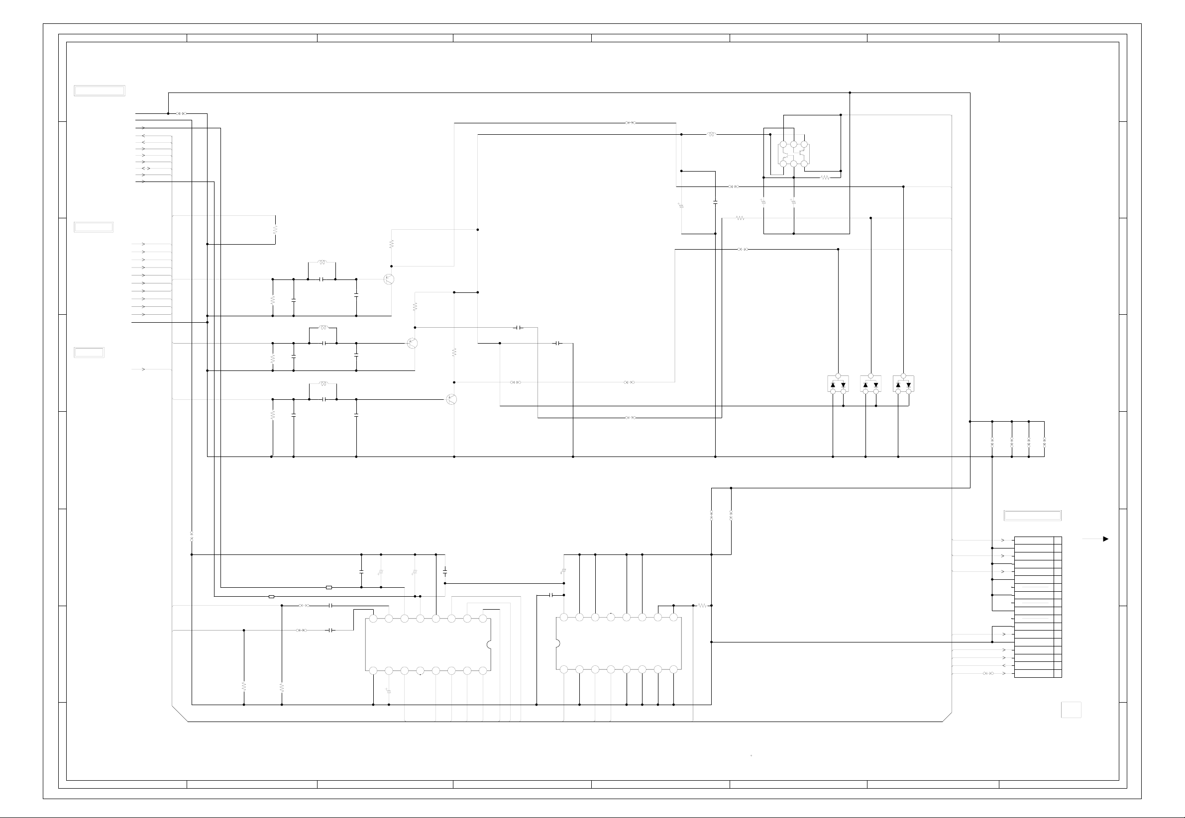
8
G-13
G-14
7
6
5
FROM/TO SYSCON1
FROM MPEG
FROM DSP
ABC D E F GH
AUDIO/VIDEO SCHEMATIC DIAGRAM
GND[A]
AT+D5V
SPDIF
CPU_RESET
VCC+9V
SYS_MUTE
CD/DVD
AT+3.3V
SPDIF-DVD
AMCLK
ABCLK
ALRCLK
ASDATA0
DAC_A
DAC_B
DAC_C
DAC_D
G_DAC
SPDIF-CD
(DVD PCB)
W833
D
GND
SCL
SDA
DAC_A
R8501
75 +-1%
2.2K
0.6
330P CH
KTA1504S_Y_RTK
330P CH
330P CH
R8506
1.2
BUFFER
Q8502
KTA1504S_Y_RTK
0
0.6
BUFFER
Q8503
R8507
0
2.2K
1.2
2.2K
R8508
1.2
BUFFER
Q8504
0.6
KTA1504S_Y_RTK
0
C8518
1B
C8520
0.1 F
L8502
1.8uH
C8502
C8504
C8505
C8508
22P CH
270P CH
L8503
1.8uH
C8509
22P CH
270P CH
L8504
1.8uH
C8510
22P CH
270P CH
C8512
C8513
C8514
CS
DAC_D
DAC_C
DAC_B
R8502
R8503
R8504
75 +-1%
75 +-1%
75 +-1%
W802
W803W841
W804
C8523
10016V KA
L8505
15uH 0305
C8524
0.1 F
W830
R8515
75 +-1%
W840
C8525
9.4
456
12010V ZL
9.2 8.5
9.28.5 9.4
C8526
123
12010V ZL
REG.
Q8506
HN1C03F_B
R8516 680
123
D8504
1SS226
123
D8505
1SS226
123
D8506
1SS226
VCC+9V
DAC/D[CVBS]
CVBS
DAC/C[C]
C(CVBS)
DAC/B[Y1]
Y(G)
8
7
6
5
W827
W831
W832
W834
4
GND[A]
W801
W838
W836
3
AUDIO_L
AUDIO_R
B8502
FCM2012H-102T04
W821
W822
B8501
FCM2012H-102T04
C8529
2.2 F
C8530
2.2 F
226.3V KA
C8536
C8506
0.1 F
2.6 2.6 5.2 3.2 0 3.1 3.1 3.1
VOUTL
VOUTRAGND
VCC
C8537
226.3V KA
VDD
C8538
DGND
0.1 F
LRCK
2345678
DATA
1
BCK
2
R8522
100K
R8523
STEREO DAC IC
100K
IC8503 PCM1748E
9
VCOM
10 11
C8503
ZEROR/ZEROA
ZEROL/NAMDMC
12 13 14 15 16
NC
1016V KA
ZERO
SDA
ML
SCK
3.12.93.03.03.02.92.60
ALRCLK
ASDATA0
AMCLK
ABCLK
CS
SCL
10016V KA
C8534
C8535
0.1 F
000 00003.2
VCC
IC8504
SN74LV4052APW
Y0
DIGITAL AUDIO SW IC
2345678
1
1.6 0
SPDIF-DVD
NC
13141516
X
X1
X2
Y2
Y3
Y
1.6 00000
SPDIF-CD
SPDIF
101112
X3
Inhibit
A
VEE
X0
Y1
R8520
1K
9
B
GND
CD/DVD
DAC/B[Y1]
DAC/C[C]
DAC/D[CVBS]
AUDIO_L
AUDIO_R
ZERO
CPU_RESET
SYS_MUTE
W811
FROM/TO REGULATOR
CP8502
IMSA-9604S-18Z14
Y(G)
GND
C(CVBS)
GND
CVBS
GND
NC
GND
NC
GND
NC
GND
AUDIO-L
GND
AUDIO-R
ZERO
DVD_RESET
SYS_MUTE
(CP8002)
18
17
16
15
14
13
12
11
10
9
8
7
6
5
4
3
2
1
PCB130
VMB261
FFC(1.25P)
CD8002
2H0I0102
4
3
2
1
NOTE:THE DC VOLTAGE EACH PART WAS
MEASURED WITH THE DIGITAL TESTER
DURING PLAYBACK.
NOTE:THIS SCHEMATIC DIAGRAM IS THE LATEST AT THE TIME
OF PRINTING AND SUBJECT TO CHANGE WITHOUT NOTICE
1
ABC D E F GH
Page 50

ABC D E F GH
G-15
G-16
FROM/TO POWER
CP8004
(CP3803)
8
B2013H02-10P
1
2
3
UNREG+12V
4
UNREG+8V
5
UNREG+5V
6
POWER_FAIL
7
STANDBY_H
8
DEGAUSS_H
9
SOUND+B
10
SOUND_GND
GND
GND
5V REG
IC3000 KIA78R05PI
7
TO SYSCON1
CP8005
(CD8502)
A2001WV2-6P
1
P.CON+5V
2
3
P.CON+5V A
4
5
P.CON+9V A
6
MOTOR_GND
GND
GND
11.0
6
(CD8501)
TX
RX
GND
GND
P.CON+9V
P.CON+9V
P.CON+D5V
P.CON+D5V
GND
P.CON+3.3V
P.CON+3.3V
GND
SPDIF-134
(CP8502)
Y(G)
GND
C(CVBS)
GND
CVBS
GND
GND
AUDIO-L
AUDIO-R
ZERO
DVD RESET
SYS MUTE
GND
GND
GND
S106X
S803Y
W894
W872
HS3000
763WSA0018
W862
NC
NC
NC
S805Y
C3003
C3005
0.1 F
0.1 F
C3007
TO ANGLE,DECK
CD8002
2H0I0102
FROM/TO SYSCON1
CP8001
A2001WV2-13P
1
2
3
4
5
6
7
8
9
10
11
12
13
FROM/TO AUDIO/VIDEO
CP8002
IMSA-9604S-18Z14
1
2
3
4
5
6
7
8
9
10
11
12
13
14
15
16
17
18
5
4
3
2
OUT INGNDSW
0 5.0 8.0
C3015
4706.3V YK
C3011
9V REG
IC3001 KIA78R09API
OUT INGNDSW
0 9.0 12.911.0
C3012
W819
D3000
1SS133
C3009
0.1 F
470P CH
C3010
W905
W830
C3014
470P CH
C3026
4.7P CH
R3011_1
8.2K 1/2W
D3007
MTZJ6.8B
1234
C3016
47010V YK
4706.3V YK
47016V YK
R3000
100
1234
POWER_FAIL
STANDBY_H
DEGAUSS_H
HS3001
763WSA0018
47016V MHE
R3001
100
SPDIF-134
W861
DVD_Y
DVD_C
DVD_VIDEO
DVD_A_OUT_L
DVD_A_OUT_R
ZERO
DVD_RESET
SYS_MUTE
S104X S105X
UNREG+12V
TX
RX
W855
S106Y
S803X
D3002
11E1-EIC
CC002
TP-1S-05
W864
C3019
D3006
11E1-EIC
DRIVER
Q3000
2SB1131
13.1 12.6
R3002
12.8
10K
R3003
1K 1/4W
12.8
0
IC3002 KIA78R05PI
1234
8.0 5.0 0 11.0
C3018
1016V KA
R3004
R3005
100 1/2W
SW
Q3001
KRC102SRTK
5.1
5V REG.
OUTIN GND
47016V YK
10006.3V YK
C3020
3.3V OUT
Q3003
2SB1143
3.2
3.1
1.8
1.0
3.3V CTL
Q3002
KTC3875S_Y_RTK
R3006
560
330
D3003
MTZJ12B
SW
R3007
100
3.43.9
REGULATOR SCHEMATIC DIAGRAM
(AV PCB)
82
2235V YK
R3013
C3022
3.9
1.8
1.0
3.3V CTL
Q3004
KTC3875S_Y_RTK
100
R3008
DRIVER
Q3005
KTC3209_Y
11.9 9.0
9.6
R3009
390
D3004
D3005
MTZJ9.1B
1SS133
R3014
R3015
820 +-1%
1.5K
+-1%
P.CON+9V
C3024
100P CH
C3025
4706.3V YK
R3012
100 1/4W
5V REG.
IC3003 KIA78R05PI
1234
8.0 5.0 0 12.6
4706.3V YK
C3028
P.CON+12V
SWIN OUT GND
P.CON+5V
5V REG. IC
IC3004 KIA78R05PI
IN
OUT GND SW
123
8.0
5.0 0 1.9
FBT+12V
4
NC
C3013
TO SOUND AMP
SOUND_GND
SOUND+B
P.CON+9V
P.CON+5V
GND
TO COMB FILTER
P.CON+5V
GND
TO STEREO
P.CON+5V
GND
TO AV SW
GND
P.CON+9V
DVD_VIDEO
TO VIF/SIF/CHROMA
1006.3V YK
DVD_Y
DVD_C
P.CON+5V
P.CON+9V
GND
FROM/TO DEFLECTION
FBT+12V
P.CON+5V
UNREG+12V
GND
8
7
6
5
4
FROM/TO MICON/TUNER
GND
POWER_ON_H
STANDBY_H
DVD_RESET
POWER_FAIL
RX
TX
DEGAUSS_H
P.CON+5V
AT+5.6V
TO IN/OUT
AT+5.6V
P.CON+9V
P.CON+D5V
P.CON+12V
SPDIF-134
SYS_MUTE
DVD_A_OUT_L
DVD_A_OUT_R
ZERO
GND
PCB250
TMB543
3
2
1
DANGEREUSES AN POINT DE VUE SECURITE
N’UTILISER QUE CELLS DECRITES
DANS LA NOMENCLATURE DES PIECES
ETANTLES PIECES REPAREES PAR UNATTENTION:
CRITICAL FOR SAFETY,USE ONES
DESCRIBED IN PARTS LIST ONLY
ARESINCE THESE PARTS MARKED BYCAUTION:
NOTE:THE DC VOLTAGE EACH PART WAS
MEASURED WITH THE DIGITAL TESTER
DURING PLAYBACK.
NOTE:THIS SCHEMATIC DIAGRAM IS THE LATEST AT THE TIME
OF PRINTING AND SUBJECT TO CHANGE WITHOUT NOTICE
CAUTION: DIGITAL TRANSISTOR
DIGITAL AUDIO SIGNAL(PB)
PLAYBACK LUMINANCE SIGNAL
PLAYBACK COLOR SIGNAL
PLAYBACK VIDEO SIGNAL
AUDIO SIGNAL(PB)
1
ABC D E F GH
Page 51

ABC D E F GH
G-17
G-18
MICON/TUNER SCHEMATIC DIAGRAM
R144
4.7K
R145
4.7K
Q103
C119
R001
R148
1006.3V KA
IC199
MEMORY IC
TU001 TECC1040PG32E
IF
BTL
9
11
10
14 15
NC
28.8
C001
75
0.022 MMTS
+30V
TUNER_IF
1K
R149
V-BUFFER
Q105
KTC3875S_Y_RTK
5.0
0
0
C127
W840
S-24C08ADPA-01
1K
C002
0.0082 B
8
NC
4.9
L001
4706.3V YK
R160
BPL
7
100uH 0305
C006
P.CON+5V
R157
R159
33K
2.2K
R162
V.S
6
NC
R003
476.3V KA
SDA
1K
R161
10K 1/4W
15K
SDA
5
4.404.2
100
R004
SCL
R190
SCL
ADRES
3
4
NC
R005
15K
100
C003
0.3
0
4.7K 1/4W
AGC
2
1
12 13
NC
1.6
C005
C004
100P CH
120K
R006
100P CH
R178
0.6
4.7K
BUFFER
Q109
KTC3875S_Y_RTK
3.350V KA
TUNER_AGC
C123_1
SCL
SDA
I2C_OFF
R174
TUNER_AGC
100 1/4W
0.0012 B
POWER_FAIL
C109
W805
TEST
OVDD(OVSS)
UART_CLK_IN
H_CONTROL
10K
R122
H_CONTROL
(AV PCB)
1K
W806
R134
R135
C128
0.01 B
0.022 B
25
26
V-SYNC
OVCC(OVDD)
AFT
X-RAY IN
(FM POWER)
68K
R177
AFT
C106
0.1 B
820
H-SYNC
KEY1
R114
C111
OSD Y/BLK
KEY2
R120
4.7K
270P CH
W844
W847
OSG B
TV/DVD
4.7K
TV/DVD
2223242526272829
OSD G
OSD RIIC BUS OFF
DEGAUSS-H
(FM CE/DEGAUSS)
5.204.15.25.22.3005.25.23.73.75.205.13.205.2000
4.7K
R130
R109 4.7K
DEGAUSS_H
I2C_OFF
R143
4.0 0
0000
R140
100
R141
4.7K
H-BUFFER
4.2
SCL
E2
100
0
C117
MODE
E1
KTC3875S_Y_RTK
0
0.01 B
VCC
E0
1234
4.7K
R142
SCL
SDA
100
R147
4.0 5.2
5678
SDAVSS
8
R119
10K
5.0
SW
Q104
KTA1504S_Y_RTK
7
SDA
NCNC
0.30.2
REMOCON
IC103
RESET IC
PST3245NR
5.2
NC
OUT
123
6
5
4
45
NC
GND
IN
5.2
0
10K
R101
C101
D101
1SS133
10K
R103
336.3V KA
C102
0.01 B
C104
0.1 B
C103
2206.3V KA
D105
SWD_V_OUT
C107
C108
0.1 B
0.1 B
404142
VDD
IC101 OEC6070BMICON IC
VSS
1 101112131415161718192 20 21
1SS133
(FM DATA)
VIDEO IN 1
VIDEO IN 2
PROTECT
X-RAY TEST
3
X_RAY_TEST
PROTECT
(FM CLK)
4
A_MUTE
SCL
W812
W814
REMOCON
4.7K
R110
VVSS
TV MUTE
R115
4.7K
22 23
24
SD
SCL
SDA
DVD RESET
DVD_RESET
POWER_ON_H
POWER
EXT MUTE
56789
EXT_MUTE
4.2
5.0
D104
10K
R123
W838
(REMOCON)REMORT
STANDBY_H
STANDBY_H
R125
MTZJ6.8B
3.3K
123
X101
CSTLS16M0X53-A0
W863
C124
0.1 F
5.24.75.10.24.33.902.92.65.2 2.42.1 005.25.04.2 0000
RESET
POWER FAIL
UART_CLK_OUT
UART_START_BIT
4.7K
10K
R132
R126
RX
X OUT
RX
30313233343536373839
X IN
TX
10K
R129
TX
3
FROM/TO OPERATION
(CD757_1)
CP102
A2001WR2-9P
REMOCON_OUT
1
2
GND
3
AT+5.6V
POWER_ON_LED
4
5
KEY_A
6
7
2
8
KEY_B
9
C132
0.1 F
C133
0.1 F
NC
NC
NC
C134
0.1 F
C135
0.1 F
B.SIGNAL
G.SIGNAL
R.SIGNAL
LUMINANCE SIGNAL
TUNER VIDEO SIGNAL
PLAYBACK VIDEO SIGNAL
1
TUNER AUDIO SIGNAL
AUDIO SIGNAL
AUDIO SIGNAL(PB)
DEFLECTION SIGNAL
DANGEREUSES AN POINT DE VUE SECURITE
N’UTILISER QUE CELLS DECRITES
DANS LA NOMENCLATURE DES PIECES
ETANTLES PIECES REPAREES PAR UNATTENTION:
CRITICAL FOR SAFETY,USE ONES
DESCRIBED IN PARTS LIST ONLY
ARESINCE THESE PARTS MARKED BYCAUTION:
NOTE:THE DC VOLTAGE EACH PART WAS
MEASURED WITH THE DIGITAL TESTER
DURING PLAYBACK.
NOTE:THIS SCHEMATIC DIAGRAM IS THE LATEST AT THE TIME
OF PRINTING AND SUBJECT TO CHANGE WITHOUT NOTICE
ABC D E F GH
TEST POINT
07JQ-ST
GND
I2C SCL
I2C SDA
I2C OFF
AGC
AUDIO OUT L
AUDIO OUT R
FROM/TO IN/OUT
EXT_MUTE
TV/DVD
AUDIO_OUT_R
AUDIO_OUT_L
FROM/TO VIF/SIF/CHROMA
OSD_Y
OSD_B
OSD_G
OSD_R
SDA
SCL
TV/DVD
SYNC_VIDEO
H_CONTROL
PROTECT
AFT
TUNER_AGC
TUNER_IF
FROM/TO DEFLECTION
VD
AFC
X-RAY
X_RAY_TEST
+30V
FROM/TO REGULATOR
GND
POWER_ON_H
STANDBY_H
DVD_RESET
POWER_FAIL
RX
TX
DEGAUSS_H
P.CON+5V
AT+5.6V
FROM/TO AV SW
SWD_V_OUT
SDA
SCL
FROM/TO SOUND AMP
POWER_ON_H
A_MUTE
SCL
SDA
FROM/TO STEREO
SCL
SDA
CP101
8
1
2
3
4
5
6
7
7
6
5
4
3
2
PCB250
TMB543
1
Page 52

ABC D E F GH
G-19
G-20
VIF/SIF/CHROMA SCHEMATIC DIAGRAM
8
(AV PCB)
SW
Q601
KTC3875S_Y_RTK
9.0
0
0.3
R626
1K
H_CONTROL
8
7
6
TO CRT
CP802A
B2013H02-5P
5
5
4
3
2
1
FROM/TO AV SW
4
TO STEREO
3
FROM/TO MICON/TUNER
2
1
FROM REGULATOR
P.CON+5V
P.CON+9V
FROM/TO DEFLECTION
(CP802B)
B.OUT
R.OUT
G.OUT
GND
CLAMP
TU_VIDEO
MONITOR_VIDEO
SIF
FROM/TO COMB FILTER
FSC
COMB_Y_OUT
COMB_C_OUT
TV/DVD
OSD_Y
OSD_B
OSD_G
OSD_R
SDA
SCL
SYNC_VIDEO
H_CONTROL
PROTECT
AFT
TUNER_AGC
TUNER_IF
ABC D E F GH
DVD_Y
DVD_C
GND
V.OUT
ACL
AFC
H.OUT
V IN
R OUT
32
9.00
L606
C617
0.1 F
100
R608
W901
SWD_C.OUT
100uH
0.1 B
C618
C IN
G OUT
33
100
R609
10010V YK
C620
R611
180K
150V KA
1.3
40414243444546474849
CVBS OUT
BLACK DET FILTER
YC GND
B OUT
3.2
NC
R612
2.7K
R613
2.7K
R614
2.7K
D606
MTZJ6.8B
D607
MTZJ6.8B
D608
MTZJ6.8B
100
V.OUT
R618
V OUT
DIG GND
YS/YM IN
SVM OUT
S807X S807Y
34
1K
R604
56
C621
C622
0.47 MMTV
V RAMP
EXT R IN
0.1 B
D601
H VCC(9V)
EXT G IN
C624
R619
C625
0.1 B
C629
1SS133
3.3K
C610
2.250V KA
H AFC FILTER
EXT B IN
C626
0.1 B
0.01 B
L602
D602
1SS133
H.OUT
35
0.015 B
470
R620
1.9 0 0.8 3.2 2.71.86.98.94.15.002.52.32.42.42.41.72.22.23.14.23.52.49.02.54.40
H OUT
RGB VCC(9V)
100uH 0305
D603
SYNC_VIDEO
R635
SYNC OUT
SCL
1SS133
R637
10K
330
C632
X-RAY
SDA
C630
AFC
36
R623
2.2K 1/4W
120P CH
R624
30313233343536373839
FBP IN/GP OUT
EHT IN
R640
1.8M
10010V KA
C631
150K
R634
KTC3875S_Y_RTK
D613
1SS133
R602
220
S105Y
4716V YK
C634
270 1/4W
NCNC
29
EW OUT
DIG VDD
IK IN
ABCL IN
R627
120K
C635
0.1 B
1SS133
C639_1
0
4.8
D615
0.1 B
VD SW
Q608
D614
B.SIGNAL
G.SIGNAL
R.SIGNAL
DEFLECTION SIGNAL
C636
1.1
1SS133
0.01 B
1016V KANP
R638
R632
2.2K
10K 1/4W
L203
1SS133
C226
1B
R203
L603_1
220uH 0607
100uH 0305
T.V.BUF.
Q203
KTC3875S_Y_RTK
L201
R208
18uH
330
CF201
390
EFCT4R5MW5
W850
L204
0.22uH
R211
C201
2.2K
R210
CF204
9.0
4.4
3.7
C224
15P CH
R212
1K
R231
6.8K 1/4W
0.01 B
W900
110P-TF
MKT47.3MC
S104Y
L205
12uH
4.7K
CF202
C202
0.01 B
27
TU_VIDEO
R226
560
C227
4716V YK
R204
3.3K
33
R227
R205
10K
KTC3875S
VD
C649
4.750V YK
B.OUT
R.OUT
G.OUT
R601
220 1/4W
C647
0.047 B
CLAMP
Q202
Y_RTK
W818
W837
C602
L202
100uH 0305
D202
1.4
2.0
9.0
10016V YK
CAUTION: DIGITAL TRANSISTOR
EXT AUDIO DRV.
SIF
Q204
KTC3875S_Y_RTK
5.2
R220
3.5
2.9
28
R202
3.3K
VIF/SIF/CHROMA IC
IC601 TB1253N
3.0 5.1 4.0 2.3 1.8 0 0 0.2 3.4 3.0 1.8 5.0 3.3 2.9 2.9 0 0 2.3 2.3 2.3 9.0 4.3 4.0 1.0 9.0 5.8
EFCT4R5YS5A
C203
R213
1.3
R214
100
1.2K
1/4W
R215
R216
IF GND
SIF/H CORR IN
1 101112131415161718 192 20 21 22 23 24 25 26 27 28
R217
C204
0.0022 B
6.8K
0.6
2.2K
C210
10016V YK
C215
IF VCC(9V)
AUDIO OUT
4
NC
R230
33P CH
1016V KA
C213
C219
50515253545556
V REF
DE-EMPH
IF IN
AFT OUT
5
6789
C218
0.01 B
C220
120K
C216
5P CH
C217
5P CH
220 1/4W
470
R222
C209
0.2250V KA
C206_1 390P CH
IF DET OUT
LOOP FILTER
VCO ADJ FILTER
IF VCC(5V)
3
3.1
R232
150K
1/4W
1K
10010V YK
C205
1016V KA
C207
0.01 B
R221
220 1/2W
680
R218
L207
3.3uH
C208
0.01 B
6.2
PRE AMP
Q205
KTC3881S-RTK
82
R219
NOTE:THE DC VOLTAGE EACH PART WAS
MEASURED WITH THE DIGITAL TESTER
DURING PLAYBACK.
C603
1016V KA
HVCO ADJ
DC NF FILTER
IF IN
IF AGC
0.01 B
C221
0.22 B
C604
0.1 F
Y CLAMP FILTER
RF AGC
(100CT3R505)
0.4750V KA
C222
0.01 B
CF203_1
TSF5229P3
234
W848
C608
C642
0.1 F
CVBS LNT IN
X’TAL(3.58MHz)
30
X601
3.579545MHz
C606
C605
10P CH
29
C607_1
150V KA
APL DET FILTER
APC FILTER
0.150V KA
C609
0.0022 B
6.8K
R605
R630
KRA102SRTK
Q603
KTC3875S_Y_RTK
21
SWD_Y.OUT
150V KA
C613
0.1 F
C616
U IN
CVBS EXT IN
YC VCC(5V)
CW OUT
4706.3V YK
C614
C612
0.01 B
31
4.7K 1/4W
R607
SW
9.0
Q609
0
0.7
SW
0
NOTE:THIS SCHEMATIC DIAGRAM IS THE LATEST AT THE TIME
OF PRINTING AND SUBJECT TO CHANGE WITHOUT NOTICE
DVD_C
C619
IC602
LA7151M-TLM
VIDEO SW IC
1102345
3.3 3.3 4.1 2.6
C641
VCC
GND
COMB_C_OUT
0.1 B
C644
0
1016V KA
C645_2
560
R625
D612
11ES1-EIC
R629
100 1/4W
W871
SWD_C.OUT
1F
2.64.13.35.23.3
6789
CH-2
CH-1
2.250V NP
NC NC NC NC
5
L605
380R1501
R631
100 1/4W
TP-1S-05
R639
33K
6
7
CC001
234
1
12
9
10
TUNER VIDEO SIGNAL
TUNER AUDIO SIGNAL
PLAYBACK VIDEO SIGNAL
PLAYBACK LUMINANCE SIGNAL
PLAYBACK COLOR SIGNAL
R643
1K
SWD_Y.OUT
COMB_Y_OUT
W859
TV/DVD
DVD_Y
ACL
SDA
SCL
VD
OSD_B
OSD_G
OSD_R
OSD_Y
B.OUT
G.OUT
R.OUT
PCB250
TMB543
7
6
5
4
3
2
1
Page 53

ABC D E F GH
G-21
G-22
SOUND AMP SCHEMATIC DIAGRAM
C348
B
R319
100 1/4W
(AV PCB)
C323
0.1 B
R346
68K
C324
100P CH
000
37 38
W903
C356
C352
330P CH
470P CH
C349
W865
0.001 CH
8
-+-+
1 10111223456789
8.0 4.6 4.6 4.5 1.4 1.4 2.0 4.4 4.4
7
FROM REGULATOR
6
FROM/TO MICON/TUNER
5
SOUND+B
SOUND_GND
GND
P.CON+9V
P.CON+5V
POWER_ON_H
A_MUTE
SCL
SDA
B301
W4BRH3.5X6X1
R302
68K
HS301
763WAA0199
R323
0.0033 M
C313
100016V YK
C331_1
W845
0
R326
0
2.0
KTC3875S_Y_RTK
MUTE
Q301
100
47K
AN7522SOUND AMP IC
IC302
LR
R311
100K
C312
R318
100 1/4W
C307
0.033
3325V YK
0.033
B
FROM/TO OPERATION
NC
W867
CP303
A2001WV2-11P
FRONT_VIDEO_IN
GND
FRONT_A_IN_L
SOUND_GND
SOUND_OUT_L
SP_OUT_L
GND
FRONT_A_IN_R
SOUND_OUT_R
SP_OUT_R
(CD702)
SOUND_L+
SOUND_R+
1
2
3
4
5
6
7
8
9
10
11
8
7
6
TO IN/OUT
5
C321
100P CH
R310
FROM/TO AV SW
4
MONITOR_AUDIO_R
MONITOR_AUDIO_L
FRONT_VIDEO
FRONT_AUDIO_L
FRONT_AUDIO_R
R301
8.2K
R303
8.2K
3
L302
100uH 0305
R304
R306
22K
22K
C308
C309_1
1016V KA
C302_1
1016V KA
C303
4750V YK
4716V KA
C304
DIGITAL SOUND CONTROL IC
2
C311
1.8K
0.033 B
C317
C315
0.47
0.022
B
4.4 4.44.4 4.44.4
110
REF
VR1
REF
REF
VR2
IC301 M62420FP
9.0
4.7K
R308
0.033 B
0.1 B
R309
4.7K
B
2203456789
1.8K
136K
+
-
SIMAMP1
+
-
VOLAMP1
VOLAMP2
+
SIMAMP2
+
136K
1.8K
C316
0.022 B
R312
C314
1.8K
L303
100uH 0305
VR3
6.5K
6.5K
VR4
C318
0.47 B
4.34.3
VR5
S3
S1
S2
S4
100
R314
0
4.0 4.3
TONE
S5
S7
AMP1
+
-
6.5K
6.5K
+
TONE
S8
S6
AMP2
VR6
0 5.2 5.24.34.3
4.44.44.44.4
100
R315
C320
0.1
4716V KA
C325
C326
MMTV
0.022 B
I2C BUS
INTERFACE
CONTROL
LOGIC
111213141516171819
R320
100K
C322
C319
1016V KA
C327
1016V KA
0.001 B
R313
390
W902
R325
390
4
3
2
PCB250
TMB543
1
NOTE:THE DC VOLTAGE EACH PART WAS
MEASURED WITH THE DIGITAL TESTER
DURING PLAYBACK.
NOTE:THIS SCHEMATIC DIAGRAM IS THE LATEST AT THE TIME
OF PRINTING AND SUBJECT TO CHANGE WITHOUT NOTICE
CRITICAL FOR SAFETY,USE ONES
DESCRIBED IN PARTS LIST ONLY
ARESINCE THESE PARTS MARKED BYCAUTION:
DANGEREUSES AN POINT DE VUE SECURITE
N’UTILISER QUE CELLS DECRITES
DANS LA NOMENCLATURE DES PIECES
ETANTLES PIECES REPAREES PAR UNATTENTION:
AUDIO SIGNAL
AUDIO SIGNAL(PB)
TUNER AUDIO SIGNAL
TUNER VIDEO SIGNAL
1
ABC D E F GH
Page 54
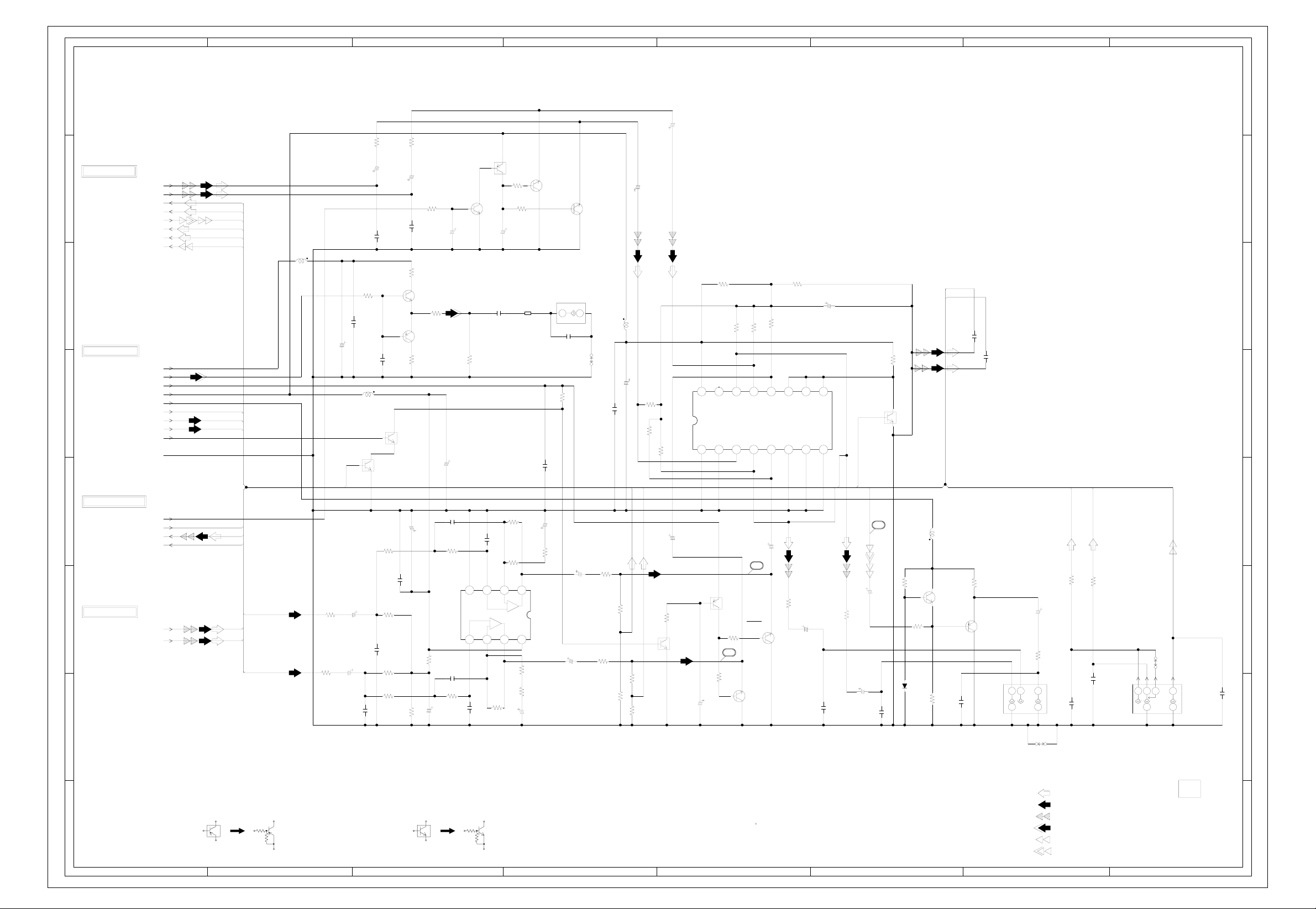
8
G-23
G-24
FROM/TO AV SW
7
6
5
FROM/TO MICON/TUNER
4
FROM SOUND AMP
3
2
MONITOR_AUDIO_L
MONITOR_AUDIO_R
FROM REGULATOR
ABC D E F GH
IN/OUT SCHEMATIC DIAGRAM
DVD_AUDIO_L
DVD_AUDIO_R
SWD_V_OUT
REAR_A_IN_L
REAR_A_IN_R
REAR_V_IN
P.CON+D5V
SPDIF-134
AT+5.6V
P.CON+12V
P.CON+9V
SYS_MUTE
DVD_A_OUT_L
DVD_A_OUT_R
ZERO
GND
EXT_MUTE
TV/DVD
AUDIO_OUT_R
AUDIO_OUT_L
SOUND_L+
SOUND_R+
DVD_A_OUT_L
DVD_A_OUT_R
L4202
100uH
KRC104SRTK
R4201
10K
R4202
10K
C4204
MUTE SW
Q4217
C4207
470
R4203
1016V KA
C4208_1
C4202
470P B
R4205
10 1/4W
C4205
0.022 B
476.3V KA
L4201 4.7mH 0607
3.2
SYS_MUTE
C4206
2.250V KA
2.250V
KA
C4210
1.6
1.6
C4209
100P CH
0
2.9
0
0
0
R4208
10K
R4211
100K
C4212
820P CH
R4212
100K
R4213
10K
820P CH
R4206
C4211_1
C4201
R4209
1.2
1.2
0
R4210
MUTE DET
Q4203
KRC104SRTK
C4217
0.1 B
C4216
R4219
470
1016V KA
KTC3875S_Y_RTK
R4214
10K 1/4W
470P B
10
4.9
D AUDIO DRIVER
Q4201
KTC3875S_Y_RTK
R4216
120
D AUDIO DRIVER
Q4202
KTA1504S_Y_RTK
10
C4203
0.0015 B
10016V KA
1K
R4218
0.0015 B
1K
3310V KA
C4214
MUTE SW
Q4204
7.3
0
0
1016V KA
C4213
56
R4221
10016V KA
C4220
R4224
10K
C4222
R4223
10K
C4226
5.2 5.2 5.2
0
A_GND
5678
5.2 5.2 5.2 10.4
C4225
100P CH
7.3
7.4
C4215
0.1 B
+
-
R4228
12K
0
C4219
100P CH
MUTE SW
Q4205
KRA102SRTK
R4225 2.2K
R4226
2.2K
4.750V KA
W4BRH3.5X6X1
R4229
12K
R4231
8.2K
1234
+
R4232
R4233
C4230
0.2
B4201
VCC
0.8
8.2K
1K
2.250V
MUTE SW
Q4207
KTC3875S_Y_RTK
0
0.2
MSP-251V-05PBSN
C4224
100P CH
R4243
C4233
220P CH
2.250V KA
C4229
1K
R4230
AMP IC
IC4201 NJM4580M
KA
1.1
COAXIAL
J4201
2
H
10K
C4232
2216V KA
KTC3875S_Y_RTK
0
1
E
W821
C4231
2216V KA
MUTE SW
Q4208
R4234
470
R4235
470
(AV PCB)
C4242_1
L4204
C4241
C4238
0.1 F
DVD_AUDIO_L
R4251
100 1/4W
R4252
10K
R4236
R4237
4.750V KA
100uH 0305
10016V YK
R4263
82K
R4264
DVD_AUDIO_R
100 1/4W
10K
82K
R4265
0
4.750V KA
C4243_1
10.9 5.4 5.4 5.4
IC4202
AUDIO SW IC
CD4053BNSR
82K
00 0 0
1016V KA
C4250
MUTE SW.
Q4210
KRA101SRTK
3.3K
R4238
5.2
MUTE SW.
Q4209
KRC103SRTK
0
C4234
R4269
82K
C4251
0
0
R4270
100K
82K
00
1011121314
AUDIO_OUT_L
1016V KA
120
R4242
C4277
0
MUTE SW
Q4211
KTC3875S_Y_RTK
0
1050V YK
R4266
100K
82K
R4268
R4267
NC
1516
BY BX CY COUT CX INH Vee Vss
2345678
1
5.4 5.4 5.4 0
39
5.2
5.2
0
4.750V KA
R4240
R4239
40
1K
0
1K
0
MUTE SW
Q4212
KTC3875S
Y_RTK
0
C4253_1
9
CBAAXAYAOUTBOUTVdd
C4239
1050V YK
AUDIO_OUT_R
R4241
470P B
SW
Q4213
KRC103SRTK
4.1
TV/DVD
SWD_V_OUT
C4252
120
C4276
1050V YK
41
1016V KA
C4237
R4227
0
0
470P B
10K
R4246
D4213
22K
R4247
100
1SS133
L4203
9.0
0.5
1.1
KTC3875S_Y_RTK
R4248
0305
100uH
BUFFER
Q4214
12K
SOUND_R+
SOUND_L+
1.8
1.1
C4249
C4274
470P CH
C4275
R4249
330 1/2W
KTA1504S_Y_RTK
0
100P CH
470P CH
BUFFER
Q4215
2345
J4202
1
REAR A/V OUT JACK
MSP-213V1-432_PBSN
C4240
R4250
EE
W898
REAR_A_IN_L
REAR_A_IN_R
R4262
R4271
100 1/4W
100 1/4W
10006.3V YK
68 1/4W
C4245
C4247
0.0022 B
J4203
0.0022 B
REAR A/V IN JACK
MSP-213V2-432_PBSN
H1H1 H2
REAR_V_IN
W807
H1NCH1H2
234
6
1
5
EE
C4265
8
7
6
5
4
3
100P CH
2
PCB250
AUDIO SIGNAL
CAUTION: DIGITAL TRANSISTOR
1
CAUTION: DIGITAL TRANSISTOR
NOTE:THIS SCHEMATIC DIAGRAM IS THE LATEST AT THE TIME
OF PRINTING AND SUBJECT TO CHANGE WITHOUT NOTICE
NOTE:THE DC VOLTAGE EACH PART WAS
MEASURED WITH THE DIGITAL TESTER
DURING PLAYBACK.
AUDIO SIGNAL(PB)
TUNER AUDIO SIGNAL
DIGITAL AUDIO SIGNAL(PB)
TMB543
1
TUNER VIDEO SIGNAL
PLAYBACK VIDEO SIGNAL
ABC D E F GH
Page 55

ABC D E F GH
G-25
G-26
AV SW SCHEMATIC DIAGRAM
8
(AV PCB)
8
C4280_1
4.3
L4206 1uH
220P B
R4217
1K
R4215
1K
C4228
2.250V KA
C4244
2.250V KA
9.0
5.0
R4284
220 1/4W
C4279
22P CH
C4246
0.1 B
C4278_1
R4220
100 1/4W
R4253
100 1/4W
R4254
270P B
100
R4255
100
R4256
100
W899
R4207
44
45
7
S902XS902Y
S901Y
S901X
6
30 31 32
Vcc
BIAS
GND
0
20 21 22 23 24 25 26 27 28 29
MUTE
19
0
SCL
SDA
17 18
AV SW IC
IC4203 MM1311AD
ADRESS
1K
R4275
110111213141516
2
3
456789
4.3
S1
S2
C4259
4.7
0.1 B
4.9
NC
4.4
4.9
NC
0
4.7
4.9
NC
4.4
4.9
NC
4.2
0
4.3
4.9
4.9
0
R4278
100
R4274
1K
C4261
C4262
2.250V KA
2.250V KA
R4279
100
C4263
0.1 B
C4264
C4256
2206.3V KA
2.250V KA
R4276
75 1/4W
C4267
2.250V KA
C4268
C4269
R4280
75
C4270
0.1 B
2.250V KA
2.250V KA
DVD_AUDIO_R
REAR_V_IN
REAR_A_IN_L
FRONT_VIDEO
5
4
3
10016V KA
C4255
4.9
4.3
4.9
NC
3.5
9.0
NC
3.5
4.3
43
5.0
4.2
4.2
100 1/4W
NC
4.4
NC
4.2
NC
4.3
3.9
R4257
100 1/4W
1K
R4259
7
C4221
FROM REGULATOR
6
FROM/TO MICON/TUNER
FROM STEREO
5
FROM/TO VIF/SIF/CHROMA
FROM/TO SOUND AMP
4
TO COMB FILTER
FROM/TO IN/OUT
3
GND
P.CON+9V
DVD_VIDEO
SWD_V_OUT
SDA
SCL
TU_AUDIO_L
TU_AUDIO_R
TU_VIDEO
MONITOR_VIDEO
MONITOR_AUDIO_L
MONITOR_AUDIO_R
FRONT_VIDEO
FRONT_AUDIO_L
FRONT_AUDIO_R
MONITOR_VIDEO
MONITOR_AUDIO_L
MONITOR_AUDIO_R
DVD_AUDIO_L
DVD_AUDIO_R
SWD_V_OUT
REAR_A_IN_L
REAR_A_IN_R
REAR_V_IN
C4218
0.0022 B
0.0022 B
L4205
100uH 0305
TU_AUDIO_L DVD_VIDEO
TU_VIDEO DVD_AUDIO_L
TU_AUDIO_R
C4223
0.01 B
C4227
2216V KA
BUFFER
Q4206
SWD_V_OUT
MONITOR_VIDEO
MONITOR_AUDIO_L
MONITOR_AUDIO_R
KTC3875S_Y_RTK
SCL REAR_A_IN_R
SDA
W915 (W211)
2
PCB250
TMB543
2
TUNER AUDIO SIGNAL
TUNER VIDEO SIGNAL
1
NOTE:THE DC VOLTAGE EACH PART WAS
MEASURED WITH THE DIGITAL TESTER
DURING PLAYBACK.
NOTE:THIS SCHEMATIC DIAGRAM IS THE LATEST AT THE TIME
OF PRINTING AND SUBJECT TO CHANGE WITHOUT NOTICE
PLAYBACK VIDEO SIGNAL
AUDIO SIGNAL
AUDIO SIGNAL(PB)
ABC D E F GH
1
Page 56
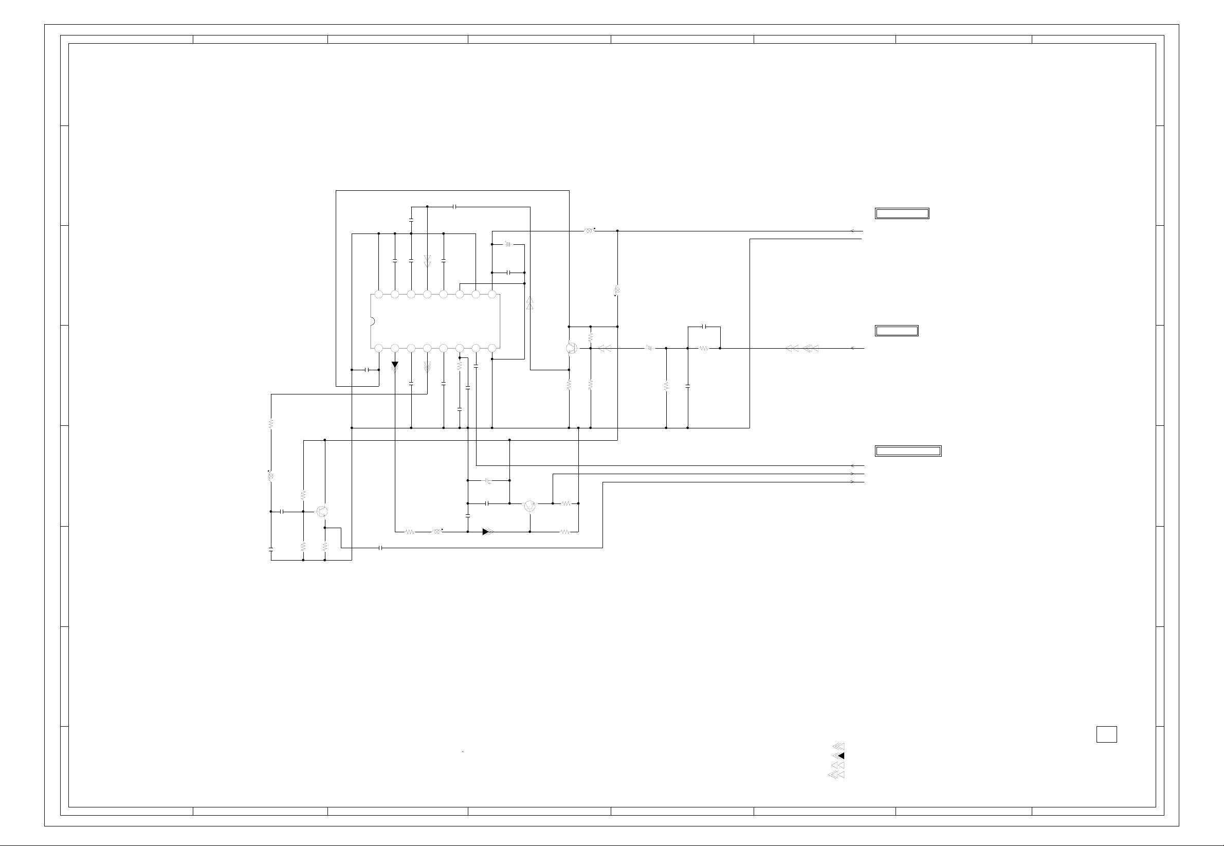
ABC D E F GH
G-27
G-28
COMB FILTER SCHEMATIC DIAGRAM
8
(AV PCB)
8
7
C1511
0.47 B
1.9 2.5
R15071KR1511
R1509
560
R1508
1.2K
L1503
820uH
R1510
5.4
L1504
150uH 0305
C1524
56K
27K
C1521_1
3.350V YK
R1512
56P CH
R1513
1K
330
C1523
39P CH
C1506
27P CH
C1518
2206.3V YK
C1505
C1507
6
IC1501 TC90A45F
DIGITAL COMB FILTER IC
1K
C1504
0.01 B
BUFFER
Q1501
KTC3875S_Y_RTK
5
330
R1501
4
L1501
C1501
15uH
C1502
0.1 B
56P CH
0305
R1502
R1503
5.0
6.8K
1.7
1.1
3.3K
R1504
0.01 B
1
2345678
SS
VRB
AV
DD
OUT
AV
Y
5.4 3.8 1.4 4.2 3.6 2.2 2.5 0
C1508
R1505
C1520
0.1 B
100
VRT
BIAS2
0.01 B
0.01 B
15uH 0305
ADIN
OUT
C
L1502
C1509
C1510
BIAS1
BIAS3
0.01 B
TEST
VFIL
820
R1506
0.01 B
C1513
0.01 B
C1512
C1514
10111213141516
C1515
180P CH
56P CH
KILLER
CKIN
00 2.4 3.0 2.6 2.6 0 5.5
9
100P CH
C1516
4716V YK
C1517
0.01 B
C1519
0.01 B
DD
DV
SS
DV
4.4 2.1
BUFFER
Q1502
KTC3875S_Y_RTK
BUFFER
Q1503
KTC3875S_Y_RTK
2.4
FROM REGULATOR
P.CON+5V
GND
FROM AV SW
MONITOR_VIDEO
FROM/TO VIF/SIF/CROMA
FSC
COMB_Y_OUT
COMB_C_OUT
7
6
5
4
3
2
PCB250
NOTE:THIS SCHEMATIC DIAGRAM IS THE LATEST AT THE TIME
OF PRINTING AND SUBJECT TO CHANGE WITHOUT NOTICE
1
NOTE:THE DC VOLTAGE EACH PART WAS
MEASURED WITH THE DIGITAL TESTER
DURING PLAYBACK.
RECORD COLOR SIGNAL
RECORD LUMINANCE SIGNAL
TUNER VIDEO SIGNAL
TMB543
3
2
1
PLAYBACK VIDEO SIGNAL
ABC D E F GH
Page 57

ABC D E F GH
G-29
G-30
STEREO SCHEMATIC DIAGRAM
8
7
6
R908
C920
0.1 B
5
C922
0.1 B
2.2 2.2 2.2 2.2 4.2 4.4 3.4 2.2
OUT SW
AGC
Matrix
De-Emph
75us
Cancel
Offset
Expand
Cancel
SOUN DECORDER IC
IC902 AN5829S
4
Wide Band
Offset
1 101112
3456789
2
1.0 2.2 2.3 2.4 0.7 5.1 2.6 2.6 0.6 2.2 3.62.2
(AV PCB)
C927
R909
470 1/4W
470 1/4W
NC
0 0 3.7
2021222324
DAC
ZAP
Switch
L-R Filter L-R Demod
(L-R)/SAP
Filter
SAPout
Wide Band
150P CH
IIC Decoder
fH.2fH Trap Filter
RMS Det
L+R DemodL+R Filter
dbx De-Emph
Vcc
C930
GND
150P CH
Cancel
Pilot
C933
St.PLL
Filter
Stereo
Filter
Wide Band
Expand
Spectral
8
7
FROM/TO MICON/TUNER
R911
100
R912
100
47
48
46
4.750V KA
C907
0.047 B
Det
Pilot
Filter
Spectral
RMS Det
Spectral
Filter
Noise
C938
0.1 B
13141516171819
VCA
Det
Input
SAP
Filter
SAP
Demod
SAP
Det
Noise
C935
2.7M
R913
0.1 B
3.4
SCL
SDA
TO AV SW
TU_AUDIO_L
TU_AUDIO_R
FROM VIF/SIF/CHROMA
SIF
6
5
4
C939
0.1 B
C925
4.750V KA
C926
4.750V KA
C928
C929
1016V KA
C934
0.1 B
C932
0.3350V KA
C937
C936
0.1 B
L902
100uH 0305
C931
1006.3V KA
3.350V KA
FROM REGULATOR
P.CON+5V
0.022 B
3
GND
2
PCB250
TMB543
NOTE:THIS SCHEMATIC DIAGRAM IS THE LATEST AT THE TIME
OF PRINTING AND SUBJECT TO CHANGE WITHOUT NOTICE
TUNER AUDIO SIGNAL
1
4.750V KA
R910
C921
220K
C923
C924
0.1 B
0.1 B
3
2
NOTE:THE DC VOLTAGE EACH PART WAS
1
MEASURED WITH THE DIGITAL TESTER
DURING PLAYBACK.
ABC D E F GH
Page 58
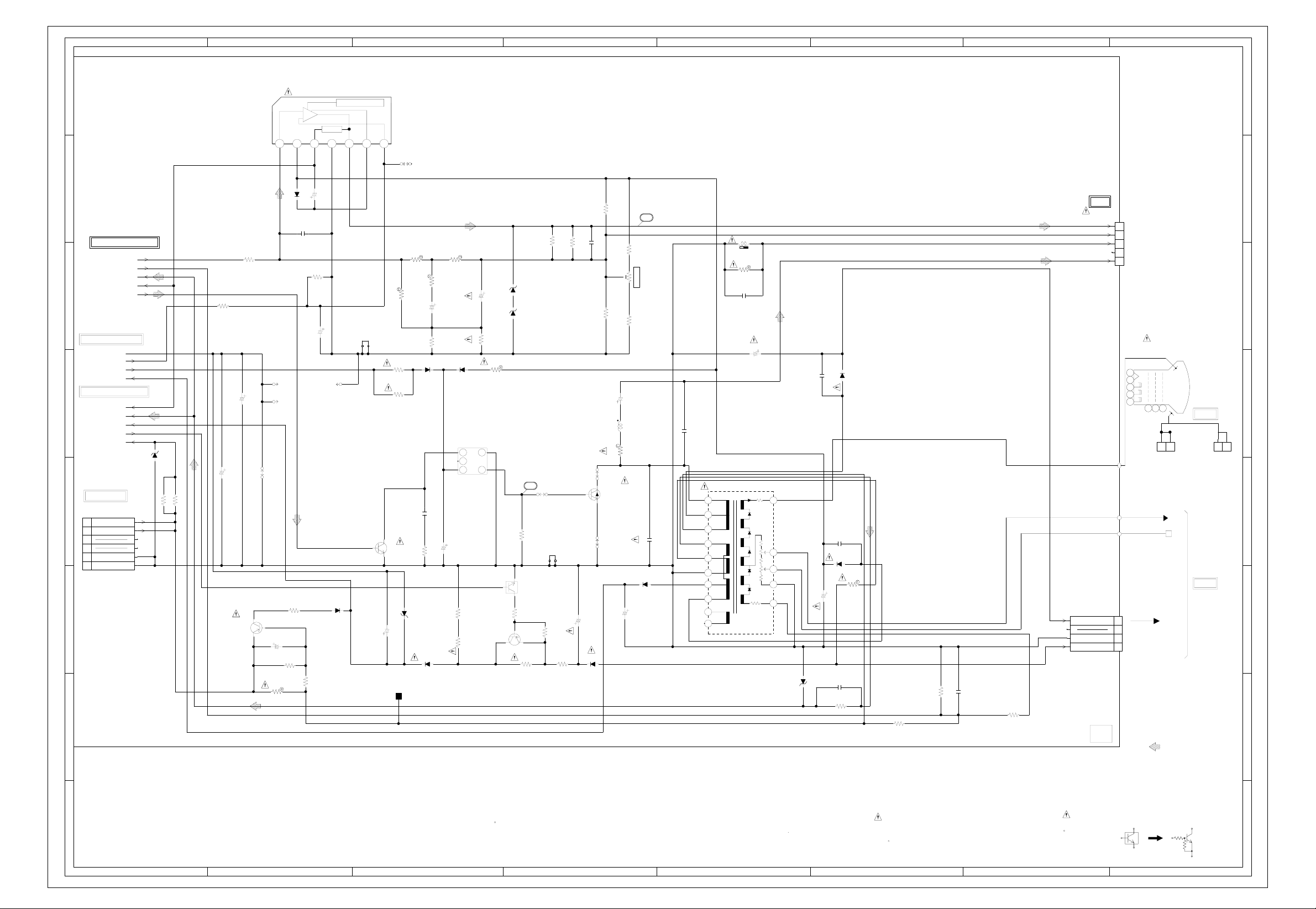
ABC D E F GH
G-31
G-32
8
7
6
FROM/TO REGULATOR
FROM/TO MICON/TUNER
5
FROM POWER
CP402
4
B2013H02-6P
1
2
3
4
5
6
3
2
FROM/TO VIF/SIF/CROMA
V.OUT
ACL
AFC
VD
H.OUT
GND
P.CON+5V
UNREG+12V
FBT+12V
VD
AFC
X-RAY
X_RAY_TEST
+30V
(CP3802)
+B
+B
H_GND
H_GND
NC
NC
D408
MTZJ33B
R405
R404 56K 1/2W
56K 1/2W
R424
1.2K 1/4W
C409
CURRENT DET.
C403_1
10035V MHE
Q401
2SA1624
8.2K
135.0
R412
IC401 LA78040V.OUTPUT IC
AMP
C406
11E1-EIC
R420
2.2K
5.6K 1/4W
PUMP UP
10035V YK
C404_1
150V MHE
S804YS804X
D414
11E1-EIC
THERMAL PROTECTION
+
Vcc GND
1234567
3.9 25.5 1.3 0 12.9 24.8 3.9
D401
C435
560P CH
S805X
4716V YK
W841
R409
22K 1/4W
0
135.0
C401_1
10250V MHE
R406
47K 1/4W
R408
R410
0.47 2W
HS401
763WAA0237
14.3
0
330 1/2W
330 1/2W
0
KTC3227_Y
C410
W843
R411
R401
R425
H-DRIVE
Q405_1
D416
1016V KA
TP401
NC
R413
27K +-1%
10K +-1%
1SS133
MTZJ5.1B
1SS133
R414_1
C405
R415
D406
C417_1
R456
D409
0.01100V MKT
470 1/2W
820 +-1%
0.4750V YK
1.8 1/2W
C418
R416
47K +-1%
D405
1SS133
ETH14Y47AY
31.0
NC
0.2
22.3
2250V YK
R446
R444
T401_1
45
3
560
5.6K +-1%
220025V MHE
C407
R418
1.5 1/2W
R402
270 2W
0
12
1.3
SWITHING
Q403
KRC111SRTK
SWITHING
Q404
KTA1266
DEFLECTION SCHEMATIC DIAGRAM
(AV PCB)
R421
R417
D403
MTZJ33B
D404
MTZJ33B
50
W809
R460
100 1/4W
HS402
763WSA0018
0
0
17.9
10K
R431
17.9
22K +-1%
17.910.0
R442
R428
10K
15K 1/4W
R445
390 1/2W
R419
C433
C411
390 1/2W
247.6
1.3
2250V YK
D412
RMPG06J
0.22100V MKT
R407
W823
0
W815
1.5K 1/2W
R463
1K 1/2W
R464
2.2250V MHE
C422
L401
4.7mH
R447
68 1/2W
H.OUTPUT
Q406_1
2SD2499
C402
470 1/2W
V.POSI
470 1/2W
0909
D415
10ELS6N
47016V YK
49
VR402
C428_3
METAL
1K
0.0121.25KV MPP
C423
0.39250V PMS
247.6
114.3
114.5
0
0
10
0
0
NC
FB401_3 3220056F
COL
1
E180
6
B+
2
AFC
9
HEA
TER
GND
8
E12
4
E27
3
GND
8
E8
5
L402
ELH5L4113
R448
1K 1W
C450
0.0012KV R
C431
22250V YK
ABL
GND
8
7
TO DY
CP401
A1561WV2-A5P
5
4
3
2
NC
1
6
V801
A51LXR195X80
0.001500V B
C430
D413
1N4937
HV
C429_1
C421
MTZJ6.8B
0.0022500V B
D411
1N4937
3.9 2W
47035V MHE
C439
56P500V SL
R423
12K 1/4W
R450
R453
82K 1/2W
R490
56K 1/4W
C432
0.1100V MKT
R430
5.6K 1/2W
180V
HEATER
CP803A
B2013H02-4P
NC
180V
GND
HEATER
PCB250
TMB543
F
S
11
0.8
7
D410
9
10
R
8
G
6
B
11
4
3
2
1
FOCUS
SCREEN
(CP803B)
175
21
CD805
CU823001
TO CRT
CU823001
TO CRT
5
12
CD801_1
4
3
2
DEFLECTION SIGNAL
NOTE:THE DC VOLTAGE AT EACH PART WAS MEASURED
1
WITH THE DIGITAL TESTER WHEN THE COLOR BROADCAST
WAS RECEIVED IN GOOD CONDITION AND PICTURE IS NORMAL.
ABC D E F GH
NOTE:THIS SCHEMATIC DIAGRAM IS THE LATEST AT THE TIME
OF PRINTING AND SUBJECT TO CHANGE WITHOUT NOTICE
THE RESISTOR MARKED F IS FUSE RESISTOR.NOTE:
THE ALUMI ELECTROLYTIC CAPACITOR MARKED NP
IS NON POLAR ONE.
DANGEREUSES AN POINT DE VUE SECURITE
N’UTILISER QUE CELLS DECRITES
DANS LA NOMENCLATURE DES PIECES
ETANTLES PIECES REPAREES PAR UNATTENTION:
CRITICAL FOR SAFETY,USE ONES
DESCRIBED IN PARTS LIST ONLY
ARESINCE THESE PARTS MARKED BYCAUTION:
CAUTION: DIGITAL TRANSISTOR
1
Page 59
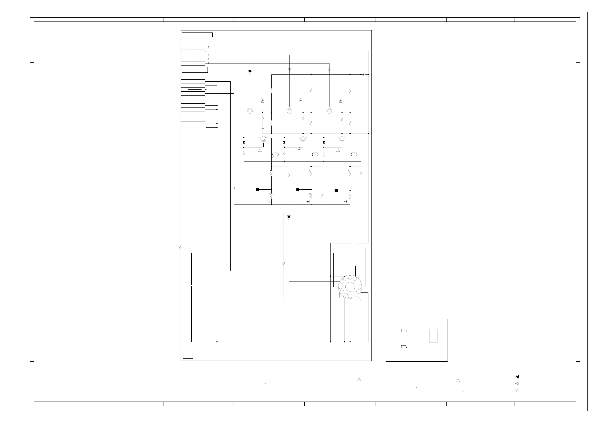
ABC DEF GH
G-33
G-34
8
7
6
5
FROM VIF/SIF/CHROMA
CP802B
(CP802A)
B2013H02-5P
1
CLAMP
2
GND
3
G.OUT
4
R.OUT
5
B.OUT
FROM DEFLECTION
CP803B
(CP803A)
B2013H02-4P
1
HEATER
2
GND
3
4
180V
CP801
A2361WV2-2P
1
GND
2
GND
CP805
(CD805)
A2361WV2-2P
1
GND
2
GND
C803
0.001
B
NC
3.2
100.6
2.7
D801
1SS133
220
R801
L801 150uH
R809
1.8K
RED AMP
Q801
2SC1740SP TP
560
R812
R813
C811
270P CH
2.6 2.5
3.0 2.9
RED AMP
Q804
KTC4217
L802_1
TP022
R803
3.2
98.4
330
D802
1SS133
51 52 53
220
R808
R802
150uH
2W
12K
2SC1740SP TP
2.7
1/4W
2.7K
GREEN AMP
Q803
R817
C810
GREEN AMP
Q805
KTC4217
TP023
122.0120.0
560
270P CH
R814
R816
L803_1
R807
1.8K
330
150uH
2W
12K
95.4
R806
D803
R810
3.2
1SS133
220
2.7K 1/4W
BLUE AMP
Q802
2SC1740SP TP
2.7
R818
C809
2.7
BLUE AMP
Q806
KTC4217
TP024
3.1
560
390P CH
115.0
R811
R815
L804_1
R805
1.8K
330
150uH
2W
12K
R804
2.7K 1/4W
CRT SCHEMATIC DIAGRAM
8
(CRT PCB)
7
6
5
4
C801_1
131.6
592
7
8
6
100PSL
0
10
9
5
4
CRT SOCKET
CVT3275-5101
135.5
11
J801_2
F
1
ACCESSORY
BT002
R03(AB)E_20_T
UM4
BT001
R03(AB)E_20_T
UM4
ARESINCE THESE PARTS MARKED BYCAUTION:
DANGEREUSES AN POINT DE VUE SECURITE
N’UTILISER QUE CELLS DECRITES
DANS LA NOMENCLATURE DES PIECES
TM101
TOT201N09080
ETANTLES PIECES REPAREES PAR UNATTENTION:
R.SIGNAL
G.SIGNAL
B.SIGNAL
FOCUS
3
C802
0.0012KV B
133.0
2
PCB110
TCB402
1
NOTE:THE DC VOLTAGE AT EACH PART WAS MEASURED
WITH THE DIGITAL TESTER WHEN THE COLOR BROADCAST
WAS RECEIVED IN GOOD CONDITION AND PICTURE IS NORMAL.
NOTE:THIS SCHEMATIC DIAGRAM IS THE LATEST AT THE TIME
OF PRINTING AND SUBJECT TO CHANGE WITHOUT NOTICE
CRITICAL FOR SAFETY,USE ONES
DESCRIBED IN PARTS LIST ONLY
4
3
2
1
ABC DEF GH
Page 60

ABC D E F GH
G-35
G-36
8
7
6
5
4
3
2
AC120V_60Hz
CD3800
0R414903
DEGAUSS COIL
L3800
8R200024
L3803
HF70T22*10*14
WIDE
MLADE
WHITE
BLACK
21
CP3800
A1561WV2-2P
1
2
S3802
WHITE
S3801
BLACK
+B ADJ
FH3800
EYF-52BC
METAL
VR3800470
R3800
ZPB45BL3R0A
F3800
5A125V
51MS050LCC
5A 125V
3K +-1%
TH3800_1
FH3801
EYF-52BC
C3800
0.001 B
FEED BACK
SWITCHING
R3801
R3802
003P-2100
Q3800
KTC3198
2.2K 1/4W
56K 1/2W
RY3800
ALKS321
(LKS1af-12V)
PH3800
1
PHE840
0.22
C3801
275V
6.3
6.0
5.4
D3801
3
R3803_1
R3804
R3805
MTZJ5.6B
D3802
1SS133
1.5M 1/2W
330 1/4W
1K 1/4W
0.2
0
12
4
R3806
34
12
COIL,LINE FILTER
L3801
2R2A752F28
C3802
7.3
6.3
0.6
RELAY DRIVE
Q3801
KTC3198
+-10%
2.7M 1/2W
KX
0.001
250V
1
2
FEED BACK
LTV-817M-VB
13.6
0.4
34
IC3800
BUFFER
Q3802
KTC3203_Y
C3804
W809
0.1275V PHE840
POWER SCHEMATIC DIAGRAM
(POWER PCB)
8
TO DEFLECTION
CP3802
(CP402)
52147-0610
+B
+B
NC
NC
H_GND
H_GND
FROM/TO REGULATOR
CP3803
(CP8004)
52147-1010
SOUND_GND
SOUND+B
DEGAUSS-H
NC
POWER_FAIL
UNREG+5V
UNREG+8V
UNREG+12V
GND
GND
1
2
3
4
5
6
7
6
5
10
9
8
7
6
5
4
3
2
1
4
R3807
C3803
10K 1/4W
0.001250V KX
W802
10K 1/4W
(1000PF)
R3808
R3812
60
330 1W
R3817
17W
R3816
270 1/4W
C3807_1
0.047100V MMTV
W804
POWER
Q3803
2SK3326(2)
C3814
0.001 B
R3833
330 1/4W
D3808
D3809
D3810
6.3
RM11C-EIC
C3810
0.0012KV
RM11C-EIC
MTZJ18B
356
D
G
S
0
R3821
B
0.15 1W
D3806
1SS133
C3812
0.0012KV B
R3826
1.2M 1/4W
0.00152KV R
C3811
763WAA0166
D3815
RM11C-EIC
D3816
RM11C-EIC
R3827
1.2M 1/4W
B3800
W4BRH3.5X6X1.0X2
HS3800
C3815
R3828
0.22 1W
470200V UP
T3800_1
81350824
138.0
89
P2
7
6
P1
320.0
5
7.8
3
P4
0
2
P3
13.3
1
135V
12V
4.1
5V
8.7
SB
10
0
SG
11
135.0
12
HG
13
0
LG
14
14.2
15
8.2
8V
16
B3801
W5RH3.5X5X1.0
D3818
1N4937
D3817
SB340L-6737
61
R3829
100 1/4W
C3818
D3819
21DQ09N
D3830
21DQ09N
D3823
SB290S
D3824
SB290S
D3821
RU2AM-EIC
C3824_2
470P2KV RR
C3820_1
100016V MHE
D3820
SB290S
R3830
1K 1/4W
10100V MHE
C3822
C3823
220016V MHE
100025V MHE
C3826
D3825
MTZJ11B
C3827
MHE
2200
16V
TP3801
220200V YXF
TP3802
R3819
100 1/4W
3
0.01 B
C3805
D3807
1N4937
6.3
0.4
0
W805
D3804
C3806
MTZJ18B
0.01 B
C3808_1
4725V MHE
R3832
1K 1/2W
IS THE LIVE CONNECTIONCAUTION:
R3825
10 1/2W
C3816
0.0022250V KX
(2200PF)
R3813
100 1/4W
D3831
MTZJ5.1B
D3822
1SS133
R3831
100 1/4W
D3826
D3827
1SS133
D3828 MTZJ3.9B
1SS133
D3829
1SS133
PCB020
VPB157
2
5A 125V
1
ATTENTION:POUR UNE PROTECTION CONTINUE LES RISQUES D’INCEIE
N’UTOLISER QUE DES FUSIBLE DE MEME TYPE
CAUTION:FOR CONTINUED PROTECTION AGAINST FIRE HAZARD,
REPLACE ONLY WITH THE SAME TYPE FUSE
ABC D E F GH
5A 125V(F3800).
5A 125V(F3800).
NOTE:THIS SCHEMATIC DIAGRAM IS THE LATEST AT THE TIME
OF PRINTING AND SUBJECT TO CHANGE WITHOUT NOTICE
NOTE:THE DC VOLTAGE AT EACH PART WAS MEASURED
WITH THE DIGITAL TESTER WHEN THE COLOR BROADCAST
WAS RECEIVED IN GOOD CONDITION AND PICTURE IS NORMAL.
THE RESISTOR MARKED F IS FUSE RESISTOR.NOTE:
THE ALUMI ELECTROLYTIC CAPACITOR MARKED NP
IS NON POLAR ONE.
CRITICAL FOR SAFETY,USE ONES
DESCRIBED IN PARTS LIST ONLY
ARESINCE THESE PARTS MARKED BYCAUTION:
DANGEREUSES AN POINT DE VUE SECURITE
N’UTILISER QUE CELLS DECRITES
DANS LA NOMENCLATURE DES PIECES
ETANTLES PIECES REPAREES PAR UNATTENTION:
1
Page 61

ABC D E F GH
G-37
G-38
OPERATION SCHEMATIC DIAGRAM
8
7
FROM/TO MICON/TUNER
CD757_1
(CP102)
CU292501
1
REMOCON_OUT
2
6
5
3
4
POWER_ON_LED
5
6
7
8
9
GND
AT+5V
KEY_A
KEY_B
NC
NC
NC
D752
MTZJ6.8B
C781
C779A
0.001 B
POWER ON/OFF
0.001 B
CH DOWN
SW751_1
SW799
R778
820 1/4W
EVQ21505R
R775A
820 1/4W
EVQ21505R
SW795
EVQ21505R
REC/OTR(OPEN)
SW798
CH UP
R771
1K 1/4W
R776
1K 1/4W
EVQ21505R
SW791
STOP/EJECT
VOL UP
R772
1.5K 1/4W
EVQ21505R
SW796
EVQ21505R
PLAY
SW792
R777
1.5K 1/4W
R773A
2.7K 1/4W
EVQ21505R
SW797
VOL DOWN
(OPERATION PCB)
R774
5.6K 1/4W
SW793
FF/CUE(SKIP FF)
EVQ21505R
EVQ21505R
SW794
EVQ21505R
REW(SKIP REW)
C755A
8
7
6
R766
100 1/2W
2206.3V KA
C751A
0
3
GND
4.8
2
B+
4.8
Vout
1
OS753
PIC-28143TC5
100P B
D792
POWER
R761A
270 1/4W
POWER LED SW
LTL-1CHEE-002A
KRC114MAT
Q752A
0
5.0
0
5
C704_1
4
FROM/TO SOUND AMP
CD702
(CP303)
CU2B2801
1
FRONT_VIDEO_IN
GND
2
3
FRONT_AUDIO_IN_L
4
SOUND_GND
5
SOUND_OUT_L
6
3
SPEAKER
SP351
SG04H02BRA
8OHM
SPEAKER
SP352
SG04H02BRA
2
1
8OHM
NOTE:THE DC VOLTAGE AT EACH PART WAS MEASURED
WITH THE DIGITAL TESTER WHEN THE COLOR BROADCAST
WAS RECEIVED IN GOOD CONDITION AND PICTURE IS NORMAL.
SP_OUT_L
GND
7
8
FRONT_A_IN_R
9
10
SOUND_OUT_R
11
SP_OUT_R
CD355 CU123802
SP OUT R+
1
SP OUT R-
2
CD356 CU123802
SP OUT L+
1
SP OUT L-
2
NC
W809
W806
W808
W812
C352B
10016V YK
NOTE:THIS SCHEMATIC DIAGRAM IS THE LATEST AT THE TIME
OF PRINTING AND SUBJECT TO CHANGE WITHOUT NOTICE
C353
4716V KA
C351
4716V KA
R351
120 1/2W
120 1/2W
W813
R352
HEADPHONE JACK
J351
HTJ-035-28A
1
5
4
3
2
6
7
CRITICAL FOR SAFETY,USE ONES
DESCRIBED IN PARTS LIST ONLY
FRONT AV JACK
JPJ1187-010010
W804
100P CH
J701_1
H
2
H
4
H
6
7
NC
C702
0.001 B
C701
0.001 B
E
1
E
3
E
5
AUDIO SIGNAL
PCB030
TEXA33
AUDIO SIGNAL(PB)
TUNER AUDIO SIGNAL
TUNER VIDEO SIGNAL
ARESINCE THESE PARTS MARKED BYCAUTION:
DANGEREUSES AN POINT DE VUE SECURITE
N’UTILISER QUE CELLS DECRITES
DANS LA NOMENCLATURE DES PIECES
ETANTLES PIECES REPAREES PAR UNATTENTION:
CAUTION: DIGITAL TRANSISTOR
4
3
2
1
ABC D E F GH
Page 62
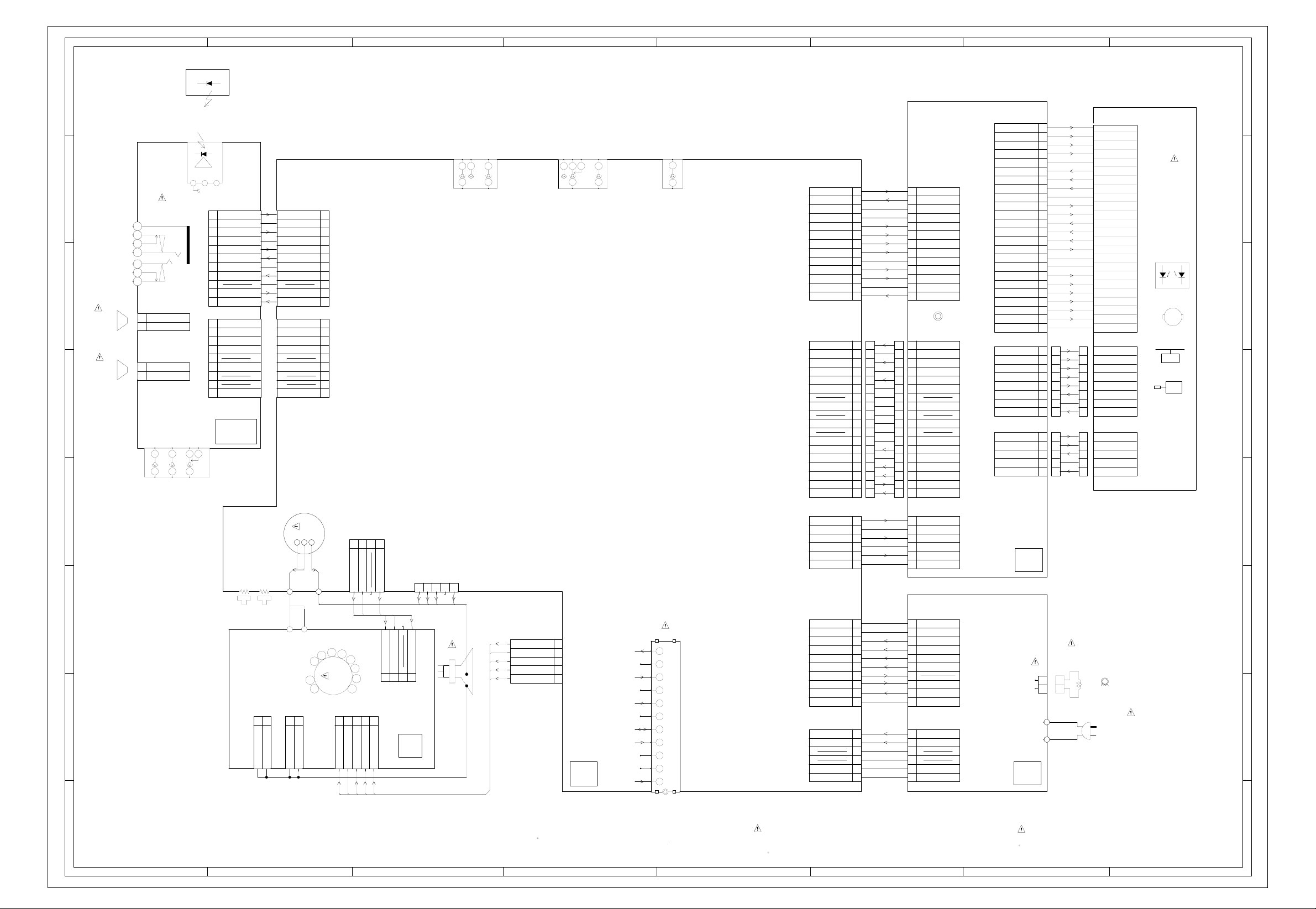
ABC DEF GH
G-39
G-40
INTERCONNECTION DIAGRAM
8
7
HEADPHONE JACK
1
5
4
3
2
6
7
6
SPEAKER
L CH
SPEAKER
R CH
CD355
2
1
CD356
2
1
8 OHM
SP351
8 OHM
SP352
5
4
3
2
COMMAND TRANSMITTER
REMOCON SENSOR
J351
SP_OUT_R-
SP_OUT_R+
SP_OUT_L-
SP_OUT_L+
FRONT AV JACK
J701_1
4
123
TM101
OS753
H
6
5
EHEHE
TO
GND
3
OS753
7
B+
2
NC
TM101
FROM
1
2
3
4
5
6
7
8
9
10
11
CD757_1
1
2
3
4
5
6
7
8
9
V.OUT
1
FRONT_VIDEO_IN
GND
FRONT_A_IN_L
GND/SOUND GND
SOUND_OUT_L
SP_OUT_L
GND
FRONT_A_IN_R
SOUND_OUT_R
SP_OUT_R
REMOCON OUT
GND
AT+5.6V
POWER ON LED
KEY A
KEY B
OPERATION PCB
PCB030
TEXA33
FOCUSSCREEN
1
CP801
GND
CD801_1
FRONT_VIDEO_IN
FRONT_A_IN_L
GND/SOUND GND
SOUND_OUT_L
FRONT_A_IN_R
SOUND_OUT_R
POWER ON LED
CP806_1
2
CP805
GND
GND
SP_OUT_L
GND
SP_OUT_R
REMOCON OUT
GND
AT+5.6V
KEY A
KEY B
FBT
FB401_3
FOCUS
SCREEN
1
1
2
GND
GND
CD805
CP303CD702
CP102
4F
1
2
3
4
5
6
7
8
9
10
11
1
2
3
4
5
6
7
8
9
5
CP802B
CP803A
6
7
8
J801_2
CRT SOCKET
11
12345
GND
CLAMP
1
HEATER
CD803
9
10
G.OUT
2
GND
R.OUT
CP2601
CD2601
24
F-
23
F+
22
T+
21
H1H1 H2
2 345
1
EE
REAR A/V OUT JACK
J4202
3
4
180V
CP401
NC
NC
CP803B
GND
HEATER
1
2
3
4
CRT PCB
PCB110
B.OUT
TCB402
180V
234
5
1
NC
V801
ANODE
H.V
CRT
CP802A
CLAMP
GND
G.OUT
R.OUT
B.OUT
1
2
3
4
5
H1NCH1H2
2 34
6
1
5
EE
REAR A/V IN JACK
J4203
AV PCB
PCB250
TMB543
H
2
1
E
COAXIAL
J4201
TU001
14 15
IF
11
NC
10
BTL
9
NC
8
BPL
7
V.S
6
NC
SDA
5
SCL
4
NC
ADRES
3
NC
2
AGC
1
12 13
CP8001
1
TX
2
RX
3
GND
4
GND
5
P.CON+9V
6
P.CON+9V
P.CON+D5V
P.CON+D5V
P.CON+3.3V
P.CON+3.3V
SPDIF-134
P.CON+5V_A P.CON+5V_A
MOTOR_GND MOTOR_GND
UNREG+12V
UNREG+8V
UNREG+5V
POWER FAIL
SOUND_GND SOUND_GND
7
8
9
GND
10
11
12
GND
13
CP8002
Y(G)
1
CP8005
CP8004
CP402
1
2
2
3
3
4
4
5
5
6
6
7
7
8
8
9
9
10
10
11
11
12
12
13
13
14
14
15
15
16
16
17
17
18
18
1
2
3
4
5
6
1
2
3
4
5
6
7
8
9
10
1
2
3
4
5
6
GND
C(CVBS)
GND
CVBS
GND
GND
GND
GND
AUDIO-L
GND
AUDIO-R
ZERO
DVD_RESET
SYS_MUTE
P.CON+5V P.CON+5V
GND
GND
GND
GND
STANDBY-H
DEGAUSS_H DEGAUSS_H
SOUND+B
+B
+B
H_GND
H_GND
CD8002
FFC
CD8501
TX
1
RX
2
GND
3
GND
4
P.CON+9V
5
P.CON+9V
6
P.CON+D5V
7
P.CON+D5V
8
GND
9
P.CON+3.3V
10
P.CON+3.3V
11
GND
12
13
SPDIF-134
L8507
CP8502
18
17
16
15
14
13
12
11
10
9
8
7
6
5
4
3
2
1
CD8502
1
2
3
4
5
6
CP3803
1
2
3
4
5
6
7
8
9
10
CP3802
1
2
3
4
5
6
Y(G)
GND
C(CVBS)
GND
CVBS
GND
GND
GND
GND
AUDIO-L
GND
AUDIO-R
ZERO
DVD_RESET
SYS_MUTE
GND
GND
P.CON+9V_AP.CON+9V_A
GND
GND
UNREG+12V
UNREG+8V
UNREG+5V
POWER_FAIL
SOUND+B
+B
+B
H_GND
H_GND
18
17
16
15
14
13
12
11
10
9
8
7
6
5
4
3
2
1
T-
20
(NC)
19
B
18
A
17
E
16
GND-PD
15
VC
14
VCC
13
F
12
D
11
C
10
CD/DVD
9
(NC)
8
(NC) (NC)
7
VR-CD
6
VR-DVD
5
MD
4
LD-CD
3
HFM
2
LD-DVD
1
GND-LD
SLD1
SLD2
SP1+
SP1-
+5V
SP_FG
GND
MLD1(-) MLD1(-)
MLD2(+)
CLOSE
GND(D)
OPEN
DVD PCB
PCB130
VMB261
CP3800
POWER PCB
PCB020
VPB157
CP2301
CP2302
S3802
S3801
1
2
3
4
5
6
7
8
1
2
3
4
5
1
2
CD2301
FFC
1
2
3
4
5
6
7
8
CD2302
FFC
1
2
3
4
5
DEGAUSS COIL
L3800
21
WHITE
BLACK
F-
F+
T+
T-
(NC)
B
A
E
GND-PD
VC
VCC
F
D
C
CD/DVD
(NC)
VR-CD
VR-DVD
MD
LD-CD
HFM
LD-DVD
GND-LD
SLD1
1
SLD2
2
SP1+
3
SP1-
4
+5V
5
SP_FG
6
7
GND
LIMIT_SWLIMIT_SW
8
1
MLD2(+)
2
CLOSE
3
GND(D)
4
OPEN
5
L3803
BLADE
WIDE
AC120V_60Hz
CD3800
DVD
DRIVE
OPTICAL PICK-UP
LOADING MOTOR
LM
SPINDLE MOTOR
SLED MOTOR
8
7
6
5
4
3
2
1
OF PRINTING AND SUBJECT TO CHANGE WITHOUT NOTICE
THE TIMETHIS INTERCONNECTION DIAGRAM IS THE LATEST ATNOTE:
DANGEREUSES AN POINT DE VUE SECURITE
N’UTILISER QUE CELLS DECRITES
DANS LA NOMENCLATURE DES PIECES
ETANTLES PIECES REPAREES PAR UNATTENTION:
CRITICAL FOR SAFETY,USE ONES
DESCRIBED IN PARTS LIST ONLY
ARESINCE THESE PARTS MARKED BYCAUTION:
1
ABC DEF GH
Page 63
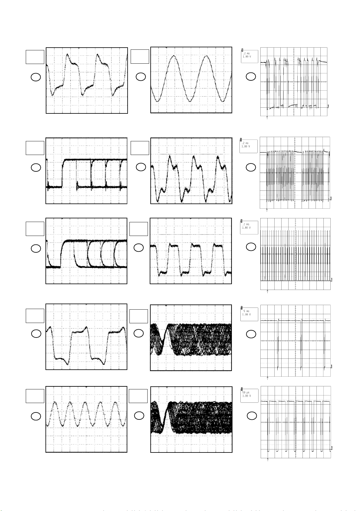
WAVEFORMS
MPEG
10ns
1.0V
1
100ns
1.0V
2
SYSCON1
20ns
500mV
6
DSP
20ns
1.0V
7
MICON/TUNER
22
23
100ns
1.0V
3
1ms
1.0V
4
MEMORY
5ns
1.0V
20ns
1.0V
8
READ CHANNEL
200ns
200mV
9
200ns
200mV
24
25
5
10
NOTE:
The following waveforms were measured at the point of the corresponding
balloon number in the schematic diagram.
26
H-1
Page 64

VIF/SIF/CHROMA
WAVEFORMS
21
27
28
31
32
33
36
SOUND AMP
37
38
29
30
34
35
NOTE:
IN/OUT
39
40
The following waveforms were measured at the point of the corresponding
balloon number in the schematic diagram.
H-2
Page 65

WAVEFORMS
41
AV SW
43
44
47
48
DEFLECTION
49
52
53
TV POWER
60
45
STEREO
46
50
CRT
51
NOTE:
61
The following waveforms were measured at the point of the corresponding
balloon number in the schematic diagram.
H-3
Page 66

TOSHIBA VIDEO PRODUCTS PTE. LTD.
438B ALEXANDRA ROAD, BLOCK B #06-01 ALEXANDRA TECHNOPARK SINGAPORE 119968
 Loading...