

Page 1
SERVICE MANUAL
8M266 CHASSIS
Design and specifications are subject to change without prior notice.
(Only Referrence)
SIZE:A5
Description:
MODEL.
JOB NO.
Engineering Dept:
Artwork By:
Checked By:
Approved By:
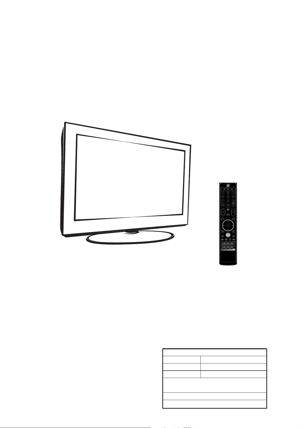
SERVICE MANUAL 8M26S
Brand Name:
SKYWORTH
Date:
Date:
Date:
2011-8-10
Page 2
Content--------------------------------------------------------------2
11-17
18
19-20
21-28
29-45
46-49
50-57
Page 3
LED 8M26S
Page 4
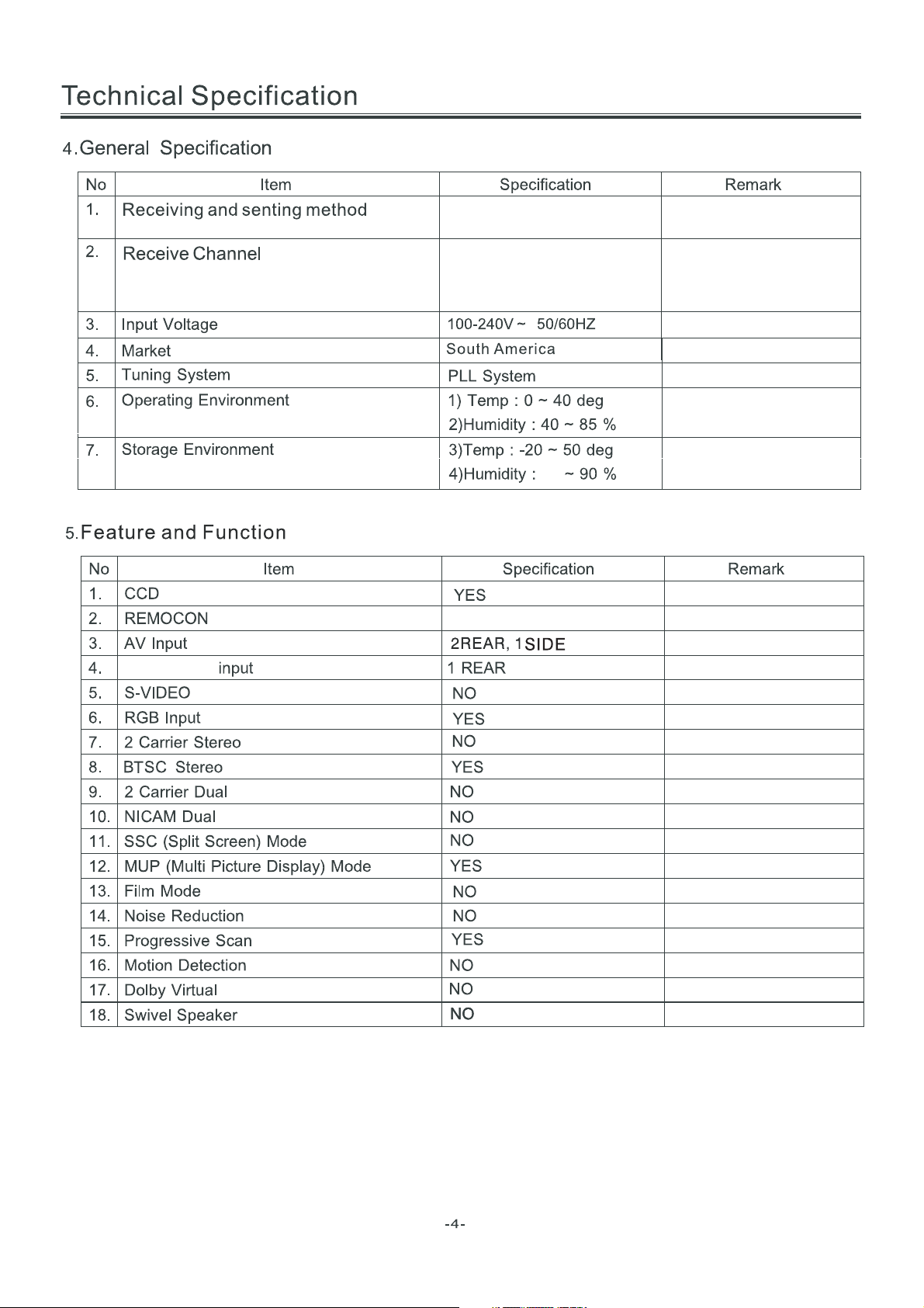
NTSC-M PAL-M PAL-N
Component
VHF LOW 2~B
VHF HIGH C~W+11
VHF W+12~69
TOSHIBA CODE
55.25MHz ~ 127.25MHz
133.25MHz ~ 311.25MHz
367MHz ~ 801.25MHz
Page 5
40
55
80
For 22” LED
For 24” LED
For 32” LED
Page 6
(24 inches is 4 ohm)
(24 inches is 3W)
Page 7
80
(26inches is 8 ohm)
40
40
3
2
1
4.2
50
0.5
12000
40
3
Page 8
Standard
Standard
20
40
NO
YES
8
6
46
46
NO
Spanish
Page 9
4
2
4
0 40 7 0
0 40 7 0
0 40
40 85
-Y 0 5 0
30000
Page 10
D
C
B
P12
SPEAKER
1
EARPHONE
TU2
TUNER
1
U29
U42
FLASH
2
M13S2561616A-5TG2K ESMT
U7 U1
TPA1517NE
SDA
SCL
P7
S/PDIP
2
3
4
LVDS OUT
U10
MST6E181VS
BH3544F-E2 TPA3113D2/
U19
PS331TQFP64G
P13
2P3P1P
P6
AV OUT
YPbPr AV2 INHDMI 1 VGA
PC
AUDIO
HDMI 2
3
4
MEDIA 2
5
AV1 IN
CON11
C
B
A A
D
CON10
CON6 MEDIA 1
5
Page 11
IC Block Diagram
U20 U23 U31(3.3V/1A 3-TERMINAL POSITIVE VOL TAGEREGULATOR) LD1117-3.3 SOT-223
-
8᧤9$/2:'523287/,1($5$55(*8/$725᧥/'$'-72
Thermal
Protection
A1
B
A2
For Adjustable Output, disconnect A1 and A2, connect B
For Fixed Output, connect A1 and A2, disconnect B
-
+
3
2
1
INPUT
OUTPUT
ADJ/
GND
-11-
Page 12
U28˄1A 3.3V SOT-223˅AS1117L-ADJ
U6 ˄(1MHZ,800MA SYNCHRONOUS STEP-DOWN CONVERTER˅MP2105DJ TSOT23-5
-12-
Page 13
IC Block Diagram
U10(LCDTV CONTROLLER WITH VIDEO ECODE)MST6E181VS
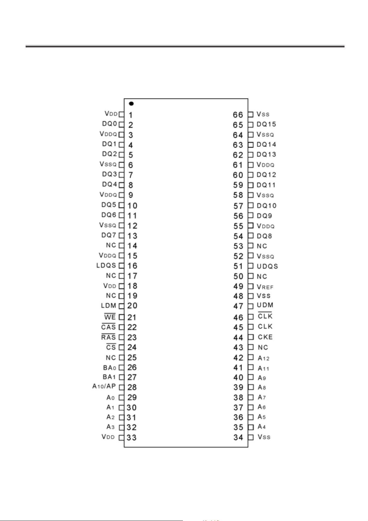
PIN DIAGRAM (MST6E181VS)
162
161
160
159
158
157
156
155
154
153
152
151
150
149
148
147
146
145
144
143
142
141
140
139
138
137
136
135
134
133
132
131
130
129
NC
NC
LDQS0
LDQM0
A_DDR1_BA0
DVDD_DDR_1.2V
A_DDR1_DQ8
A_DDR1_DQ9
AVDDIO_2.5V
A_DDR1_DQ10
A_DDR1_DQ11
A_DDR1_DQ12
A_DDR1_DQ13
A_DDR1_DQ14
AVDDIO_2.5V
A_DDR1_DQ15
A_DDR1_MCLKZ
AVDDIO_2.5V
A_DDR1_MCLK
A_DDR1_CKE
A_DDR1_A12
A_DDR1_A11
A_DDR1_A9
AVDDIO_2.5V
A_DDR1_A8
A_DDR1_A7
A_DDR1_A6
A_DDR1_A5
A_DDR1_A4
AVDD_NODIE
DVDD_NODIE
GND_EFUSE
GPIO11/SAR0
GPIO12/SAR1
GPIO13/SAR2
GPIO10/PMGPIO
GPIO6/PM1/TX
GPIO8/PM5/RX
GPIO9/PM6/CS1
AVDDIO_2.5V
GPIO7/PM4/POWER_ON
163
164
165
166
167
168
169
170
171
172
173
174
175
176
177
178
179
180
181
182
183
184
185
186
187
188
189
190
191
192
193
194
195
196
197
198
199
200
201
202
203
204
205
206
207
208
209
210
211
212
213
214
215
216
217
AVDD_PLL
UDQM0
UDQS0
A_MVREF
NC
VDDC
DDCR_DA
VDDP_3
DDCR_CK
TESTPIN
DM_P0
DP_P0
DM_P1
DP_P1
SPI_CK
SPI_DI
SPI_DO
SPI_CZ
DDCA_CK
DDCA_DA
E-pad
AVDDIO_2.5V
A_DDR1_DQ4
A_DDR1_DQ7
A_DDR1_DQ6
A_DDR1_DQ5
AVDDIO_2.5V
A_DDR1_DQ3
A_DDR1_DQ2
A_DDR1_DQ1
A_DDR1_DQ0
AVDDIO_2.5V
A_DDR1_CAS
A_DDR1_RAS
A_DDR1_WEZ
A_DDR1_BA1
A_DDR1_A0
A_DDR1_A1
A_DDR1_A2
A_DDR1_A3
A_DDR1_A10
NC
NC
VDDC
VDDP_2
GPIO21/PWM1
GPIO20/PWM0
GPIO77/I2S_OUT_MUTE/PWM3/LVSYNC
MST6E181VS
128
127
126
125
124
123
122
121
120
119
118
117
116
115
VDDC
AVDD_LPLL
R_ODD7/RXO0-
R_ODD5/RXO1-
AVDD2P5_MOD
GPIO75/I2S_IN_SD/PWM5/TX3/LDE
GPIO74/I2S_IN_WS/PWM4/RX3/LCK
GPIO76/I2S_IN_BCK/PWM2/LHSYNC
R_ODD3/RXO2-
R_ODD1/RXOC-
R_ODD6/RXO0+
R_ODD4/RXO1+
R_ODD2/RXO2+
114
113
112
111
110
109
G_ODD3/RXE0-
G_ODD7/RXO3-
G_ODD5/RXO4-
G_ODD6/RXO3+
G_ODD4/RXO4+
R_ODD0/RXOC+
G_ODD2/RXE0+
AVDD2P5_MOD
108
G_ODD1/RXE1-
107
G_ODD0/RXE1+
106
B_ODD7/RXE2-
105
B_ODD6/RXE2+
104
B_ODD5/RXEC-
103
B_ODD4/RXEC+
102
B_ODD3/RXE3-
101
B_ODD2/RXE3+
100
B_ODD1/RXE4-
99
B_ODD0/RXE4+
98
NC
97
GPIO49
96
GPIO47
95
GPIO45
94
GPIO38
93
GPIO37
92
GPIO36
91
GPIO32/I2S_OUT_BCK
90
GPIO30/I2S_OUT_MCK
89
GPIO28
88
VDDP_1
87
VDDC
86
GPIO27/SPDIF_OUT
85
GPIO26/SPDIF_IN/RX1/PWM3
84
GPIO25/TUNER_SDA
83
GPIO24/TUNER_SCL
82
GPIO23/I2S_OUT_SD/TX2
81
GPIO22/I2S_OUT_WS/RX2
80
TAGC
79
SIFM
78
SIFP
77
AVDD25_PGA
76
VIFP
75
VIFM
74
AVSS_PGA
73
AVDD25_REF
72
AVDD_DMPLL
71
XTAL_OUT
70
XTAL_IN
69
NC
68
NC
67
NC
66
LINEOUT_R0
65
LINEOUT_L0
64
LINEOUT_R3
63
LINEOUT_L3
62
AVDD_AU33
61
LINEIN_R5
60
LINEIN_L5
59
LINEIN_R4
58
LINEIN_L4
57
LINEIN_R3
56
LINEIN_L3
55
U?
IRIN
2
1
9876543
10
RX1N
AVDD_DVI_3.3V
RX0P
RX0N
RXCP
RXCN
HOTPLUGA
RESET
CEC
HSYNC0
VDDC
NC
NC
SOGIN0
BIN0P
2726252423222120191817161514131211
GIN0M
GIN0P
VSYNC0
RIN0P
SOGIN1
BIN1P
AVDD2P5_ADC
AVDD1P2
GIN1M
GIN1P
CVBS3
CVBS4
AVDD3P3_ADC
RIN1P
CVBS1
CVBS2
CVBS0
4443424140393837363534333231302928
45
CVBS_OUT1
VCOM
LINEIN_L0
LINEIN_R1
LINEIN_L1
LINEIN_R0
VRM
VRP
VAG
545352515049484746
AVDD_AU25
NCNCNCNCNC
ARC
DDCDA_CK
RX2P
RX2N
DDCDA_DA
RX1P
-13-
Page 14
IC Block Diagram
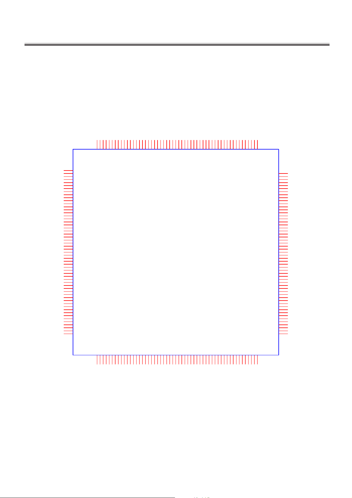
U29 (4MX16BIT BANKS DDR) M13S2561616A-5TG2K
-14-
Page 15
IC Block Diagram
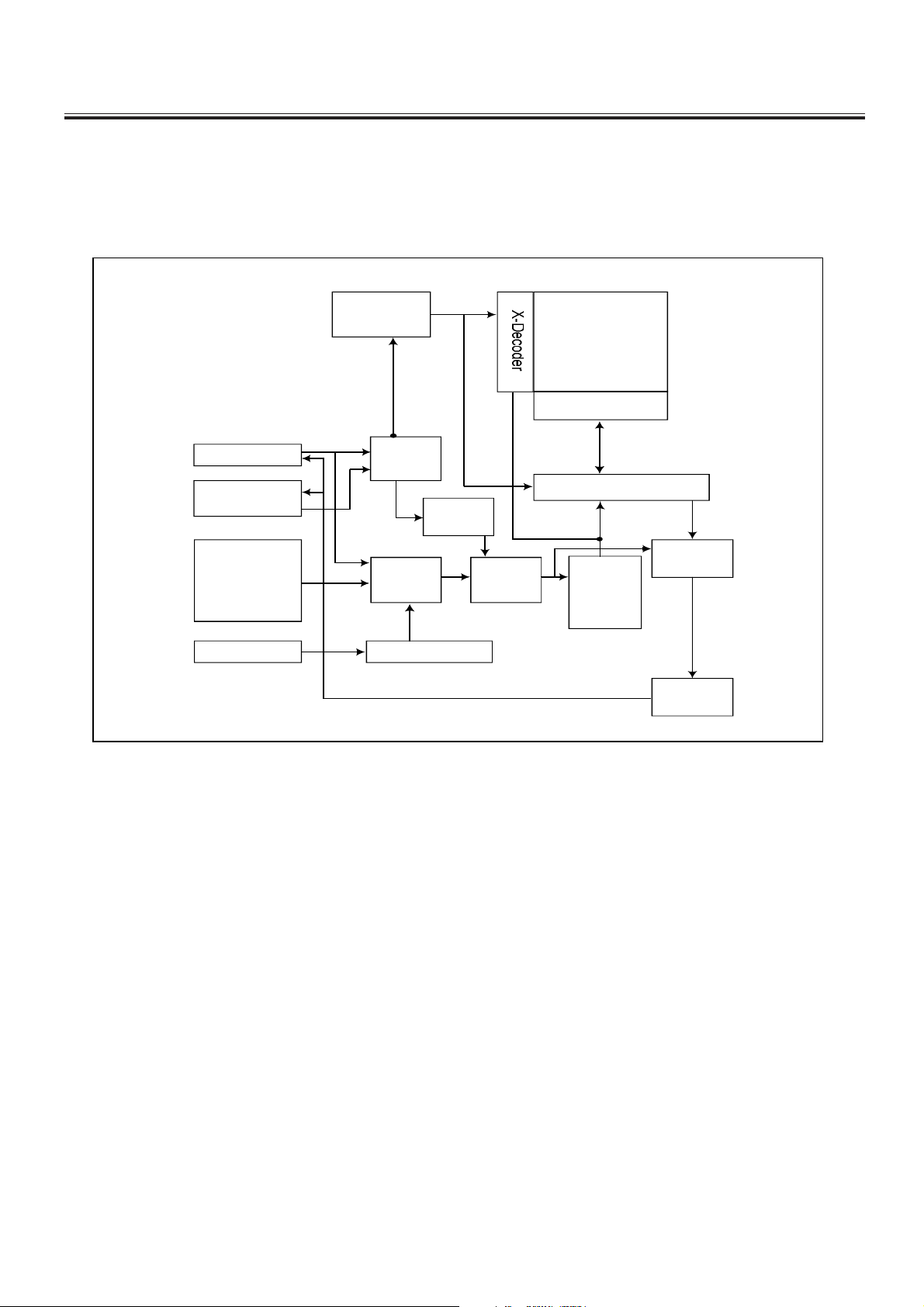
8᧤0%,7&0266(5,$/)/$6+᧥623
Address
Generator
MemoryArray
Page Buffer
SI/SIO0
SO /S IO1
CS#,
WP#,
HOLD#
S CLK Clock G enerator
Data
Register
SRAM
B uffer
M ode
Logic
S tate
Machine
Y-D ecoder
Sense
Am plifier
HV
Generator
Output
B uffer
-15-
Page 16
IC Block Diagram
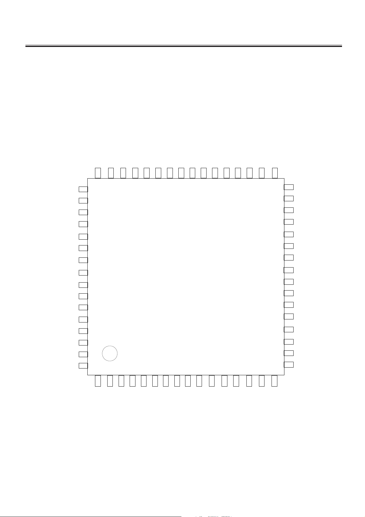
U19(HDMI SWITCH) PS331TQFP64G
SiI9185 Pin Mapping
POW_SINK
HPD3
SDA3
SCL3
B31
A31
POW3
B32
A32
GND
B33
A33
VCC
B34
A34
CEXT
49
50
51
52
53
54
55
56
57
58
59
60
61
62
63
64
SDA_SINK
48 47
Z1
SCL_SINK
46
HPD_SINK
Y1
Y2
Z2
45 44 43 42 41
GND
Z4
Z3
Y3
VCC
Y4
PS331
1
2 3 4 5 6 7 8 9 10 11 12 13 14 15 16
I2C_ADDR
SCL_CTL
SDA_CTL
3334353637383940
POWDN
32
31
30
29
28
27
26
25
24
23
22
21
20
19
18
17
REXT
A14
B14
NC
A13
B13
GND
A12
B12
VCC
A11
B11
SCL1
SDA1
I2C_RST
B21
SDA2
HPD2
SCL2
A21
B22
POW2
A22
GND
B23
A23
B24
VCC
A24
HPD1
POW1
-16-
Page 17
IC Block Diagram
U1(DUAL BTLCLASS DAUDIO AMPLIFIER) TPA3113D2
SD
FAULT
LINP
LINN
GAIN0
GAIN1
AVCC
AGND
GVDD
PLIMIT
RINN
RINP
NC
1
2
3
4
5
6
7
8
9
10
11
12
13
28
27
26
25
24
23
22
21
20
19
18
17
16
PVCCL
PVCCL
BSPL
OUTPL
PGND
OUTNL
BSNL
BSNR
OUTNR
PGND
OUTPR
BSPR
PVCCR
PBTL
14
-17-
15
PVCCR
Page 18

-18-
Page 19

Main PCB Top/Bottom Layer
-19-
Page 20

Main PCB Top/Bottom Layer
-20-
Page 21

8M26S Factory Adjust Menu
(V0.2)
1. Description
Enter factory mode:
Open source menu,and then press digital button “3”, “1”, “9” , “5” in
turns to enter the factory menu. Press ↑ and ↓ button to choose the
item, press OK button enter the submenu, press ← and → button to
adjust the value.
Leave factory mode:
Press menu button to back to upper menu until leave factory mode。
Software information:
Enter factory mode, you can get the software information from the
bottom of menu.
Panel information:
Enter factory mode, enter “PANEL SETTING” item, you can get the
panel information from the bottom of menu.
Aging mode:
Enter factory mode, select “SYSTEM SETTING” item, press OK
button enter, select “AGING MODE” item, press → button open aging
mode.
Note: You can press the shortcut key in the factory remote control to
open or close the aging mode.
-21-
Page 22

ADC adjusts:
YPBPR source ADC:
Switch to YPBPR source, input 100% color bar pattern, enter
factory, select “AUTO ADC” item in the “ADC CALIBRATION”,
press → button to begin auto adjust. When it is finish, it will show
“OK” or “FAILE”. If “FAILE” is showed, you need to try again.
NOTE: YPBPR ADC need to do twice by use 576P and 720P
signal separate.
VGA source ADC:
Switch to PC source, input tessellated white and black signal,
enter factory, select “AUTO ADC” item in the “ADC CALIBRATION”,
press → button to begin auto adjust. When it is finish, it will show “OK”
or “FAILE”. If “FAILE” is showed, you need to try again.
-22-
Page 23

White balance:
Enter factory mode, enter “WHITE BALANCE” item, you can adjust
white balance in this menu.
Over scanning:
Enter factory mode, enter “PANEL SETTING” item, enter
“OVERSCAN” item, you can adjust the over scan in this menu.
Factory reset:
Enter factory mode, enter “SYSTEM SETTING” item, select “FAC
RESET DEFAULT” item and press OK button to reset the flash
memory. TV set will restart when it is finish.
Update software (by USB):
Copy the new software (name by “MERGE.bin”) to the root directory
of USB drive. Plug the drive to the USB socket (if there are two USB
socket, make sure you use the socket 1). Enter factory, select “Software
Update (USB)” item and press OK button to begin update. TV set will
-23-
Page 24

restart when finish. Note, you need to restart the TV set again by AC
power.
We suggest you need to do “Factory reset” after software update.
-24-
Page 25

2. More information
FACTORY MENU Default Value Remark
ADC CALIBRATION
MODE Select source
R-GAIN Red gain
G-GAIN Green gain
B-GAIN Blue gain
R-OFFSET Red offset
G-OFFSET Green offset
B-OFFSET Blue offset
AUTO ADC Auto ADC calibration
WHITE BALANCE
MODE Select source
TEMPERATURE Select Neutral/Warm/Cool/Personal
R-GAIN Red gain
G-GAIN Green gain
B-GAIN Blue gain
R-OFFSET Red offset
G-OFFSET Green offset
B-OFFSET Blue offset
COPY ALL Copy there values to all source!
PANEL SETTING
TI MODE LVDS data format
LVDS PORT LVDS data interface
-25-
Page 26

LVDS BIT
PWMFREQUENCY TTL PWM frequency
PWM DUTY TTL PWM duty
OVERSCAN
OVERSCAN_RESLUTION
HPOSITION Horizontal position
VPOSITION Vertical position
HSIZE Horizontal size
VSIZE Vertical size
SYSTEM SETTING
FAC. HOTKEY Factory hot key enable
TTX BRI Teletext brightness
WHITE PATTERN White test pattern enable
POWER REMIND No signal power off time
BLUE SCREEN No signal blue screen enable. (TV source exclusion)
VIDE AGC Vide AGC
DLC DLC enable
WHITE BLACK STRENTH White/black strength enable
POWER CONDITION Power state remember
FAC RESET DEFAULT Reset all value to factory default
OUT FACTORY SET Reset some value to out box mode
AGING MODE Aging mode enable
NO SIGNAL MUTE AMP Mute ampler No signal
AGC GAIN Vide AGC gain
LANGUAGE SETTING
-26-
Page 27

S-CHINESE
SPANISH
FRENCH
PORTUGUESE
BGI CHINESE
SOURCE SETTING
TV
AV1
AV2
AV3
SCART
HDMI1
HDMI2
HDMI3
YPBPR1
USB1
USB2
ANALOG CURVE
MODE
PICTURE MODE
BRIGHTNESS CURVE
CONTRAST CURVE
SATURATION CURVE
HUE CURVE
SHARPNESS CURVE
-27-
Page 28

VOLUME CURVE
BACKLIGHT
HOTEL FUNCTION
HOTEL MODE Hotel mode enable
IR LOCK
LOCAL KEY LOCK
USER SETTING SAVE
VOLUME FIXED
POWER ON VOL VALUE
MAX VOLUME
POWER ON SOURCE
SCALE LOCK
CHANNEL SEARCH LOCK
OTHER OPTION
SSC LVDS and DDR frequency setting
UART DEBUG Debug port mode
VIF1 VIF setting
POWER ON LOGO Logo enable
NICAM Nicam enable
LOGO SET IN USB Setting logo by use the USB picture
USB SRC NAME Change USB name: UPLAY/USB/MEDIA
Software Update(USB)
-28-
Page 29

EXTERNAL SCHEMATIC AND INSTALLATION
Front Panel
Note: The graphics are for representation only.
2
3
3
CHVOL
MENU
SOURCE
4
5
6
7
8
1
1.Power Button
2.Power Indicator / Remote Sensor
3.Speakers
4.Channel Up/Down Button
5.Volume Up/Down Button
6.Menu Button
7.Source Button
8.Standby Button
-29-
Page 30

EXTERNAL SCHEMATIC AND INSTALLATION
Back Panel
Note: The graphics are for representation only.
MEDIA1 MEDIA2
9
HDMI1 HDMI2
VIDEO VIDEO
Y
2
PC IN
1
S/PDIF
P
b
LEFT
RIGHT
P
r
PC
YPbPr IN
AUDIO IN
AV2 IN
345 6 7
LEFT
RIGHT
AV OUT
75 ANT
8
RIGHT
LEFT
AV1 I N
VIDEO
1.PC IN: Connect a PC via a VGA cable.
2. HDMI1\HDMI2:Connect HDMI input signal from signal source such as DVD.
3. PC AUDIO IN: Audio input for PC and Audio input.
4. S/PDIF: Use a digital optical cable to connect your TV to a compatible audio receiver.
5. Y Pb Pr(Component input): Connect YPbPr signal from signal source such as DVD.
6. AV1 IN / AV2 IN: Connect AUDIO and VIDEO input signal from signal source such as DVD.
7.
AV OUT: Connect AUDIO and VIDEO output signal.
8. RF IN: Connect a coaxial cable to receive signal from the antenna or cable.
9. MEDIA1\MEDIA2: MEDIA port.
10. EARPHONE: Audio output, speakers will be muted when earphone plugged.
6
10
-30-
Page 31

EXTERNAL SCHEMATIC AND INSTALLATION
Antenna /Cable Connection
There are two kinds of antenna in use.
VHF TV ANTENNA
UHF TV ANTENNA
U/V MIXER
TWO KINDS OF ANTENNA
COAXIAL ANTENNA
FLAT CABLE
No need to install adapter
(Note 1)
Need to install adapter
(Note 2)
To TV VHF/UHF
ANTENNA jack
VHF/UHF
(75 )
1. Connect the plug of the antenna cable or CATV cable to the cable (not provided
with this unit), then connect to the antenna input of this unit for best reception.
2. If the antenna cable in your home is other than the above two, or you have
problems in installing the antenna, please contact your dealer.
Notes:
1. Current outdoor antenna or cable TV usually use 75 OHM coaxial antenna cable.
For better using this kind of antenna cable.reception, we suggest
2. Flat cable or indoor antenna are old designed, the reception may not be good enough.
-31-
Page 32

EXTERNAL SCHEMATIC AND INSTALLATION
Remote Control
1. Standby( )
Press to turn the TV on or off(standby).
2. Picture Mode( P.P )
Press to select the desired picture
mode.
3. Sound Mode( S.M )
Press to select the desired sound mode.
4.ZOOM
Press to select the desired picture aspect ratio.
5. SLEEP
Press to set the time to switch the TV to
standby mode.
6. Program Select (0-9)
Press to select the TV channel directly.
7.RECALL
Press to return to previously viewed channel.
8. FREEZE
Press to freeze or unfreeze the picture.
9.Mute( )
Press to mute or restore the volume.
10.Channel Up/Down
(CH / )
Press to select previous/next channel.
11.Volume Up/Down (V+/V-)
Press to adjust the volume.
12.MTS (Option)
Press to select a different sound mode when
the source is different.
13.Menu
Press to enter or exit from the TV menu.
14.Source
Press to select the input source mode.
10
12
13
1
2
3
6
7
9
5
4
8
11
14
-32-
Page 33

EXTERNAL SCHEMATIC AND INSTALLATION
Remote Control
15.OK
Press to confirm and execute the selection.
16. Up/Down/Left/Right Cursor
( / / / )
Press to select or adjust the desired item
on the menu.
17.CC button
Press to select the CCD or OFF.
18.INFO
Press to display relevant information such as
screen format, source, etc.
19.MEDIA
Press to the MEDIA menu.enter
20.Fast Backward Button( )
Press to fast reverse in Media mode.
21.Fast Forward ( )
15
17
19
20
24
22
16
18
21
25
23
Press to fast forward in Media mode.
22.Previous ( )
Press to play the previous
Media
mode.
music or movie in
23.Next ( )
Press to play the next
Media .
mode
music or movie in
24.Play & Pause ( )
Press to pause playback in Media mode,
press again to continue playback.
25.Stop ( )
Press to
Media
stop the music or movie in
mode.
-33-
Page 34

MENU CONTROL
This section explains the menus of your TV. Each menu is outlined and detailed to help you
get the most from your TV.
Basic Operation
1. Press MENU on the remote control or on the TV key
panel to display the main menu.
2. Press / and / to highlight the desired menu/item.
3. Press / to change the setting.
4. Press MENU to save setting and go back to last menu.
Note:
Button on the key panel have the same functions
as the corresponding buttons on the remote control.
The scheme and description are in TV mode as below, there will be a note if there is exception.
Picture Settings
Picture Mode
Adjusts the picture mode: Personal, Bright, Normal,
Soft four kinds of image mode.
Brightness
Adjusts the brightness of the picture, and usually is
adjusted together with Contrast.
Contrast
Adjusts the difference between the light and dark areas
of the picture. To get better picture value, Contrast should
be adjusted to the proper value.
Color
Adjusts the richness of color. This function is not available
in PC mode.
Tint
A
djust the tint of the picture.
Only can be done under the NTSC system.
Sharpness
Adjusts the sharpness of the picture. This function is not
available in PC mode.
Color Temperature
Press OK button to enter the color temperature sub menu.
Color Temperature Adjusts the colour temperature of the
picture, to select the option:
Cool, Neutral, Warm, Personal
as you desired.
PICTURE
Picture Mode
Brightness
Contrast
Color
Tint
Sharpness
Color temperature
PICTURE
Display Mode
DNR
PICTURE
Color Temperature
Red
Green
Blue
Personal
LOW
Soft
16:9
55
50
20
50
50
50
50
50
-34-
Page 35

MENU CONTROL
Neutral: Keep the original white
Warm: Red
Personal
Cold: Blue.
Display Mode
To select different display mode.
DNR
To select four modes of digital noise reduction are available including Off, Low, Middle and High.
Sound Settings
Sound Mode
Select the most suitable sound mode according to
your watching contents(
Film, News).
Bass
Control the level of low-pitched sound.
Treble
Control the level of high-pitched sound.
Balance
Control the audio balance between the right and left
TV speakers.
AVL
This function may be set as On or Off. Auto Volume Level
can set the volume automatically adjust corresponding to
the input audio.
Surround
Press this option to enter to set On or Off.
Equalizer
Adjust the frequency bands of sound to suit the type of sound broadcast.
: The user may customize the color temperature.(Red/Green/Blue).
SOUND
Personal, Standard, Music,
Sound Mode
Bass
Treble
Balance
AVL
Surround
Equalizer
EQUALIZER
120Hz
500Hz
1.2KHz
7.5KHZ
12KHz
Personal
Off
Off
50
50
0
50
50
50
50
50
-35-
Page 36

MENU CONTROL
Installation Settings
Note: These settings are only available in TV mode.
Channel No.
Sets the received TV channel No.
Colour system
Selects colour system.
Auto Search
Searches and saves channels automatically.
Fine Tuning
Effect on the current TV signal images
are not satisfied, you can use this function to adjust.
Channel Skip
You can skip unnecessary program channels of your
choice not to be displayed during viewing and scanning
when pressing the buttons. Select "OFF" by
" " b
pressing uttons to select the channel that would
" "
CH /
not like to skip from the channel scan operation.
Signal Source
" " Press button to adjust the Signal Source
which can choose "Air, Cable".
Setup Settings
OSD Language
Select you desired OSD language.
Lock Panel Keys
Set On/Off to Lock or unlock the control on the panel.
CCD
Select the type of CCD.
User Reset
Restore the menu setting back to default.
INSTALLATION
Channel No.
Color System
Auto Search
Fine Tuning
Channel Skip
Signal Source
TV : 0 Channel
CH 11 56.00 Mhz (Air)
SETUP
OSD Language
Lock Panel Keys
CCD
User Reset
Auto Search
MENU
1
NTSC
53.00MHz
Off
Air
English
Off
Off
-36-
Page 37

MENU CONTROL
Advanced Settings
Press / button to select Advanced menu, then press [OK]
button to enter. Input password to enter, default password is
0000 .
""
Enter password
Clear Cancel
Free Record Limit 6Hr.
Change Password
To set your own password, first enter the old password, and then enter your new password twice,
following the prompts as illustrated below.
Enter OldPasssword
Enter newPassword
Confirm Password
Clear Cancel
Free Record Limit 6Hr.
Note:
- Default password is [0000].
- In the event whereby new password is forgotten, it can be reset to default password. Please be mindful
that all other picture and audio settings will also be reset to default values.
ADVANCED
Set Password
V-CHIP
TV-Rating
Movie-Rating
English-Rating
French-Rating
Block No Rating
Off
PG
C8+
G
No
V-CHIP
set V-CHIP on or off.Press to
/
TV-Rating
Press to enter the TV Rating menu.
Press [OK] button to set rating block or unblock.
Movie-Rating
Press to select the Movie Rating
/
TV-Y
TV-Y7
TV-G
TV-PG
TV-14
TV-MA
(None / G / PG / PG-13 / R / NC-17 / X).
English-Rating
Press to select the English Rating
/
(Empty / C / C8+ / G / PG /14+ / 18+).
French-Rating
Press to select the French Rating
/
(Empty / G / 8ans+ / 13ans+ / 16ans+ / 18ans+).
Block No Rating
Press to set the function Block or Unblock the not rating singal.
/
-37-
ALL
ALL
ALL
ALL
ALL
ALL
TV RATING
FV
V
V
V
S L D
S L D
S L
Page 38

MENU CONTROL
PC Settings
Note: These settings are only available in PC mode.
when you connect VGA cable to the jacks of PC and
select the signal source as "PC" the screen menu will
be activated. You can use the function to adjust the
display setting automatically or manual.
AUTO ADJUST
Press
" " button to auto adjust PC size and position.
H Position
" " button to adjust the H-Position of the
Press
television.
V Position
" " button to adjust the V-Position of the
Press
television.
Phase
Press
" " button to adjust the phase of the picture.
Frequency
" " button to adjust the updating frequency
Press
of the picture.
Auto Adjust
H Position
V Position
Phase
Frequency
PC
50
50
50
50
-38-
Page 39

MEDIA CONTROL
Gentle Reminder When Using The Media Player
1.Some USB storage devices may not be compatible to operate smoothly with this TV.
2.Back up all of the data in the USB storage device in case if data was lost due to unexpected
accident. We do not assume any liability for the losses by misuse or malfunction. Data backup
is consumer's responsibility.
3.For large file sizes, the loading speed may be slightly longer.
4.The recognition speed of a USB storage device may depend on each device.
5.When connecting or disconnecting the USB storage device, ensure that the TV is not in Media
mode otherwise the USB storage device or the files stored in it may be damaged.
6.Please use only a USB storage device which is formatted in FAT16, FAT32, NTFS file system
provided with the Windows operating system. In case of a storage device formatted as a
different utility programme which is not supported by Windows, it may not be recognized.
7.When using a USB Hard Disk Drive which requires electric power source, ensure its power
does not exceed 500mA.
8.An "Unsupported File" message will be displayed if the file format is unsupported or corrupted.
Caution
Use cable with the following maximum thickness for optimal connection to this TV,
or it may damage your TV.
1.HDMI Cable not exceeding 10(A) x 20(B)mm
2.MEDIA Cable not exceed by 7(A) x 18(B)mm
* Dimension of (A) should not be exceed 10mm.
In situation whereby the insertion of USB storage
device is restricted, user may use the USB
extension accessory provided.
Media File Playback Support
Supported Video File :
File Extension
dat, mpg, mpeg
ts, trp
Container Video Codec SPEC
MPG, MPEG
MPEG2 -TS MPEG2
Supported Music File:
Audio Codec
MPEG1 Layer2
MPEG1 Layer3
File Extension Bit Rate
MP3(Option) 32Kbps ~ 448Kbps(Bit rate) 32KHz ~ 48KHz(Sampling rate)
MP3(Option)
Supported Photo File:
Image
JPEG
PNG
BMP
Supported Text Format : (*.txt)
Photo Resolution
Base-line 15360x8640
Progressive
Non-interlace 9600x6400
Interlace 1200x800
Encoding standard : Unicode
Mpeg1,2
32Kbps ~ 320Kbps(Bit rate) 32KHz ~ 48KHz(Sampling rate)
1024x768
9600x6400
720P @ 30P
720P @ 30P
Bit Rate
20Mbit/sec
20Mbit/sec
Profile
Main Profile
MPEG2: Main Profile
1
-39-
Page 40

MEDIA CONTROL
Remote Control
1.MEDIA buttons
Press to enter MEDIA menu.
2.Fast Backward buttons( )
Fast reverse while playback.
3.Fast Forward buttons( )
Fast forward while playback.
4.Previous buttons( )
Press to return to the previous chapter
/track/photo. Skip to previous file.
5.Next buttons( )
Press to skip to the next chapter/track/photo.
Skip to next file.
6.Play & Pause buttons( )
Press to pause play and
press again to make play continue.
7.Stop buttons( )
Press the stop button to exit full-screen
playback, access to the preview.
MEDIA Menu
You can play video and music , view photo and text files from you USB storage devices.
1.Connect USB storage device to MEDIA input terminal.
2.Press MEDIA button to enter MEDIA mode.
3.Press [ ] / [ ] and ]to select the types of media modes: VIDEO, MUSIC, PHOTO
and TEXT.
Device 2.0
music or movie
VIDEO
MUSIC
-40-
PHOTO
TEXT
Page 41

MEDIA CONTROL
Video Menu
1.Press [ ] / [ ] to select VIDEO. Press
[ OK ] to enter.
2.Press [ ] / [ ] to select the desired drive
and press [ OK ] to enter.
3.Press [ ] / [ ] to select the desired folder
and press [ OK ] to open the folder; select the
desired video file using [ OK ] and press [ ]
to start playing.
4.Press [ ] to stop video playing and return
to video list.
5.You may return to Media Player main menu
by pressing [ MEDIA ].
Video Control Bar
Pause
Fast Reverse
Fast Forward Previous
Return
VIDEO
3inl.rmvb
C: \
MEDIA
Exit Mark Select
OK
Next
1/1
StopAPlay Mode
Resolution: 720 X 480
Audio Track: 1/1
Subtitle: --/0
Program: --/0
Size: 967 KBytes
AB
Repeat Play
Display Mode
LIST
Current Information
Move
I
Election Play
Zoom In
Zoom Out
- Press [ INFO ] to display Video Control Bar while playing the video.
- Press [ ] / [ ] to select the desired settings.
- Press [ ] to exit from Info bar.
There are three modes of play mode. Press [OK] button to select Current Track( ), Repeat
None( ) and All Tracks( ).
1
A
1
-41-
Page 42

MEDIA CONTROL
Music Menu
1.Press [ ] / [ ] to select MUSIC. Press
[ OK ] to enter.
2.Press [ ] / [ ] to select the desired drive
and press [ OK ] to enter.
3.Press [ ] / [ ] to select the desired folder
and press [ OK ] to open the folder; select the
desired music file using [ OK ] and press [ ]
to start playing.
4.Press [ ] to stop music and return to
Music list.
.You may return to Media Player main menu
5
by pressing [ MEDIA ].
Music Control Bar
Pause Fast Reverse Fast Forward
I
Previous Next
Return
MUSIC
Super Star.mp3
C: \
MEDIA
OK
Exit Mark Select
1/1
Stop
Album: Http://www.ccyy.com
Title: SuperStar Size:
Bit Rate : 128K 967 KBytes
Artlist :5mm
Sampling :44K
Year: 2008
Play Mode
A
Mute
List
Current Information
Election Play
- Press [ INFO ] to display Music Control Bar while playing the music.
- Press [ ] / [ ] to select the desired settings.
- Press [ ] to exit from Info bar.
Note:
-
This menu only shows support files.
- Files with other file extensions are not displayed, even if they are saved on the same USB storage device.
- An over-modulated mp3 file may cause some sound distortion during playback.
- This TV supports lyrics display (English).Maximum number of characters per line is 48.
- The filename of music and lyrics must be the same in order to display lyrics while the music is playing.
-42-
Page 43

MEDIA CONTROL
Photo Menu
1.Press [ ] / [ ] to select PHOTO. Press
[ OK ] to enter.
2.Press [ ] / [ ] to select the desired drive
and press [ OK ] to enter.
3.Press [ ] / [ ] to select the desired folder
and press [ OK ] to open the folder; select the
desired photo file using [ OK ] and press [ ]
to start playing.
4.Press [ ] to stop photo slide show and
return to Photo list.
.You may return to Media Player main menu
5
by pressing [ MEDIA ].
Photo Control Bar
Pause
Previous Next
Stop
Return
PHOTO
Picture01.jpeg
C: \
MEDIA
OK
Exit Mark Select
Play Mode
1/1
Music
A
Resolution: 1024 X 768
Size: 983 KBytes
Date: ----/--/-Time: --:--:--
List
I
Current
Information
90
Clockwise
90 Degrees
90
Counterclockwise
90 Degrees
Zoom In
Zoom Out
- Press [ INFO ] to display Photo Control Bar during photo slide show.
- Press [ ] / [ ] to select the desired settings.
- Press [ ] to exit from Info bar.
-43-
Move
Page 44

MEDIA CONTROL
Text Menu
1.Press [ ] / [ ] to select TEXT. Press [ OK ]
to enter.
2.Press [ ] / [ ] to select the desired drive
and press [ OK ] to enter.
3.Press [ ] / [ ] to select the desired folder
and press [ OK ] to open the folder; select the
desired text file using [ OK ] and press [ ]
to display the text document.
4. Press [ ] / [ ] to view previous or next
text file.
5. Press [ ] / [ ] to select previous or next
page in the text file.
6. Press [ ] to return to Text list.
.You may return to Media Player main menu
7
by pressing [ MEDIA ].
Text Control Bar
Fast Reverse
Fast Forward Previous Next
- Press [ INFO ] to display Text Control Bar while reading the text.
- Press [ ] / [ ] to select the desired settings.
- Press [ ] to exit from Info bar.
Note:
- It supports *.txt files.(English character)
- Please ensure that the text file is saved in an encoding standard. This may minimize the loss of characters
in a multiple-language content.
Stop
Return
TEXT
Text01.txt
C: \ 1/1
MEDIA
OK
Exit Mark Select
List
Music
Current Information
Please ensure that the text
file is saved in an encoding
standard (eg.Unicode).
This may minimize the loss
of characters ina multiplelanguage content.
Size: 20 KBytes
I
-44-
Page 45

TROUBLESHOOTING
NO PICTURE, NO SOUND
1. Check if the fuse or circuit breaker is working.
2. Plug another electrical device into the outlet to
make sure it is working or turned on.
3. Power plug is bad contact with the outlet.
4. Check the signal source.
NO COLOR
1. Change the color system.
2. Adjust the saturation.
3. Try another channel. Black-white program may
be received.
REMOTE CONTROL DOES NOT WORK
1. Change the batteries.
2. Batteries are not installed correctly.
3. Main power is not connected.
NO PICTURE, NORMAL SOUND
1. Adjust the brightness and contrast.
2. Broadcasting failure may happen.
NORMAL PICTURE, NO SOUND
1. Press the volume up button to increase volume.
2. Volume is set to mute, press MUTE to restore
sound.
3. Change the sound system.
4. Broadcasting failure may happen.
SNOWY DOTS AND INTERFERENCE
If the antenna is located in the fringe area of a
television signal where the signal is weak, the
picture may be marred by dots. When the signal
is extremely weak, it may be necessary to install
a special antenna to improve the reception.
1. Adjust the position and orientation of the
indoor/outdoor antenna.
2. Check the connection of antenna.
3. Fine tune the channel.
4. Try another channel. Broadcasting failure may
happen.
IGNITION
Black spots or horizontal streaks appear, or the
picture flutters or drifts. This is usually caused by
interference from car ignition system, neon lamps,
electric drills, or other electrical appliance.
GHOST
Ghosts are caused by the television signal
following two paths. One is the direct path, the
other is reflected from tall buildings, hills, or other
objects. Changing the direction or position of the
antenna may improve the reception.
RADIO FREQUENCY INTERFERENCE
This interference produces moving ripples or
diagonal streaks, and in some case, loss of
contrast in the picture. Find out and remove the
radio interference source.
UNORDERLY RIPPLES ON THE PICTURE
It is usually caused by local interference, such as
cars, daylight lamps and hair driers. Adjust the
antenna to minimize the interference.
BLANK SCREEN IN PC MODE
Perhaps the TV can not recognize the resolution set
by the PC. Suggest to change to the best resolution
or other standard resolutions of Windows system.
Set refresh rate to be 60Hz.
-45-
Page 46

g
,
g
p
pp
y
b
p
pp
y
b
Q
pp
y
pp
y
b
Service Flow Chart
Done
Main
oard
Done
Change the
Done Done
Change the
fuse on power
supply board
N
Y
AC line
Check the
“ATMEL 24C64”
the fuse
Change
power supply
Change the
oard
Chang the power
su
l
IC for U9
N
Main IC “U9”
N
Change the
N
Y
Done
N
Y
Check all DC power
su
l
on U41
Done
N
Check the AC input on
ower su
l
board
Y
Change the EEPROM U43
N
Upgrade the software
N
Check the 5VSTB on “CON8”
N
Y
No audio & No backli
Led indicator “red” on
Done
Done
Upgrade the
software
Done
Change the “U41” Done
Done
N
Y
N
Y
“
Change the
3” or “U9”
Upgrade the
software
Y
Done
ht
Upgrade the
N
Check the 5V, 12V & 24V
N
Y
Press the “ON/OFF” on keyboard &
remote control
led turns
reen
Y
Done
oard
on “CON8”, should
power supply
Change the
“ON/OFF” voltage
Check the
N
Done
“U41” Pin81 if
it works well.
Y
Check “Q3” &
N
be greater than 2.7V
software
Y
N
on
ower su
l
board
Y
Done
the panel.
Change
Y
Y
-46-
Page 47

p
p
Service Flow Chart
Fix the mute circuit Upgrade the software
Done
Change the mainboard
N
Done
OK
Done
Change the main
IC “U41”
Done
N
OK
N
Check the mute circuit
if it is OK.
=0V
Check the voltage of “Mute” pin beside
the am
Y
>0V
lifier IC. It should not be 0V.
Check the audio input line
& the audio in
N
N
Done
OK
ut circuit.
Done
Check if the Volume has set to “0”
or if the it is mute
Has video but no audio
Y
-47-
Page 48

r
y
gg
pp
y
Service Flow Chart
Well connect the cable Check the current input
Done
OK
Change the mainboard
N
Done
Change the tuner
Done
OK
Done
Change the
mainboard
N
Change the Q29 & U25
N
Check the Q29 & U25 circuit
Done
N
Fix the DC supply
OK
mainboard
N
su
l
of the tuner.
Change the
N
Done
OK
Check the DC power
N
Change the main
IC “U41”
N
source if it is TV
follow the workin
Y
Adjust AGC
N
it has exactl
connected
Y
Check the cable input if
N
Check the Color / Saturation
in picture menu if it has
decreased to “0”
N
Has video but no colo
N
Done
OK
Done
OK
Done
N
OK
Check the Q29 & U25 circuit
Y
to default “50”
OK
Done
uide.
Done
OK
Y
Increase the item
-48-
Page 49

b
g
r
Q
(
,
)
p
r
b
Service Flow Chart
inverter line is 24V
Check the voltage of
Done
Done
Upgrade the
software
Done
Change the “U9”
N
“
3” or “U41”
N
software
Change the
Upgrade the
Y
Done
N
it works well.
OK
N
Done
“U41” Pin81 if
Check “Q3” &
N
N
OK
be greater than 2.7V
on “CON8”, should
Safely connect the
inverter line
“ON/OFF” voltage
Check the
N
ackli
ht inve
ter connected
Y
Check the connector of
N
Check if the backlight is on
Has audio but no video
Done
Done
main
oard
the panel.
YY
Change the
Done
N
OK
main IC U41
Done
Chane the
Change
owe
OK
“ATMEL 24C64”
N
Y
Done
Correct the
N
Change the EEPROM U43
OK
N
Safely connect the
LVDS line
N
Make sure the LVDS power is correct
5V for 26”
12V for 32”&42”
Y
N
Check the LVDS line
if it is connected
Y
Done
Done
OK
-49-
Y
Page 50

1
2
+1.2V_VDDC
U50-3
3
U50
E3482
U50
E3482
2
600mA
C162
C162
C163
C163
L47L47
R62 100_1%R62 100_1%
C18
10nF
C18
10nF
OUT
EN
VCC
COMP
7
6
0.1u
0.1u
10uF
10uF
+
+
R57 1.91K_1%R57 1.91K_1%
U50-5
1
BST
SS
8
CA18
CA18
470uF/16V
470uF/16V
C17
C17
R55
4.7K_1%
R55
4.7K_1%
0.1uF
0.1uF
+5V
5
FB
GND
Vout=0.923*(1.91K+4.7K)/4.7K=1.3V
U49
E3482
U49
4
E3482
L40
L40
BEAD/22uH/DIP
BEAD/22uH/DIP
C15
C15
3
OUT
VCC
2
7
R46
R46
EN
C175
C175
22K_1%
22K_1%
10nF
10nF
COMP
6
SYSTEM_POWER V1.0
MST6M181VS
SYSTEM_POWER V1.0
MST6M181VS
SYSTEM_POWER V1.0
MST6M181VS
A3
A3
A3
Size Document Number Rev
Size Document Number Rev
Size Document Number Rev
H7NCH7
NC
1
NC
of
110Friday, August 03, 2012
110Friday, August 03, 2012
110Friday, August 03, 2012
1
Date: Sheet of
Date: Sheet of
Date: Sheet
2
+
+
CA15
100uF/16V
CA15
100uF/16V
+2.5V_Normal
300mA
U27
0.1u
0.1u
+
+
CA16
CA16
470uF/16V
470uF/16V
R48
R48
4.7K_1%
4.7K_1%
U27
4
OUT
OUT
ADJ
ADJ
H20NCH20
IN
IN
NC
AMS1117-25
AMS1117-25
3
2
1
R56
R56
1
100mA
U20
1
BST
5
FB
C13
C13
0.1uF
0.1uF
GND
Vout=0.923*(22K+4.7K)/4.7K=5.2V
4
SS
8
U20
4
OUT
OUT
ADJ
ADJ
IN
IN
AMS1117-3.3
AMS1117-3.3
3
2
1
NC/180_1%
NC/180_1%
+5V_Normal
C381
C381
C386
C386
+3.3V_Standby
C47
C47
C385
C385
C51
C51
C66
0.1u
C66
0.1u
C390
2.2u
C390
2.2u
Vout=1.25*(1+180/180)=2.5V
Vout=1.25*(1+R60/R56)
C67
0.1u
C67
0.1u
R60
R60
0R/180_1%
0R/180_1%
nearest to MST6M181 PIN
10uF
10uF
2.2u
2.2u
0.1u
0.1u
U23
2.2u
2.2u
0.1u
0.1u
U23
4
OUT
OUT
ADJ
ADJ
IN
IN
SHIELD SHIELD-6SHIELD SHIELD-6
+3.3V_Normal
AMS1117-3.3
AMS1117-3.3
3
2
1
50mA
C391
2.2u
C391
2.2u
C54
0.1u
C54
0.1u
C388
2.2u
C388
2.2u
C59
0.1u
C59
0.1u
GND
GND
GND
GND
GND
GND
6
5
4
3
2
1
<OrgName>
Title
<OrgName>
Title
<OrgName>
Title
H8NCH8
H9NCH9
NC
NC
1
1
6
7
8
9
1
H2NCH2
5
2
3
4
+5V_Normal
3
U6
AS5406U6AS5406
4
+5V_Standby
5
BL-ADJUST
BL-ON/OFF
12345678910111213
CN10
CN10
3
BS
IN
4
+5V_Normal U50-3
R23
R23
R52 100KR52 100K
4.7K
4.7K
C14
3.3nF
C14
3.3nF
C121
0.1uF
C121
0.1uF
+
+
CA51
CA51
100uF/16V
100uF/16V
EN
1
R54 NC/1KR54 NC/1K
C28
C28
PWR-ON/OFF
R340 200RR340 200R
C27
C27
STANDBY
+12V_ONLY
+5V_Normal
R30
R30
U50-5
NC/4.7uF
NC/4.7uF
NC/10nF
NC/10nF
STANDBY
5
2
D D
FB
GND
2.2K
2.2K
+1.2V_VDDC
C29 NC/22pFC29 NC/22pF
+5V_Standby+5V_Standby+5V_Standby+5V_Standby
+12V_NORMAL
+5V_Standby
14
CON10-2.0mm
CON2.0_14
CON10-2.0mm
CON2.0_14
+
+
CA106
100uF16V
CA106
100uF16V
+
+
CA105
CA105
+12V_ONLY+12V_ONLY+12V_ONLY
NC/470uF/16V
NC/470uF/16V
R42 100KR42 100K
R22 NC/0R22 NC/0
C12
C12
C114
C114
+
+
CA48
CA48
P10P10
3.3nF
3.3nF
0.1uF
0.1uF
R25
R25
100uF/16V
100uF/16V
+12V_NORMAL
Q51
NC/M2345
Q51
NC/M2345
R14
R14
+12V_ONLY+12V_ONLY+12V_ONLY+12V_ONLY+12V_ONLY+12V_ONLY+12V_ONLY+12V_ONLY+12V_ONLY+12V_ONLY
3
2.2K
2.2K
C11
C11
+
+
CA104
CA104
NC/0.1u
NC/0.1u
NC/100K
NC/100K
NC/470uF/16V
NC/470uF/16V
2
1
C C
R15
R15
NC/10K
NC/10K
R47
R47
+3.3V_Standby
R411KR41
+5V_Normal
R43
R43
Q4
NC/3904Q4NC/3904
2 3
1
R21 NC/4.7KR21 NC/4.7K
STANDBYSTANDBY
PM GPIO
10K
10K
1K
200R
200R
BL-ON/OFF
BL-ON/OFFBL-ON/OFFBL-ON/OFFBL-ON/OFFBL-ON/OFF
VBL_CTRL
VBL_CTRL
R404.7K R404.7K
1
2 3
Q26
Q26
3904
3904
Q27
Q27
R451K R451K
BL-ADJUST
R49 NC/0R49 NC/0
BRI_ADJ-PWM0
BRI_ADJ-PWM0
20110108 BY LINC46
R354.7K R354.7K
C49 NC/1nFC49 NC/1nF
1
2 3
3904
3904
R44
R44
NC/10K
NC/10K
C46
NC/2.2uF
C46
NC/2.2uF
ᇕ㺙乘⬭ϔ⚍DŽ
C53
1nF
C53
1nF
R58
R58
NC/10K
NC/10K
By lin.20110426
+5V_Normal+5V
Q53
NC/M2345
Q53
NC/M2345
R50 0R50 0
C19
C19
R20
R20
+5V_Standby
NC/0.1u
NC/0.1u
NC/100K
NC/100K
VCC-Panel
Q47
M2345
Q47
M2345
C2
R2
C1
R4 0R4 0
+5V
By lin. 20110421
+12V_NORMAL
R27
NC/100K
R27
NC/100K
Q6
B B
CA119
100uF16V
CA119
100uF16V
+
+
0.1uFC20.1uF
0.1uFC10.1uF
R5 NC/0R5 NC/0
NC/3904Q6NC/3904
2 3
1
R24 NC/4.7KR24 NC/4.7K
STANDBYSTANDBY
PANEL_ON
R3 150KR3 150K
100KR2100K
R51 NC/0R51 NC/0
+5V_Normal
Q1
1
R17 4.7KR17 4.7K
R111
R111
PANEL_ON/OFF
PANEL_ON/OFF
+5V +5V_Standby
3904Q13904
2 3
C6
10K
10K
⫼ϟᢝ⬉䰏ˈֱ䆕ᯊᑣ
IO
0.1uFC60.1uF
6
7
8
9
1
H1NCH1
5
9
NC
2
3
4
6
7
8
1
H4NCH4
5
9
2
3
4
NC
6
7
8
1
H3NCH3
5
40V
D31 1N4148D31 1N4148
L115 220uHL115 220uH
WARNING !!!
R61 10RR61 10R
+12V_NORMAL
A A
3
4
2.2uF/50V
2.2uF/50V
+
+
CA25
CA25
Q44
2SC1815
Q44
2SC1815
R67 4.7KR67 4.7K
Tuner+40V_PWM2
2
NC
3
4
5
Page 51

GAIN1GAIN1GAIN0
ᇍ
ˈ䳔㽕ࡴ
ʽ
+12V_AMP
R533
NC/10K
R533
NC/10K
R532
NC/10K
R532
1
202632
36
1
0
00
0111
GAIN0 GAIN1 AMP
CA107
220uF/16V
CA107
220uF/16V
+
+
C460
0.1uF
C460
0.1uF
2
C459
1nF
C459
1nF
28
PVCCL
SD
U1
U1
1
+12V_AMP
R527
NC/10
R527
NC/10
3
L121 0L121 0
AMP_M
+12V_NORMAL +12V_AMP
NC/10K
C489NCC489
NC
C490NCC490
LP_OUTLP_OUTLP_OUT
LP_OUT
C476
NC/1uF 50V
C476
NC/1uF 50V
BEAD/22uH/DIP
BEAD/22uH/DIP
C486 NC/330pFC486 NC/330pF
L166
L166
R548
NC/10
R548
NC/10
C473
C473
NC/0.22uF 50V
NC/0.22uF 50V
25
27
26
BSPL
OUTPL
PVCCL
LINN
FAULT
LINP
4
2
3
C463 NC/1uFC463 NC/1uF
R543
NC/0
R543
NC/0
GAIN0
C461 NC/1uFC461 NC/1uF
Add by Lin.20110308
AMP_L
NC
LN_OUTLN_OUTLN_OUTLN_OUTLN_OUTLN_OUT
LN_OUTLN_OUTLN_OUT
C477
NC/1uF 50V
C477
NC/1uF 50V
BEAD/22uH/DIP
BEAD/22uH/DIP
C485 NC/330pFC485 NC/330pF
L167
L167
R547
R547
NC/0.22uF 50V
NC/0.22uF 50V
24
22
23
BSNL
PGND
OUTNL
AVCC
GAIN0
GAIN1
7
5
6
C465 NC/1uFC465 NC/1uF
GAIN1
C466
NC/1uF
C466
NC/1uF
R544
NC/0
R544
NC/0
Add by Lin.20110308
R534
10K
R534
10K
R535
10K
R535
10K
RN_OUTRN_OUTRN_OUT
RN_OUTRN_OUT
C474
NC/1uF 50V
C474
NC/1uF 50V
BEAD/22uH/DIP
BEAD/22uH/DIP
NC/10
NC/10
C472
C472
C471
C471
20
21
BSNR
OUTNR
GVDD9RINN
AGND
8
C468
NC/1uF
C468
NC/1uF
R530
R530
C487NCC487
NC
C488NCC488
NC
C484 NC/330pFC484 NC/330pF
L168
L168
R546
NC/10
R546
NC/10
NC/0.22uF 50V
NC/0.22uF 50V
19
18
PGND
OUTPR
PLMIT10RINP
11
C464 NC/1uFC464 NC/1uF
R529 NC/10KR529 NC/10K
ℸ໘ᇣֵোഄ
NC/3.9K
NC/3.9K
RP_OUTRP_OUTRP_OUTRP_OUTRP_OUTRP_OUT
RP_OUTRP_OUTRP_OUT
C475
NC/1uF 50V
C475
NC/1uF 50V
BEAD/22uH/DIP
BEAD/22uH/DIP
C483 NC/330pFC483 NC/330pF
L169
L169
R545
NC/10
R545
NC/10
+12V_AMP+12V_AMP+12V_AMP+12V_AMP
+12V_AMP+12V_AMP
C467
C467
NC/0.22uF 50V
NC/0.22uF 50V
15
16
17
BSPR
PVCCR
PVCCR
NC
PBTL
13
12
14
C462 NC/1uFC462 NC/1uF
AMP_R
+
+
CN2
CN2
CA108
220uF/16V
CA108
220uF/16V
C470
0.1uF
C470
0.1uF
C469
1nF
C469
1nF
TPA3113D2
TPA3113D2
L-OUT
112
2
LP_OUT
LN_OUT
CON2.0_2
CON2.0_2
R536
0/NC
R536
0/NC
U12
U12
R-OUT
CN1
CN1
112
CON2.54_2
CON2.54_2
2
R537
0/NC
R537
0/NC
RP_OUT
RN_OUT
LP_OUT
RP_OUT
470uF/16V
470uF/16V
+
+
+
+
CA13
CA13
CA14 470uF/16V
CA14 470uF/16V
R131
NC/2.2K
R131
NC/2.2K
R128
6
INV2
9
C481 1uFC481 1uF
AMP_R
OUT2
R128
NC/2.2K
NC/2.2K
VP7M/SS
8
AMP_M
+12V_AMP
+5V_Normal
SVRR
3
4
OUT1
GND
17
GND
18
GND
19
GND
20
INV1
1
C480 1uFC480 1uF
AMP_L
GND
GND
GND
GND
GND
GND
GND
GND
GND
+
+
+
+
CA109
CA109
470uF/16V
470uF/16V
5
2
16
15
14
13
12
11
10
TDA1517P
TDA1517P
CA112
100uF/16V
CA112
100uF/16V
C482
0.1uF
C482
0.1uF
P12
P12
R
L
R
L
53241
SP_AINL
SP_AINR
EAR_MUTE
R541 22R541 22
R542 22R542 22
PRE_AMP_L
PRE_AMP_R
PHONE JACK
G_EARPHONE5-A
PHONE JACK
G_EARPHONE5-A
+12V_AMP
+5V_Standby
R528
R528
10K
10K
Close to the AMP.
C787
C787
AMP_M
CA113
10uF/16V
CA113
10uF/16V
+
+
R525NCR525
NC
R538 100R538 100
C786
C786
EAR_MUTE
Q15
3904
Q15
3904
1
4.7K
4.7K
R326
R326
MUTE
D72
D72
CA118
NC/220uF/16V
CA118
NC/220uF/16V
+
+
R332
4.7K
R332
4.7K
AMP-MUTE
+
+
CA88
100uF/16V
CA88
100uF/16V
R528 R538
NC/2.2uF
NC/2.2uF
NC/0.1uF
NC/0.1uF
2 3
1N4148
1N4148
D74
D74
POWER_MUTE
100
150KTPA1517
56K
TPA3113 10K
NC/1N4148
NC/1N4148
D73
D73
Q19
3904
Q19
3904
2 3
1
4.7K
4.7K
R333
R333
POWER_MUTE
R327
100K
R327
100K
NC/1N4148
NC/1N4148
R329
NC/47K
R329
NC/47K
Title
Title
Title
Add by Lin.20110308
<Title>
<Title>
<Title>
Size Document Number Rev
Size Document Number Rev
Size Document Number Rev
of
11Tuesday, July 19, 2011
11Tuesday, July 19, 2011
11Tuesday, July 19, 2011
1
<Doc> <RevCode>
<Doc> <RevCode>
<Doc> <RevCode>
A3
A3
A3
Date: Sheet of
Date: Sheet of
Date: Sheet
2
3
Q38
3906
Q38
3906
R312
100K
R312
20110616
NC/9V1
NC/9V1
1 2
NC/1nF
NC/1nF
AMP_LAMP_LAMP_LAMP_L
R539 1KR539 1K
R549 0R549 0
PRE_AMP_L
AMP_AUOUTL0
100K
AMP_R AMP_RAMP_RAMP_R
R540 1KR540 1K
R550 0R550 0
PRE_AMP_R
A A
Close to the AMP.
R531
47K
R531
47K
C479
C479
NC/1nF
NC/1nF
R526
47K
R526
47K
C478
C478
NC/1nF
NC/1nF
4
5
INR
C21
C21
1nF
1nF
For BH3544
OP_VCC1
VCC
OUT1
E-1
D75 1N4148D75 1N4148
E-7
OUT2
MUTE
E-2
R196 NC/100KR196 NC/100K
OP_VCC1
E-6
BIAS
IN1
E-3
R210 NC/100R210 NC/100
INL
R211 NC/100R211 NC/100
E-5
IN2
GND
C30
C30
NC/2.2uF
NC/2.2uF
BH3544
CA116
47uF/16V
CA116
47uF/16V
+
+
E-2
R209 NC/3.3KR209 NC/3.3K
B B
Q16
Q16
1
NC/4.7K
NC/4.7K
R330
R330
MUTE
NC/3904
NC/3904
2 3
D74
1517
D71 1N4148D71 1N4148
R306 NC/0R306 NC/0
+5V_Standby
U7B
U7B
OP_VCC1
R193
0/NC
R193
0/NC
1nF
1nF
PRE_AMP_R
+
+
CA114
CA114
E-7
7
84
-
+
-
+
5
6
E-5
E-6
R192 3.3KR192 3.3K
R199 10KR199 10K
INR
C24
C24
AMP_AUOUTR0
C C
10uF/16V
10uF/16V
TL062
TL062
C20
C20
2.2uF
2.2uF
150pF
150pF
R194 20KR194 20K
PRE_AMP_L
4
+
U7A
U7A
OP_VCC1
84
CA115
CA115
+
+
3
E-3
C26
C26
+
E-1
1
R201 3.3KR201 3.3K
R200 10KR200 10K
10uF/16V
10uF/16V
TL062
TL062
-
-
2
150pF
150pF
C22
C22
E-2
INL
2.2uF
2.2uF
AMP_AUOUTL0
C23
C23
R195 20KR195 20K
100
R197
100
CA10
22uF/16V
CA10
22uF/16V
+
+
+12V_NORMAL
C25
0.1uF
C25
0.1uF
OP_VCC1OP_VCC1OP_VCC1OP_VCC1OP_VCC1OP_VCC1
CA922uF/16V+CA922uF/16V R197
R190 10KR190 10K
+
R189
10K
R189
10K
D D
+6VBUF
5
3 2
1
D76
D76
R315 1KR315 1KC31 2.2uFC31 2.2uF
C491
C491
R314 1KR314 1K
+12V_NORMAL
C32 2.2uFC32 2.2uF
AMP_AUOUTR0
Page 52

C148
0.1u
C148
0.1u
A-MVREF
R198
1K_1%
R198
1K_1%
R202
1K_1%
R202
1K_1%
AVDD_DDR1_2.5V
A_MDATA1DATA1
A_MDATA3DATA3
A_MDATA2DATA2
A_MDATA0DATA0
A_MDATA7DATA7
A_MDATA6DATA6
A_MDATA5DATA5
A_MDATA4DATA4
A_MDATA8DATA8
A_MDATA9DATA9
A_MDATA12DATA12
A_MDATA14DATA14
A_MDATA13DATA13
A_MDATA11DATA11
A_MDATA10DATA10
1
56
DQ02DQ14DQ25DQ37DQ48DQ510DQ611DQ713DQ854DQ9
U29
U29
A029A130A231A332A435A536A637A738A839A940A10/AP28A11
DDR-SDRAM DATA[15:0]
A-MADR1A_MADR1
A-MADR3A_MADR3
A-MADR2A_MADR2
A-MADR0A_MADR0
2
3
AVDD_DVI
SC_FS
VBL_CTRL
System-RST
4
LED
R32 NC/0R32 NC/0
1
2
D4 NC/BAT54AD4 NC/BAT54A
3
R11 NC/11KR11 NC/11K
PIN2,126,127,128,129
PIN207,208,209,210,213,214,215,216
ⱘ㛮˖
+5V_Standby
3.3V
ᓣৃ˖
PM
㗤Ў
5
ᯊ䯈
RESET
ࡴ
D54
D54
321
+5V_Standby
A-MADR5A_MADR5
A-MADR6A_MADR6
A-MADR4A_MADR4
AVDD_PLL
AVDD_DDR_2.5V
AVDD_DDR_2.5V
AVDD_DDR_2.5V
AVDD_DDR_2.5V
VDDC
MI2C-SDA
VDD33
MI2C-SCL
USB1_DUSB1_D+
USB2_DUSB2_D+
SC_FS
UART-RX
UART-TX
PWR-ON/OFF
AMP-MUTE
R1 NC/4.7KR1 NC/4.7K
D6
R31 NC/1KR31 NC/1K
+12V_NORMAL
C213
C213
BAV99
BAV99
R261MR26
A-MADR7A_MADR7
A-MADR8A_MADR8
R459100 R459100
R45868R R45868R
R45768R R45768R
D3
NC/*D3NC/*
Q3Q3
12
2.2uF
2.2uF
1M
41
A-MADR9A_MADR9
A-MADR11A_MADR11
1 2
R10
R10
R12
NC/2.2K
R12
NC/2.2K
NC/9V1D6NC/9V1
Q17
3906
Q17
3906
1
R205 4.7KR205 4.7K
42
A-MADR12A_MADR12
A_MDQMU
A_MDQSU
A_MDATA8
A_MDATA9
A_MDATA10
A_MDATA11
A_MDATA12
A_MDATA13
A_MDATA14
A_MDATA15
A_MCLKZ
A_MCLK
A-MCKE
A_MADR12
A_MADR11
A_MADR9
A_MADR8
A_MADR7
A_MADR6
A_MADR5
A_MADR4
MI2C-SDA
MI2C-SCL
USB0_DM
USB0_DP
USB2_DM
USB2_DP
KEY0-SAR0
KEY1-SAR1
VBL_CTRL
SPI_WP0N
PWR-ON/OFF
LED
AMP-MUTE
NC/39K
NC/39K
C5
System-RST
R28 1KR28 1K
DQ1057DQ1159DQ1260DQ1362DQ1463DQ15
A12
WEZM0A-MWEZ
CASZM0A-MCASZ
RASZM0A-MRASZ
A-MADR10A_MADR10
163
164
165
166
167
168
169
170
171
172
173
174
175
176
177
178
179
180
181
182
183
184
185
186
187
188
189
190
191
192
193
194
195
196
197
198
199
200
201
DVDD_NODIE_1.2V
202
203
SPI-SCK SPI_Flash-SCK
204
SPI-SDI SPI_Flash-SDI
205
SPI-SDO SPI_Flash-SDO
206
SPI-CS0N SPI_CS0N
207
208
209
210
211
212
213
214
215
216
217
U10
U10
ࡴ⬉䎠㨑Ẕ⌟DŽ
NC/10nFC5NC/10nF
R204
R204
3 2
C212
C212
A_MCLKZCLKN0
A_MDATA15DATA15
A-MVREF
49
65
46
VREF
BA0
RAS23CAS22WE21LDM20UDM47LDQS16UDQS
26
51
LDQSA_MDQSL
MBA0A-MBADR0
UDM0A_MDQMU
UDQSA_MDQSU
LDM0A_MDQML
AVDD_PLL
UDQM0
UDQS0
A_MVREF
NC
VDDC
DDCR_DA
VDDP_3
DDCR_CK
TESTPIN
DM_P0
DP_P0
DM_P1
DP_P1
SPI_CK
SPI_DI
SPI_DO
SPI_CZ
DDCA_CK
DDCA_DA
E-pad
C159
1nF
C159
1nF
22K
22K
2.2uF
2.2uF
D D
A-MCKEMCKE
A_MCLKCLK0
44
NC19NC25NC43NC53NC
CLK45CLK
CKE
BA127CS
24
MBA1A-MBADR1
AVDD_DDR_2.5V
DVDD_DDR_1.2V
A_MDQSL
A_MDQML
159
160
161
162
LDQS0
LDQM0
AVDDIO_2.5V
DVDD_DDR_1.2V
A_DDR1_DQ8
A_DDR1_DQ9
AVDDIO_2.5V
A_DDR1_DQ10
A_DDR1_DQ11
A_DDR1_DQ12
A_DDR1_DQ13
A_DDR1_DQ14
AVDDIO_2.5V
A_DDR1_DQ15
A_DDR1_MCLKZ
AVDDIO_2.5V
A_DDR1_MCLK
A_DDR1_CKE
A_DDR1_A12
A_DDR1_A11
A_DDR1_A9
AVDDIO_2.5V
A_DDR1_A8
A_DDR1_A7
A_DDR1_A6
A_DDR1_A5
A_DDR1_A4
AVDD_NODIE
DVDD_NODIE
GND_EFUSE
GPIO11/SAR0
GPIO12/SAR1
GPIO13/SAR2
GPIO10/PMGPIO
GPIO6/PM1/TX
GPIO7/PM4/POWER_ON
GPIO8/PM5/RX
GPIO9/PM6/CS1
RESET3HOTPLUGA4RXCN5RXCP6RX0N7RX0P8AVDD_DVI_3.3V
IRIN1CEC
2
IRIN
HDMI-CEC
System-RST
HDMI1-CLKN
HDMI_HP1
HDMI-CEC
HDMI_HP1
XTALI
R1841MR184
Y1
20p
20p
C144
C144
R85
4.7K
R85
4.7K
R84
NC/4.7K
R84
NC/4.7K
+5V_Normal
AVDD_DDR1_2.5V
33
50
NC14NC
17
A_MDATA7
157NC158
156
NC
A_DDR1_DQ7
HDMI1-CLKP
HDMI1-RX0N
HDMI1-RX0N
HDMI1-CLKP
HDMI1-CLKN
1 2
3
24MHZY124MHZ
61
VDDQ3VDDQ9VDDQ15VDDQ55VDDQ
MVDD1MVDD18MVDD
CON1
CON1
VSS34VSS48VSS66VSSQ6VSSQ12VSSQ58VSSQ
VSSQ
52
AVDD_DDR_2.5V
A_MDATA4
A_MDATA1
A_MDATA5
A_MDATA3
A_MDATA2
A_MDATA6
148
153
149
150
151
152
154
155
AVDDIO_2.5V
A_DDR1_DQ1
A_DDR1_DQ2
A_DDR1_DQ3
A_DDR1_DQ4
A_DDR1_DQ5
A_DDR1_DQ6
RX1N10RX1P11DDCDA_DA12RX2N13RX2P14DDCDA_CK15ARC16NC17NC18NC19NC20NC21NC22NC23VDDC24HSYNC025BIN0P26SOGIN027GIN0P28GIN0M29RIN0P30VSYNC031AVDD1P232AVDD2P5_ADC33BIN1P34SOGIN135GIN1P36GIN1M37RIN1P38AVDD3P3_ADC39CVBS440CVBS341CVBS242CVBS143CVBS044VCOM45CVBS_OUT146LINEIN_L047LINEIN_R048LINEIN_L149LINEIN_R150VRM51VRP52VAG53AVDD_AU25
9
AVDD_DVI
HDMI1-SCL
HDMI1-RX1N
HDMI1-RX1P
HDMI1-RX2N
HDMI1-RX2P
HDMI1-RX0P
HDMI1-SDA
HDMI1-SDA
HDMI1-RX2P
HDMI1-RX1P
HDMI1-RX0P
HDMI1-RX2N
HDMI1-RX1N
XTALO
1M
20p
20p
C147
C147
VCC-Panel
C393
C393
ESMT-M13S2561616A-5TG
ESMT-M13S2561616A-5TG
64
4M X 16bit X 4BK
RXO0+ R7_RXO0+
RXO0- R6_RXO0-
RXO1+ R5_RXO1+
RXO1- R4_RXO1-
RXO2- R2_RXO2-
AVDD_DDR_2.5V
AVDD_DDR_2.5V
A-MCASZ
A_MADR2
A_MADR0
A_MADR10
A_MADR1
A-MRASZ
A-MBADR0
142
143
144
A_DDR1_BA0
AVDDIO_2.5V
A_DDR1_RAS
R33
200K
R33
200K
C45
220p
C45
220p
A-MBADR1
139
141
140
A_DDR1_A0
A_DDR1_A10
A_DDR1_BA1
VDDC
A_MADR3
136
137
138
A_DDR1_A3
A_DDR1_A2
A_DDR1_A1
BIN0
GIN0P
SOGIN0
C50 47nC50 47n
C55 1nC55 1n
C52 47nC52 47n
RGB0_Pb+
RGB0_Y+
RGB0_Y-SOG
VGA_HS
VGA_HS
RGB0_Pb+
RGB0_Y-SOG
AMP_AUOUTL0
AMP-AUOUTL0
RGB0_Y+
A_MDATA0
A-MWEZ
146
145
147
AVDDIO_2.5V
A_DDR1_CAS
A_DDR1_DQ0
A_DDR1_WEZ
R29 33RR29 33R
ARC
ARC
HDMI1-SCL
AMP_AUOUTR0
AMP-AUOUTR0
RXE1-
RXE2-
RXEC-
RXE3-
RXE4-
10
12
18
20
16
8
6
14
2
4
VCC
VCC
GND
GND
RA4-
RA3-
RA1-
RA2-
RAC-
VCC
VCC
GND5GND
RA3+
RA2+15RA1+
RA4+9RAC+
1
3
7
11
17
19
13
2.2u
2.2u
RXE4+
RXE3+
RXEC+
RXE2+
RXE1+
RXE0+ RXE0-
RXO2+ R3_RXO2+
RXO3- G6_RXO3-
RXO3+ G7_RXO3+
RXOC- R0_RXOC-
RXOC+ R1_RXOC+
RXO4- G4_RXO4-
RXO4+ G5_RXO4+
RXE0- G2_RXE0-
RXE0+ G3_RXE0+
VDDC
VDD33
BRI_ADJ-PWM0
CFG-PWM1
LCK
LDE
BRI_ADJ-PWM0
LHSYNC
LVSYNC
126
129
130
127
128
134NC135
131
132
133
NC
GIN0M
C56 47nC56 47n
R89 68RR89 68R
R59
R59
C48
C48
125
VDDC
VDDP_2
GPIO20/PWM0
GPIO21/PWM1
GPIO75/I2S_IN_SD/PWM5/TX3/LDE
GPIO74/I2S_IN_WS/PWM4/RX3/LCK
GPIO76/I2S_IN_BCK/PWM2/LHSYNC
GPIO77/I2S_OUT_MUTE/PWM3/LVSYNC
MST6M181VS
MST6M181VS
RIN0
RIN2
SOGIN2
GIN2P
GIN2M
BIN2
C71 47nC71 47n
C75 1nC75 1n
C80 47nC80 47n
C73 47nC73 47n
C79 47nC79 47n
C57 47nC57 47n
ADC2P5
AVDD1P2
RGB0_Pr+
VGA_VS
R121 68RR121 68R
RGB2-HDTV_SOGIN
RGB2-HDTV_GIN
RGB2-HDTV_RIN
RGB2-HDTV_BIN
VGA_VS
RGB0_Pr+
RGB2-HDTV_BIN
RGB2-HDTV_SOGIN
RGB2-HDTV_GIN
AV_AUOUTR3
AV_AUOUTR3AV-AUOUTR3
200K
200K
220p
220p
C C
RXO4-
RXO3-
28
30
22
26
24
GND
GND
RA0-
RB4-
MODE
RA0+
GND
I/O
GND25RB4+
21
23
27
29
RXO4+
RXO3+
RXE1- G0_RXE1-
RXE1+ G1_RXE1+
RXE2- B6_RXE2-
RXE2+ B7_RXE2+
RXEC- B4_RXEC-
AVDD2P5_MOD
AVDD_PLL
VDDC
RXO0+
RXO0-
RXO1-
120
122
121
124
123
VDDC
AVDD_LPLL
R_ODD7/RXO0-
AVDD2P5_MOD
R_ODD6/RXO0+
CVBS3P
CVBS1P
CVBS2P
CVBS4P
C84 47nC84 47n
C87 47nC87 47n
AVDD_ADC
AV2-CVBS1P
AV1-CVBS2P
RGB2-HDTV_RIN
AV1-CVBS2P
R108
200K
R108
200K
C70
220p
C70
220p
RXOC-
RXO2-
RXO0-
RXO1-
34
32
RB3-
RB1-36RB0-38RB2-
RBC-
RB3+
RBC+
RB2+33RB0+37RB1+
31
35
RXOC+
RXO2+
RXO1+
RXO0+
RXE3- B2_RXE3-
RXE3+ B3_RXE3+
RXEC+ B5_RXEC+
RXE4- B0_RXE4-
RXOC-
RXO2+
RXO2-
RXO1+
118
117
119
R_ODD3/RXO2-
R_ODD5/RXO1-
R_ODD2/RXO2+
R_ODD4/RXO1+
VCOM0
CVBS0P
AUL0
C352.2u C352.2u
C85 47nC85 47n
C86 47nC86 47n
R122 68RR122 68R
CVBS_OUT0
AV3-CVBS1P
VGA-AULin0
AV3-CVBS1P
AV2-CVBS1P
CVBS_OUT0
AV_AUOUTL3
AV_AUOUTL3
AV-AUOUTL3
40
GND
GND
CON2X20
CON2X20
39
RXE4+ B1_RXE4+
RXO4-
RXO3-
RXOC+
RXO3+
113
115
116
112
114
G_ODD7/RXO3-
R_ODD1/RXOC-
G_ODD6/RXO3+
R_ODD0/RXOC+
AUR1
AUL1
AUVRM
C402.2u C402.2u
C392.2u C392.2u
C382.2u C382.2u
AV1-AULin1
AV1-AURin1
VGA-AURin0 AUR0
AV1-AURin1
VGA-AULin0
VGA-AURin0
AV1-AULin1
R124
200K
R124
200K
C77
220p
C77
220p
RXE0+
RXE0-
RXO4+
110
111
109
G_ODD3/RXE0-
G_ODD5/RXO4-
G_ODD2/RXE0+
G_ODD4/RXO4+
54
AUVRP
AUVAG
AU25
C379
C379
C166
C166
C165
C165
C380
C380
C156
0.1u
C156
0.1u
C155
0.1u
C155
0.1u
C154
0.1u
C154
0.1u
C153
0.1u
C153
0.1u
C152
0.1u
C152
0.1u
C151
0.1u
C151
0.1u
C150
0.1u
C150
0.1u
C149
0.1u
C149
0.1u
C400
C400
AVDD_DDR1_2.5V
+2.5V_Normal
AVDD2P5_MOD
108
G_ODD1/RXE1-
107
G_ODD0/RXE1+
106
B_ODD7/RXE2-
105
B_ODD6/RXE2+
104
B_ODD5/RXEC-
103
B_ODD4/RXEC+
102
B_ODD3/RXE3-
101
B_ODD2/RXE3+
100
B_ODD1/RXE4-
99
B_ODD0/RXE4+
98
NC
97
GPIO49
96
GPIO47
95
GPIO45
94
GPIO38
93
GPIO37
92
GPIO36
91
GPIO32/I2S_OUT_BCK
90
GPIO30/I2S_OUT_MCK
89
GPIO28
88
VDDP_1
87
VDDC
86
GPIO27/SPDIF_OUT
85
GPIO26/SPDIF_IN/RX1/PWM3
84
GPIO25/TUNER_SDA
83
GPIO24/TUNER_SCL
82
GPIO23/I2S_OUT_SD/TX2
81
GPIO22/I2S_OUT_WS/RX2
80
TAGC
79
SIFM
78
SIFP
77
AVDD25_PGA
76
VIFP
75
VIFM
74
AVSS_PGA
73
AVDD25_REF
72
AVDD_DMPLL
71
XTAL_OUT
70
XTAL_IN
69
NC
68
NC
67
NC
66
LINEOUT_R0
65
LINEOUT_L0
64
LINEOUT_R3
63
LINEOUT_L3
62
AVDD_AU33
61
LINEIN_R5
60
LINEIN_L5
59
LINEIN_R4
58
LINEIN_L4
57
LINEIN_R3
56
LINEIN_L3
55
10u
10u
0.1u
0.1u
0.1u
0.1u
10u
10u
Close to IC
with width trace
FB6FBFB6
FB
R171
R171
R170
R170
+5V_Standby
2.2u
2.2u
50mA
4.7K
4.7K
4.7K
4.7K
123
CON38
CON38
RXE1RXE1+
RXE2RXE2+
RXECRXEC+
RXE3RXE3+
RXE4RXE4+
+5V_Tuner
UART-RX
UART-TX
UART-TX
UART-RX
4
AVDD_DDR_2.5V
1
NC_NET
Tuner+40V_PWM2
AUMUTE_OUT
AUMUTE_OUT
DVD_IR
EEPROM-WP
DVD_ON/OFF
SW_GAIN
AUBCK_OUT
AUMCK_OUT
PANEL_ON/OFF
SPDIF
TUNER_SDA
TUNER_SCL
USB_ON2
USB_ON1
AGC
VIFP
VIFM
AVSS_PGA
XTALO
XTALI
AMP-AUOUTR0
AMP-AUOUTL0
AV-AUOUTR3
AV-AUOUTL3
C1122.2u C 1122.2u
C692.2u C692.2u
C1182.2u C 1182.2u
C722.2u C722.2u
AGC
10K
10K
R115
R115
R297 10KR297 10K
TAGC
TAGC
+3.3V_Normal
CON4_2.0
CON4_2.0
VIFP
+2.5V_PGA
C127
0.1u
C127
0.1u
L118FBL118
C125
C125
C124
C124
C123
C123
C122
C122
C128
C128
C129
C129
C398
C398
TP5TP5
VDD33
VIFM
AU33
FB
0.1u
0.1u
10u
10u
0.1u
0.1u
AVDD_ADC
0.1u
0.1u
0.1u
0.1u
0.1u
0.1u
2.2u
2.2u
Standby Power 3.3V
AVDD_DVI
+3.3V_Standby
100mA
AVDD2P5_MOD
Normal Power 1.2V
VDDC
Tuner+40V_PWM2
+1.2V_VDDC AVDD1P2
PANEL_ON/OFF
VDDC_86P
+2.5V_PGA
AVDD25_DEMOD
AVDD_DMPLL
AV2_AURin4
AV2_AURin4 AUR4
AV2_AULin4
AV2_AULin4 AUL4
AV3_AURin4
AV3_AULin4
Close MST6M181VS
C104
C104
22n
22n
CON40
CON40
123
4
EEPROM-WP
MI2C-SCL
MI2C-SDA
+3.3V_Normal
R148 68RR148 68R
R138 68RR138 68R
R150 68RR150 68R
R145
4.7K
R145
4.7K
C107
C107
R144
4.7K
R144
4.7K
C106
C106
R143
4.7K
R143
4.7K
7
6
5
8
WP
SCL
SDA
VCC
A01A12A23GND
U13
NC/24C16
U13
NC/24C16
4
B B
0)
гৃҹㄝѢ
23F8
ᬍ៤
2328
⬅
L120FBL120
FB
AVSS_PGA
C101
0.1uF
C101
0.1uF
3.C96=100PF FOR NTSC
5.BK112CA0
2.L129 FOR NTSC
4.C91,C95,C98,C90=100PF FOR NTSC
1.L127,L128 FOR NTSC(L127
AU33
C401
2.2uF
C401
2.2uF
C130
0.1uF
C130
0.1uF
L129FBL129
FB
C96
0.1u
C96
0.1u
C99
0.1uF
C99
0.1uF
C399
2.2uF
C399
2.2uF
C58
2.2u
C58
2.2u
DVDD_NODIE_1.2V
4'h7
CFG-PWM1
AUMCK_OUT
BRI_ADJ-PWM0
0.1u
0.1u
7
8
VDD
HOLD#
CE#1SO2WP#3VSS
FLASH_CS0N
SPI_CS0N
SPI_Flash-SDO
NC/10K
NC/10K
AVDD_PLL
Normal Power 3.3V
C397
C397
VDD33
L124FBL124
FB
+3.3V_Normal
SPDIF_OUTSPDIF
C16
C16
R218 100R218 100
USB_ON1
TUNER_SCL
TUNER_SDA
+5V_Normal
TUNER_SDA
TUNER_SCL
R83 4.7KR83 4.7K
R92 4.7KR92 4.7K
USB_ON1
AUBCK_OUT
R207
4.7K
R207
4.7K
R163
4.7K
R163
4.7K
R159
4.7K
R159
4.7K
R157
4.7K
R157
4.7K
SPI_Flash-SDI
SPI_Flash-SCK
6
5
SI
SCK
EN25Q32_100HIP
EN25Q32_100HIP
4
FLASH_WP0N
10K
10K
R155
R155
R1561K R1561K
C111
C111
0.1uF
0.1uF
SPI_WP0N
+2.5V_Normal
C117
0.1uF
C117
0.1uF
C116
0.1uF
C116
0.1uF
C115
0.1uF
C115
0.1uF
C396
2.2uF
C396
2.2uF
AVDD_DMPLL
L123FBL123
FB
C98
0.1u
C98
0.1u
C91
0.1u
C91
0.1u
VDDC_86P +1.2V_VDDC
C90
0.1u
C90
0.1u
C95
0.1u
C95
0.1u
C395
2.2u
C395
2.2u
DVDD_DDR_1.2V
L117FBL117
FB
+1.2V_VDDC
4'h0
4'h3
{I2S_OUT_BCK, I2S_OUT_MCK, PAD_PWM1, PAD_PWM0}
B51_no_EJ
B51_Secure_no_scramble
B51_Secure_scramble
C100
C100
+3.3V_Standby
U42
U42
R149
4.7K
R149
4.7K
R153
R153
+3.3V_Standby +3.3V_Standby
CON4_2.0
CON4_2.0
20p
20p
20p
20p
600mA
C131
0.1uF
C131
0.1uF
C142
0.1uF
C142
0.1uF
C136
0.1uF
C136
0.1uF
C135
0.1uF
C135
0.1uF
C134
0.1uF
C134
0.1uF
2.2uF
2.2uF
50mA
SPDIF_OUT
10nF
10nF
R488
R488
USB_ON2
USB_ON2
+3.3V_Standby
CON20W-J20-12
CON20W-J20-12
KEY1:P+/- V+/-
A A
AVDD25_DEMOD
FB
L128FBL128
+2.5V_Normal
AU25
FB
L127FBL127
+2.5V_Normal
AVDD2P5_MOD
ADC2P5
L119FBL119
+2.5V_Normal
220
220
+5V_Standby
+5V_Standby
+3.3V_Standby
R739
R739
R1157
R1157
+3.3V_Standby
KEY1-in
LED_R
R738 0R738 0
1234567891011
CON/4P/P2.54
CON/4P/P2.54
C109
C109
Normal Power 2.5V
FB
R1159
R1159
8.2K_1%
8.2K_1%
8.2K_1%
8.2K_1%
KEY0-in
LED_GLED_G
KEY0-in
0.1uF
0.1uF
C103
0.1uF
C103
0.1uF
C110
C110
C105
C105
C102
C102
250mA
R328 1.8KR328 1.8K
KEY0-SAR0
R737 68RR737 68R
C906
C906
LED_R
IR-in KEY0-in
KEY1-in
+5V_Standby
IR-in
<OrgName>
<OrgName>
<OrgName>
0.1uF
0.1uF
0.1uF
0.1uF
0.1uF
0.1uF
4.7K
4.7K
LED_R
Q21
Q21
R350
R350
KEY1-SAR1
R1158 68RR1158 68R
KEY1-in
0.1uF
0.1uF
LED_G
R740
100
R740
100
C113
C113
MST6M181VS
MST6M181VS
MST6M181VS
Title
Title
Title
IRIN
C905
C905
R1155 68RR1155 68R
IR-in
3904
3904
2 3
1
4.7K
4.7K
R707 4.7KR707 4.7K
LED LED_G
C904
C904
C903
C903
NC
VD102NCVD102
NC
VD101NCVD101
NC
VD100NCVD100
NC
VD98NCVD98
NC
VD99NCVD99
By lin.20110428
0.1uF
0.1uF
12
Size Document Number Rev
Size Document Number Rev
Size Document Number Rev
20p
20p
0.1uF
0.1uF
0.1uF
0.1uF
1 2
1 2
1 2
1 2
1 2
CN6
CN6
of
of
of
210Friday, July 01, 2011
210Friday, July 01, 2011
210Friday, July 01, 2011
1
MST6M181VS V1.0
MST6M181VS V1.0
MST6M181VS V1.0
A2
A2
A2
Date: Sheet
Date: Sheet
Date: Sheet
2
3
4
5
Page 53

of
310Tuesday, June 28, 2011
310Tuesday, June 28, 2011
310Tuesday, June 28, 2011
1
5V_HDMI_HOT
MI2C-SDA
MI2C-SCL
VD107NCVD107
NC
1 2
VCC_HDMI_SW
1 2
NC
VD106NCVD106
5V_HDMI_HOT
VCC_HDMI_SW
HOTPLUG
16
15
14
13
12
11
10
R72
1K/NC
R72
1K/NC
R711KR71
1K
HPD1
POW1
IN2D2+
IN2D2VCC_HDMI_SW
IN2D1+
IN2D1GND
IN2D0+
IN2D0POW2
IN2CLK+
IN2CLKSCL2
SDA2
HPD2
R262 3.6KR262 3.6K
HDMI1_5V
IN1D2-
IN1D2+
30
31
B1429A14
REXT
POW2POW2
POW2
R259 37KR259 37K
R269 NC/100R269 NC/100
HDMI2_5V
VCC_HDMI_SW
GND
IN1D1-
IN1D0+
IN1D1+
24
27
25
28
NC
B1326A13
GND
R263 3.6KR263 3.6K
SCL1
IN1D0-
IN1CLK-
IN1CLK+
VCC_HDMI_SW
22
21
19
B1120A11
B1223A12
VCC
VCC_HDMI_SW
MI2C-SDA
R305 4.7KR305 4.7K
R304 4.7KR304 4.7K
R264 100R264 100
SDA_CTL
HDMI1-SDA
HDMI1-SCL
SDA1
18
17
SCL1
SDA1
I2C_RST
64
C168
C168
MI2C-SCL
R265 100R265 100
SCL_CTL
HPD1
POW1
A24
B24
VCC
A23
B23
GND
9
A22
8
B22
7
POW2
6
A21
5
B21
4
SCL2
3
SDA2
2
HPD2
1
PS331
PS331
2.2uF
2.2uF
POW1POW1POW1
R268 NC/100R268 NC/100
2
VCC_HDMI_SW
R266 500_1%R266 500_1% R261 37KR261 37K
R257 4.7KR257 4.7K
32
POWDN
SDA_CTL
33
SDA_CTL
SCL_CTL
GND
HDMI1-RX2P
HDMI1-RX2N
VCC_HDMI_SW
ྚ
22
Ў
:
3
Ⳉ䗮ᯊ
R78=0ྚR75=10K
R72=1K
R251,R249
HDMI1-RX2P
HDMI1-RX2N
HDMI1-RX1P
HDMI1-RX1N
HDMI1-RX0P
HDMI1-RX0N
HDMI1-CLKP
HDMI1-CLKN
HDMI1-SCL
HDMI1-SDA
ARC
HDMI-CEC
IN2CLK+
IN2CLK-
IN2D1+
IN2D2+
IN2D1-
IN2D2-
IN2D0-
IN2D0+
HPD2
SCL2
SDA2
HDMI-CECCEC
HDMI1-RX1P
HDMI1-RX1N
GND
HDMI1-RX0P
HDMI1-RX0N
HPD_SINK
HDMI1-CLKP
HDMI1-CLKN
HDMI1-SCL
HDMI1-SDA
SCL_CTL
34
I2C_ADDR
35
Y4
36
Z4
37
VCC
38
Y3
39
Z3
40
GND
41
Y2
42
Z2
43
HPD_SINK
44
Y1
45
Z1
46
SCL_SINK
47
SDA_SINK
48
U19
U19
POW_SINK49HPD350SDA351SCL352B3153A3154POW355B3256A3257GND58B3359A3360VCC61B3462A3463CEXT
HDMI_HP1
Add by lin.20110311
R75
10K
R75
10K
HDMI_HP1
R74
10K
R74
10K
R76 4.7KR76 4.7K
1
32
Q10
Q10
MMBT3904
MMBT3904
HPD_SINK
<OrgName>
Title
<OrgName>
Title
<OrgName>
Title
HDMI V1.0
MST6M181VS
HDMI V1.0
MST6M181VS
HDMI V1.0
MST6M181VS
A3
A3
A3
Size Document Number Rev
Size Document Number Rev
Size Document Number Rev
Date: Sheet of
Date: Sheet of
Date: Sheet
1
2
3
R251 NC/22RR251 NC/22R
R249 NC/22RR249 NC/22R
R252 NC/0RR252 NC/0R
R245 NC/0RR245 NC/0R
R250 NC/0RR250 NC/0R
R243 NC/0RR243 NC/0R
R242 NC/0RR242 NC/0R
R241 NC/0RR241 NC/0R
R267 NC/0RR267 NC/0R
HDMI BYPASS OPTION
HDMI1-RX1P
HDMI1-RX2P
HDMI1-RX1N
HDMI1-RX2N
HDMI1-RX0N
HDMI1-RX0P
HPD_SINK
HDMI1-SCL
HDMI1-SDA
IN2CLK+
IN2CLK-
IN2D1+
IN2D2+
IN2D1-
IN2D2-
IN2D0-
4
5
P1
IN2D0+
R673 10RR673 10R
R668 10RR668 10R
R672 10RR672 10R
R671 10RR671 10R
R667 10RR667 10R
R666 10RR666 10R
R669 10RR669 10R
R670 10RR670 10R
HDMI2-RX2+
HDMI2-RX2-
HDMI2-RX1+
HDMI2-RX1-
HDMI2-RX0+
HDMI2-RX0-
HDMI2-RXC+
HDMI2-RXC-
HDMI2-RX2-
HDMI2-RX1-
HDMI2-RX0-
HDMI2-RX1+
3
6
2
5
1
4
DATA2-
DAT1A-
DATA2+
DATA1+
GND120GND221GND322GND423GND5
DATA2 SHIELD
DATA1 SHIELD
HDMI2-RX0+
HDMI2-RXC+
9
10
8
7
DATA0-
DATA0+
DATA0 SHIELD
HDMI2-RX2+
HDMI1(REAR)
R254 NC/0RR254 NC/0R
R253 NC/0RR253 NC/0R
HDMI1-CLKP
HDMI1-CLKN
+5V_Normal
D17
D17
BAT54C
BAT54C
HDMI2-RXC-
CEC
ARC
C88 47nC88 47n
13
11
12
14
CEC
CLK-
CLK+
CLK SHIELD
24
HDMI1-RX2N
HDMI1-RX2P
5V_HDMI_HOT
HDMI2_5V
16
15
17
NC
SCL
SDA
HDMI1-RX1P
HDMI1-RX1N
HDMI1-RX0P
HDMI1-RX0N
HDMI1-CLKP
HDMI2_5V
C74
C74
R80
R80
R79
R79
HPD2
R78 1KR78 1K
VD103NCVD103
NC
HDMI2-HPD
18
19
HOT PLUG
HDMI_JP1HDMI_J
+5V POWER
DDC/CEC GND
HDMI1-CLKN
HDMI1-SCL
HDMI1-SDA
0.1uF
0.1uF
47K
47K
47K
47K
1 2
SCL2
ARC
SDA2
R665 200RR665 200R
CEC
VD105NCVD105
NC
IN1D1+
IN1D2+
IN1D1-
IN1D2-
IN1D0+
R674 10RR674 10R
R675 10RR675 10R
R678 10RR678 10R
R676 10RR676 10R
R677 10RR677 10R
HDMI1-RX2-
HDMI1-RX1+
HDMI1-RX1-
HDMI1-RX0+
HDMI1-RX2+
HDMI1-RX2-
HDMI1-RX1+
1 2
HDMI1-RX2+
3
2
5
1
4
DATA2-
DATA2+
DATA1+
HDMI2(REAR)
GND120GND221GND322GND423GND5
DATA2 SHIELD
P6
HPD3
SDA3
IN1CLK+
IN1CLK-
IN1D0-
R681 10RR681 10R
R680 10RR680 10R
R679 10RR679 10R
HDMI1-RX0-
HDMI1-RXC+
HDMI1-RXC-
HDMI1-RX1-
HDMI1-RX0-
HDMI1-RX0+
HDMI1-RXC+
6
9
10
8
7
DAT1A-
DATA0-
DATA0+
DATA1 SHIELD
DATA0 SHIELD
SCL3
IN3CLK-
IN3CLK+
D20
D20
HDMI1-RXC-
CEC
11
12
CLK-
CLK+
CLK SHIELD
24
POW3
IN3D0-
IN3D0+
+5V_Normal
BAT54C
BAT54C
HDMI1_5V
13
15
14
NC
SCL
CEC
GND
IN3D1-
IN3D1+
HDMI1_5V
HPD1
HDMI1-HPD
16
18
19
17
SDA
HOT PLUG
+5V POWER
DDC/CEC GND
VCC_HDMI_SW
IN3D2-
IN3D2+
C76
0.1uF
C76
0.1uF
R99
47K
R99
47K
R94
47K
R94
47K
R81 1KR81 1K
VD104NCVD104
NC
1 2
HDMI_JP6HDMI_J
SCL1
SDA1
AGND-----DGND
4
U31
U31
OUT
OUT
ADJ
ADJ
IN
IN
VCC_HDMI_SW
3.3V_HDMI
3
2
1
AMS1117-3.3
AMS1117-3.3
+5V_Normal
C89
C89
C164
C164
C158
C158
C161
C161
C157
C157
C93
C93
0.1uF
0.1uF
0.1uF
0.1uF
0.1uF
0.1uF
0.1uF
0.1uF
0.1uF
0.1uF
0.1uF
0.1uF
+
+
+
+
CA84
22uF/16V
CA84
22uF/16V
CA85
CA85
22uF/16V
22uF/16V
4
5
D D
C C
B B
A A
Page 54

1
CA111
CA111
+
+
C92
C92
+5V_USB1
100uF/16V
100uF/16V
0.1uF
0.1uF
R34
NC/0
R34
NC/0
CA110
CA110
+
+
C81
C81
+5V_USB2
100uF/16V
100uF/16V
0.1uF
0.1uF
+5V_USB2
R16 0/NCR16 0/NC
Q52
Q52
2
OUT
IN
1
M2345
M2345
GND
U52
U52
3
L22
L22
NC/MC2108
NC/MC2108
NC/FB
NC/FB
+5V_Normal
of
1
410Monday, June 13, 2011
410Monday, June 13, 2011
410Monday, June 13, 2011
2
C9
0.1uFC90.1uF
R8 10KR8 10K
Q5
2 3
3904Q53904
USB V1.0
MST6M181VS
USB V1.0
MST6M181VS
USB V1.0
MST6M181VS
2
1
A
A
R7
100KR7100K
Title
<OrgName>
Title
<OrgName>
Title
<OrgName>
Size Document Number Rev
Size Document Number Rev
Size Document Number Rev
A
Date: Sheet
Date: Sheet of
Date: Sheet of
+5V_USB1
R19 4.7KR19 4.7K
USB2_D-
USB1_D-
USB1_D+
3
USB1_D-
USB1_D+
R38 5.1RR38 5.1R
R39 5.1RR39 5.1R
D140NCD140
NC
1 2
1 2
D139NCD139
NC
USB2_D+
USB2_D-
USB2_D+
R36 5.1RR36 5.1R
R37 5.1RR37 5.1R
D142NCD142
NC
D141NCD141
NC
R134
2
R134
+3.3V_Normal
OUT
GND
3
R13 0/NCR13 0/NC
IN
1
U51
U51
L21
L21
NC/MC2108
NC/MC2108
1 2
Q49
M2345
Q49
1 2
M2345
NC/FB
NC/FB
+5V_Normal
+5V_Normal
10K
10K
AV3-CVBS1P
USB_ON2
USB_ON2
AV3_AULin4
3
AV3_AURin4
4
5
USB1_D1+_in
USB1_D1-_in
+5V_USB1
USB1_D1+_in
USB1_D1-_in
1
3
2
2 D-
CON6
CON6
1 VCC
4
3 D+
4 GND
6
SHIELD5SHIELD
USB_4P
USB_4P
D D
USB2_D1+_in
USB2_D1-_in
+5V_USB2
USB2_D1+_in
USB2_D1-_in
1
3
2
2 D-
CON10
CON10
1 VCC
4
3 D+
4 GND
6
SHIELD5SHIELD
USB_4P
USB_4P
C8
0.1uFC80.1uF
R6
+3.3V_Normal
+5V_Normal
C C
100KR6100K
R133
R133
R9 10KR9 10K
Q2
1
R18 4.7KR18 4.7K
10K
10K
USB_ON1
USB_ON1
3904Q23904
2 3
RCA3X1
AV-1X3-7
RCA3X1
AV-1X3-7
R280 33RR280 33R
AV3_V
CON11
CON11
B B
4
R281
R281
D138NCD138
NC
75R
75R
R377 10KR377 10K
R284
12K
R284
12K
R378 10KR378 10K
R224
R224
12K
12K
1 2
D151NCD151
NC
1 2
D152NCD152
NC
1 2
AV3_L
AV3_R
4562
1
redyw
redyw
7
3
SIDE AV(AV1)
A A
5
Page 55

of
510Monday, June 13, 2011
510Monday, June 13, 2011
1
MST6M181VS
MST6M181VS
MST6M181VS
510Monday, June 13, 2011
1
VGA V1.0
VGA V1.0
VGA V1.0
2
Title
Title
Title
<OrgName>
<OrgName>
<OrgName>
VGA_HS
VGA_VSin
VGA_VSin
VGA-B
VGA-G
VGA-R
3
VGA-AULin0
VGA-AURin0
VGA-AURin0
VGA-AULin0
R295
R295
R294
R294
12K
12K
12K
12K
R123
R123
+5V_Normal
100K/NC
100K/NC
R120
R120
C145 0ohm/4.7UF_NCC145 0ohm/4.7UF_NC
R119
R119
100K/NC
100K/NC
75R
75R
VGA_HS
R283 68RR283 68R
R142 68RR142 68R
R229
R229
R217
R217
10K
10K
10K
10K
Size Document Number Rev
Size Document Number Rev
Size Document Number Rev
2
A4
A4
A4
Date: Sheet of
Date: Sheet of
Date: Sheet
3
R285
75R
R285
75R
10K
10K
10K
10K
4
R396
R396
R397
R397
PC-L
PC-R
UART-RX
VGA-Bin
PC-L
PC-R
5104938271
2
4
673
5
1
R
L
R
L
GND
5
P2
P2
CKX-3.5-32
CKX-3.5-32
PHONE_SKY
PHONE_SKY
GND
P3
15
14
13
VGA-Rin
VGA-Gin
12
11
6
R116
R116
D137NCD137
D136NCD136
D135NCD135
VGAP3VGA
17
16
NC
NC
NC
75R
75R
1 2
1 2
1 2
UART-TX
VGA-HS
VGA-VS
UART-TX
UART-RX
UART-RX
UART-TX
R112 NCR112 NC
R136 NCR136 NC
VGA-SDA
VGA-SCL
D154NCD154
NC
D153NCD153
NC
4
1 2
1 2
5
D D
C C
B B
A A
Page 56

RGB0_Y+
ݙ㾷ᡄⲦ
ϟℸ⬉䏃
㽕䇗ࠄ
ס
RGB0_Pr+
RGB0_Pb+
VGA_VSVGA_VSin
RGB0_Y-SOG
R298
47K
47K
330R
330R
Q33
Q33
0.1u
0.1u
NC/10uF
NC/10uF
CVBS_OUT0
C383
C383
Q32
Q32
1
3906
3906
R298
NC/4.7K
NC/4.7K
CVBS_OUT0
10u
10u
R301 NC/15KR301 NC/15K
1
3904
3904
2 3
3 2
RGB0_Y+
RGB0_Pr+
VGA_VS
1
R208 0RR208 0R
R206 0RR206 0R
2
RGB0_Y-SOG
R203 33RR203 33R
R114 33RR114 33R
DA4DB
U17
U17
S1A2S1B5S1C11S1D14S2A3S2B6S2C10S2D13IN
R96 0RR96 0R
R98 0RR98 0R
VGA-G
VGA-G
RGB0_Pb+
R95 33RR95 33R
R97 33RR97 33R
7
12
DC9DD
VGA-R
VGA_VSin
VGA-B
VGA-B
VGA-R
+5V_Normal
C141
C141
16
VCC
SCART-G
SCART-Bin
SCART-Rin
0.1u
0.1u
15
8
EN
GND
1
R215 100RR215 100R
AUMUTE_OUT
SC_FB
AUMUTE_OUT
PI5V330/NC
PI5V330/NC
R216 4.7KR216 4.7K
L-S1 VGA
H-S2 SCART RGB
+3.3V_Normal
R293
R293
R286
R286
+5V_Normal
+3.3V_Normal
C211
C211
C214
C214
Q35
Q35
R300
NC/4.7K
R300
NC/4.7K
1
R289 NC/10RR289 NC/10R
R303
R303
R288
R288
R282 75RR282 75R
AV_VOUT
NC/3904
NC/3904
2 3
Q34
Q34
R292
R292
R287
R287
10R
10R
150R
150R
C823
C823
SW_GAIN
SW_GAIN
R290
NC/4.7K
R290
NC/4.7K
1
NC/3904
NC/3904
2 3
150R
150R
20p
20p
10R
,TV
10K
33K
33K
10
FOR
GAIN
AV2-CVBS1P
AV2_AULin4
AV2_AURin4
+12V_NORMAL
R693 NC/100R693 NC/100
CA19
NC/100uF/16V
CA19
NC/100uF/16V
+
+
C817
NC/0.1uF
C817
NC/0.1uF
R691
R691
NC/4.7k
NC/4.7k
C295 2.2uC295 2.2u
R685R685
AV_LOUT
R690
R690
NC/47K
NC/47K
Q36
Q36
R348
R348
D150NCD150
100K
100K
NC
C276 2.2uFC276 2.2uF
R688
R688
1
1 2
NC/4.7K
NC/4.7K
NC/3904
NC/3904
2 3
<OrgName>
<OrgName>
<OrgName>
R695
NC/8.2K
R695
NC/8.2K
R689
NC/47
R689
NC/47
Title
Title
Title
HDTV&AVINPUT V1.0
MST6M181VS
HDTV&AVINPUT V1.0
MST6M181VS
HDTV&AVINPUT V1.0
MST6M181VS
Size Document Number Rev
Size Document Number Rev
Size Document Number Rev
A3
A3
A3
of
610Monday, June 13, 2011
610Monday, June 13, 2011
610Monday, June 13, 2011
1
Date: Sheet of
Date: Sheet of
Date: Sheet
2
3
4
5
CON12CON12
RGB2-HDTV_BIN
RGB2-HDTV_GIN
RGB2-HDTV_SOGIN
RGB2-HDTV_BIN
RGB2-HDTV_GIN
RGB2-HDTV_SOGIN
R127 33RR127 33R
R165 33RR165 33R
R273 33RR273 33R
HD_PbHD_Pb
HD_YHD_Y
11335
22446
RGB2-HDTV_RIN
RGB2-HDTV_RIN
R274 33RR274 33R
R14175R R14175R
R14775R R14775R
R12975R R12975R
D128NCD128
NC
D129NCD129
NC
HD_PrHD_Pr
D130NCD130
NC
5
6
AV1-CVBS2P
AV1-CVBS2P
R275 33RR275 33R
1 2
1 2
1 2
AV1_V
AV_VOUT
13
13
1414161618
R276
75R
R276
75R
D131NCD131
NC
AV_LOUT
151517
1 2
AV_ROUT
17
18
AV1-AULin1
AV1-AULin1
R238
R238
R374 10KR374 10K
D133NCD133
NC
AV1_L
12K
12K
1 2
AV1_V
REAR AV2
779
8
8
AV1-AURin1
AV1-AURin1
R222
R222
R373 10KR373 10K
D134NCD134
NC
AV1_R
AV1_L
9
10
10
1 2
AV1_R
11
11
12
12
NC/47K
NC/47K
R692
R692
C296 2.2uC296 2.2u
R686 47RR686 47R
AV_ROUT
P7 RCA_1PINP7 RCA_1PIN
AV_AUOUTR3 AV_AUOUTL3
R694
R694
1
Q37
Q37
R349
100K
R349
100K
D149NCD149
NC
1 2
SPDIF_OUT
3124
C277 2.2uFC277 2.2uF
NC/4.7K
NC/4.7K
NC/3904
NC/3904
2 3
D122NCD122
R684
R684
R682
R682
NC
NC/8.2K
NC/8.2K
NC/47
NC/47
1 2
3
4
5
AV2-CVBS1P
R278 33RR278 33R
AV2_V
12K
12K
+5V_Normal
AV2_V
AV_VOUT
20
19
21
R279
R279
D132NCD132
NC
SC_FB
R125 100K/NCR125 100K/NC
SCART-G
Blanking I/O
16
18
17
AV2_AULin4
75R
75R
R375 10KR375 10K
1 2
AV2_L
D148NCD148
NC
R232
75R
R232
75R
SCART-Rin
12
14
13
15
R277
12K
R277
12K
D143NCD143
NC
1 2
SC_FS
R126 100K/NCR126 100K/NC
R230 10KR230 10K
C146 0ohm/4.7UFC146 0ohm/4.7UF
SCART-Gin
Switch
8
10
9
11
1 2
SC_FS 2
AV2_L
SCART-Bin
6
7
AV2_AURin4
R376 10KR376 10K
AV2_R
R231
2.7K
R231
2.7K
D127NCD127
NC
1 2
AV_LOUT
4
3
5
R223
R223
D144NCD144
AV_ROUT
AV2_R
2
1
12K
12K
NC
1 2
SCART-Rin
P13
P13
24
25
SCART-Bin
SCART-Gin
SCART/NC
SCART/NC
D147NCD147
D146NCD146
D145NCD145
R240
R240
R239
R239
R234
R234
NC
NC
NC
75R
75R
75R
75R
75R
75R
C818
NC/0.1uF
C818
NC/0.1uF
R687
NC/4.7k
R687
NC/4.7k
1 2
1 2
1 2
D D
C C
B B
A A
Page 57

of
710Friday, July 01, 2011
710Friday, July 01, 2011
1
710Friday, July 01, 2011
1
VIFM
VIFM
R5190R R5190R
BPF_OUT-
0.1u
2
C364NCC364
C355 33RC355 33RC356 0RC356 0R
3
C358
C358
C369 51RC369 51R
NC
L27 NCL27 NC
L25NCL25
0.1u
NC
L32
L32
C359
C359
15(MIN)
ؐ˖
Q
100nH_10%
100nH_10%
220p
220p
C361 33RC361 33R
C362 0RC362 0R
C363
C363
VIFP
R5200R R5200R
BPF_OUT+
0.1u
0.1u
C366 51RC366 51R
C367NCC367
L29 NCL29 NCL30
L30
NC
NC
NC
33V40V
R3021KR302
+5V_Tuner
L116 100uHL116 100uH
R311 NC/0R311 NC/0
C245
C245
D66
D66
R362
R362
1K
C242
C242
+
+
CA17
CA17
0.1uF/50V
0.1uF/50V
33V
33V
100K
100K
0.1u
0.1u
470uF/16V
470uF/16V
+
+
CA21
220uF/16V
CA21
220uF/16V
+5V_Normal
+5V_BACK
100mA
+
+
CA20
CA20
MST6M181VS
MST6M181VS
MST6M181VS
Title
Title
Title
<OrgName>
<OrgName>
<OrgName>
Add by lin.20110315
100uF/16V
100uF/16V
Size Document Number Rev
Size Document Number Rev
Size Document Number Rev
TUNER V1.0
TUNER V1.0
TUNER V1.0
A4
A4
A4
2
Date: Sheet of
Date: Sheet of
Date: Sheet
3
NC
BPF FOR 38.9MHz OR 38MHZ
L280RL28
0R
4
C3570.1u C3570.1u
C360NCC360
L26NCL26
BPF_IN
IF-IN-
13
14
15
5
16
GND
GND
U3 HFT2-8F/115CWU3 HFT2-8F/115CW
GND
GND
N.C
N.C
IF1
IF2
BT
+5V
SCL
SDA
AS
+33V
AGC
N.C
12
11
10
9
8
7
6
5
4
3
2
1
NC
TUAGC
IF-IN+
IF-IN-
TU_SCL
TU_SDA
L310RL31
0R
C3650.1u C3650.1u
IF-IN+ VIFP
33V +5V_Tuner
+5V_Normal
+5V_BACK
TAGC
TUNER_SDA
TUNER_SCL
TUNER_SDA
TUNER_SCL
C239
20p
C239
C237
C237
C240
C240
20p
20p
20p
0.1u
0.1u
R291 100RR291 100R
R299 68RR299 68R
R307 68RR307 68R
TUNER AGC,Close TUNER
TUAGC TAGC
TU_SDA
TU_SCL
4
U28
U28
IN
IN
OUT
OUT
ADJ
ADJ
AMS1117-25
AMS1117-25
3
2
1
R309
R309
NC/180_1%
NC/180_1%
C241
C241
C392
C392
C243
C243
R308
0R/560_1%
R308
0R/560_1%
R310 22RR310 22R
+12V_Normal
0.1u
0.1u
2.2u
2.2u
Vout=1.25*(1+560/180)=5.13V
0.1u
0.1u
4
5
D D
C C
B B
A A
 Loading...