

Toshiba 32ZD08G, 32ZD08B Service Manual

FILE NO. 030-200002
SERVICE MANUAL
COLOUR TELEVISION
C00S Chassis
32ZD08G
32ZD08B
PRINTED IN JAPAN Jun., 2000 T

CHAPTER 1 GENERAL ADJUSTMENTS
SAFETY INSTRUCTIONS........................................................................................................................................3
SET-UP ADJUSTMENT............................................................................................................................................4
SERVICE MODE ...................................................................................................................................................... 6
DESIGN MODE ........................................................................................................................................................9
ELECTRICAL ADJUSTMENTS ..............................................................................................................................10
CIRCUIT CHECK.................................................................................................................................................... 17
GENERAL ADJUSTMENTSSPECIFIC INFORMATIONS
CHAPTER 2 SPECIFIC INFORMATIONS
SETTING & ADJUSTING DATA .............................................................................................................................18
LOCATION OF CONTROLS................................................................................................................................... 19
CIRCUIT BLOCK DIAGRAM ..................................................................................................................................21
CHASSIS AND CABINET REPLACEMENT PARTS LIST......................................................................................22
PC BOARDS BOTTOM VIEW.................................................................................................................................43
TERMINAL VIEW OF TRANSISTORS ................................................................................................................... 54
SPECIFICA TIONS .................................................................................................................................................. 55
TABLE OF CONTENTS
APPENDIX:
CIRCUIT DIAGRAM
– 2 –

CHAPTER 1 GENERAL ADJUSTMENTS
SAFETY INSTRUCTIONS
WARNING: BEFORE SERVICING THIS CHASSIS, READ THE “X-RAY RADIATION PRECAUTION”, “SAFETY PRECAU-
TION” AND “PRODUCT SAFETY NOTICE” INSTRUCTIONS BELOW.
X-RAY RADIATION PRECAUTION
1. Excessive high voltage can produce potentially hazardous X-RAY RADIATION. To avoid such hazards, the high
voltage must not be abov e the specified limit. The nominal
value of the high voltage of this receiver is (A) kV at zero
beam current (minimum brightness) under a (C) V A C power
source. The high voltage m ust not, under any circumstances,
exceed (B) kV.
Refer to table-1 for high v oltage (A), (B) & AC voltage (C).
(See SETTING & ADJUSTING DATA on page 18)
Each time a receiver requires servicing, the high voltage
should be checked f ollowing the HIGH VOLT AGE CHECK
procedure in this manual. It is recommended that the reading of the high voltage be recorded as a part of the service
record. It is important to use an accurate and reliable high
voltage meter.
2. The only source of X-RAY RADIATION in this TV receiv er
is the picture tube. F or contin ued X-RAY RADIATION protection, the replacement tube must be exactly the same
type tube as specified in the parts list.
3. Some part in this receiver have special safety-related characteristics for X-RAY RADIATION protection. For continued safety, parts replacement should be undertaken only
after referring to the PRODUCT SAFETY NO TICE below.
GENERAL ADJUSTMENTSSPECIFIC INFORMATIONS
SAFETY PRECAUTION
WARNING : Service should not be attempted by anyone unf amiliar with the necessary precautions on this receiver . The f ollowing
are the necessary precautions to be observed before servicing this chassis.
1. An isolation transformer should be connected in the power line between the receiver and the AC line before any ser vice is
performed on the receiver.
2. Always discharge the picture tube anode to the CRT conductive coating before handling the picture tube. The picture tube
is highly evacuated and if broken, glass fragments will be violently expelled. Use shatter proof goggles and keep picture tube
away from the unprotected body while handling.
3. When replacing a chassis in the cabinet, always be certain that all the protective devices are put back in place, such as; nonmetallic control knobs, insulating covers, shields, isolation resistor-capacitor network etc.
PRODUCT SAFETY NOTICE
Many electrical and mechanical parts in this chassis have special safety-related characteristics. These characteristics are
often passed unnoticed by a visual inspection and the protection afforded by them cannot necessarily be obtained b y using
replacement components rated for higher voltage, wattage, etc. Replacement parts which have these special safety characteristics are identified in this manual and its supplements; electrical components having such features are identified by
the international hazard symbols on the schematic diagram and the parts list.
Before replacing any of these components, read the parts list in this manual carefully. The use of substitute replacement
parts which do not have the same safety characteristics as specified in the parts list may create shock, fire, X-ray
radiation or other hazards.
– 3 –
WARNING: BEFORE SERVICING THIS CHASSIS, READ THE “X-RAY RADIATION PRECAUTION”, “SAFETY PRECAUTION” AND “PRODUCT SAFETY NOTICE” ON PAGE 3 OF THIS MANUAL.
■ The following adjustments should be made when a complete realignment is required or a new picture tube is installed.
Perform the adjustments in order as follows :
1. Color Purity
2. Convergence
3. White Balance
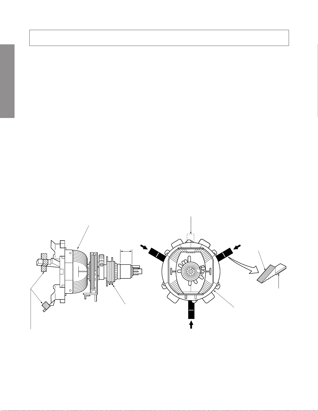
Note: The PURITY/CONVERGENCE MAGNET assembly and rubber wedges need mechanical positioning.
Refer to figure 1.
GENERAL ADJUSTMENTSSPECIFIC INFORMATIONS
*
COLOR PURITY ADJUSTMENT
NOTE : Before attempting any purity adjustments, the receiver
1. Demagnetize the picture tube and cabinet using a degauss-
2. Set the brightness and contrast to maximum.
3. Use a green raster from among the built-in test signals.
4. Loosen the clamp screw holding the yoke and slide the
Mounting position of the purity magnet assembly should fit to same position as old one because slightly difference to
the position depend on a kind of tube.
There are no adjustment of purity and convergence in some picture tube (Unified with purity magnet)
should be operated for at least fifteen minutes.
ing coil.
yoke backward or forward to provide vertical green belt
(zone) in the picture screen.
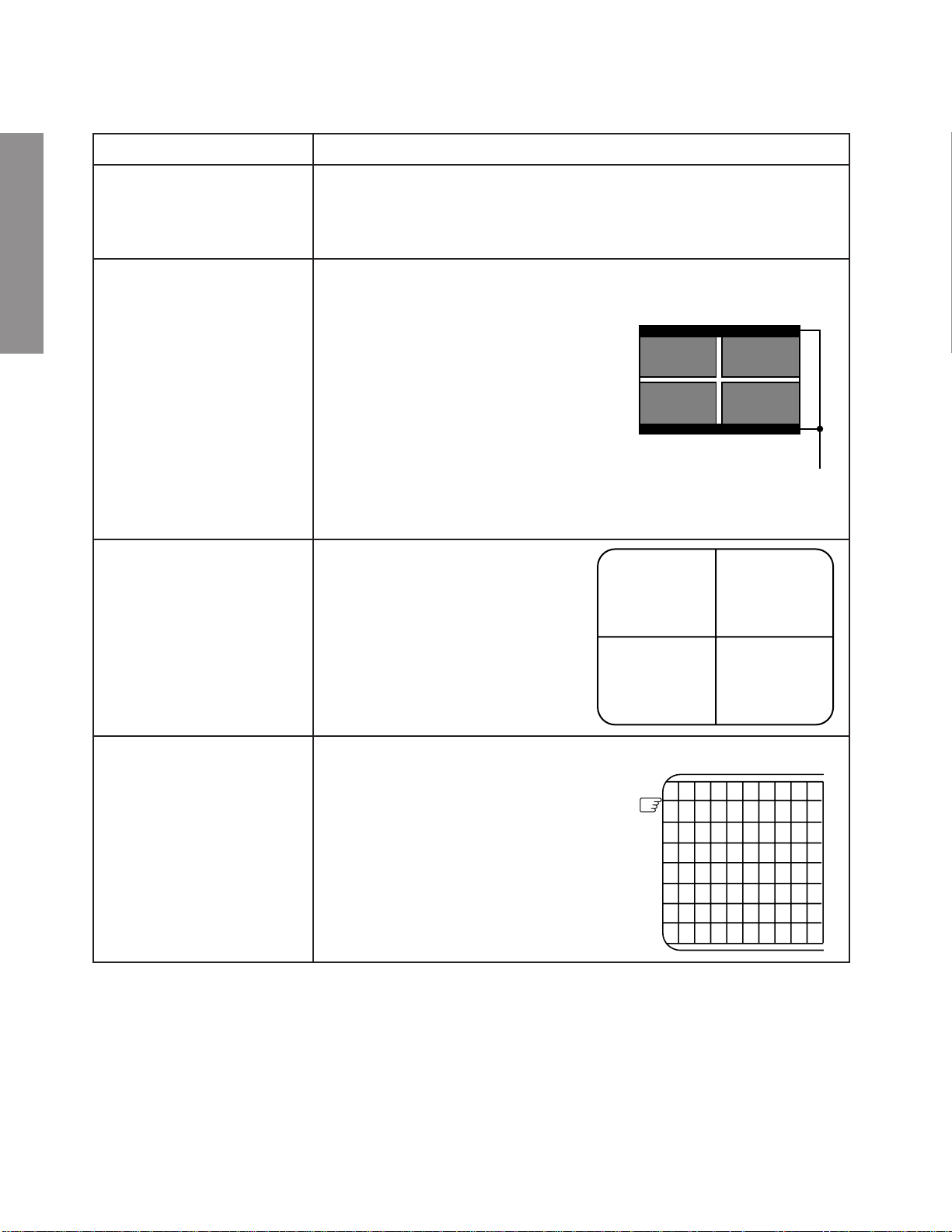
SET-UP ADJUSTMENT
5. Remove the Rubber Wedges.
6. Rotate and spread the tabs of the purity magnet (See figure 2.) around the neck of the picture tube until the green
belt is in the center of the screen. At the same time , enter
the raster vertically.
7. Slowly move the yoke forward or backward until a uniform
green screen is obtained. Tighten the clamp screw of the
yoke temporarily.
8. Check the purity of the red and blue raster.
GLASS CLOTH
TAPES
DEFLECTION
YOKE
29.1mm(28", 29")
25mm(25")
19mm(19", 20", 21")
14mm(13", 14")
PURITY/
CONVERGENCE
MAGNET ASS'Y
Figure 1.
TEMPORARY
MOUNTING
RUBBER WEDGE
ADHESIVE
DEFLECTION
YOKE
– 4 –
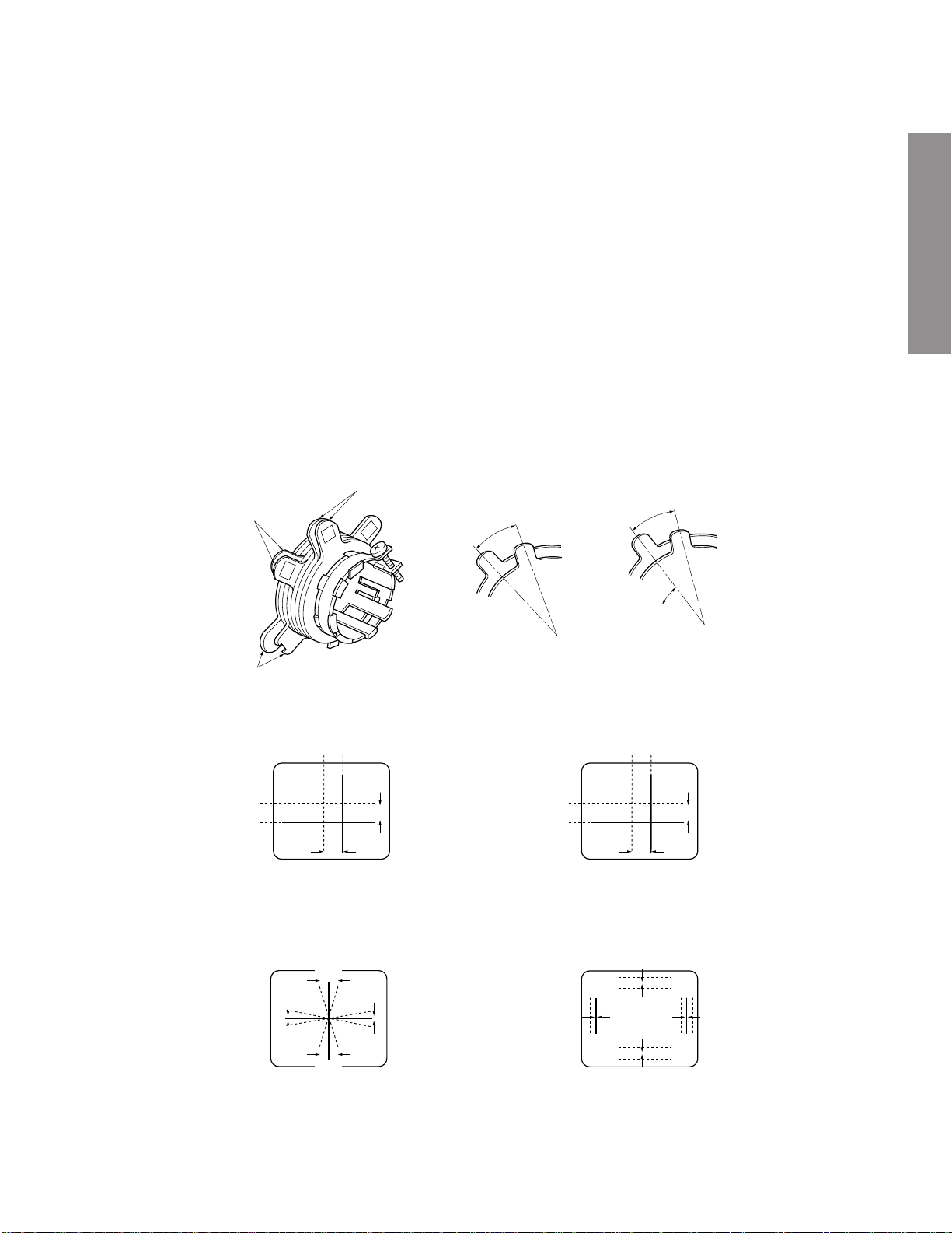
CONVERGENCE ADJUSTMENTS
NOTE: Before attempting any convergence adjustments, the
receiver should be operated for at least fifteen minutes.
■ CENTER CONVERGENCE ADJUSTMENT
1. Use the cross-dot pattern from among the built-in test signals.
2. Set the brightness and contrast for well defined pattern.
3. Adjust two tabs of the 4-Pole Magnets to change the angle between them (See figure 2.) and superimpose red
and blue vertical lines in the center area of the picture
screen.
4. Turn the both tabs at the same time keeping the angle
constant to superimpose red and blue horizontal lines at
the center of the screen.
5. Adjust two tabs of 6-Pole Magnets to superimpose red/
blue line and green one. Adjusting the angle affects the
vertical lines and rotating both magnets affects the horizontal lines.
6. Repeat adjustments 3, 4, 5 keeping in mind red, green
and blue movement, because 4-Pole Magnets and 6-Pole
Magnets have mutual interaction and make dot movement
complex.
6-POLE
4-POLE
MAGNETS
MAGNETS
ADJUST THE ANGLE
(VERTICAL LINES)
■ CIRCUMFERENCE CONVERGENCE ADJUSTMENT
1. Loosen the clamping screw of deflection yoke slightly to
allow the yoke to tilt.
2. Temporarily put a wedge as shown in figure 1. (Do not
remove cover paper on adhesive part of the wedge.)
3. Tilt front of the deflection yoke up or down to obtain better
convergence in circumference. (See figure 3.) Push the
mounted wedge into the space between picture tube and
the yoke to fix the yoke temporarily.
4. Put other wedge into bottom space and remove the cover
paper to stick.
5. Tilt front of the yoke right or left to obtain better convergence in circumference. (See figure 3.)
6. Keep the yoke position and put another wedge in either
upper space. Remove cover paper and stick the wedge
on picture tube to fix the yoke.
7. Detach the temporarily mounted wedge and put it in another upper space. Stick it on picture tube to fix the yoke.
8. After fixing three wedges, recheck overall convergence.
Tighten the screw firmly to fix the yoke and check the y oke
is firm.
9. Stick three adhesive tapes on wedges as shown in figure
1.
FIXED
GENERAL ADJUSTMENTSSPECIFIC INFORMATIONS
ROTATE TWO TABS
AT THE SAME TIME
(HORIZONTAL LINES)
PURITY
MAGNETS
CONVERGENCE MAGNET ASSEMBLY ADJUSTMENT OF MAGNETS
Figure 2.
BLU RED
BLU
RED
4-POLE MAGNETS MOVEMENT
BGR
R
G
B
RGB
RED/BLU
GRN
Center Convergence by Convergence Magnets
B
G
R
RED/BLU GRN
6-POLE MAGNETS MOVEMENT
B
G
R
BGR
RGB
R
G
B
INCLINE THE YOKE UP (OR DOWN)
Circumference Convergence by DEF Yoke
Figure 3. Dot Movement Pattern
INCLINE THE YOKE RIGHT (OR LEFT)
– 5 –
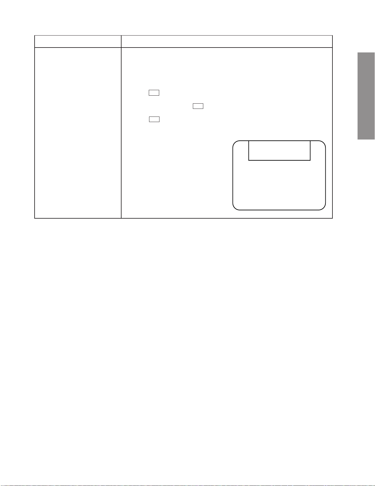
1. ENTERING TO SERVICE MODE
1) Press o button once on
Remote Control.
SERVICE MODE
2) Press o button again to
keep pressing.
3) While pressing the o button,
press MENU button on TV set.
Mute or
GENERAL ADJUSTMENTSSPECIFIC INFORMATIONS
2. DISPLAYING THE ADJUSTMENT MENU
1) Press MENU button on TV.
Adjustment mode
ITEM
DATA
3. KEY FUNCTION IN THE SERVICE MODE
The following key entry during display of adjustment menu provides special functions.
A single horizontal line ON/OFF: INFO button (on Remote) or a button (on TV)
Test signal selection : a button (on Remote)
Selection of the adjustment items : Channel s/t (on TV or Remote)
Change of the data value : Volume ; +/– (on TV or Remote)
Adjustment menu mode ON/OFF : MENU button (on TV)
Initialization of the memory (QA02) : CALL + Channel button on TV (s)
Reset the count of operating protect
circuit to “00”: CALL + Channel button on TV (t)
“RCUT” selection : 1 button
“GCUT” selection : 2 button
“BCUT” selection : 3 button
“CNTX” (or “SCNT”) selection : 4 button
“COLC” selection : 5 button
“TNTC” selection : 6 button
Self diagnostic display ON/OFF : 9 button
Item
Data
Press
Press
Item
Data
(Service mode display)
Service mode
S
S
Color thickness correction
note: Displayed differently as shown below, de-
pending on the setting of the receiving color
system.
COLP (PAL)
COLC (NTSC)
COLS (SECAM)
CAUTION : Never try to perform initialization unless you have changed the memory IC.
– 6 –
4. SELECTING THE ADJUSTING ITEMS
1) Every pressing of CHANNEL s button in the service mode changes the adjustment items in the order of table-2.
(t button for reverse order)
Refer to table-2 for preset data of adjustment mode.
(See SETTING & ADJUSTING DATA on page 18)
5. ADJUSTING THE DATA
1) Pressing of VOLUME ; +/– button will change the value of data in the range from 00H to FFH. The variable
range depends on the adjusting item.
6. EXIT FROM SERVICE MODE
1) Pressing POWER button to turn off the TV once.
■ INITIALIZATION OF MEMORY DATA OF QA02
After replacing QA02, the following initialization is required.
1. Enter the service mode, then select any register item.
2. Press and hold the CALL button on the Remote, then press the CHANNEL s button on the TV. The initialization of QA02 has
been complated.
3. Check the picture carefully. If necessary, adjust any adjustment item above.
Perform “Auto search Memory” on the owner’s manual.
CAUTION: Never attempt to initialize the data unless QA02 has been replaced.
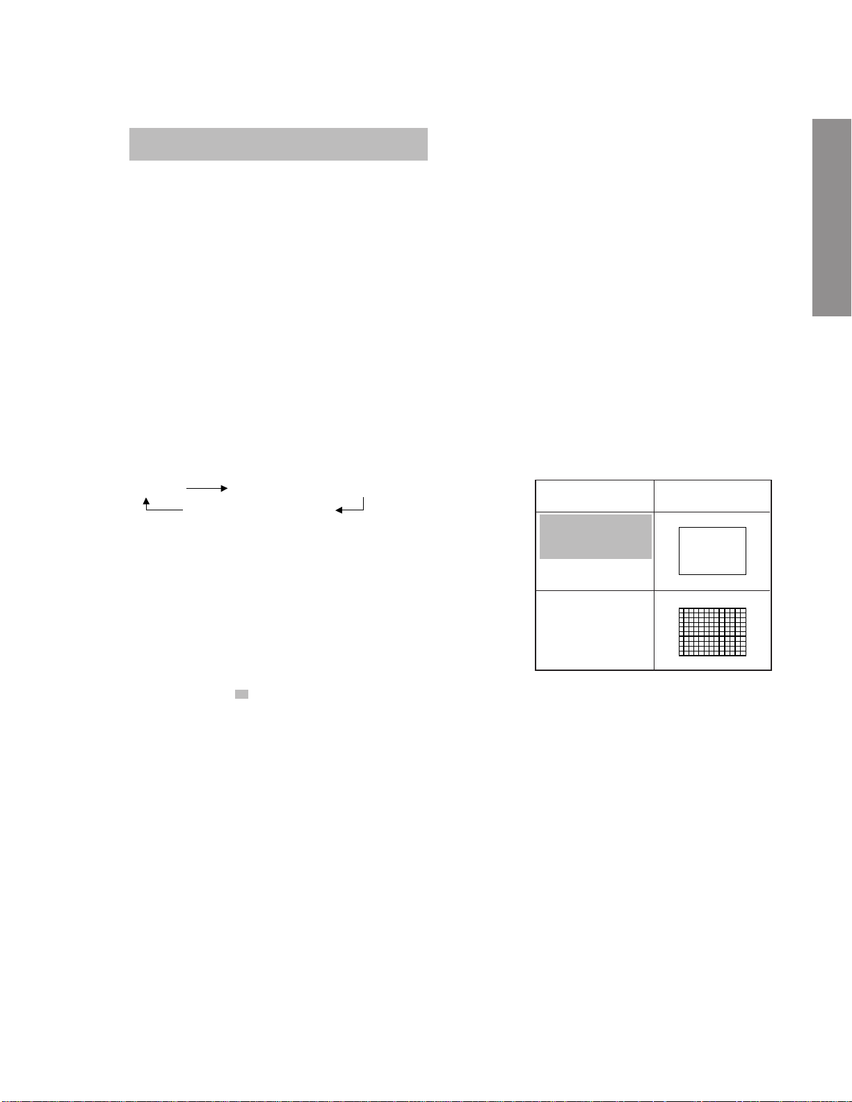
7. TEST SIGNAL SELECTION
1) Every pressing of a button on the Remote Control changes the built-in test patterns on screen as described below
in SERVICE MODE.
GENERAL ADJUSTMENTSSPECIFIC INFORMATIONS
Signal off
PAL signals (5 patterns)
The signals marked with are not usable to display in the Test signal for some model.
*
NTSC signals (5 patterns)
• Red raster
• Green raster
• Blue raster
• All White
• Black cross-hatch
Signals Picture
– 7 –

8. SELF DIAGNOSTIC FUNCTION
1) Press “9” button on Remote Control during display of adjustment menu in the service mode.
The diagnosis will begin to check if interface among IC’s are executed properly.
2) During diagnosis, the following displays are shown.
<SELF CHECK>
23******
1
POWER : 00
2
BUS LINE : OK
3
BUS CONT : OK
4
BLOCK :
5
GENERAL ADJUSTMENTSSPECIFIC INFORMATIONS
UV V1 V2 V3
QV01
Indicated color of mode now selected : Green and Red
Indicated color of other modes : White
Green :Normal
Red : The microcomputer operates to provide judgement
of no video signal. The red color is still indicated
though the signal is input, failure may exist in input
signal line including QV01.
QV01 : In case of indication green ---Normal
In case of indication red with input signal---Failure may exist in output line including QV01.
1 Part number of microcomputer (QA01)
2 Operation number of protecting circuit ----“00” is nor-
mal.
When indication is other than “00”, overcurrent apts to
flow, and circuit parts may possibly be damaged.
3 BUS LINE CHECK ----“OK” is normal.
“SDA1-GND” ------------- SDA-GND short circuit.
“SCL1-GND” -------------- SCL-GND short circuit.
“SCL1-SDA1” ------------- SCL-SDA short circuit.
4 BUS CONT ----“OK” is normal.
When indication shows “Q uuu NG”, the device with
the number may possibly be damaged.
5BLOCK
NOTE: Component which controls character display on
screen is ICF01 (TELETEXT IC.). If this display
function fails to operate due to damage in ICF01,
self diagnosis procedure is as follows.
(1) In case that power indicator is blinking with
interval of 0.5 seconds; it means protecting
circuit (Current limiter) is operating, and circuit components may possibly be damaged.
Check related components.
(2) In case that power indicator is blinking with
interval of 1 second; Protecting circuit does
not operate, but a part of Bus line does not
operate normally. Check Bus line.
UV : TV reception mode
V1: VIDEO 1 input mode (a1)
V2: VIDEO 2 input mode (a2)
V3: VIDEO 3 input mode (a3)
The items marked with are not usable to display in the SELF DIAGNOSTIC FUCTION for some model.
*
– 8 –

1. ENTERING TO DESIGN MODE
1) Select the Service mode.
DESIGN MODE
2) While pressing o or CALL button on
Remote and press MENU button on TV.
3) Press MENU button on TV.
S D
(Design mode) (Adjustment mode)
When QA02 is initialized, items “OPT0” and “OPT1” of DESIGN MODE are set to the data of the representative model of this
chassis family.
Therefore, because ON-SCREEN specification remains in the state of the representative of model. This model is required to
reset the data of items “OPT0” and “OPT1”.
2. SELECTING THE ADJUSTING ITEMS
Every pressing of CHANNEL t button in the design mode changes the adjustment items in the order of table-3.
(s button for reverse order)
Refer to table-3 for data of design mode.
(See SETTING & ADJUSTING DATA on page 18)
3. ADJUSTING THE DATA
Pressing of VOLUME s or t button will change the value of data.
Press
Press
ITEM
DATA
GENERAL ADJUSTMENTSSPECIFIC INFORMATIONS
– 9 –
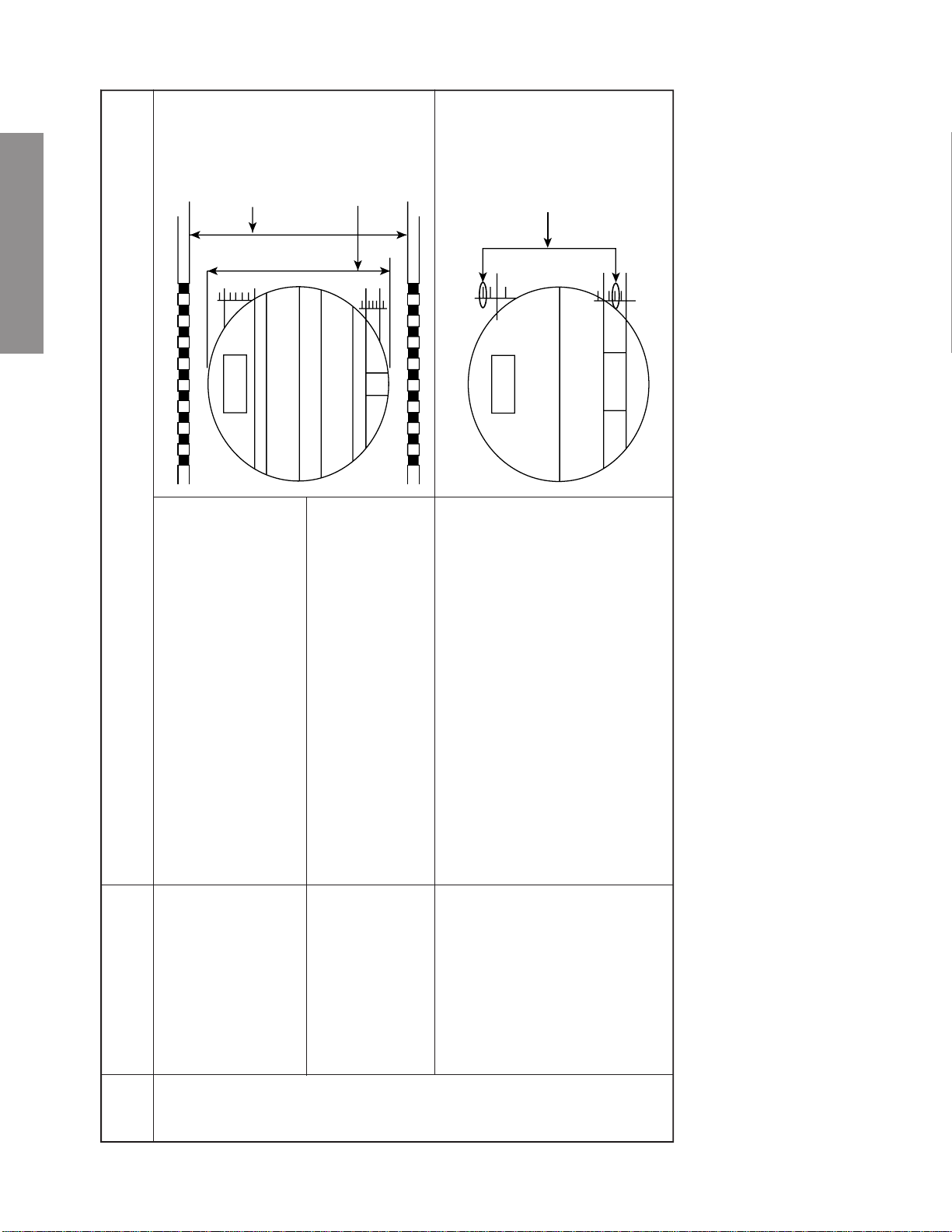
ELECTRICAL ADJUSTMENTS
ITEM ADJUSTMENT PROCEDURE
FOCUS VR ADJ
SUB-BRIGHTNESS
(BRTC)
GENERAL ADJUSTMENTSSPECIFIC INFORMATIONS
Note: Constrict the picture height
until the vertical retrace line
appears adjusting the item
HIT (HEIGHT).
HORIZONTAL POSITION
ADJUSTMENT (HPOS)
VERTICAL POSITION
ADJUSTMENT (VPOS)
1. Enter the service mode, then select any register item.
2. Press the TV/VIDEO button on the Remote until the black cross-bar pattern appears on the screen.
3. Adjust the FOCUS control (on T461) for well defined scanning lines on the picture
screen.
1. Set CONTRAST to minimum, and
BRIGHTNESS to center by adjusting
user controls.
2. Set the TV in service mode to get white
cross-bar of inside pattern.
3. Select BRTC (brightness correction),
and adjust the ; – /+ button to reduce
the value so that white portion of inside
pattern slightly light.
4. Adjust ; – /+ button to increase the
data value of BRTC, and set it just
before the difference between the belt of
vertical retrace and the border of black
portion of inside pattern is visible.
After that, return vertical height and
contrast.
1. Set the TV in service mode, and get
black or white cross-bar signal with
VIDEO button on remote hand unit.
2. Select either HPOS (Horizontal
picture phase) or VPOS (Vertical
picture phase) with CHANNEL s, t
buttons, and adjust horizontal or
vertical picture position in the center
of screen with VOLUME ; – /+
buttons.
Belt of vertical retrace
VERTICAL AMPLITUDE
ADJUSTMENT (HIT)
1. Set the TV in service mode, and get
black or white cross-hatch signal
with VIDEO button on remote hand
unit.
2. Select HIT (Vertical amplitude) with
CHANNEL s, t buttons, and adjust
vertical amplitude with VOLUME
; – /+ buttons so that vertical amplitude lacks a little.
3. Adjust vertical amplitude with VOLUME ; – /+ buttons so that the first
bar on cross-hatch signal touches
edge of screen.
– 10 –
The first
ITEM ADJUSTMENT PROCEDURE
WHITE BALANCE
ADJUSTMENT
CUTOFF ADJUSTMENT
•
(RCUT)
(GCUT)
(BCUT)
DRIVE ADJUSTMENT
•
(GDRV)
(BDRV)
1. Set Contrast to 40, and brightness to +20 by picture control.
2. Set the TV in service mode, and get the inside W/B adjusting signal with VIDEO
button.
3. Select RCUT, GCUT and BCUT with CHANNEL s, t buttons, to set individual
values to Initial reference data, and to set GDRV and BDRV to Initial reference
data with VOLUME ; – /+ buttons (See page 18).
4. Press -/- - button on the remote control and rotate Screen VR to get one slight
horizontal line on screen.
Note: Every pressing of -/- - button provides Horizontal line picture and Normal
picture alternately.
5. Press -/- - button to release horizontal line picture, and select the two other colors
which did not light in the above step with CHANNEL s, t buttons . Then tap VOLUME ; – /+ buttons so that three colors slightly light in the same level.
X To correct white balance in light area,
select GDRV and BDR V with CHANNEL
s, t buttons to adjust.
X To correct white balance in dark area,
perform fine adjustment of RCUT , GCUT
and BCUT.
Light area check
(to show white)
Dark area check
(to show black)
GENERAL ADJUSTMENTSSPECIFIC INFORMATIONS
– 11 –

)
2
)
2
GENERAL ADJUSTMENTSSPECIFIC INFORMATIONS
2.5 ± 0.1 Vp-p
4±1.5 pieces
level to the white peak.
y Adjust the amplitude from the pedestal
y Adjust the number of collapsed black lines
TP46B
Screen adjust-
1.2 ± 0.1 Vo-p
Bright part
Screen adjustment
(103cd/m
of the sub-bright signal.
(Be sure to apply Y mute during adjustment)
x To adjust after W/B, [SCNT] adjustment.
y Adjust the amplitude of B-Y.
y Enter Horizontal Straight-line Mode.
x Gradually increase the screen VR until R,
TP46B
ment
Screen adjustment
8750K-0.002uv
Dark part
(17cd/m
8750K-0.002uv
G, or B line starts to light up slightly.
sition here.
c Deter mine the screen VR adjustment po-
v Gradually increase remaining two screen
Screen judgment
(CA100)
VRs – except the line that lit up as men-
tioned in item x above – until respective
line starts to light up slightly. (Adjust until
the screen becomes almost white.)
correct value is set to both the dark and
bright parts.
b Exit from Horizontal Straight-line Mode.
n Using CA100, repeat this adjustment until
Input signals Measuring points Adjusting methods Adjusting standards
Settings
(User control)
Items Names
(Reference Factory Adjustments)
Sub-bright signal
(PAL-I Signal)
Sub-bright Signal
Dynamic MODE
Screen size: WIDE
Audio system: I
Dynamic MODE
Screen size: WIDE
Sub-contrast
[SCNT]
Sub-bright
[BRTC]
Center
Sub-bright Signal
(PAL)
Dynamic MODE
Screen size: Dynamic
MODE
Screen size: WIDE
[RCUT]: 40
[GCUT]: 40
Sub-color center
PAL
R Cutoff
G Cutoff
B Cutoff
[COLP]
SCREEN
VR
[RCUT]
– 12 –
[BCUT]: 40
[GDRV]: 40
G Drive
B Drive
[GCUT]
[BCUT]
[GDRV]
[BDRV]: 40
[BDRV]

0 ± 10 mV
0 ± 10 mV
1.6 ± 0.1 Vo-p
(Pedestal to Peak)
GENERAL ADJUSTMENTSSPECIFIC INFORMATIONS
chrome signal part aligns with that of BLK.
y Vary [SBY] so that the level of mono-
TP01
Input signals Measuring points Adjusting methods Adjusting standards
SECAM Color bar
Settings
(User control)
chrome signal part aligns with that of BLK.
y Vary [SRY] so that the level of mono-
TP02
SECAM Color bar
(Be sure to apply Y mute during adjust-
ment)
y Adjust the amplitude of B-Y.
TP46B
SECAM Color bar
Items Names
SECAM
B-Y Black
level
[SBY]
– 13 –
SECAM
R-Y Black
level
[SRY]
Dynamic MODE
Screen size: WIDE
Sub-color
Center
SECAM
[COLS]
GENERAL ADJUSTMENTSSPECIFIC INFORMATIONS
Contact point
during WIDE
mode
Contact point
during Super-
live mode
Nero
Contact point
during CIN-
EMA mode
Yellow Red Yellow
PAL WG Phillips Pattern, User adjustment standard
Adjust the vertical amplitude by [HIT] so that both upper and
Adjusting items Adjusting methods
Vertical amplitude [HIT]
1. Data adjustment
Vertical WIDE mode
lower flags will disappear from the screen.
PAL Phillips Pattern, User adjustment standard
Adjust the vertical position [VPS1] with Phillips Pattern so
that the vertical screen position will come to the center (see
the right sketch).
PAL Phillips Pattern, User adjustment standard
Adjust the vertical amplitude by [HIT] so that the top and
bottom of the circle will touch the CPT mask with Philips
Pattern (see the right sketch).
Vertical position [VPS1]
Super-live mode
Vertical amplitude [HIT]
Phillips Pattern, User adjustment standard
Adjust the vertical amplitude by [HIT] so that the points
shown in the right bottom sketch will touch the CRT mask
(see the right sketch).
CINEMA mode
Vertical amplitude [HIT]
– 14 –
Conditions:
PAL Retoma signal
WIDE mode, User adjustment standard
Adjustment:
Set it at the position, where the screen center becomes optimum focus and most counterclockwise,
using the focus volume (F1) of the fly-back transformer (T461).
Conditions:
PAL Retoma signal
WIDE mode, User adjustment standard
Adjustment:
Set it at the position, where the screen center becomes optimum focus and most counterclockwise,
using the focus volume (F2) of the fly-back transformer (T461).
Conditions:
PAL WG Phillips Pattern
WIDE mode, User adjustment standard
Adjustment:
Use [VPS1] and make adjustments so that the upper and lower positions will touch the mask.
(Adjust and orient CPT either toward the south or north. If this is impossible, offset the difference.)
GENERAL ADJUSTMENTSSPECIFIC INFORMATIONS
Focus adjustment (1)
HOR. FOCUS
All models
1
No. Target model names Adjusting items Adjusting methods
2. Circuit adjustment (Volume/data adjustment)
Focus adjustment (2)
VERT.FOCUS
Vertical position adjustment
All models
2
– 15 –
GENERAL ADJUSTMENTSSPECIFIC INFORMATIONS
(a) (b) (c) (d)
Adjustment methods
distortion shown in Fig. (b).
adjustments, make adjustments by using the data of [CNR], [CPAR],
and [CSAW].
1 Decrease [CPAR] in case of the distortion shown in Fig. (a). On the contrary, increase [CPAR] in case of the
distortion shown in Fig. (d).
2 Decrease [CSAW] in case of the distortion shown in Fig. (c). On the contrary, increase [CSAW] in case of the
Use PAL WG Phillips Pattern and adjust the horizontal amplitude to fit the mask to the frames of left and right flags in
WIDE mode.
Adjustment items
WIDE mode
(During 4:3)
3. Data Adjustment
Horizontal
Use PAL WG Phillips Pattern and adjust so that the side-pin and trapezoidal distortions become optimum in WIDE mode.
Use the horizontal phase [HPOS] for the horizontal screen position, and make adjustments so that the position will
become a center.
Horizontal phase: [HPOS]
Horizontal amplitude: [WIDE]
Side DPC: [PARA]
• Note: In case distortion adjustment is insufficient by the [PARA] [TRAP]
Check and confirm the side-pin at the mode of 4:3.
(If necessary, examine the grade of side panel at the mode of 4:3 and reconfirm)
Trapezoidal distortion: [TRAP]
Corner distortion: [CNR]
Center warp: [CPAR]
Parallelogram distortion: [CSAW]
Use PAL Phillips Pattern and fit the frames of the left and right flags to the mask in Super-live and WIDE modes.
Make adjustments to achieve optimum side-pin distortion and trapezoidal distortion.
Super-live mode
Horizontal amplitude: [WIDE]
Side DPC: [PARA]
– 16 –
If any further adjustment is required, use the horizontal phase [HPOS] and corner distortion [CNR] for adjustment.
Trapezoidal distortion: [TRAP]
Use PAL Phillips Pattern and adjust the horizontal amplitude to fit the mask to the frames of left and right flags in CINEMA
mode.
Horizontal phase [HPOS]
Corner distortion: [CNR]
CINEMA mode
Horizontal amplitude: [WIDE]
Make adjustments to achieve optimum side-pin distortion and trapezoidal distortion.
If any further adjustment is required, use the horizontal phase [HPOS] and corner distortion [CNR] for adjustment.
Side DPC: [PARA]
Trapezoidal distortion: [TRAP]
Horizontal phase: [HPOS]
Corner distortion: [CNR]

CIRCUIT CHECK
HIGH VOLTAGE CHECK
CAUTION: There is no HIGH VOLTAGE ADJUSTMENT on this chassis. Checking should be done following the steps
below.
1. Connect an accurate high voltage meter to the second anode of the picture tube.
2. Turn on the receiver. Set the BRIGHTNESS and CONTRAST controls to minimum (zero beam current).
3. High voltage must be measured below (B) kV.
Refer to table-1 for high voltage (B).
(See SETTING & ADJUSTING DATA on page 18)
4. Vary the BRIGHTNESS control to both extremes to be sure the high voltage does not e xceed the limit under any conditions.
GENERAL ADJUSTMENTSSPECIFIC INFORMATIONS
– 17 –
CHAPTER 2 SPECIFIC INFORMATIONS
SAFETY INSTRUCTIONS
GENERAL ADJUSTMENTSSPECIFIC INFORMATIONS
SERVICE MODE
ADJUSTING ITEMS AND DATAS IN THE SERVICE MODE:
SETTING & ADJUSTING DATA
32”
HIGH VOLTAGE AT ZERO BEAM: (A) 33.2 kV
MAX HIGH VOLTAGE: (B) 34.0 kV
AV VOL T AGE
Table-1
(C) 220~240 V
Item
RCUT
GCUT
BCUT
GDRV
BDRV
CNTX
BRTC
COLC
TNTC
COLP
COLS
COLD
SCNT
R CUTOFF (B/W)
G CUTOFF (B/W)
B CUTOFF (B/W)
R DRIVE
B DRIVE
SUB CONTRAST MAX
SUB BRIGHT CEN
SUB COLOR CEN NTSC
SUB TINT CEN
SUB COLOR CEN PAL
SUB COLOR CEN SECAM
SUB COLOR CEN DTV
SUB CONTRAST
DESIGN MODE
ADJUSTING ITEMS AND DATAS IN THE DESIGN MODE:
Adjustment
Item Name of adjustment
* There are no adjusting item in the DESIGN MODE.
Reference data
40H
40H
40H
35H
35H
7FH
80H
00H
20H
3DH
3DH
3DH
08H
Item
SRY
SBY
HPOS
VPOS
HIT
VLIN
VSC
VPS2
WID
PARA
CNR
TRAP
VFC
Table-2
Preset Data
Adjustment
SECAM R-Y
SECAM B-Y
50Hz H-POSITION
V-POSITION
HEIGHT
V-LINEARITY
V-S CORRECTION
V-SHIFT
PICTURE WIDTH
E-W PARABOLA
E-W CORNER
TRAPEZIUM
V-F CORRECTION
Data
Reference data
08H
08H
67H
00H
38H
12H
23H
40H
2CH
1CH
10H
4BH
0FH
Remarks
Table-3
– 18 –
Front
HEAD
PHONE
(VIDEO-3)
S-VIDEO TERMINAL
VIDEO-3
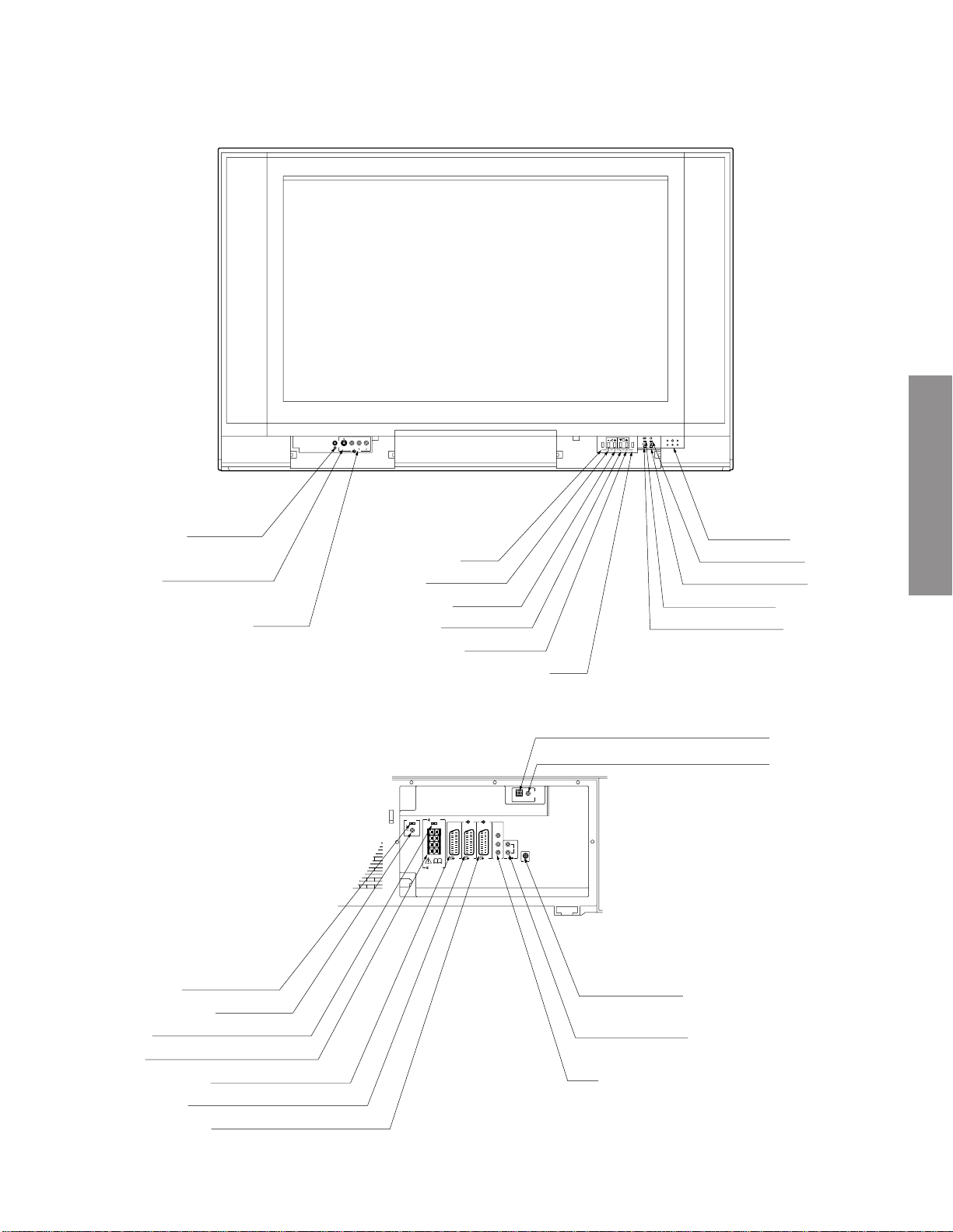
LOCATION OF CONTROLS
S-VIDEO VIDEO L/MONO
R
AUDIO
(3)
MENU
VOLUME DOWN
VOLUME UP
POSITION DOWN
POSITION UP
EXIT
MENU EXIT
GENERAL ADJUSTMENTSSPECIFIC INFORMATIONS
P
MAIN SWITCH
POWER INDICATOR
ON-TIMER INDICATOR
STEREO INDICATOR
BILINGUAL INDICATOR
Rear terminals
WOOFER SWITCH
WOOFER OUT
EXTERNAL SPEAKER SWITCH
EXTERNAL SPEAKER TERMINAL
VIDEO-1 (21PINS FULL)
VIDEO-2 (21PINS S-VIDEO/AV)
VIDEO-3 (21PINS S-VIDEO/AV)
DIGITAL AUDIO INPUT (OPTICAL)
DIGITAL AUDIO INPUT (COAXIAL)
DIGITAL
AUDIO
INPUT
OPTICAL COAXIAL
PCM / DOLBY DIGITAL
MAIN (8Ω)
WOOFER
EXT INTEXT INT
R
(+)
(-)
(-)
(+)
R
SURROUND
(8Ω)
3S 3S
(S-VIDEO)(S-VIDEO)
L
(+)
(-)
(-)
(+)
L
Y
B
C
L
AUDIO
CR
R
DVD
(3)
(2)(1)
COMP.
(AUDIO / VIDEO)(AUDIO / VIDEO)
(FIXED)
AERIAL TERMINAL
AUDIO OUT (FIXED)
DVD
– 19 –
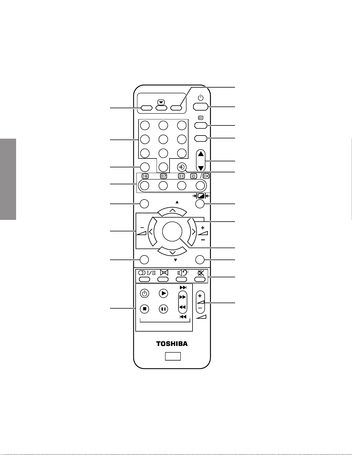
Remote Controller
SIZE Button
GENERAL ADJUSTMENTSSPECIFIC INFORMATIONS
Keypad Number Buttons
INFO Buttons
NexTView Buttons
Menu Control Buttons
MENU Buttons
Teletext
F
F
1 2 3
4 5 6
SIZE
CALL
TEXT
TV
Power ON/ OFF
CALL
Teletext
7 8 9
INFO.
0
P
•Programme Position up/down
VIDEO (+F)
NexTView
P
Picture Controls
Menu Control Buttons
ENTER
MENU EXIT
P
ENTER
EXIT
Video Recoder/DVD Buttons
to operate your Toshiba
Video Recorder & DVD
VTR / DVD
VTR / DVD
•Stereo/Bilingual
•Sound Mute
Volume
– 20 –
~
~
–+
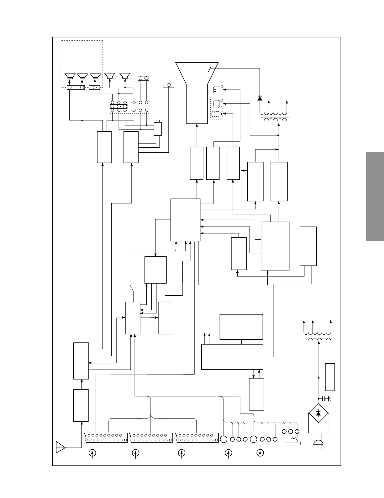
TUNER IF/MPX/APRO
H001
QA01
QA02
Q801
H002
QV01
L/R
C/S
TV-L/R
QF02
AV SW
EPG-TEXT
21PIN
(FULL)
21PIN
(3)
(FRONT)
(3)
(REAR)
MEMORY
µ-CON
I
2
C BUS
HYBRID
DIGITAL
IN
CONVERTER TRANS.
+B VOLTAGE
AUTO
LIVE UNIT
RGB
DIGI-COMB
& MCD
QZ01, Q501
QF01
Y
C
VYC
Y
RGB
C
CHROMA
VIDEO
DEF.
Q501
Q302
Q4420
VIDEO OUT
VM
V. OUT
H. OUT
EW 100Hz
F.B.T.
H.V.
D.Y.
V
H
CRT
Q301
Q404
DPC
Q901,Q903,Q905
(1)
(2)
21PIN
(S+AV)
(3)
**
*
*
*
*
*
I
2
C BUS CONTROL
S
V
L
R
S
V
L
R
S
HEAD PHONE
EXT/INT
SPK SW
Q670
AUDIO OUT
Q640
AUDIO OUT
SURROUND
R
SURROUND
L
EXT SPK
L
R
CENTRE
EXT SPK
WOOFER
TERM
QK01, QK05
QR01
SUB
µ-CON
DIG-FRAME
SCAN
QX01, QX02
CIRCUIT BLOCK DIAGRAM
GENERAL ADJUSTMENTSSPECIFIC INFORMATIONS
– 21 –
CHASSIS AND CABINET REPLACEMENT PARTS LIST
WARNING: BEFORE SERVICING THIS CHASSIS, READ THE “X-RAY RADIATION PRECAUTION”, “SAFETY
PRECAUTION” AND “PRODUCT SAFETY NOTICE” ON PAGE 3 OF THIS MANUAL.
CAUTION: The international hazard symbols “ ” in the schematic diagram and the parts list designate com-
ponents which have special characteristics important for safety and should be replaced only with types identical to
those in the original circuit or specified in the parts list. The mounting position of replacements is to be identical
with originals. Before replacing any of these components, read carefully the PRODUCT SAFETY NOTICE. Do not
degrade the safety of the receiver through improper servicing.
NOTICE:
•
The part number must be used when ordering parts, in order to assist in processing, be sure to include the Model
number and Description.
•
The PC board assembly with * mark is no longer available after the end of the production.
GENERAL ADJUSTMENTSSPECIFIC INFORMATIONS
Capacitors ............. CD : Ceramic Disk PF : Plastic Film EL : Electrolytic
Resistors ............... CF : Carbon Film CC : Carbon Composition MF : Metal Film
(All CD and PF capacitors are ±5%, 50V and all resistors, ±5%, 1/6W unless otherwise noted.)
Models : 32ZD08G, 32ZD08B
OMF : Oxide Metal Film VR : Variable Resistor FR : Fusible Resistor
Location
No.
CAPACITORSCAPACITORS
CAPACITORS
CAPACITORSCAPACITORS
C102 24763221 EL, 220?F, ±20%, 16V
C105 24212102 CD, 1000pF, ±10%
C106 24797100 EL, 10?F, ±20%, 50V
C108 24794221 EL, 220?F, ±20%, 16V
C109 24232103 CD, 0.01?F, +80%, -20%
C110 24797479 EL, 4.7?F, ±20%, 50V
C110 24797229 EL, 2.2?F, ±20%, 50V
C111 24797220 EL, 22?F, ±20%, 50V
C111 24797229 EL, 2.2?F, ±20%, 50V
C115 24232103 CD, 0.01?F, +80%, -20%
C201 24567104 PF, 0.1?F
C202 24232103 CD, 0.01?F, +80%, -20%
C203 24567104 PF, 0.1?F
C204 24797010 EL, 1?F, ±20%, 50V
C205 24797229 EL, 2.2?F, ±20%, 50V
C206 24797220 EL, 22?F, ±20%, 50V
C214 24567334 PF, 0.33?F
C215 24436101 CD, 100pF
C219 24436100 CD, 10pF
C220 24436100 CD, 10pF
C221 24436100 CD, 10pF
C229 24092398 CD, 0.1?F, +80%, -20%, 25V
C230 24232103 CD, 0.01?F, +80%, -20%
C232 24092398 CD, 0.1?F, +80%, -20%, 25V
C261 24794101 EL, 100?F, ±20%, 16V
C262 24232103 CD, 0.01?F, +80%, -20%
C263 24794470 EL, 47?F, ±20%, 16V
C264 24794100 EL, 10?F, ±20%, 16V
C302 24214471 CD, 470pF, ±10%, 500V
C303 24214471 CD, 470pF, ±10%, 500V
C305 24795222 EL, 2200?F, ±20%, 25V
C308 24797221 EL, 220?F, ±20%, 50V
C310 24795222 EL, 2200?F, ±20%, 25V
C313 24082057 PF, 0.22?F, 100V
C314 24793101 EL, 100?F, ±20%, 10V
C315 24212222 CD, 2200pF, ±10%
Part No. Description
(32ZD08G)
(32ZD08B)
(32ZD08G)
(32ZD08B)
Location
No.
C315 24797478 EL, 0.47?F, ±20%, 50V
C316 24795221 EL, 220?F, ±20%, 25V
C318 24794471 EL, 470?F, ±20%, 16V
C320 24795221 EL, 220?F, ±20%, 25V
C321 24567224 PF, 0.22?F
C322 24617915 EL, 1?F, ±10%, 50V
C323 24567474 PF, 0.47?F
C325 24590223 PF, 0.022?F
C326 24797010 EL, 1?F, ±20%, 50V
C327 24794471 EL, 470?F, ±20%, 16V
C329 24567224 PF, 0.22?F
C332 24212102 CD, 1000pF, ±10%
C341 24567474 PF, 0.47?F
C366 24082049 PF, 0.047?F, 100V
C370 24794100 EL, 10?F, ±20%, 16V
C371 24797100 EL, 10?F, ±20%, 50V
C372 24797470 EL, 47?F, ±20%, 50V
C373 24797470 EL, 47?F, ±20%, 50V
C390 24567474 PF, 0.47?F
C391 24567474 PF, 0.47?F
C392 24567474 PF, 0.47?F
C393 24567474 PF, 0.47?F
C401 24232103 CD, 0.01?F, +80%, -20%
C403 24590223 PF, 0.022?F
C404 24797229 EL, 2.2?F, ±20%, 50V
C410 24092341 CD, 470pF, ±10%, 2kV
C413 24214332 CD, 3300pF, ±10%, 500V
C416 24668101 EL, 100?F, ±20%, 35V
C417 24214391 CD, 390pF, ±10%, 500V
C419 24212102 CD, 1000pF, ±10%
C420 24794101 EL, 100?F, ±20%, 16V
C421 24567104 PF, 0.1?F
C423 24829623 PF, 0.063?F, 400V
C424 24794101 EL, 100?F, ±20%, 16V
C425 24794101 EL, 100?F, ±20%, 16V
C430 24232103 CD, 0.01?F, +80%, -20%
C430 24820392 PF, 0.0036?F, 630V
C431 24232103 CD, 0.01?F, +80%, -20%
C431 24794101 EL, 100?F, ±20%, 16V
C440 24082941 PF, 3000pF, ±3%, 1500V
C442 24082639 PF, 0.12?F, 400V
Part No. Description
– 22 –

Location
No.
Part No. Description
Location
No.
Part No. Description
C443 24082638 PF, 0.11?F, 400V
C444 24082830 PF, 3000pF, ±3%, 1800V
C445 24828473 PF, 0.047?F, 200V
C446 24679330 EL, 33?F, ±20%, 250V
C447 24829183 PF, 0.018?F, 400V
C448 24640908 EL, 33?F, ±20%, 160V
C461 24082834 PF, 4300pF, ±3%, 1800V
C462 24794222 EL, 2200?F, ±20%, 16V
C463 24212392 CD, 3900pF, ±10%
C464 24640872 EL, 10?F, ±20%, 100V
C470 24794470 EL, 47?F, ±20%, 16V
C471 24590473 PF, 0.047?F
C472 24567474 PF, 0.47?F
C473 24669010 EL, 1?F, ±20%, 50V
C475 24095887 PF, 0.01?F, ±3%, 630V
C476 24794220 EL, 22?F, ±20%, 16V
C477 24590102 PF, 1000pF
C479 24214471 CD, 470pF, ±10%, 500V
C481 24085988 EL, 1.0?F, ±20%, 50V,
Non-Polar
C482 24212152 CD, 1500pF, ±10%
C490 24082983 PF, 1.5?F, 250V
C492 24829473 PF, 0.047?F, 400V
C494 24082637 PF, 0.1?F, 400V
C495 24092343 CD, 680pF, ±10%, 2kV
C496 24092343 CD, 680pF, ±10%, 2kV
C501 24092293 Chip, 0.1?F, +80%, -20%, 25V
C502 24092293 Chip, 0.1?F, +80%, -20%, 25V
C502 24232103 CD, 0.01?F, +80%, -20%
C503 24794221 EL, 220?F, ±20%, 16V
C503 24794470 EL, 47?F, ±20%, 16V
C504 24814103 Chip, 0.01?F, +80%, -20%
C505 24794470 EL, 47?F, ±20%, 16V
C506 24814103 Chip, 0.01?F, +80%, -20%
C507 24092293 Chip, 0.1?F, +80%, -20%, 25V
C508 24092293 Chip, 0.1?F, +80%, -20%, 25V
C508 24797010 EL, 1?F, ±20%, 50V
C509 24092293 Chip, 0.1?F, +80%, -20%, 25V
C509 24794101 EL, 100?F, ±20%, 16V
C510 24794101 EL, 100?F, ±20%, 16V
C510 24797479 EL, 4.7?F, ±20%, 50V
C511 24092293 Chip, 0.1?F, +80%, -20%, 25V
C511 24232103 CD, 0.01?F, +80%, -20%
C512 24092293 Chip, 0.1?F, +80%, -20%, 25V
C513 24092293 Chip, 0.1?F, +80%, -20%, 25V
C513 24232103 CD, 0.01?F, +80%, -20%
C514 24567104 PF, 0.1?F
C514 24794470 EL, 47?F, ±20%, 16V
C515 24567104 PF, 0.1?F
C515 24814103 Chip, 0.01?F, +80%, -20%
C516 24774100 Chip, 10pF, ±0.5pF, CH
C517 24797478 EL, 0.47?F, ±20%, 50V
C518 24436101 CD, 100pF
C518 24814103 Chip, 0.01?F, +80%, -20%
C519 24092293 Chip, 0.1?F, +80%, -20%, 25V
C520 24212102 CD, 1000pF, ±10%
C520 24797229 EL, 2.2?F, ±20%, 50V
C521 24212102 CD, 1000pF, ±10%
C521 24567223 PF, 0.022?F
C522 24814103 Chip, 0.01?F, +80%, -20%
C525 24567104 PF, 0.1?F
C555 24092398 CD, 0.1?F, +80%, -20%, 25V
C556 24797010 EL, 1?F, ±20%, 50V
C608 24762222 EL, 2200?F, ±20%, 10V
C613 24794471 EL, 470?F, ±20%, 16V
C615 24085960 EL, 4.7?F, ±20%, 50V,
Non-Polar
C616 24590183 PF, 0.018?F
C617 24590102 PF, 1000pF
C618 24590823 PF, 0.082?F
C619 24794221 EL, 220?F, ±20%, 16V
C620 24794101 EL, 100?F, ±20%, 16V
C631 24567474 PF, 0.47?F
C631 24797010 EL, 1?F, ±20%, 50V
C632 24797100 EL, 10?F, ±20%, 50V
C632 24797479 EL, 4.7?F, ±20%, 50V
C633 24591124 PF, 0.12?F
C633 24781102 Chip, 1000pF, SL
C634 24206100 EL, 10?F, ±20%, 50V
C634 24668471 EL, 470?F, ±20%, 35V
C635 24814103 Chip, 0.01?F, +80%, -20%
C636 24206100 EL, 10?F, ±20%, 50V
C637 24765221 EL, 220?F, ±20%, 35V
C638 24814103 Chip, 0.01?F, +80%, -20%
C639 24590103 PF, 0.01?F
C640 24797220 EL, 22?F, ±20%, 50V
C641 24206100 EL, 10?F, ±20%, 50V
C641 24669010 EL, 1?F, ±20%, 50V
C642 24206478 EL, 0.47?F, ±20%, 50V
C643 24781102 Chip, 1000pF, SL
C644 24797010 EL, 1?F, ±20%, 50V
C645 24795470 EL, 47?F, ±20%, 25V
C647 24591102 PF, 1000pF
C648 24591102 PF, 1000pF
C649 24797229 EL, 2.2?F, ±20%, 50V
C650 24668102 EL, 1000?F, ±20%, 35V
C651 24668471 EL, 470?F, ±20%, 35V
C652 24668471 EL, 470?F, ±20%, 35V
C654 24591124 PF, 0.12?F
C655 24591124 PF, 0.12?F
C656 24232103 CD, 0.01?F, +80%, -20%
C657 24797229 EL, 2.2?F, ±20%, 50V
C661 24797478 EL, 0.47?F, ±20%, 50V
C662 24797229 EL, 2.2?F, ±20%, 50V
C663 24797229 EL, 2.2?F, ±20%, 50V
C665 24797010 EL, 1?F, ±20%, 50V
C666 24797010 EL, 1?F, ±20%, 50V
C667 24212102 CD, 1000pF, ±10%
C667 24797229 EL, 2.2?F, ±20%, 50V
C668 24212102 CD, 1000pF, ±10%
C668 24590102 PF, 1000pF
C669 24797330 EL, 33?F, ±20%, 50V
C670 24797330 EL, 33?F, ±20%, 50V
C670 24814103 Chip, 0.01?F, +80%, -20%
C671 24797100 EL, 10?F, ±20%, 50V
C671 24814103 Chip, 0.01?F, +80%, -20%
C672 24795470 EL, 47?F, ±20%, 25V
C672 24814103 Chip, 0.01?F, +80%, -20%
C673 24781102 Chip, 1000pF, SL
C673 24795470 EL, 47?F, ±20%, 25V
C674 24781102 Chip, 1000pF, SL
C674 24797100 EL, 10?F, ±20%, 50V
C675 24795470 EL, 47?F, ±20%, 25V
C677 24590102 PF, 1000pF
C677 24814103 Chip, 0.01?F, +80%, -20%
C678 24590102 PF, 1000pF
C678 24781102 Chip, 1000pF, SL
C679 24781102 Chip, 1000pF, SL
GENERAL ADJUSTMENTSSPECIFIC INFORMATIONS
– 23 –

Location
No.
Part No. Description
Location
No.
Part No. Description
C680 24668102 EL, 1000?F, ±20%, 35V
C681 24668102 EL, 1000?F, ±20%, 35V
C681 24781102 Chip, 1000pF, SL
C682 24668102 EL, 1000?F, ±20%, 35V
C682 24781102 Chip, 1000pF, SL
C685 24591124 PF, 0.12?F
C687 24232103 CD, 0.01?F, +80%, -20%
C688 24794220 EL, 22?F, ±20%, 16V
C689 24591124 PF, 0.12?F
C704 24591822 PF, 8200pF
C705 24797229 EL, 2.2?F, ±20%, 50V
C707 24794470 EL, 47?F, ±20%, 16V
GENERAL ADJUSTMENTSSPECIFIC INFORMATIONS
C712 24794470 EL, 47?F, ±20%, 16V
C713 24790100 EL, 10?F, ±20%, 160V
C714 24436101 CD, 100pF
C715 24214472 CD, 4700pF, ±10%, 500V
C716 24436101 CD, 100pF
C717 24214472 CD, 4700pF, ±10%, 500V
C718 24794470 EL, 47?F, ±20%, 16V
C719 24435151 CD, 150pF, 500V, SL
C720 24790100 EL, 10?F, ±20%, 160V
C721 24794470 EL, 47?F, ±20%, 16V
C805 24092281 CD, 4700pF, ±20%, AC250V
C806 24092281 CD, 4700pF, ±20%, AC250V
C808 24667331 EL, 330?F, ±20%, 25V
C810 24086063 EL, 330?F, ±20%, 400V
C810 24763102 EL, 1000?F, ±20%, 16V
* C813 24092555 CD, 1000pF, ±20%, AC250V
* C814 24092555 CD, 1000pF, ±20%, AC250V
C817 24092339 CD, 330pF, ±10%, 2kV
C818 24095931 PF, 2200pF, 1250V
C819 24676220 EL, 22?F, ±20%, 100V
C821 24214471 CD, 470pF, ±10%, 500V
C822 24567474 PF, 0.47?F
C823 24214471 CD, 470pF, ±10%, 500V
C829 24590332 PF, 3300pF
C831 24794470 EL, 47?F, ±20%, 16V
C832 24794470 EL, 47?F, ±20%, 16V
C833 24669100 EL, 10?F, ±20%, 50V
C834 24795100 EL, 10?F, ±20%, 25V
C835 24794470 EL, 47?F, ±20%, 16V
C836 24794470 EL, 47?F, ±20%, 16V
C841 24669100 EL, 10?F, ±20%, 50V
C842 24669100 EL, 10?F, ±20%, 50V
C843 24567104 PF, 0.1?F
C846 24567224 PF, 0.22?F
C872 24669221 EL, 220?F, ±20%, 50V
C884 24086916 EL, 330?F, ±20%, 160V
C885 24214471 CD, 470pF, ±10%, 500V
C887 24214471 CD, 470pF, ±10%, 500V
C889 24669102 EL, 1000?F, ±20%, 50V
C890 24667222 EL, 2200?F, ±20%, 25V
C891 24667332 EL, 3300?F, ±20%, 25V
C892 24667222 EL, 2200?F, ±20%, 25V
C893 24092337 CD, 220pF, ±10%, 2kV
C894 24669102 EL, 1000?F, ±20%, 50V
C895 24669470 EL, 47?F, ±20%, 50V
C896 24214471 CD, 470pF, ±10%, 500V
C897 24667332 EL, 3300?F, ±20%, 25V
C898 24567224 PF, 0.22?F
C899 24214471 CD, 470pF, ±10%, 500V
C902 24092345 CD, 1000pF, ±10%, 2kV
C904 24436471 CD, 470pF
C905 24436471 CD, 470pF
C907 24436471 CD, 470pF
C909 24679220 EL, 22?F, ±20%, 250V
C910 24797478 EL, 0.47?F, ±20%, 50V
C911 24203100 EL, 10?F, ±20%, 16V
C912 24794102 EL, 1000?F, ±20%, 16V
C913 24794101 EL, 100?F, ±20%, 16V
C914 24212103 CD, 0.01?F, ±10%
C915 24092398 CD, 0.1?F, +80%, -20%, 25V
C920 24591104 PF, 0.1?F
C921 24591104 PF, 0.1?F
C930 24214101 CD, 100pF, ±10%, 500V
C931 24214101 CD, 100pF, ±10%, 500V
C940 24436390 CD, 39pF
C4376 24590103 PF, 0.01?F
C4405 24590103 PF, 0.01?F
C4408 24590103 PF, 0.01?F
C4418 24590103 PF, 0.01?F
C4425 24797010 EL, 1?F, ±20%, 50V
C4426 24794101 EL, 100?F, ±20%, 16V
C4447 24590103 PF, 0.01?F
C4490 24082637 PF, 0.1?F, 400V
C4491 24082637 PF, 0.1?F, 400V
CA03 24436180 CD, 18pF(32ZD08G)
CA04 24436180 CD, 18pF(32ZD08G)
CA09 24474101 CD, 100pF, ±10%
CA10 24474101 CD, 100pF, ±10%
CA12 24212101 CD, 100pF, ±10%
CA13 24436101 CD, 100pF
CA15 24474101 CD, 100pF, ±10%
CA16 24474101 CD, 100pF, ±10%
CA17 24474101 CD, 100pF, ±10%
CA33 24232103 CD, 0.01?F, +80%, -20%
CA42 24794100 EL, 10?F, ±20%, 16V
CA43 24232103 CD, 0.01?F, +80%, -20%
CA44 24232103 CD, 0.01?F, +80%, -20%
CA68 24794100 EL, 10?F, ±20%, 16V
CA69 24232103 CD, 0.01?F, +80%, -20%
CA80 24794470 EL, 47?F, ±20%, 16V
(32ZD08G)
CA81 24232103 CD, 0.01?F, +80%, -20%
(32ZD08G)
CA83 24085981 EL, 10?F, ±20%, 16V,
Non-Polar (32ZD08G)
CB01 24794470 EL, 47?F, ±20%, 16V
CB02 24567104 PF, 0.1?F
CB90 24232103 CD, 0.01?F, +80%, -20%
CC09 24814103 Chip, 0.01?F, +80%, -20%
CC10 24814103 Chip, 0.01?F, +80%, -20%
CC15 24232103 CD, 0.01?F, +80%, -20%
CC16 24474102 CD, 1000pF, ±10%
CC20 24781220 Chip, 22pF, SL
CC26 24232103 CD, 0.01?F, +80%, -20%
CC27 24232103 CD, 0.01?F, +80%, -20%
CC45 24814103 Chip, 0.01?F, +80%, -20%
CC46 24814103 Chip, 0.01?F, +80%, -20%
CC89 24781151 Chip, 150pF, SL
CD85 24092293 Chip, 0.1?F, +80%, -20%, 25V
CD86 24793221 EL, 220?F, ±20%, 10V
CD87 24815222 Chip, 0.0022?F, ±10%
CD88 24794100 EL, 10?F, ±20%, 16V
CD89 24092293 Chip, 0.1?F, +80%, -20%, 25V
CF02 24774220 Chip, 22pF, CH(32ZD08G)
CF03 24774220 Chip, 22pF, CH (32ZD08G)
CF03 24567104 PF, 0.1?F (32ZD08B)
– 24 –

Location
No.
Part No. Description
Location
No.
Part No. Description
CF04 24766101 EL, 100?F, ±20%, 50V
(32ZD08B)
CF05 24092293 Chip, 0.1?F, +80%, -20%, 25V
(32ZD08G)
CF05 24766101 EL, 100?F, ±20%, 50V
(32ZD08B)
CF06 24092293 Chip, 0.1?F, +80%, -20%, 25V
(32ZD08G)
CF06 24774220 Chip, 22pF, CH(32ZD08B)
CF07 24092293 Chip, 0.1?F, +80%, -20%, 25V
(32ZD08G)
CF07 24774220 Chip, 22pF, CH(32ZD08B)
CF08 24092293 Chip, 0.1?F, +80%, -20%, 25V
(32ZD08G)
CF08 24567104 PF, 0.1?F (32ZD08B)
CF09 24567224 PF, 0.22?F (32ZD08G)
CF10 24092293 Chip, 0.1?F, +80%, -20%, 25V
(32ZD08G)
CF10 24206100 EL, 10?F, ±20%, 50V
(32ZD08B)
CF11 24202101 EL, 100?F, ±20%, 10V
(32ZD08G)
CF11 24567104 PF, 0.1?F (32ZD08B)
CF12 24202101 EL, 100?F, ±20%, 10V
(32ZD08G)
CF12 24814103 Chip, 0.01?F, +80%, -20%
(32ZD08B)
CF13 24202101 EL, 100?F, ±20%, 10V
(32ZD08G)
CF14 24202101 EL, 100?F, ±20%, 10V
(32ZD08G)
CF14 24814103 Chip, 0.01?F, +80%, -20%
(32ZD08B)
CF15 24092293 Chip, 0.1?F, +80%, -20%, 25V
(32ZD08G)
CF16 24567224 PF, 0.22?F (32ZD08B)
CF17 24781101 Chip, 100pF, SL(32ZD08G)
CF18 24092293 Chip, 0.1?F, +80%, -20%, 25V
(32ZD08G)
CF18 24794101 EL, 100?F, ±20%, 16V
(32ZD08B)
CF19 24092293 Chip, 0.1?F, +80%, -20%, 25V
(32ZD08G)
CF19 24814103 Chip, 0.01?F, +80%, -20%
(32ZD08B)
CF20 24092293 Chip, 0.1?F, +80%, -20%, 25V
(32ZD08G)
CF20 24766010 EL, 1?F, ±20%, 50V (32ZD08B)
CF21 24092293 Chip, 0.1?F, +80%, -20%, 25V
(32ZD08G)
CF22 24092293 Chip, 0.1?F, +80%, -20%, 25V
(32ZD08G)
CF24 24092293 Chip, 0.1?F, +80%, -20%, 25V
(32ZD08G)
CF25 24092293 Chip, 0.1?F, +80%, -20%, 25V
(32ZD08G)
CF26 24774330 Chip, 33pF, CH(32ZD08G)
CF31 24203100 EL, 10?F, ±20%, 16V
(32ZD08G)
CF32 24092293 Chip, 0.1?F, +80%, -20%, 25V
(32ZD08G)
CF33 24202101 EL, 100?F, ±20%, 10V
(32ZD08G)
CF41 24774060 CD, 6pF, ±0.5pF, CH
(32ZD08G)
CF42 24774060 CD, 6pF, ±0.5pF, CH
(32ZD08G)
CF43 24092293 Chip, 0.1?F, +80%, -20%, 25V
(32ZD08G)
CF60 24092293 Chip, 0.1?F, +80%, -20%, 25V
(32ZD08G)
CF61 24092293 Chip, 0.1?F, +80%, -20%, 25V
(32ZD08G)
CG01 24082926 PF, 0.1?F, ±20%, AC275V
(32ZD08G)
CG06 24073101 EL, 47?F, ±20% (32ZD08G)
CG07 24567474 PF, 0.47?F (32ZD08G)
CG08 24214471 CD, 470pF, ±10%, 500V
(32ZD08G)
CG10 24667331 EL, 330?F, ±20%, 25V
(32ZD08G)
CG11 24667470 EL, 47?F, ±20%, 25V
(32ZD08G)
CG12 24212681 CD, 680pF, ±10% (32ZD08G)
CG13 24092333 CD, 100pF, ±10%, 2kV
(32ZD08G)
CG20 24676470 EL, 47?F, ±20%, 100V
(32ZD08G)
CG27 24666222 EL, 2200?F, ±20%, 16V
(32ZD08G)
CG34 24794101 EL, 100?F, ±20%, 16V
(32ZD08G)
CG35 24665470 EL, 47?F, ±20%, 10V
(32ZD08G)
CG62 24214471 CD, 470pF, ±10%, 500V
(32ZD08G)
CG65 24214471 CD, 470pF, ±10%, 500V
(32ZD08G)
CR01 24797010 EL, 1?F, ±20%, 50V
CR02 24232103 CD, 0.01?F, +80%, -20%
CR09 24567104 PF, 0.1?F
CR10 24794470 EL, 47?F, ±20%, 16V
CR11 24567104 PF, 0.1?F
CR12 24567104 PF, 0.1?F
CR13 24567104 PF, 0.1?F
CR14 24567104 PF, 0.1?F
CR18 24567104 PF, 0.1?F
CR19 24567104 PF, 0.1?F
CR20 24567104 PF, 0.1?F
CS01 24797229 EL, 2.2?F, ±20%, 50V
CS02 24797229 EL, 2.2?F, ±20%, 50V
CS03 24797229 EL, 2.2?F, ±20%, 50V
CS04 24797229 EL, 2.2?F, ±20%, 50V
CS05 24206229 EL, 2.2?F, ±20%, 50V
CS06 24206229 EL, 2.2?F, ±20%, 50V
CS07 24797229 EL, 2.2?F, ±20%, 50V
CS08 24797229 EL, 2.2?F, ±20%, 50V
CS09 24797229 EL, 2.2?F, ±20%, 50V
CS10 24797229 EL, 2.2?F, ±20%, 50V
CS12 24781102 Chip, 1000pF, SL
CS13 24781102 Chip, 1000pF, SL
CS14 24797100 EL, 10?F, ±20%, 50V
CS15 24797100 EL, 10?F, ±20%, 50V
CS17 24794100 EL, 10?F, ±20%, 16V
CS18 24794100 EL, 10?F, ±20%, 16V
CS19 24797478 EL, 0.47?F, ±20%, 50V
CS22 24794100 EL, 10?F, ±20%, 16V
CS23 24794100 EL, 10?F, ±20%, 16V
GENERAL ADJUSTMENTSSPECIFIC INFORMATIONS
– 25 –

Location
No.
Part No. Description
Location
No.
Part No. Description
CV02 24092293 Chip, 0.1?F, +80%, -20%, 25V
CV03 24092293 Chip, 0.1?F, +80%, -20%, 25V
CV04 24092293 Chip, 0.1?F, +80%, -20%, 25V
CV05 24814103 Chip, 0.01?F, +80%, -20%
CV06 24092293 Chip, 0.1?F, +80%, -20%, 25V
CV08 24794101 EL, 100?F, ±20%, 16V
CV09 24815473 Chip, 0.047?F, ±10%
CV10 24794220 EL, 22?F, ±20%, 16V
CV12 24092178 Chip, 0.1?F, ±10%, 25V
CV14 24781102 Chip, 1000pF, SL
CV15 24781102 Chip, 1000pF, SL
CV16 24781102 Chip, 1000pF, SL
GENERAL ADJUSTMENTSSPECIFIC INFORMATIONS
CV17 24781102 Chip, 1000pF, SL
CV18 24781102 Chip, 1000pF, SL
CV19 24781102 Chip, 1000pF, SL
CV23 24203101 EL, 100?F, ±20%, 16V
CV24 24814103 Chip, 0.01?F, +80%, -20%
CV35 24814103 Chip, 0.01?F, +80%, -20%
CV39 24794101 EL, 100?F, ±20%, 16V
CV40 24814103 Chip, 0.01?F, +80%, -20%
CV46 24212332 CD, 3300pF, ±10%
CV47 24212332 CD, 3300pF, ±10%
CV48 24212102 CD, 1000pF, ±10%
CV65 24203101 EL, 100?F, ±20%, 16V
CV66 24794101 EL, 100?F, ±20%, 16V
CX101 24794470 EL, 47?F, ±20%, 16V
CX102 24085981 EL, 10?F, ±20%, 16V,
CX104 24092293 Chip, 0.1?F, +80%, -20%, 25V
CX105 24774330 Chip, 33pF, CH
CX106 24774270 Chip, 270pF, CH
CX107 24774101 Chip, 100pF, CH
CX108 24092293 Chip, 0.1?F, +80%, -20%, 25V
CX111 24092621 Chip, 1?F, ±10%, 10V
CX112 24794100 EL, 10?F, ±20%, 16V
CX113 24092293 Chip, 0.1?F, +80%, -20%, 25V
CX114 24092293 Chip, 0.1?F, +80%, -20%, 25V
CX115 24092293 Chip, 0.1?F, +80%, -20%, 25V
CX116 24092293 Chip, 0.1?F, +80%, -20%, 25V
CX117 24092293 Chip, 0.1?F, +80%, -20%, 25V
CX118 24794100 EL, 10?F, ±20%, 16V
CX119 24794100 EL, 10?F, ±20%, 16V
CX120 24794100 EL, 10?F, ±20%, 16V
CX121 24774330 Chip, 33pF, CH
CX122 24092293 Chip, 0.1?F, +80%, -20%, 25V
CX123 24092293 Chip, 0.1?F, +80%, -20%, 25V
CX124 24092293 Chip, 0.1?F, +80%, -20%, 25V
CX125 24794100 EL, 10?F, ±20%, 16V
CX126 24092293 Chip, 0.1?F, +80%, -20%, 25V
CX128 24092441 Chip, 1?F, +80%, -20%, 16V
CX129 24092293 Chip, 0.1?F, +80%, -20%, 25V
CX130 24092293 Chip, 0.1?F, +80%, -20%, 25V
CX143 24085981 EL, 10?F, ±20%, 16V,
CX145 24092293 Chip, 0.1?F, +80%, -20%, 25V
CX148 24774101 Chip, 100pF, CH
CX149 24774470 Chip, 47pF, CH
CX150 24774271 Chip, 270pF, CH
CX151 24092293 Chip, 0.1?F, +80%, -20%, 25V
CX152 24794100 EL, 10?F, ±20%, 16V
CX155 24092293 Chip, 0.1?F, +80%, -20%, 25V
CX156 24794100 EL, 10?F, ±20%, 16V
CX157 24092293 Chip, 0.1?F, +80%, -20%, 25V
CX159 24092441 Chip, 1?F, +80%, -20%, 16V
Non-Polar
Non-Polar
CX160 24092293 Chip, 0.1?F, +80%, -20%, 25V
CX163 24085981 EL, 10?F, ±20%, 16V,
Non-Polar
CX165 24092293 Chip, 0.1?F, +80%, -20%, 25V
CX168 24774101 Chip, 100pF, CH
CX169 24774470 Chip, 47pF, CH
CX170 24774271 Chip, 270pF, CH
CX171 24092293 Chip, 0.1?F, +80%, -20%, 25V
CX172 24794100 EL, 10?F, ±20%, 16V
CX176 24794100 EL, 10?F, ±20%, 16V
CX177 24092293 Chip, 0.1?F, +80%, -20%, 25V
CX179 24092441 Chip, 1?F, +80%, -20%, 16V
CX180 24092293 Chip, 0.1?F, +80%, -20%, 25V
CX184 24092293 Chip, 0.1?F, +80%, -20%, 25V
CX185 24092293 Chip, 0.1?F, +80%, -20%, 25V
CX186 24092293 Chip, 0.1?F, +80%, -20%, 25V
CX187 24794100 EL, 10?F, ±20%, 16V
CX188 24794100 EL, 10?F, ±20%, 16V
CX189 24794100 EL, 10?F, ±20%, 16V
CX190 24774330 Chip, 33pF, CH
CX191 24092293 Chip, 0.1?F, +80%, -20%, 25V
CX192 24092293 Chip, 0.1?F, +80%, -20%, 25V
CX193 24092293 Chip, 0.1?F, +80%, -20%, 25V
CX201 24092293 Chip, 0.1?F, +80%, -20%, 25V
CX202 24092293 Chip, 0.1?F, +80%, -20%, 25V
CX204 24092293 Chip, 0.1?F, +80%, -20%, 25V
CX205 24092293 Chip, 0.1?F, +80%, -20%, 25V
CX206 24092293 Chip, 0.1?F, +80%, -20%, 25V
CX208 24092293 Chip, 0.1?F, +80%, -20%, 25V
CX209 24092293 Chip, 0.1?F, +80%, -20%, 25V
CX211 24092293 Chip, 0.1?F, +80%, -20%, 25V
CX212 24092293 Chip, 0.1?F, +80%, -20%, 25V
CX214 24092293 Chip, 0.1?F, +80%, -20%, 25V
CX215 24092293 Chip, 0.1?F, +80%, -20%, 25V
CX216 24092293 Chip, 0.1?F, +80%, -20%, 25V
CX218 24794471 EL, 470?F, ±20%, 16V
CX221 24092293 Chip, 0.1?F, +80%, -20%, 25V
CX222 24092293 Chip, 0.1?F, +80%, -20%, 25V
CX224 24092293 Chip, 0.1?F, +80%, -20%, 25V
CX225 24794220 EL, 22?F, ±20%, 16V
CX226 24794101 EL, 100?F, ±20%, 16V
CX227 24092293 Chip, 0.1?F, +80%, -20%, 25V
CX228 24092293 Chip, 0.1?F, +80%, -20%, 25V
CX230 24092293 Chip, 0.1?F, +80%, -20%, 25V
CX231 24092293 Chip, 0.1?F, +80%, -20%, 25V
CX232 24092293 Chip, 0.1?F, +80%, -20%, 25V
CX234 24092293 Chip, 0.1?F, +80%, -20%, 25V
CX235 24797229 EL, 2.2?F, ±20%, 50V
CX236 24794101 EL, 100?F, ±20%, 16V
CX237 24092293 Chip, 0.1?F, +80%, -20%, 25V
CX238 24092293 Chip, 0.1?F, +80%, -20%, 25V
CX239 24092293 Chip, 0.1?F, +80%, -20%, 25V
CX240 24092293 Chip, 0.1?F, +80%, -20%, 25V
CX241 24092293 Chip, 0.1?F, +80%, -20%, 25V
CX243 24092293 Chip, 0.1?F, +80%, -20%, 25V
CX244 24092293 Chip, 0.1?F, +80%, -20%, 25V
CX245 24092293 Chip, 0.1?F, +80%, -20%, 25V
CX246 24092293 Chip, 0.1?F, +80%, -20%, 25V
CX247 24092293 Chip, 0.1?F, +80%, -20%, 25V
CX249 24092293 Chip, 0.1?F, +80%, -20%, 25V
CX250 24092293 Chip, 0.1?F, +80%, -20%, 25V
CX251 24794471 EL, 470?F, ±20%, 16V
CX261 24092293 Chip, 0.1?F, +80%, -20%, 25V
CX262 24774470 Chip, 47pF, CH
– 26 –

Location
No.
Part No. Description
Location
No.
Part No. Description
CX271 24092293 Chip, 0.1?F, +80%, -20%, 25V
CX301 24794100 EL, 10?F, ±20%, 16V
CX302 24092293 Chip, 0.1?F, +80%, -20%, 25V
CX303 24092293 Chip, 0.1?F, +80%, -20%, 25V
CX305 24092293 Chip, 0.1?F, +80%, -20%, 25V
CX306 24092293 Chip, 0.1?F, +80%, -20%, 25V
CX308 24092293 Chip, 0.1?F, +80%, -20%, 25V
CX309 24092293 Chip, 0.1?F, +80%, -20%, 25V
CX310 24092293 Chip, 0.1?F, +80%, -20%, 25V
CX321 24794100 EL, 10?F, ±20%, 16V
CX323 24092293 Chip, 0.1?F, +80%, -20%, 25V
CX326 24774680 Chip, 68pF, CH
CX328 24774330 Chip, 33pF, CH
CX330 24794470 EL, 47?F, ±20%, 16V
CX341 24794100 EL, 10?F, ±20%, 16V
CX343 24092293 Chip, 0.1?F, +80%, -20%, 25V
CX346 24774181 Chip, 180pF, CH
CX348 24774181 Chip, 180pF, CH
CX361 24794100 EL, 10?F, ±20%, 16V
CX363 24092293 Chip, 0.1?F, +80%, -20%, 25V
CX366 24774181 Chip, 180pF, CH
CX368 24774181 Chip, 180pF, CH
CX401 24092293 Chip, 0.1?F, +80%, -20%, 25V
CX402 24092293 Chip, 0.1?F, +80%, -20%, 25V
CX403 24092293 Chip, 0.1?F, +80%, -20%, 25V
CX404 24092293 Chip, 0.1?F, +80%, -20%, 25V
CX405 24794471 EL, 470?F, ±20%, 16V
CX406 24794471 EL, 470?F, ±20%, 16V
CX407 24774220 Chip, 22pF, CH
CX408 24774220 Chip, 22pF, CH
CX409 24774220 Chip, 22pF, CH
CX410 24774220 Chip, 22pF, CH
CX411 24774220 Chip, 22pF, CH
CX412 24774220 Chip, 22pF, CH
CX421 24774221 Chip, 220pF, CH
CX422 24774221 Chip, 220pF, CH
CX423 24774221 Chip, 220pF, CH
CX424 24774221 Chip, 220pF, CH
CX425 24774221 Chip, 220pF, CH
CX427 24774221 Chip, 220pF, CH
CX428 24774330 Chip, 33pF, CH
CX429 24774330 Chip, 33pF, CH
CX430 24774221 Chip, 220pF, CH
CX431 24073020 EL, 1000?F, ±20%, 10V
CX432 24092294 Chip, 0.33?F,
+80%, -20%, 16V
CX433 24092293 Chip, 0.1?F, +80%, -20%, 25V
CX434 24092441 Chip, 1?F, +80%, -20%, 16V
CX435 24092293 Chip, 0.1?F, +80%, -20%, 25V
CZ01 24092293 Chip, 0.1?F, +80%, -20%, 25V
CZ02 24814103 Chip, 0.01?F, +80%, -20%
CZ03 24092442 Chip, 0.47?F,
+80%, -20%, 16V
CZ05 24814103 Chip, 0.01?F, +80%, -20%
CZ07 24092293 Chip, 0.1?F, +80%, -20%, 25V
CZ09 24781220 Chip, 22pF, SL
CZ10 24781100 Chip, 10pF, ±0.5pF%, SL
CZ11 24781220 Chip, 22pF, SL
CZ12 24814103 Chip, 0.01?F, +80%, -20%
CZ13 24814103 Chip, 0.01?F, +80%, -20%
CZ14 24794100 EL, 10?F, ±20%, 16V
CZ17 24814103 Chip, 0.01?F, +80%, -20%
CZ19 24781181 Chip, 180pF, SL
CZ20 24814103 Chip, 0.01?F, +80%, -20%
CZ21 24781122 Chip, 1200pF, SL
CZ22 24794100 EL, 10?F, ±20%, 16V
CZ23 24814103 Chip, 0.01?F, +80%, -20%
CZ24 24814103 Chip, 0.01?F, +80%, -20%
CZ25 24794100 EL, 10?F, ±20%, 16V
CZ26 24814103 Chip, 0.01?F, +80%, -20%
CZ28 24814103 Chip, 0.01?F, +80%, -20%
CZ29 24814103 Chip, 0.01?F, +80%, -20%
CZ30 24794100 EL, 10?F, ±20%, 16V
CZ31 24092293 Chip, 0.1?F, +80%, -20%, 25V
CZ32 24781101 Chip, 100pF, SL
CZ33 24781270 Chip, 27pF, SL
CZ34 24781101 Chip, 100pF, SL
CZ35 24781270 Chip, 27pF, SL
CZ37 24814103 Chip, 0.01?F, +80%, -20%
CZ45 24781100 Chip, 10pF, ±0.5pF%, SL
RESISTORSRESISTORS
RESISTORS
RESISTORSRESISTORS
R101 24366101 CF, 100 ohm(32ZD08G)
R101 24553223 OMF, 22k ohm, 1W
R102 24366103 CF, 10k ohm
R204 24366104 CF, 100k ohm
R205 24366101 CF, 100 ohm
R206 24366471 CF, 470 ohm
R208 24366103 CF, 10k ohm
R209 24366103 CF, 10k ohm
R210 24366101 CF, 100 ohm
R211 24366101 CF, 100 ohm
R211 24366473 CF, 47k ohm
R212 24366101 CF, 100 ohm
R213 24366681 CF, 680 ohm
R214 24366681 CF, 680 ohm
R215 24366681 CF, 680 ohm
R216 24366103 CF, 10k ohm
R217 24366392 CF, 3900 ohm
R218 24366101 CF, 100 ohm
R219 24366101 CF, 100 ohm
R219 24366473 CF, 47k ohm
R220 24366101 CF, 100 ohm
R223 24366472 CF, 4700 ohm
R227 24366223 CF, 22k ohm
R229 24366472 CF, 4700 ohm
R231 24366222 CF, 2200 ohm
R235 24366222 CF, 2200 ohm
R236 24366101 CF, 100 ohm
R237 24366101 CF, 100 ohm
R238 24366562 CF, 5600 ohm
R260 24366222 CF, 2200 ohm
R261 24366681 CF, 680 ohm
R262 24366102 CF, 1k ohm
R263 24366102 CF, 1k ohm
R264 24366103 CF, 10k ohm
R265 24366392 CF, 3900 ohm
R266 24366332 CF, 3300 ohm
R267 24366101 CF, 100 ohm
R269 24366151 CF, 150 ohm
R270 24366102 CF, 1k ohm
R271 24366472 CF, 4700 ohm
R271 24872103 Chip, 10k ohm, 1/16W
R272 24872103 Chip, 10k ohm, 1/16W
R303 24321109 MF, 1 ohm, 1/2W
R305 24339518 MF, 0.51 ohm, 2W
R306 24339518 MF, 0.51 ohm, 2W
(32ZD08B)
GENERAL ADJUSTMENTSSPECIFIC INFORMATIONS
– 27 –

Location
No.
Part No. Description
Location
No.
Part No. Description
R307 24366101 CF, 100 ohm
R310 24366511 CF, 510 ohm
R311 24366911 CF, 910 ohm
R312 24366153 CF, 15k ohm
R313 24552132 OMF, 1300 ohm, 1/2W
R314 24366102 CF, 1k ohm
R315 24366332 CF, 3300 ohm
R315 24366474 CF, 470k ohm
R316 24366394 CF, 390k ohm
R317 24366511 CF, 510 ohm
R318 24366101 CF, 100 ohm
R319 24366101 CF, 100 ohm
GENERAL ADJUSTMENTSSPECIFIC INFORMATIONS
R320 24366155 CF, 1.5M ohm
R321 24552392 OMF, 3900 ohm, 1/2W
R322 24366102 CF, 1k ohm
R323 24366103 CF, 10k ohm
R324 24366681 CF, 680 ohm
R325 24366103 CF, 10k ohm
R326 24339109 MF, 1 ohm, 2W
R327 24339109 MF, 1 ohm, 2W
R328 24366102 CF, 1k ohm
R330 24366103 CF, 10k ohm
R331 24366104 CF, 100k ohm
R333 24552912 OMF, 9100 ohm, 1/2W
R335 24366103 CF, 10k ohm
R336 24383181 OMF, 180 ohm, 2W
R338 24003898 MF, 3300 ohm, 1/4W
R341 24366822 CF, 8200 ohm
R343 24366273 CF, 27k ohm
R353 24366471 CF, 470 ohm
R370 24366822 CF, 8200 ohm
R371 24366103 CF, 10k ohm
R373 24366103 CF, 10k ohm
R374 24366472 CF, 4700 ohm
R375 24552150 OMF, 15 ohm, 1/2W
R400 24946561 CC, 560 ohm, 1/2W
R402 24366102 CF, 1k ohm
R403 24366302 CF, 3k ohm
R405 24553682 OMF, 6800 ohm, 1W
R407 24366103 CF, 10k ohm
R411 24366180 CF, 18 ohm
R414 24531560 FR, 56 ohm, 1/2W
R415 24366101 CF, 100 ohm
R415 24553561 OMF, 560 ohm, 1W
R416 24381563 OMF, 56k ohm, 1/2W
R417 24510101 Cement, 100 ohm, 5W
R424 24366152 CF, 1500 ohm
R425 24366182 CF, 1800 ohm
R426 24366751 CF, 750 ohm
R427 24366392 CF, 3900 ohm
R428 24366561 CF, 560 ohm
R429 24552560 OMF, 56 ohm, 1/2W
R431 24366103 CF, 10k ohm(32ZD08B)
R432 24366473 CF, 47k ohm(32ZD08B)
R433 24366681 CF, 680 ohm
R434 24366472 CF, 4700 ohm
R435 24366184 CF, 180k ohm
R441 24383561 OMF, 560 ohm, 2W
R445 24321129 MF, 1.2 ohm, 1/2W
R460 24552332 OMF, 3300 ohm, 1/2W
R461 24381182 OMF, 1800 ohm, 1/2W
R462 24366333 CF, 33k ohm
R463 24323229 MF, 2.2 ohm, 2W
R464 24366273 CF, 27k ohm
R465 24366101 CF, 100 ohm
R466 24366272 CF, 2700 ohm
R467 24327224 MF, 220k ohm, ±1%, 1/4W
R469 24000211 FR, 15 ohm, 1/2W
R470 24339568 MF, 0.56 ohm, 2W
R471 24531271 FR, 270 ohm, 1/2W
R472 24366101 CF, 100 ohm
R473 24366183 CF, 18k ohm
R473 24366334 CF, 330k ohm
R474 24376393 CF, 39k ohm, 1/2W
R476 24366471 CF, 470 ohm
R477 24366102 CF, 1k ohm
R478 24381333 OMF, 33k ohm, 1/2W
R479 24531680 FR, 68 ohm, 1/2W
R480 24552222 OMF, 2200 ohm, 1/2W
R481 24366223 CF, 22k ohm
R482 24366183 CF, 18k ohm
R483 24366223 CF, 22k ohm
R487 24366474 CF, 470k ohm
R488 24366154 CF, 150k ohm
R489 24366102 CF, 1k ohm
R490 24366101 CF, 100 ohm
R491 24366101 CF, 100 ohm
R492 24366472 CF, 4700 ohm
R499 24366101 CF, 100 ohm
R501 24872682 Chip, 6800 ohm, 1/16W
R502 24366101 CF, 100 ohm
R502 24872272 Chip, 2700 ohm, 1/16W
R503 24366101 CF, 100 ohm
R504 24872101 Chip, 100 ohm, 1/16W
R505 24872101 Chip, 100 ohm, 1/16W
R506 24872273 Chip, 27k ohm, 1/16W
R507 24872392 Chip, 3900 ohm, 1/16W
R512 24872102 Chip, 1k ohm, 1/16W
R513 24366472 CF, 4700 ohm
R513 24872102 Chip, 1k ohm, 1/16W
R514 24366101 CF, 100 ohm
R514 24872102 Chip, 1k ohm, 1/16W
R515 24872102 Chip, 1k ohm, 1/16W
R516 24872102 Chip, 1k ohm, 1/16W
R517 24872102 Chip, 1k ohm, 1/16W
R518 24366102 CF, 1k ohm
R518 24366681 CF, 680 ohm
R519 24872472 Chip, 4700 ohm, 1/16W
R520 24872103 Chip, 10k ohm, 1/16W
R521 24872103 Chip, 10k ohm, 1/16W
R609 24366563 CF, 56k ohm
R610 24366103 CF, 10k ohm
R611 24366103 CF, 10k ohm
R612 24366103 CF, 10k ohm
R613 24366224 CF, 220k ohm
R615 24366223 CF, 22k ohm
R616 24366333 CF, 33k ohm
R617 24366472 CF, 4700 ohm
R618 24366223 CF, 22k ohm
R619 24366472 CF, 4700 ohm
R620 24366153 CF, 15k ohm
R621 24366333 CF, 33k ohm
R622 24366392 CF, 3900 ohm
R623 24366332 CF, 3300 ohm
R624 24366103 CF, 10k ohm
R625 24366103 CF, 10k ohm
R626 24366562 CF, 5600 ohm
R627 24366102 CF, 1k ohm
– 28 –

Location
No.
Part No. Description
Location
No.
Part No. Description
R628 24366102 CF, 1k ohm
R631 24552122 OMF, 1200 ohm, 1/2W
R632 24872183 Chip, 18k ohm, 1/16W
R633 24872101 Chip, 100 ohm, 1/16W
R634 24366229 CF, 2.2 ohm
R634 24872332 Chip, 3300 ohm, 1/16W
R635 24872563 Chip, 56k ohm, 1/16W
R636 24872103 Chip, 10k ohm, 1/16W
R637 24366472 CF, 4700 ohm
R637 24872103 Chip, 10k ohm, 1/16W
R638 24872563 Chip, 56k ohm, 1/16W
R639 24366223 CF, 22k ohm
R639 24872153 Chip, 15k ohm, 1/16W
R640 24366472 CF, 4700 ohm
R640 24872153 Chip, 15k ohm, 1/16W
R641 24366182 CF, 1800 ohm
R641 24872153 Chip, 15k ohm, 1/16W
R642 24366562 CF, 5600 ohm
R642 24872182 Chip, 1800 ohm, 1/16W
R643 24366222 CF, 2200 ohm
R643 24872104 Chip, 100k ohm, 1/16W
R644 24366473 CF, 47k ohm
R644 24872104 Chip, 100k ohm, 1/16W
R645 24366229 CF, 2.2 ohm
R645 24872102 Chip, 1k ohm, 1/16W
R646 24366223 CF, 22k ohm
R646 24872681 Chip, 680 ohm, 1/16W
R647 24872223 Chip, 22k ohm, 1/16W
R648 24366229 CF, 2.2 ohm
R648 24872223 Chip, 22k ohm, 1/16W
R649 24366223 CF, 22k ohm
R661 24510159 Cement, 1.5 ohm, 5W
R661 24552221 OMF, 220 ohm, 1/2W
R662 24366104 CF, 100k ohm
R662 24552221 OMF, 220 ohm, 1/2W
R670 24366472 CF, 4700 ohm
R671 24366102 CF, 1k ohm
R671 24366222 CF, 2200 ohm
R672 24366102 CF, 1k ohm
R672 24366472 CF, 4700 ohm
R673 24366102 CF, 1k ohm
R673 24366222 CF, 2200 ohm
R674 24366102 CF, 1k ohm
R676 24366223 CF, 22k ohm
R676 24872223 Chip, 22k ohm, 1/16W
R677 24366223 CF, 22k ohm
R677 24872223 Chip, 22k ohm, 1/16W
R678 24366562 CF, 5600 ohm
R678 24872223 Chip, 22k ohm, 1/16W
R679 24366562 CF, 5600 ohm
R679 24872223 Chip, 22k ohm, 1/16W
R681 24366104 CF, 100k ohm
R684 24366229 CF, 2.2 ohm
R685 24366229 CF, 2.2 ohm
R687 24366222 CF, 2200 ohm
R688 24366222 CF, 2200 ohm
R689 24366104 CF, 100k ohm
R692 24872681 Chip, 680 ohm, 1/16W
R693 24872681 Chip, 680 ohm, 1/16W
R702 24552221 OMF, 220 ohm, 1/2W
R712 24366101 CF, 100 ohm
R715 24366223 CF, 22k ohm
R716 24366273 CF, 27k ohm
R717 24366183 CF, 18k ohm
R718 24366681 CF, 680 ohm
R722 24552471 OMF, 470 ohm, 1/2W
R723 24366101 CF, 100 ohm
R724 24366181 CF, 180 ohm
R725 24366821 CF, 820 ohm
R730 24552100 OMF, 10 ohm, 1/2W
R731 24553331 OMF, 330 ohm, 1W
R732 24366220 CF, 22 ohm
R733 24366683 CF, 68k ohm
R734 24366220 CF, 22 ohm
R735 24366683 CF, 68k ohm
R736 24366470 CF, 47 ohm
R737 24366681 CF, 680 ohm
R738 24366102 CF, 1k ohm
R739 24366681 CF, 680 ohm
R740 24366470 CF, 47 ohm
R741 24366229 CF, 2.2 ohm
R742 24366229 CF, 2.2 ohm
R743 24554101 OMF, 100 ohm, 2W
R744 24366122 CF, 1200 ohm
R745 24366122 CF, 1200 ohm
* R801 24009954 Metal-Glazed Resistor,
2.2M ohm, 1/2W
R803 24383333 OMF, 33k ohm, 2W
R804 24366334 CF, 330k ohm
R805 24366681 CF, 680 ohm
R807 24366334 CF, 330k ohm
R808 24019484 PTC Thermistor, 4.5 ohm
R809 24366393 CF, 39k ohm
R810 24568159 Cement, 1.5 ohm, 7W
R814 24366682 CF, 6800 ohm
R815 24366332 CF, 3300 ohm
R818 24019460 MF, 0.1 ohm, 2W
R819 24310829 MF, 8.2 ohm, 1/2W
R821 24366101 CF, 100 ohm
R822 24552103 OMF, 10k ohm, 1/2W
R823 24552822 OMF, 8200 ohm, 1/2W
R824 24569689 Cement, 6.8 ohm, 10W
R827 24366681 CF, 680 ohm
R828 24366821 CF, 820 ohm
R829 24321338 MF, 0.33 ohm, 1/2W
R831 24366471 CF, 470 ohm
R832 24366472 CF, 4700 ohm
R833 24366222 CF, 2200 ohm
R834 24366471 CF, 470 ohm
R835 24322229 MF, 2.2 ohm, 1W (32ZD08B)
R841 24531120 FR, 12 ohm, 1/2W (32ZD08B)
R842 24552392 OMF, 3900 ohm, 1/2W
(32ZD08B)
R843 24366331 CF, 330 ohm
R846 24366101 CF, 100 ohm
R847 24366472 CF, 4700 ohm (32ZD08B)
R849 24366471 CF, 470 ohm
R850 24366103 CF, 10k ohm
R851 24366102 CF, 1k ohm
R852 24366225 CF, 2.2M ohm
R865 24366332 CF, 3300 ohm (32ZD08G)
R868 24366472 CF, 4700 ohm (32ZD08B)
R875 24366332 CF, 3300 ohm (32ZD08G)
R876 24366103 CF, 10k ohm(32ZD08G)
R891 24383102 OMF, 1k ohm, 2W(32ZD08G)
* R899 24005015 Metal-Glazed Resistor,
8.2M ohm, 1W
R901 24376561 CF, 560 ohm, 1/2W
GENERAL ADJUSTMENTSSPECIFIC INFORMATIONS
– 29 –

Location
No.
Part No. Description
Location
No.
Part No. Description
R902 24376561 CF, 560 ohm, 1/2W
R903 24376561 CF, 560 ohm, 1/2W
R904 24366472 CF, 4700 ohm
R905 24366150 CF, 15 ohm
R909 24366100 CF, 10 ohm
R914 24366471 CF, 470 ohm
R915 24366680 CF, 68 ohm
R916 24366180 CF, 18 ohm
R917 24366471 CF, 470 ohm
R918 24366180 CF, 18 ohm
R920 24000880 FR, 5.1 ohm, 1W
R921 24366471 CF, 470 ohm
GENERAL ADJUSTMENTSSPECIFIC INFORMATIONS
R922 24366680 CF, 68 ohm
R924 24366180 CF, 18 ohm
R925 24366471 CF, 470 ohm
R928 24366471 CF, 470 ohm
R929 24366680 CF, 68 ohm
R930 24366180 CF, 18 ohm
R932 24366332 CF, 3300 ohm
R933 24366750 CF, 75 ohm
R934 24366361 CF, 360 ohm
R935 24366102 CF, 1k ohm
R936 24366750 CF, 75 ohm
R937 24366471 CF, 470 ohm
R939 24366680 CF, 68 ohm
R942 24366392 CF, 3900 ohm
R943 24366392 CF, 3900 ohm
R944 24366392 CF, 3900 ohm
R945 24366180 CF, 18 ohm
R946 24366180 CF, 18 ohm
R960 24383153 OMF, 15k ohm, 2W
R961 24383153 OMF, 15k ohm, 2W
R962 24383153 OMF, 15k ohm, 2W
R963 24383153 OMF, 15k ohm, 2W
R964 24383153 OMF, 15k ohm, 2W
R965 24383153 OMF, 15k ohm, 2W
R966 24383153 OMF, 15k ohm, 2W
R967 24383153 OMF, 15k ohm, 2W
R968 24383153 OMF, 15k ohm, 2W
R969 24366101 CF, 100 ohm
R970 24366101 CF, 100 ohm
R971 24366101 CF, 100 ohm
R977 24366561 CF, 560 ohm
R980 24366471 CF, 470 ohm
R981 24366471 CF, 470 ohm
R982 24366682 CF, 6800 ohm
R983 24366222 CF, 2200 ohm
R984 24366821 CF, 820 ohm
R985 24367471 CF, 470 ohm, ±2%
R986 24367681 CF, 680 ohm, ±2%
R987 24367681 CF, 680 ohm, ±2%
R988 24367472 CF, 4700 ohm, ±2%
R989 24367472 CF, 4700 ohm, ±2%
R990 24366561 CF, 560 ohm
R991 24367391 CF, 390 ohm, ±2%
R992 24366150 CF, 15 ohm
R4222 24366472 CF, 4700 ohm
R4223 24366103 CF, 10k ohm
R4224 24366272 CF, 2700 ohm
R4225 24366102 CF, 1k ohm
R4310 24366183 CF, 18k ohm
R4403 24366101 CF, 100 ohm
R4404 24366101 CF, 100 ohm
R4406 24366752 CF, 7500 ohm
R4407 24366361 CF, 360 ohm
R4410 24366103 CF, 10k ohm
R4416 24366101 CF, 100 ohm
R4417 24366101 CF, 100 ohm
R4418 24366102 CF, 1k ohm
R4419 24366103 CF, 10k ohm
R4425 24552471 OMF, 470 ohm, 1/2W
R4426 24366152 CF, 1500 ohm
R4461 24366102 CF, 1k ohm
R4462 24366133 CF, 13k ohm
R4463 24366682 CF, 6800 ohm
R4464 24366223 CF, 22k ohm
R4472 24366103 CF, 10k ohm
R4490 24382222 OMF, 2200 ohm, 1W
R4491 24366392 CF, 3900 ohm
R4492 24366103 CF, 10k ohm
R4493 24382104 OMF, 100k ohm, 1W
R4495 24366473 CF, 47k ohm
R4799 24366103 CF, 10k ohm
RA01 24366102 CF, 1k ohm
RA03 24366102 CF, 1k ohm
RA04 24366102 CF, 1k ohm
RA05 24366102 CF, 1k ohm
RA07 24366102 CF, 1k ohm
RA08 24366102 CF, 1k ohm
RA09 24366682 CF, 6800 ohm
RA10 24366682 CF, 6800 ohm
RA11 24366331 CF, 330 ohm
RA12 24366331 CF, 330 ohm
RA13 24366153 CF, 15k ohm
RA14 24366102 CF, 1k ohm
RA16 24366102 CF, 1k ohm
RA17 24366102 CF, 1k ohm
RA18 24366102 CF, 1k ohm
RA19 24366331 CF, 330 ohm
RA20 24366331 CF, 330 ohm
RA21 24366331 CF, 330 ohm
RA22 24366331 CF, 330 ohm
RA23 24366472 CF, 4700 ohm
RA24 24366472 CF, 4700 ohm
RA25 24366103 CF, 10k ohm
RA26 24366102 CF, 1k ohm
RA27 24366102 CF, 1k ohm
RA29 24366102 CF, 1k ohm
RA29 24366104 CF, 100k ohm
RA30 24366102 CF, 1k ohm
RA30 24366103 CF, 10k ohm
RA31 24366561 CF, 560 ohm
RA33 24366103 CF, 10k ohm
RA35 24366102 CF, 1k ohm
RA37 24366101 CF, 100 ohm
RA38 24366101 CF, 100 ohm
RA40 24366331 CF, 330 ohm
RA41 24366273 CF, 27k ohm
RA43 24366102 CF, 1k ohm
RA44 24366103 CF, 10k ohm
RA62 24366102 CF, 1k ohm
RA63 24366102 CF, 1k ohm
RA65 24366103 CF, 10k ohm
RA66 24366103 CF, 10k ohm
RA67 24366472 CF, 4700 ohm
RA68 24366472 CF, 4700 ohm
RA70 24366333 CF, 33k ohm
RA71 24366683 CF, 68k ohm
– 30 –
 Loading...