

Toshiba 32L4363D Schematic

SERVICE MANUAL
LCD Color Television
32L4363D(G), (N)

CONTENTS
1. IMPORTANT NOTICE
2. GREEN PRODUCT PROCUREMENT
3. LEAD-FREE SOLDER
4. SAFETY INSTRUCTION
5. SERVICE MODE
6. LED INDICATIONS FOR SERVICE
7. HOTEL MODE
8. HOTEL CLONE
9. INTERCONNECT
10. EXPLODED VIEW
11. PANEL IDENTIFICATION
12. MAIN BOARD EXCHANGE
13. ABOUT THE MAIN BOARD
1

IMPORTANT NOTICE
WARNING:
You are requested that you shall not modify or alter the information or data provided
herein without prior written consent by Toshiba. Toshiba shall not be liable to
anybody for any damages, losses, expenses or costs, if any, incurred in connection
with or as a result of such modification or alteration.
THE INFORMATION OR DATA HEREIN SHALL BE PROVIDED "AS IS" WITHOUT ANY
WARRANTY OF ANY KIND, EITHER EXPRESS OR IMPLIED WARRANTY OF
MERCHANTABILITY AND FITNESS FOR A PARTICULAR PURPOSE.
Toshiba shall not be liable for any damages, losses, expenses or costs, if any,
incurred in connection with or as a result of use of any information or data provided
herein.

GREEN PRODUCT PROCUREMENT
The EC is actively promoting the WEEE & RoHS Directives that define standards for
recycling and reuse of Waste Electrical and Electronic Equipment and for the Restriction of
the use of certain Hazardous Substances. From July 1, 2006, the RoHS Directive will
prohibit any marketing of new products containing the restricted substances.
Increasing attention is given to issues related to the global environmental. Toshiba
Corporation recognizes environmental protection as a key management tasks, and is doing
its utmost to enhance and improve the quality and scope of its environmental activities. In
line with this, Toshiba proactively promotes Green Procurement, and seeks to purchase
and use products, parts and materials that have low environmental impacts.
Green procurement of parts is not only confined to manufacture. The same green parts
used in manufacture must also be used as replacement parts.
LEAD-FREE SOLDER
This product is manufactured using lead-free solder as a part of a movement within the
consumer products industry at large to be environmentally responsible. Lead-free solder
must be used in the servicing and repair of this product.
WARNING: This product is manufactured using lead free solder.
DO NOT USE LEAD BASED SOLDER TO REPAIR THIS PRODUCT!
The melting temperature of lead-free solder is higher than that of leaded solder by 30ºC to
40ºC (54ºF to 72ºF). Use of a soldering iron designed for lead-based solders to repair
product made with lead-free solder may result in damage to the component and or PCB
being soldered. Great care should be made to ensure high-quality soldering when servicing
this product especially when soldering large components, through-hole pins, and on PCBs
as the level of heat required to melt lead-free solder is high.
(1/4)
SAFETY INSTRUCTION
WARNING: BEFORE SERVICING THIS CHASSIS, READ THE "SAFETY PRECAUTION"
AND "PRODUCT SAFETY NOTICE" INSTRUCTIONS BELOW.
Safety Precaution
WARNING: SERVICING SHOULD NOT BE ATTEMPTED BY ANYONE UNFAMILIAR WITH
THE NECESSARY PRECAUTIONS ON THIS RECEIVER. THE FOLLOWING ARE THE
NECESSARY PRECAUTIONS TO BE OBSERVED BEFORE SERVICING THIS CHASSIS.
1. An isolation transformer should be connected in the power line between the receiver
and the AC line before any service is performed on the receiver.
2. Always disconnect the power plug before any disassembling of the product. It may
result in electrical shock.
3. When replacing a chassis in the cabinet, always be certain that all the protective
devices are put back in place, such as nonmetallic control knobs, insulating covers,
shields, isolation resistor-capacitor network, etc.
4. Always keep tools, components of the product, etc away from the children, These items
may cause injury to children.
5. Depending on the model, use an isolation transformer or wear suitable gloves when
servicing with the power on, and disconnect the power plug to avoid electrical shock
when replacing parts. In some cases, alternating current is also impressed in the
chassis, so electrical shock is possible if the chassis is contacted with the power on.
6. Always use the replacement parts specified for the particular model when making
repairs. The parts used in products require special safety characteristics such as
inflammability, voltage resistance, etc. therefore, use only replacement parts that have
these same characteristics. Use only the specified parts when the
in the circuit diagram or parts list.
7. Parts mounting and routing dressing of wirings should be the same as that used
originally. For safety purposes, insulating materials such as isolation tube or tape are
sometimes used and printed circuit boards are sometimes mounted floating. Also make
sure that wirings is routed and clamped to avoid parts that generate heat and which use
high voltage. Always follow the manufactured wiring routes / dressings.
mark is indicated
(2/4)
8. Always ensure that all internal wirings are in accordance before re-assembling the
external casing after a repairing completed. Do not allow internal wiring to be pinched
by cabinets, panels, etc. Any error in reassembly or wiring can result in electrical
leakage, flame, etc., and may be hazardous.
9. NEVER remodel the product in any way. Remodeling can result in improper operation,
malfunction, or electrical leakage and flame, which may be hazardous.
10. Touch current check. (After completing the work, measure touch current to prevent an
electric shock.)
Plug the AC cord directly into the AC outlet. Do NOT use an isolation transformer for
this check.
Connect a measuring network for touch currents between each exposed metallic part
on the set and a good earth ground such as a water pipe.
Annex D
(normative)
Measuring network for TOUCH CURRENTS
Resistance values in orms (Ω).
V: Voltmeter or oscilloscope
(r.m.s. or peak reading)
Input resistance :
1 MΩ
Input capacitance : 200 pF
Frequency range : 15 Hz to 1 MHz and d.c. respectively
Note: Appropriate measures should be taken to obtain the correct value in case of non
sinusoidal waveforms.
The measuring instrument is calibrated by comparing the frequency factor of with
the solid line in figure F.2 of IEC 60990 at various frequencies. A calibration curve is
constructed showing the deviation of
from the ideal curve as a function of
frequency.
TOUCH CURRENT =
/ 500 (peak value).
(3/4)
The potential at any point (TOUCH CURRENT) expressed as voltage and does
not exceed the following value:
The part or contact of a TERMINAL is not HAZARDOUS LIVE if:
a) The open-circuit voltage should not exceed 35 V (peak) a.c. or 60 V d.c. or, if a) is
not met.
b)
The measurement of the TOUCH CURRENT shall be carried out in accordance
with IEC 60990, with the measuring network described in Annex D of this
standard.
The TOUCH CURRENT expressed as voltages and , does not exceed the
following values:
- for a.c. : = 35 V (peak) and = 0.35 V (peak);
- for d.c. : = 1.0 V
Note: The limit values of = 0.35 V (peak) for a.c. and = 1.0 V for d.c.
correspond to the values 0.7 mA (peak) a.c. and 2.0 mA d.c.

(4/4)
Product Safety Notice
Many electrical and mechanical parts in this chassis have special safety-related characteristics.
These characteristics are often passed unnoticed by a visual inspection and the protection
afforded by them cannot necessarily be obtained by using replacement components rated for
higher voltage, wattage, etc. Replacement parts which have these special safety
characteristics are identified in this manual and its supplements; electrical components having
such features are identified by the international hazard symbols on the schematic diagram and
the parts list.
Before replacing any of these components, read the parts list in this manual carefully. The use
of substitute replacement parts which do not have the same safety characteristics as specified
in the parts list may create electrical shock, fire, or other hazards.
SERVICE MODE
ENTERING SERVICE MODE
1. Press button once on Remote Control.
TV mode changes as follows. Un-Mute => Mute
(1/3)
2. Press
button again and keep pressing.
(Sound Mute is canceled)
While pressing the
3.
button, press button on TV control panel.
S
(Enter Service Mode)
KEY FUNCTION IN THE SERVICE MODE
The following key entry during display of adjustment menu provides special functions.
Button Function
(2/3)
button (on Remote)
P (on Remote) Selection of the adjustment items
Volume +/– (on Remote) Change of the data value
[7] button Automatic A/D Adjustment
[9] button Self Check display ON
[Exit] button Exit from Service mode
CAUTION: Never try to perform initialization unless you have changed the memory IC.
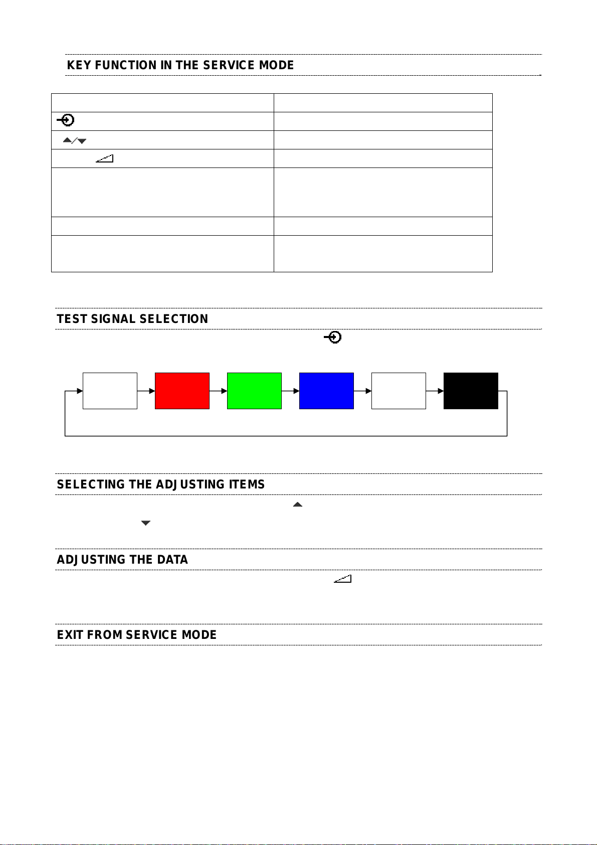
Test signal selection
(PC, Component, Composite(PAL, NTSC))
Self Check display Off
TEST SIGNAL SELECTION
1) While displaying the adjustment menu, every pressing of button on the Remote Control changes the
built-in test patterns on screen as described below.
Normal
Picture
Blue screen Green screenRed screen
Whe
n a pattern is changed at the time of an ATV display, it can display only for a moment.
SELECTING THE ADJUSTING ITEMS
1) While displaying the adjustment menu, press the P button to cycle through the adjustment items in the
order of table. (P
button for reverse order)
ADJUSTING THE DATA
1) While displaying the adjustment menu, press the VOLUME +/– button to change the value of data in
the range from 00H to FFH. The variable range depends on the adjusting item.
EXIT FROM SERVICE MODE
1) Press the [Exit] button on Remote.
ADJUSTING ITEMS IN THE SERVICE MODE
Item Description
RCUT RED CUTOFF
GCUT GREEN CUTOFF
BCUT BLUE CUTOFF
RDRV RED DRIVE
GDRV GREEN DRIVE
BDRV BLUE DRIVE
OSRC COOL R-CUTOFF-OFFSET for COOL
OSRC NATURAL R-CUTOFF-OFFSET for NATURAL
OSRC WARM R-CUTOFF-OFFSET for WARM
OSGC COOL G-CUTOFF- OFFSET for COOL
OSGC NATURAL G-CUTOFF -OFFSET for NATURAL
OSGC WARM G-CUTOFF-OFFSET for WARM
(3/3)
OSBC COOL B-CUTOFF-OFFSET for COOL
OSBC NATURAL B-CUTOFF-OFFSET for NATURAL
OSBC WARM B-CUTOFF-OFFSET for WARM
OSRD COOL R-DRIVE-OFFSET for COOL
OSRD NATURAL R-DRIVE-OFFSET for NATURAL
OSRD WARM R-DRIVE-OFFSET for WARM
OSGD COOL G-DRIVE-OFFSET for COOL
OSGD NATURAL G-DRIVE-OFFSET for NATURAL
OSGD WARM G-DRIVE-OFFSET for WARM
OSBD COOL B-DRIVE-OFFSET for COOL
OSBD NATURAL B-DRIVE-OFFSET for NATURAL
OSBD WARM B-DRIVE-OFFSET for WARM
OSRD 3D COOL R-DRIVE-OFFSET for COOL (3D)
OSRD 3D NATURAL R-DRIVE-OFFSET for NATURAL (3D)
OSRD 3D WARM R-DRIVE-OFFSET for WARM (3D)
OSGD 3D COOL G-DRIVE-OFFSET for COOL (3 D)
OSGD 3D NATURAL G-DRIVE-OFFSET for NATURAL (3D)
OSGD 3D WARM G-DRIVE-OF FSET for WARM (3D)
OSBD 3D COOL B-DRIVE-OFFSET for COOL (3D)
OSBD 3D NATURAL B-DRIVE-OFFSET for NATURAL (3D)
OSBD 3D WARM B-DRIVE-OFFSET for WARM (3D)
LED INDICATIONS FOR SERVICE
SW Upgrade and Error conditions indicated by the Power LED is described below.
Power LED
/
Green blink SW Upgrade in Progress
Red SW Upgrade Failed
Green SW Upgrade Successful
HOTEL MODE
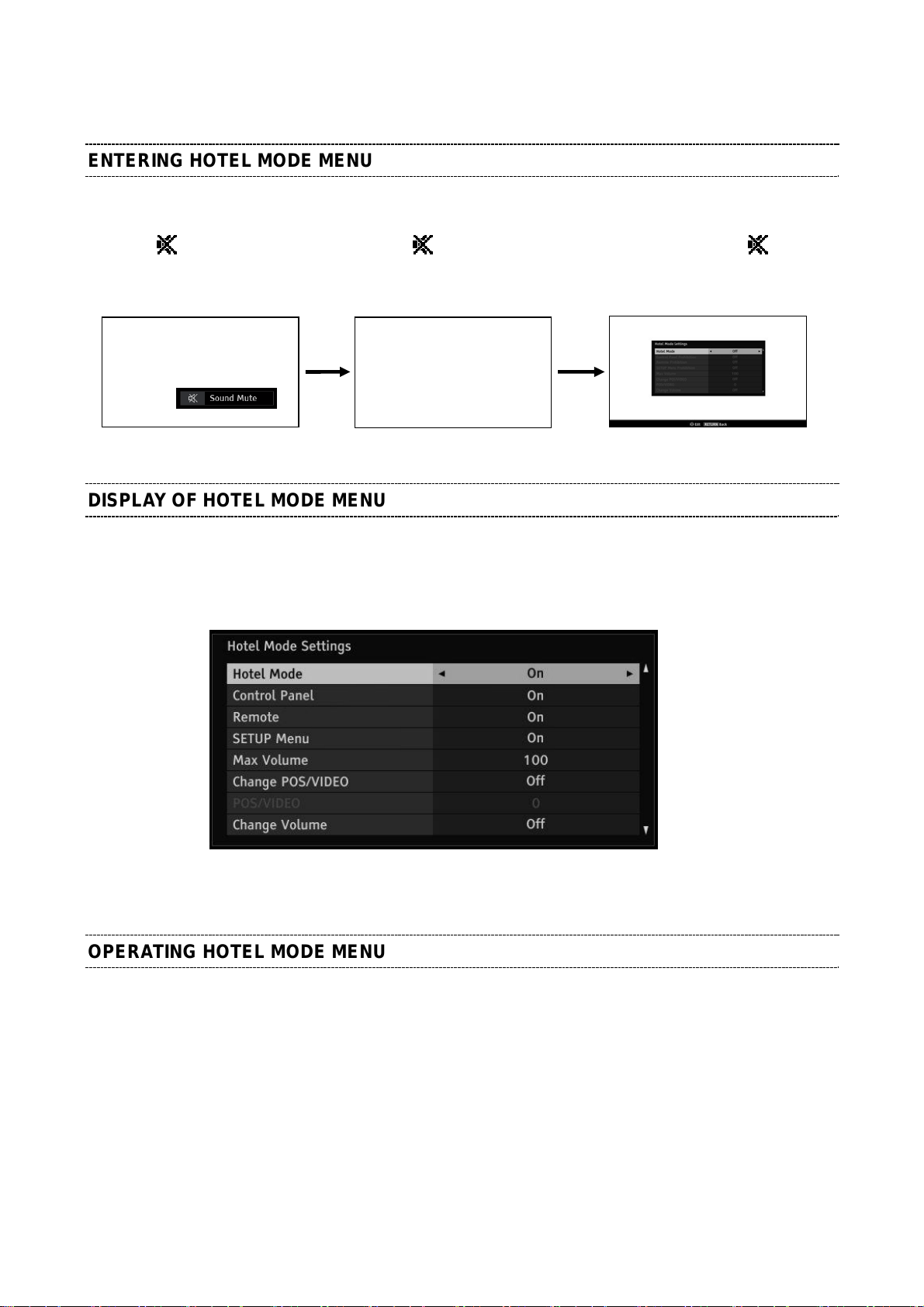
ENTERING HOTEL MODE MENU
Hotel Mode Menu should be shown by the following operation.
1) Press any button on TV to activate Touch Sensor. White LED will light up.
(1/6)
2) Press
Remote Control. keep pressing. press “+” button on TV.
button once on the 3) Press button again and 4) While pressing the button,
(Hotel Mode Settings Menu)
DISPLAY OF HOTEL MODE MENU
- The Graphic Design and color of Hotel Mode Menu is the same as the User menu.
(Small differences which do not affect to operation will be acceptable)
- The language will follow the “Menu Language” setting in the menu
(Example of Menu Image)
OPERATING HOTEL MODE MENU
- To enable Hotel Mode, use the or arrow keys while “Hotel Mode” item is highlighted to select “On”.
Once Hotel Mode is on, the Hotel Mode settings will be enabled for adjusting.
- Use ▲ and ▼ buttons to access the hotel mode settings.
Use and buttons to change the settings.
See the table below for explanation of each setting.
- Press Exit when finished adjusting the settings.
(2/6)
Item Options Description
Hotel Mode
Control Panel
Off Disable Hotel Mode.
All the settings of Hotel Mode
are disabled.
On Enable Hotel Mode
On Allow use of all Control panel
buttons
Off Prohibit use of all control panel
buttons.
But, Power Off -> On by control
panel POWER button is not
prohibited.
(Power On -> Off is prohibited.)
* Entering Service mode/Hotel
mode Menu/Hotel Clone is not
Off -
On - Grayed out when "Hotel
Factory
Gray Out Conditions
settings
Mode" = [Off]
prohibited.
* Control panel buttons are
available during Service mode.
(3/6)
Setup Menu
On Remote Enabled Remote Control
Off Remote Disabled
* The following remote codes are
not disabled.
- SOUND MUTE (40BF10)
- Super User mode (40BFFE)
- S mode (40EEC3)
* Remote Enabled during Service
mode/Hotel mode Menu/Hotel
Clone.
* When Remote Control is set to
“Off”, the [Panel Lock] setting in
the main menu will be grayed out
and forced to “Off”.
On Allow access to SETUP menu
Off Prohibit access to the setup
On - Grayed out when "Hotel
Mode" = [Off]
On - Grayed out when "Hotel
Mode" = [Off]
menu.
SETUP menu icon is grayed out
and it is prohibited to select
(skip).
(If gray-out of SETUP menu icon
is difficult,
skipping without gray-out is
acceptable )
Off (Except
Language)
Max Volume 0-100 Set maximum volume level.
Prohibit access to all items in the
setup menu except for the
Language setting.
The prohibited items are not
shown on the menu. (Gray-out
instead of erasing is acceptable)
It limits the volume level which
100 - Grayed out when "Hotel
Mode" = [Off]
can be set by Volume button.
If you set it to 70, Volume bar can
not go to 71 or higher.
(4/6)
Change POS/VIDEO
POS/VIDEO
(only available when
“Change POS/VIDEO”
is On)
Off TV Tunes to the last channel or
input viewed when powered on
On TV tunes to preset
“POS/VIDEO” (channel or input)
when TV is powered on.
On (AC) TV tunes to preset
“POS/VIDEO” (channel or input)
only when AC power is applied.
When TV is powered on by
power button, tune to the last
channel or input.
0-99 0-99 (ATV Channel Position)
DTV DTV (DTV channel number can
not be set. The last selected
channel is shown.)
Off - Grayed out when "Hotel
Mode" = [Off]
0
- Grayed out when Hotel
Mode = [Off]
- Grayed out when
"Change POS/VIDEO" =
Change Volume
Volume
(only available when
VIDEO1 VIDEO1
VIDEO2 VIDEO2
VIDEO3 VIDEO3
HDMI1 HDMI1
HDMI2 HDMI2
HDMI3 HDMI3
HDMI4 HDMI4
PC PC
Off TV volume level does not
change when TV powers on
On TV volume level is forced to
“Volume” level when TV is
powered on
0-100 Volume level when TV is
powered on
* The input which
does not exist on
the model should
not be shown.
(eg. “DTV” is not
shown on ATV
models.)
[Off]
Off - Grayed out when "Hotel
Mode" = [Off]
30
- Grayed out when "Hotel
Mode" = [Off]
“Change Volume” is
On)
- Grayed out when
"Change Volume" = [Off]

(5/6)
Change Picture Mode
Picture Mode
(only available when
“Change Picture Mode”
is On)
Off Picture setting mode does
not change when TV is
powered on
On Picture setting mode is
forced to “Picture Mode”
mode when TV is powered
on
AutoView AutoView
Dynamic Dynamic
Standard Standard
Movie 1
(EU: Hollywood
Day)
Movie 2
(EU: Hollywood
Night)
Movie 1
(EU: Hollywood Day)
Movie 2
(EU: Hollywood Night)
Off - Grayed out when "Hotel
Mode" = [Off]
AutoView - Grayed out when "Hotel
Mode" = [Off]
- Grayed out when
"Change Selectable
Picture" = [Off]
TV Power
Position Change on
HDMI Input
Disabled TV returns to previous
Standby/On State when
AC power is applied
Force On Power TV on when AC
power is applied
Force Standby Put TV in Standby when
AC power is applied
On
Off When viewing HDMI input,
RF tuning via P
RETURN, and number
buttons is allowed.
(Normal operation)
RF tuning via P▲, P▼,
RETURN, and number
buttons is disabled
▲, P▼,
Disabled - Grayed out when "Hotel
Mode" = [Off]
On - Grayed out when "Hotel
Mode" = [Off]
(6/6)
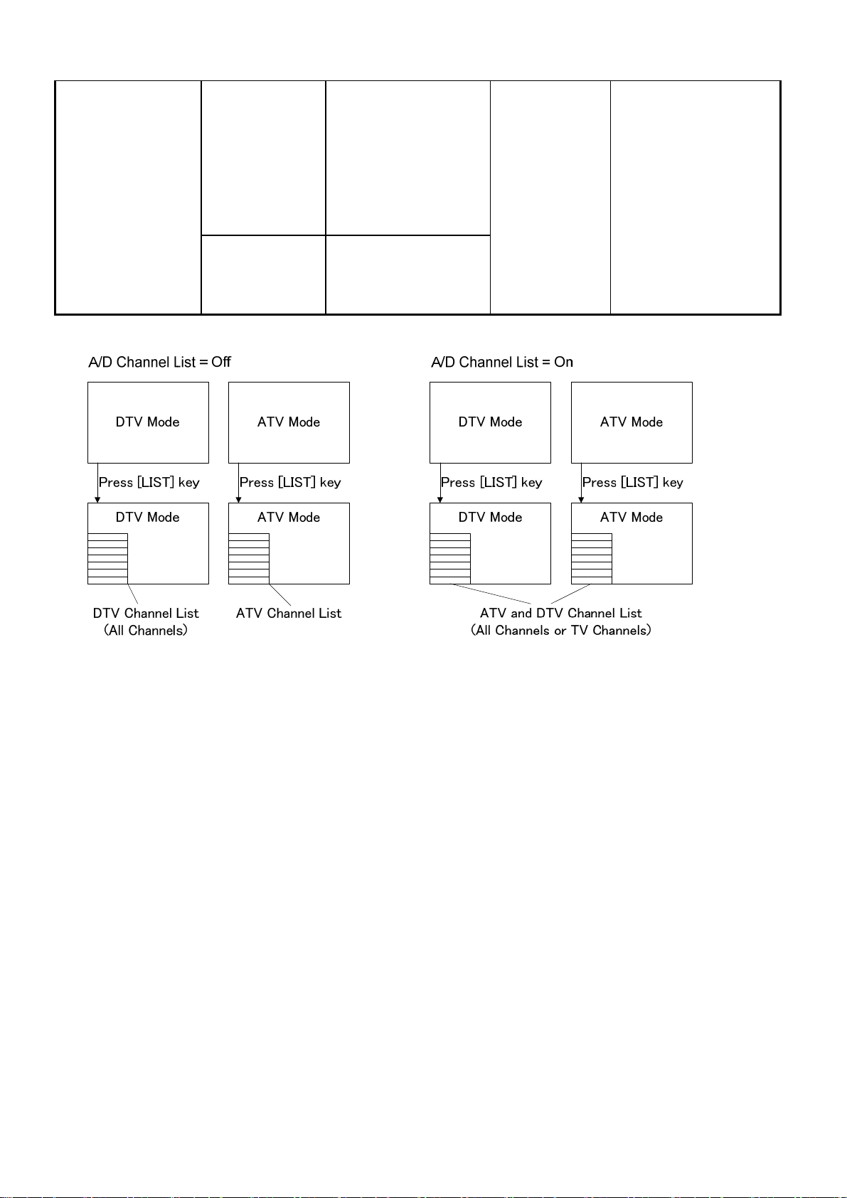
A/D Channel List
On TV shall combine both
Analogue & Digital
channels in one channel
list, and select the
ATV/DTV channel without
boarder.
Off DTV Channel List and
ATV DTV Channel List are
separated.
Off - Grayed out when "Hotel
Mode" = [Off]
HOTEL CLONE
The following settings can be copied between sets using the Hotel clone menu:
● Hotel mode menu settings
● DTV Channel Setup (DTV models only)
● ATV Channel Setup
▪ Programme (position)
▪ System
▪ Colour System
▪ Programme Skip
▪ Channel
▪ Manual Fine Tuning
▪ Label
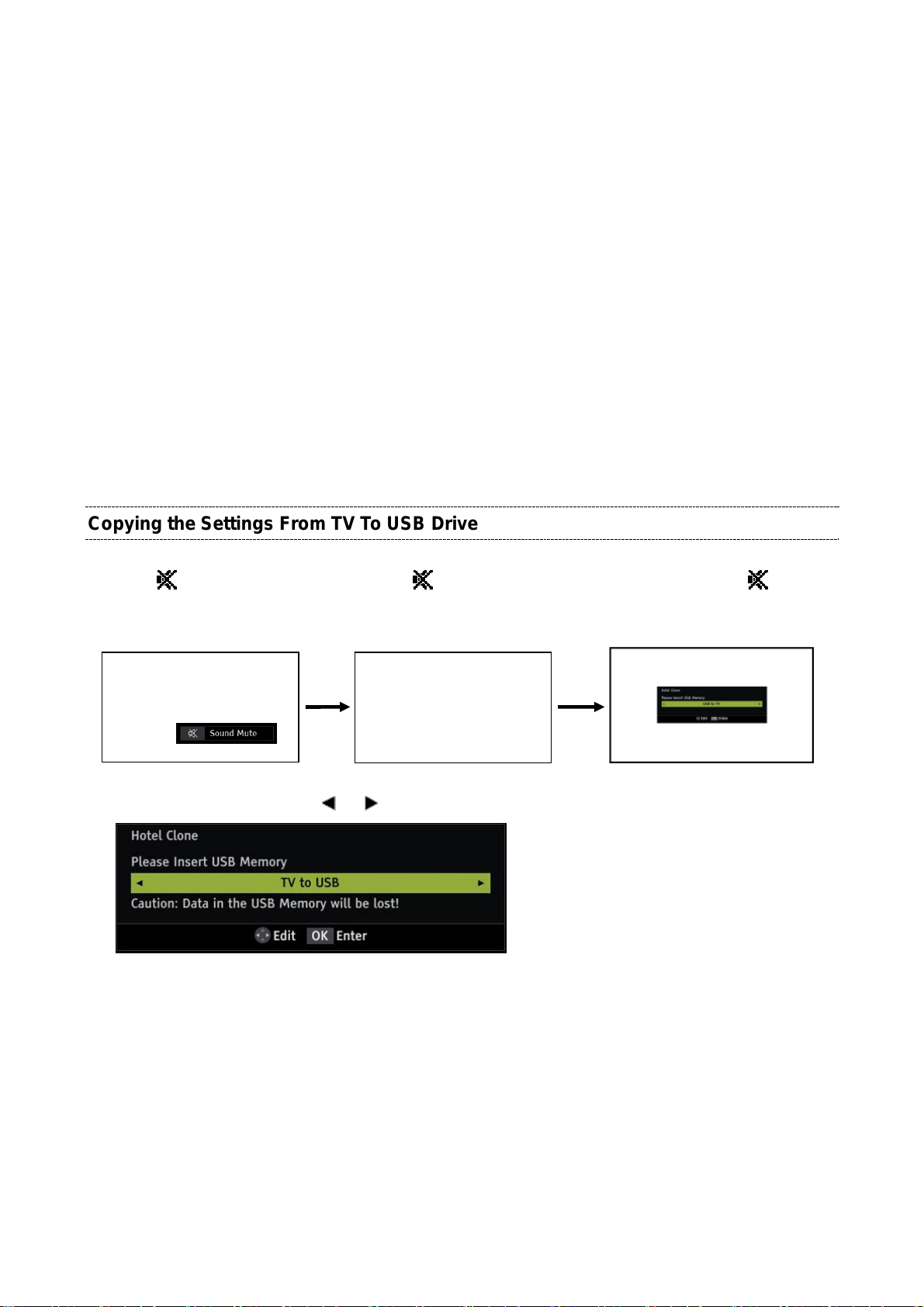
Copying the Settings From TV To USB Drive
(1/2)
1) Press
Remote Control. keep pressing. press “-” button on TV.
4) Select "TV to USB" using the
5) Insert USB Drive and press OK to copy settings to the USB drive.
6) Wait for window that indicates the copying process is complete before removing the USB drive.
button once on the 2) Press button again and 3) While pressing the button,
(Hotel Clone menu display)
or arrow keys.

Copying the Settings from USB Drive to TV
(2/2)
1) Press
button once on the 2) Press button again and 3) While pressing the button,
Remote Control. keep pressing. press “-” button on TV.
4) Select "USB to TV" using the or arrow keys.
5) Insert USB Drive that settings have previously been saved to and press OK to copy settings to the TV.
6) Wait for settings to be copied.
When the copying has finished successfully, the message "The TV will reboot when this window is
(Hotel Clone menu display)
closed." will be displayed. If the copying is not successful, an error message will be displayed.
7) Exit the menu and the TV will reboot.
8) Remove the USB drive.
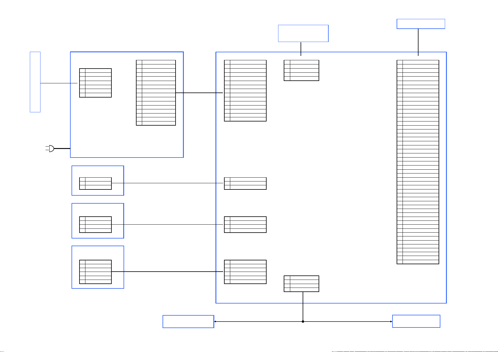
PANEL (LED B/L)
E320
E280
E260
E270 IR BORAD
PANEL (T-CON)
E290
WLAN MODULE
E350
CON201 CN90 CN162 CN650
CON301 2 12.5V 2 12V 2 GND 2 VCC_LCD
1 Anode1 3 12.5V 3 12V 3 M_USB1DP 3 VCC_LCD
2 Anode2 4 GND_12.5V 4 GND 4 M_USB1DM 4 VCC_LCD
3 Anode3 5 GND_12.5V 5 GND 5 5V_WLAN 5 NC
4 NC 6 12.5V_Audio 6 12V_AUDIO 6 GND
5 Cathode1 7 GND_Audio 7 GND_AUDIO 7 GND
6 Cathode2 8 GND_12.5V 8 (NC) 8 GND
7 Cathode3 9 GND_12.5V 9 GND 9 GND
E250
POWER BOARD
1 12.5V 1 12V 1 GND 1 VCC_LCD
E344
10 5V 10 5V1 10 GND
11 GND_5V 11 AC_DETECT 11 LVB4P
12 ACD 12 POWER_TV 12 LVB4N
13 PS_ON 13 BL On/Off 13 LVB3P
14 BL_ON 14 PWM2 14 LVB3N
15 NC 15 PWM1 15 GND_T1
16 PWM1 16 LVBCKP
E200
MAIN BOARD
KEY BORAD
1 GND 1 GND 30 LVA3N
2 ADC_IN 2 Func Key 31 GND_T1
3 POWER_KEY 3 Power Key 32 LVACKP
E348
CN743 29 LVA3P
LED BORAD
1 LED_5V1 1 RED 40 LVA0N
2 GND 2 GREEN 41 GND
3 GREEN 3 GND 42 NC/NC/LD-Ena
4 RED 4 5V1 43 NC/TMPS1/NC
1 3.3VD_IR 1 3.3VD 51 NC/NC/3D-En
2 GND 2 GND
3 Br Sensor 3 Br Sensor
4 GND 4 GND CN300
5 3.3V_STNBY_IR 5 3.3V_STNBY 1 R-SPK
6 RMT_IN 6 RMT_IN 2 R+SPK
E346
E342
CN742 39 LVA0P
CN741 50 NC/NC/NC
3 L-SPK
4 L+SPK
E310A
(For AUO Panel)
75034227 (RA)
75034228 (RB)
17 LVBCKN
18 GND_T1
19 LVB2P
20 LVB2N
21 LVB1P
22 LVB1N
23 LVB0P
24 LVB0N
25 NC/LR_SW/NC
26 NC/3D_EN/NC
27 LVA4P
28 LVA4N
33 LVACKN
34 GND_T1
35 LVA2P
36 LVA2N
37 LVA1P
38 LVA1N
44 NC/TMPS0/NC
45 LVDS_SEL(L)
46 NC/NC/NC (PWM)
47 NC/NC/I2CCK
48 NC/NC/I2CDA
49 NC
E310B
(For SAM Panel)
75034462 (RA)
75034463 (RB)
Speaker
E340
Speaker
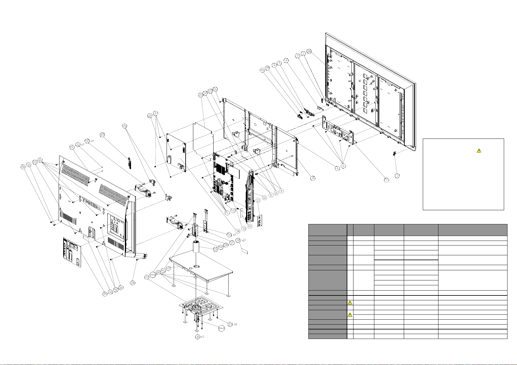
EXPLODED VIEW
)
t
e
y
32L4363D
SAFETY PRECAUTION
The parts identified by mark
are critical for safety. Replace only
with part number specified. Th
mounting position of replacement
is to be identical with originals.
The substitute replacement parts
which do not have the same safet
characteristics as specified in the
parts list may create shock, fire or
other hazards.
32L4363D(G)/(N
No. Location
1
4
5
12+13
17+18+19+(24-1)
22+20+29+31
23+25+26+27+30
35
36
37
38
39
40
42
43
Toshiba
Service Par
E104 75033745 13EB-45Q0601 FILTER
E102 75033744 13EB-45Q0101 LED LENS
E106
E140
E150 75034221 13EB-44B0701 NECK ASSY
E110
E120 75034217 9C-EB40S02F0 STAND ASSY
E200 75034461 9C-EB40M0200 MAIN BOARD ASSY
E250 75034252 0433-007Y000 POWER BOARD ASSY
E330 75034229 04A4-01CK000 SPEAKER (LEFT AND RIGHT)
E300A 75033812 LCD PANEL, AUO
E300B 75033810 LCD PANEL, SAM
E260 75034223 9C-EB40S02E0 LED BOARD ASSY
E270 75034224 9C-EB40S02D0 IR BOARD ASSY
E290 75034226 0C05-00JK0TB WLAN MODULE
E280 75034225 9C-EB40S02C0 KEYPAD BOARD ASSY
75033813 13EB-45Q0K11
75033814 13EB-45Q0411
75034219 13EB-44B0G01
75034256 13EB-44B0G11
75034457 13EB-45B0G11
75034458 13EB-45B0C11
75034459 13EB-45B0G02
75034460 13EB-45B0C02
ODM Partner
Part
Description
SUPPORT FOR SMALL BOARD
SIDE KEY BEZEL ASSY
BACK COVER ASSY
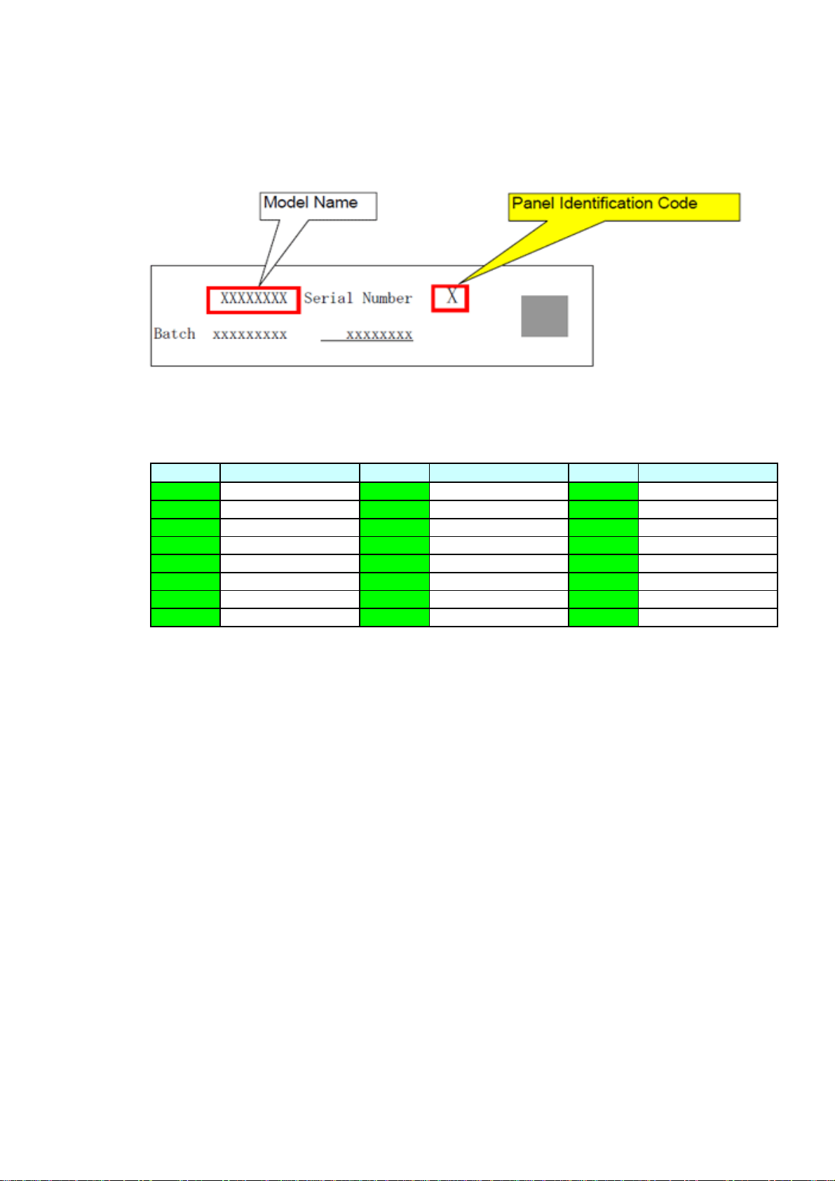
PANEL IDENTIFICATION
A
Serial No. part printed on Rating Label
Panel Identification Code
Marking Marking Marking
BKT
CLU
DMV
ENW
FPX
GQY
HRZ
Panel Vendor
AUO
BriView
CMO
CHILIN
IPS
JS
Panel Vendor
SAMSUNG
LPL/LGD
CPT
Panel Vendor
SHARP
(1/3)
MAIN BOARD EXCHANGE
When Main board is exchanged, the Application SW (Firrmware) and Model Setting need to
be updated.
Please update in the following procedures.
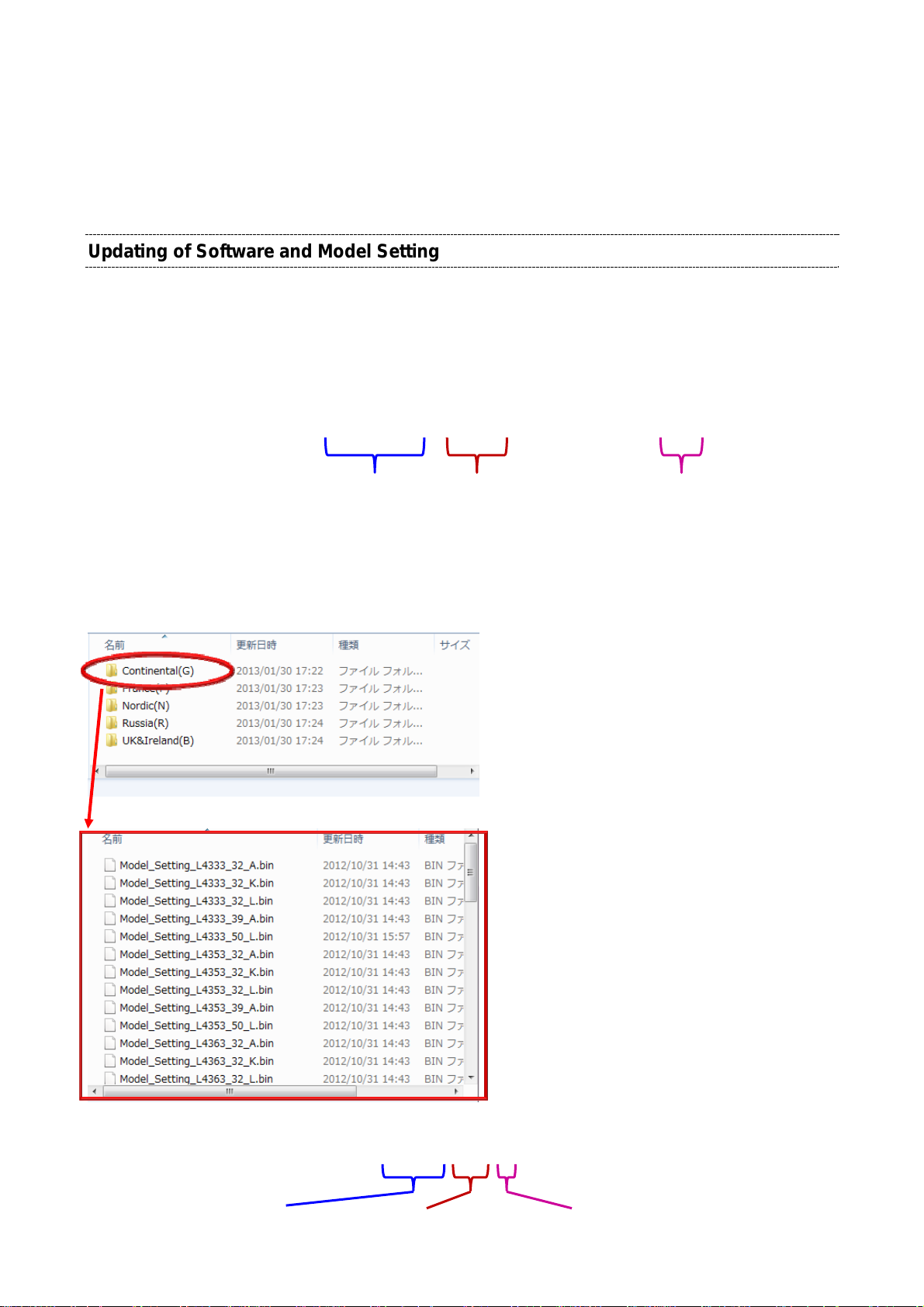
Updating of Software and Model Setting
1. Copy the Application SW (Firmware) file and the Model Setting file to the root of the USB
mass storage device.
Application SW:
[Example] UPDATE_50L7363C_12800_INIT_CLEAR#.enc
This Application SW is for not
only 50L7363C but also the other
models, i.e. all of L73/L63/L43
models.
Model Setting File:
This number is
an example.
“enc” means encrypted.
This SW is encrypted for
security.
Model settin
Each Shipout folder contains model setting files.
g files are categorized by shipout.
[Example] Model_Setting_L4333_32_A.bin
TV series
Panel size Panel Vendor
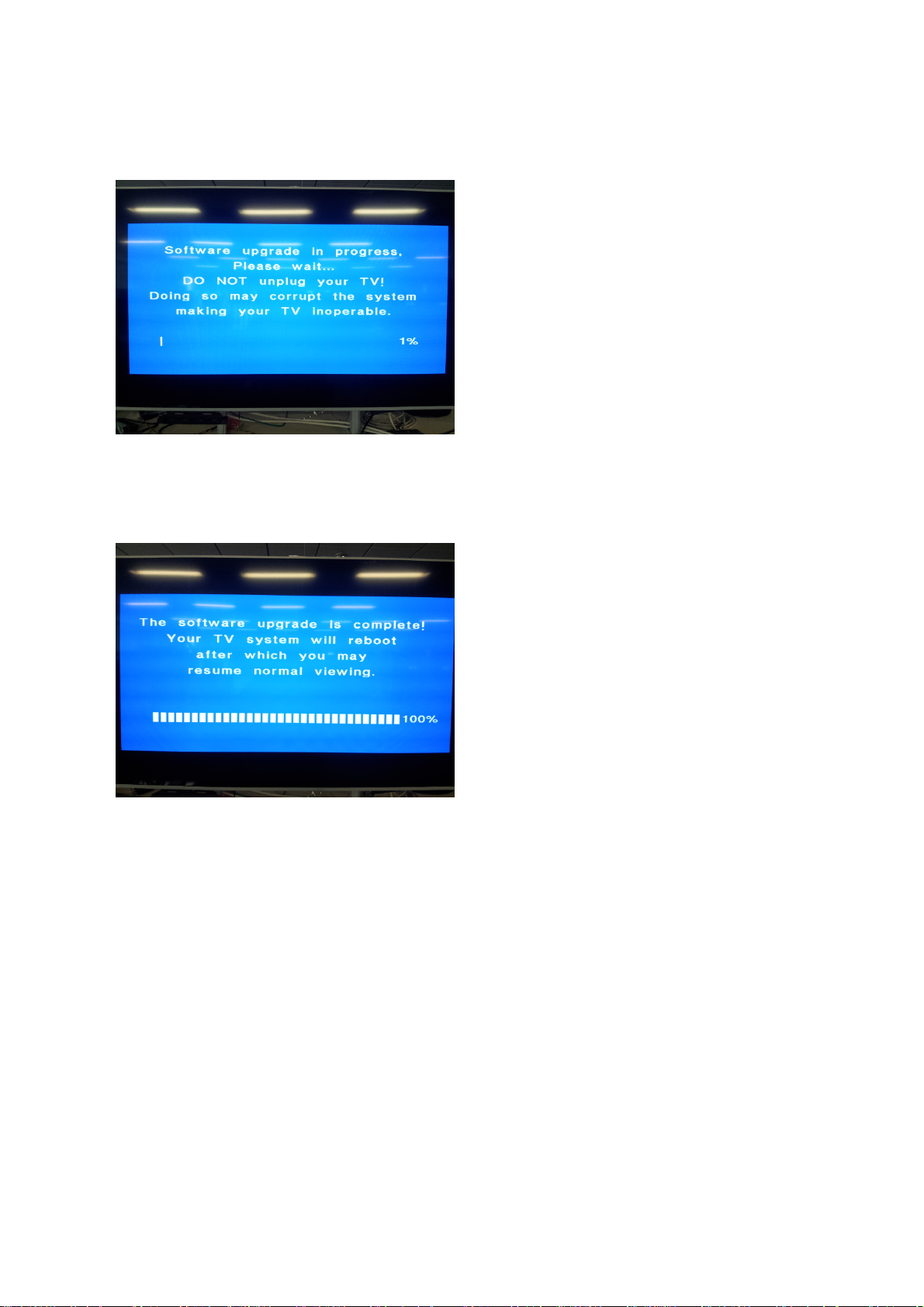
2. Unplug TV, and then Insert the USB mass storage device to the USB slot of the TV.
3. Plug TV.
Software updating starts.
If Software updating does not start and the front LED lights red, then press [Power] key on
Remote Control to start Software updating.
4. After updating complete, unplug TV and remove the USB mass storage device.
(2/3)
5.
Plug TV, then check the updating by using self check screen.
Refer to “Confirmation of Software updating” section on next page.
6. Update to the newest SW.
This model can be updated from aerial or network to the newest Software.
Refer to the user manual of this model for the updating method.
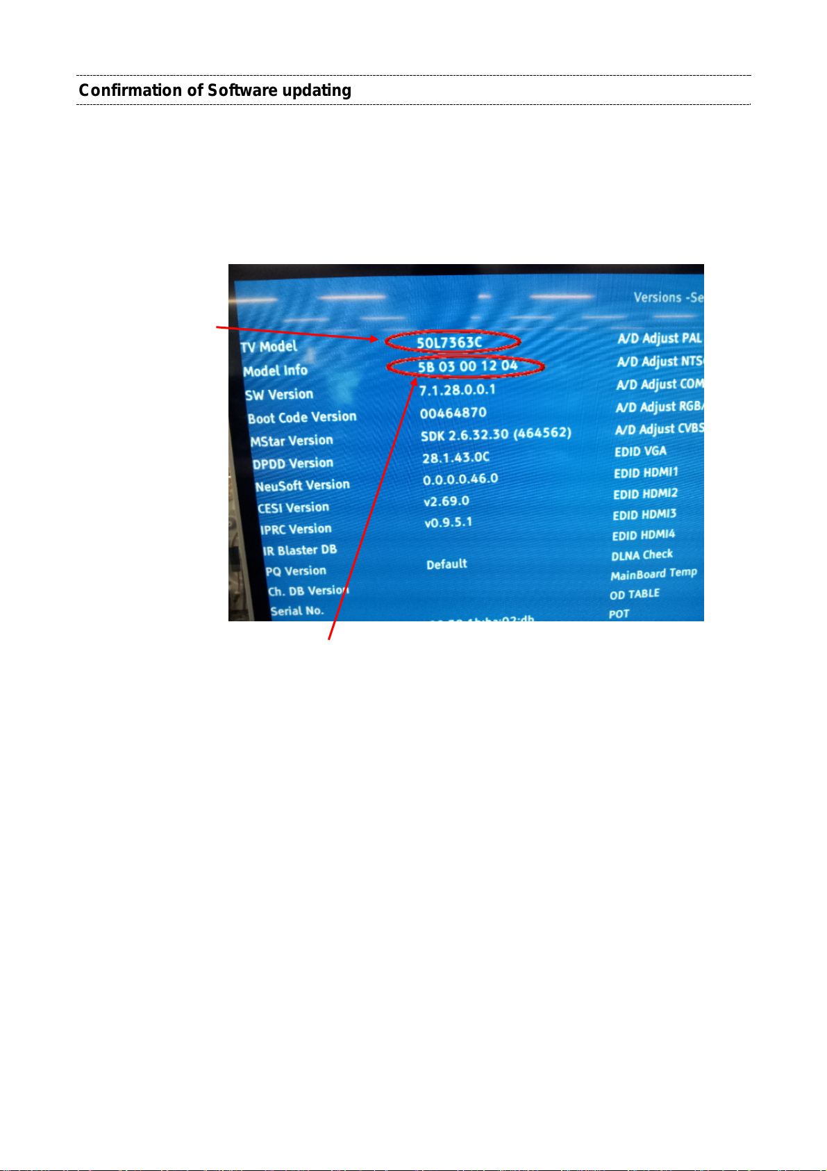
Confirmation of Software updating
Check the TV Model and Model Info by using self check screen.
1. Press SETUP on Remote Control.
2. Select “Get Help” >> “System Information”
3. Press “3” “5” “7” “4”
Self check screen is displayed.
TV model and
Panel vendor
(3/3)
th
[The 4
number and Shipout]
10 UK&Ireland (B)
11 France (F)
12 Continental(G)
13 Russia (R)
14 Nordic (N)
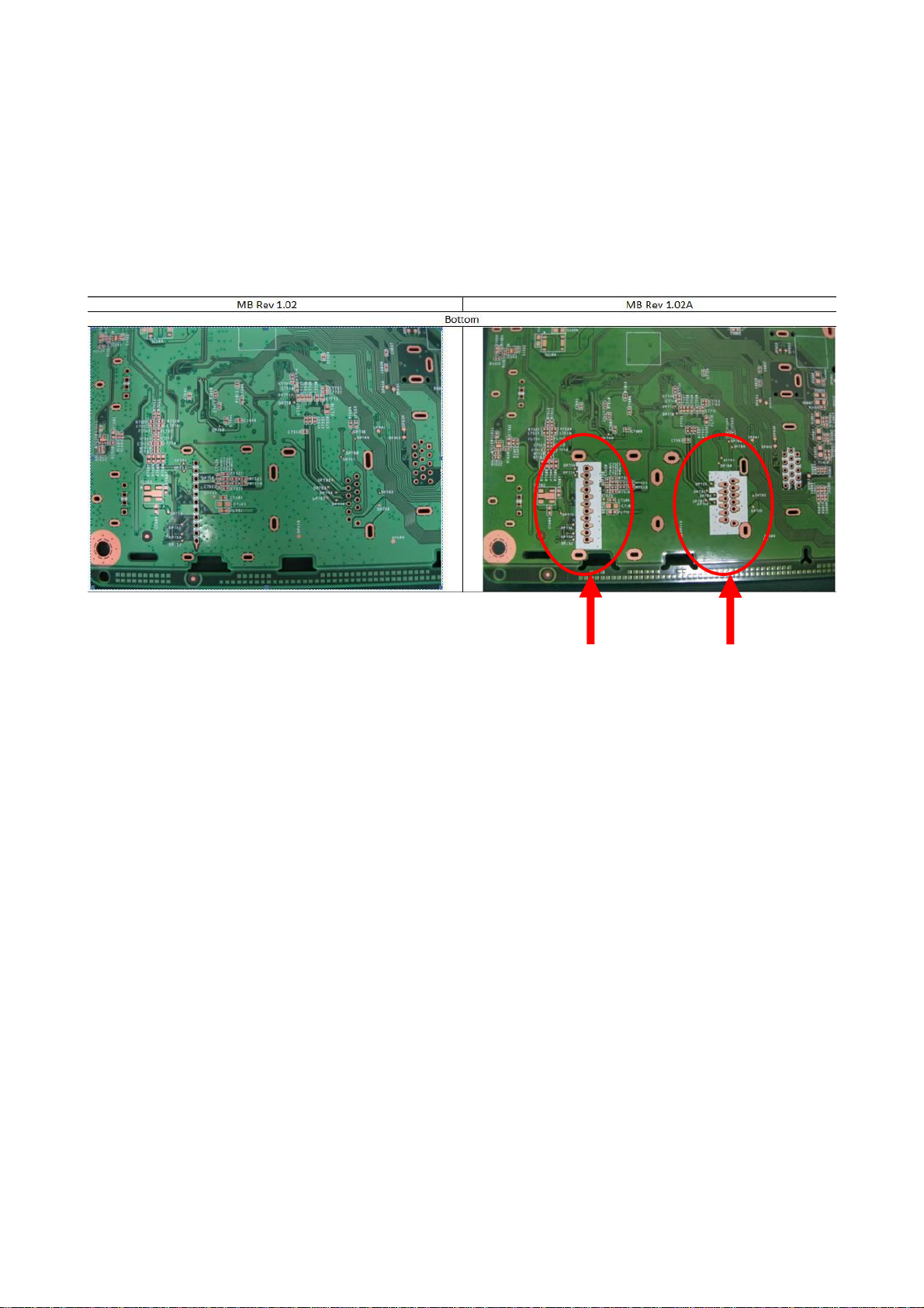
ABOUT THE MAIN BOARD
The Main PCB is changed to enable easier removal of Tuner.
The old one is 1.02, the new one is 1.02A. For Service Parts, only new type is used.
The new type (1.02A) have larger land pattern for soldering the Tuner.
And around the land, attached white silk marking.

REV. 00
May/8/2013
TOSHIBA 2013 L7363 Series Models
VerDate
Stage
SR
2012/10/04 1.01 R_SPI_CLK / R_SPI_CS swap R_SPI_CLK / R_SPI_CS net swap in IC760 side:
ER
2012/10/29
ER
Design Notes
1.002012/09/20 SR Stage Release
1.012012/10/04 1. Change IC790 pin19’s net name to S_CI_BUFFER_ENZ
Add S_CI_BUFFER_ENZ to
ctrl CI Data buffer
ER
2012/10/23 1.01 Test Point change Chage CN741,CN742,CN743,CN652,CN162,CN100 test point size for DFM review
ER
2012/10/26 1.01 Add schumitt buffer on 796 and GPIO
ER
ER
ER
2012/10/26 1.01 GPIO change from IC100 to CI BUS3
ER
ctrl
1.012012/10/26
PC EDID & debug by VGA
IC790
IC790
2012/10/29 1.01 PJ601 change 603 PJ601 was changed to 1242-00KB000ER
2012/10/29 Remove Resistances list below:
2012/10/29 1. Change: R6580 100 KOhm → 4.7KOhm
ER 1.01 Circuit Change Notes_2012/10/26:
2012/10/29 ER 1.01 Circuit Change Notes_2012/10/26:
2012/10/29 ER 1.01 Circuit Change Notes_2012/10/26:
ER2012/10/29 1.01 Circuit Change Notes_2012/10/26:
2012/10/29 ER 1.01 Circuit Change Notes_2012/10/26:
2012/10/29 ER 1.01 Circuit Change Notes_2012/10/26:
2012/10/30 R6584 optional change from NC to NC4NC5NC6NC7NC8658Circuit Change Notes 2012/10/26:
2012/10/30 950 12V & 12V_3 swap in the both side of FL957ER 1.01 Circuit Change Notes_2012/10/26:
2012/10/30 ER 1.01 791 1. Change IC789 from TPS2553DBV-1 to R5524N001B-TR-FE
2012/10/30 ER 1.01 Circuit_Notes_TUNER_Demod_2:
2012/10/31 ER 1.01 Test Point requested by production test 660 Add DP716 in net H_PWR4
2012/10/31 ER 1.01 R1218 NC 135 R1218: Mount -> Not Mount
2012/11/01 ER 1.01 Add DP721 for DFM 658 Add DP721 for DFM
ER 1.01 Add Bead for EMI 658
2012/11/01
ER 1.01 D7410 & D7411 NC 9512012/11/07 Keypad D7410 & D7411 NC
2012/11/14 ER 1.01 Change R6580 => 12k Ohm 658 Change R6580 => 12k Ohm
Circuit Change Notes_2012/10/26:
1.01ER
Remove below 0 ohm resistors for
current measure and connect directly
FET Unmount and Relevant Changes
in 3D GLASSES I/F
Insert FL909 & FL957
Place R1218 near IC100.
R6712 and R6713 are deleted
T-CON POWER SW change
Tuner component fine tune
1.01ER
correction
correction
Circuit Change Notes_2012/10/30:
Circuit_Change_Notes_CI3
SHT755 S TUNER
Description
Page
760
R_SPI_CS => IC760.33 / R_SPI_CLK => IC760.28
Res R7613 & RM761C SWAP for easy layout ( 2012/10/29 add)
113, 794
2. Connect S_CI_BUFFER_ENZ to IC100.C7 (GPIO81)
3. reserve a pull-up resistor R1002 on S_CI_BUFFER_ENZ
Tuner H7550 => 04A9-00DF0TB & H7501 => 04A9-00DB0TB2012/10/04 1.01 Tuner change
755,
750
121, 658,
700
104, 796 1. Add R_TSCLK_CI ( from R1130 to IC794.2 ) & R_TSCLK ( from R1131 to R7740 & R7742 )
2. Add Scheumitt buffer ( IC794, R7950, C7963 )
1. Delete DP100 and DP102
113, 609GPIO & related circuit change for DSUB
2. Connect IC100's GPIO5 -> VGA_EEP_WP ( -> Q6110.G, Q6025.G & Q6026.G )
GPIO16 -> M_VDBG_EN ( -> IC620.7 )
GPIO110 -> M_DSUB_I2CCLK ( -> Q6026.S )
GPIO108 -> M_DSUB_I2CDATA ( -> Q6025.S )
113, 6692012/10/26 1.01 GPIO change from IC100 to CI BUS3
1. Delete DP103.
2. Connect IC100's GPIO81 and R6637 by M_WP_HDCP
113, 794 1. Delete DP109.
2. Connect IC100's GPIO8 and R7900 by C_CI_BUS_ENZ
117, 129,
R1103, R1232, R1237, R1601, R1604, R1606, R1608, R6520, R6650, R6651,
160, 653,
R6710, R6711, R6728, R7803, R7804, R7805, R7806, R7807, R7808, R7809,
665, 674,
R7810, R7811, R7812, R7919, R7920, R9000, R9001, R9090,R9091
780, 791,
901, 906
658
2. Mount → Unmount:
Q6582, R6585, R6586, R6587, R6589, C6581
3. Add: C6582 0.1UF/16V, R6590 0 Ohm, R6591 220 Ohm
1. Change Net Name of Power of IC905, Insert FL909 (220ohm/100MHz), and connected FL909 to 12V_3
905, 950
2. Change Net Name of 12V, Insert FL957 (220 ohm/100MHz), and add net 12V_3
135 Place R1218 near IC100.
677 R6712 and R6713 are deleted and it connects directly
653 T-CON POWER SW change
750, 751 1. Change C7506, R7514, R7557, R7714
2. Add C7524, R7610, C7617, C7563, C7731
3. Delete R7513,R7515
2. Remove R7911
755 C7563 connect to R7557 & H7550
CN652: Add FL652, FL653
700
CN741: Add FL737, FL738, FL739, FL740, FL741
CN742: Add FL743, FL744, FL745, FL746
CN743: Add FL747, FL748, FL749
653Add L6541 for T-CON circuit1.01ER2012/11/01 Add L6541 for T-CON circuit
VerDate Design Notes DescriptionStage Page
2012/11/14 PR 1.02 Part change to reduce DDR 800MHz
2012/11/28 PR 1.02 Part change to improve T-COM PWR
2012/12/05 PR 1.02 CN100 NC 121 CN100 NC
2012/12/12 PR 1.02 FL664, FL665 => 0 ohm 660 FL664, FL665 were changed to 0 ohm array for MHL
2012/12/17 PR 1.02 Change part reference 674 FL619 was renamed as FL162
2012/12/18 PR 1.02 Add test point 906 DP901 was add for IC911 pin1
2012/12/24 PR 1.02 PJ601 local use footprint for DFM 603 PJ601 change local use footprint for DFM, floating issue in 1.2mm PCB
2012/12/26 PR 1.02 ON/OFF function of the WLAN power 160 R1608 : 0 Ω -> NC
Emisson
sequence
EMI solution 600 Page 600: Add C6015, C6016, C6017, FL616~FL618
MHL VBUS / IC673 circuit change Remove R6740 & Add R6735, Q6710 near IC673674
The dischage res for T-CON PWR 653 Add R6546
1.02PR2013/01/02 700LED luminosity is adjustted R7032 : 100 -> 680Ω
improve X-tal accuracy for DVB-T2
1.022013/01/08 PR 760
& DVB-S2/S
658, 700 FL652, FL653: P/N: 0901-0019000 GBK160808T-300Y-N
FL737-FL741: P/N: 0901-0027000 GBK160808T-121Y-S<G>
FL743-FL746: P/N: 0901-0027000 GBK160808T-121Y-S<G>
FL747-FL749: P/N: 0901-0027000 GBK160808T-121Y-S<G>
653 C6543 was changed from 0.22uF to 1UF/25V (0603)
Page 602: Add C6032~C6039, FL610~FL612
Page 603: Add C6090~C6093, FL613~FL615
160 FL619 was added for wifi
Remove IC620 and C6085 & Add Q6027 & Q6028To improve the leak current from I2C 609
Add R1608, R1609, R1610USB connector for WLAN 160
R1609 : NC -> 0 Ω
R1610 : NC -> 4.7K Ω
C7614,C7615 27p -> 10p
R7606 0 ohm -> 1.8Kohm
770
C7714,C7715 6p -> 10p
R7710 0 ohm -> 1.5Kohm
improve IFAGC voltage of SoC 751 R7522 : 10Kohm -> 0ohm
Optional Information
000. History & Description
000. History & Description
000. History & Description
Title :
Title :
Title :
Engineer:
Engineer:
Engineer:
CVP DM HW
CVP DM HW
MAIN BOARD
MAIN BOARD
MAIN BOARD
Size Project Name
Size Project Name
Size Project Name
A2
EU Lv.2
A2
EU Lv.2
A2
EU Lv.2
Date: Sheet of
Date: Sheet of
Date: Sheet of
CVP DM HW
001 76Tuesday, January 08, 2013
001 76Tuesday, January 08, 2013
001 76Tuesday, January 08, 2013
Rev
Rev
Rev
1.00
1.00
1.00
101. MSD8881CV(Video)
M_ADCIMM_ADCIM
751
M_ADCIPM_ADCIP
751
M_HSYNC0M_HSYNC0
608
M_VSYNC0M_VSYNC0
608
M_BIN0MM_BIN0M
606
M_BIN0PM_BIN0P
608
VGAE1(SCART/Comp)E2(Comp)
606
608
608
606
608
600
600
606
608
606
608
606
606
608
606
606
606
606
606
606
606
M_GIN0MM_GIN0M
M_GIN0PM_GIN0P
M_SOGIN0M_SOGIN0
M_RIN0MM_RIN0M
M_RIN0PM_RIN0P
M_HSYNC1M_HSYNC1
M_VSYNC1M_VSYNC1
M_BIN1MM_BIN1M
M_BIN1PM_BIN1P
M_GIN1MM_GIN1M
M_GIN1PM_GIN1P
M_SOGIN1M_SOGIN1
M_RIN1MM_RIN1M
M_RIN1PM_RIN1P
M_BIN2MM_BIN2M
M_BIN2PM_BIN2P
M_GIN2MM_GIN2M
M_GIN2PM_GIN2P
M_SOGIN2M_SOGIN2
M_RIN2MM_RIN2M
M_RIN2PM_RIN2P
IC100B
IC100B
[V-U8881CVF]
[V-U8881CVF]
2/16
2/16
IC100A
IC100A
[V-U8881CVF]
[V-U8881CVF]
1/16
1/16
[ANALOG VIDEO INTERFACE]
[ANALOG VIDEO INTERFACE]
SIG15368
AH8
IM
AG8
AB5
AB4
W3
W2
AA3
AC6
AA2
AA1
AC3
AB2
AB3
AC1
AC2
T2
T3
U1
U2
U3
V1
V3
Y4
Y6
V2
Y2
Y3
Y1
IM
IP
IP
HSYNC0
HSYNC0
VSYNC0
VSYNC0
BIN0M
BIN0M
BIN0P
BIN0P
GIN0M
GIN0M
GIN0P
GIN0P
SOGIN0
SOGIN0
RIN0M
RIN0M
RIN0P
RIN0P
HSYNC1
HSYNC1
VSYNC1
VSYNC1
BIN1M
BIN1M
BIN1P
BIN1P
GIN1M
GIN1M
GIN1P
GIN1P
SOGIN1
SOGIN1
RIN1M
RIN1M
RIN1P
RIN1P
HSYNC2
HSYNC2
BIN2M
BIN2M
BIN2P
BIN2P
GIN2M
GIN2M
GIN2P
GIN2P
SOGIN2
SOGIN2
RIN2M
RIN2M
RIN2P
RIN2P
MSD8881CV
MSD8881CV
MSTAR/MSD8881CV-W9N
MSTAR/MSD8881CV-W9N
MOUNTING HOLES
SIG15367
SIG14412
SIG14411
SIG14413
SIG14410
SIG14403
SIG14407
SIG14408
SIG14414
SIG14409
SIG14406
SIG14405
SIG14415
SIG14404
H1
H1
1
GND9
2
GND1
3
GND2
4
GND3
C394D138
C394D138
H5
H5
1
GND9
2
GND1
3
GND2
4
GND3
C394D138
C394D138
E1(SCART/Comp)
E2(Comp)
SIG17944
H8
H8
2
112
BRACKET_2P
BRACKET_2P
GND
GND8
GND7
GND6
GND5
GND4
GND8
GND7
GND6
GND5
GND4
9
8
7
6
5
9
8
7
6
5
606
606
607
607
606
M_CVBS3M_CVBS3
M_CVBS2M_CVBS2
M_CVBS1M_CVBS1
M_CVBS0M_CVBS0
M_VCOMM_VCOM
H2
H2
1
GND9
2
GND1
3
GND2
4
GND3
C394D138
C394D138
GND8
GND7
GND6
GND5
GND4
GND_PGA
9
8
7
6
5
W6
CVBS3
SIG17950
SIG17952
SIG17946
CVBS3
W4
CVBS2
CVBS2
U5
CVBS1
CVBS1
V6
CVBS0
CVBS0
V5
VCOM
VCOM
AH6
VIFM
VIFM
AG6
VIFP
VIFP
AB11
AVSS_PGA
AVSS_PGA
MSD8881CV
MSD8881CV
MSTAR/MSD8881CV-W9N
MSTAR/MSD8881CV-W9N
1
2
3
4
GND GNDGND
H6
H6
1
GND9
2
GND1
3
GND2
4
GND3
C394DO181X157
C394DO181X157
Hole in Left down coner Hole in Right down coner
GND GNDGND
GND8
GND7
GND6
GND5
GND4
9
8
7
6
5
1
2
3
4
H3
H3
C394D138
C394D138
H7
H7
C394D157
C394D157
[ANALOG VIDEO INTERFACE]
[ANALOG VIDEO INTERFACE]
GND9
GND8
GND1
GND7
GND2
GND6
GND3
GND5
GND4
GND9
GND8
GND1
GND7
GND2
GND6
GND3
GND5
GND4
[VIF INTERFACE]
[VIF INTERFACE]
9
8
7
6
5
9
8
7
6
5
RFAGC
RFAGC
IFAGC
IFAGC
GND8
GND7
GND6
GND5
GND4
U4
W5
AG5
AF5
M_CVBSOUT1M_CVBSOUT1
R_IFAGC_SoCR_IFAGC_SoC
9
8
7
6
5
CVBSOUT2
CVBSOUT2
CVBSOUT1
CVBSOUT1
H4
H4
1
GND9
2
GND1
3
GND2
4
GND3
C394D138
C394D138
GND
101. MSD8881CV(Video)
101. MSD8881CV(Video)
Title :
Title :
Title :
Engineer:
Engineer:
MAIN BOARD
MAIN BOARD
MAIN BOARD
Size Proje ct Name
Size Proje ct Name
Size Proje ct Name
Custom
Custom
Custom
Date: Sheet of
Date: Sheet of
Date: Sheet of
EU Lv.2
EU Lv.2
EU Lv.2
Engineer:
101. MSD8881CV(Video)
CVP DM HW
CVP DM HW
CVP DM HW
101 76Tuesday, January 29, 2013
101 76Tuesday, January 29, 2013
101 76Tuesday, January 29, 2013
SCART
605
751
Rev
Rev
Rev
1.00
1.00
1.00
 Loading...