

toshiba 29VH27E DIAGRAMS

050-200332
TOSHIBA
SERVICE MANUAL
COLOUR TELEVISION
29VH27E
AK52 Chassis
PRINTED IN UK. 2003 C

SM52-DRX_IF

TABLE OF CONTENTS
1.INTRODUCTION.......................................................................................................................... 1
2.TUNER........................................................................................................................................ 1
3.IF PART (DRX 3960A)................................................................................................................. 1
4.VIDEO SWITCH TEA6415............................................................................................................ 2
5.MULTI STANDARD SOUND PROCESSOR ..................................................................................2
6.SOUND OUTPUT STAGE WITH TDA7480L ................................................................................. 2
7.VERTICAL OUTPUT STAGE WITH TDA8177F............................................................................. 2
8.VIDEO OUTPUT AMPLIFIER TDA6109........................................................................................ 2
9.POWER SUPPLY (SMPS)............................................................................................................ 3
10.MICROCONTROLLER SDA5550................................................................................................ 3
10.1.General Features................................................................................................................ 3
10.2.External Crystal and Programmable Clock Speed.............................................................. 3
10.3.Microcontroller Features.................................................................................................... 3
10.4.Memory .............................................................................................................................. 3
10.5.Display Features................................................................................................................. 3
10.6.ROM Characters................................................................................................................. 3
10.7.Acquisition Features.......................................................................................................... 4
10.8.Ports................................................................................................................................... 4
11.SERIAL ACCESS 32K EEPROM................................................................................................ 4
12.CLASS AB STEREO HEADPHONE DRIVER TDA1308............................................................... 4
13.SAW FILTERS........................................................................................................................... 4
14.IC DESCRIPTIONS .................................................................................................................... 4
14.1.TDA6109............................................................................................................................. 5
14.1.1.General Description ..................................................................................................... 5
14.1.2.Features....................................................................................................................... 5
14.1.3.Pinning......................................................................................................................... 5
14.2.27W401............................................................................................................................... 5
14.2.1.Description................................................................................................................... 5
14.2.2.Features....................................................................................................................... 5
14.2.3.Connections................................................................................................................. 6
14.3.24LC32A............................................................................................................................. 6
14.3.1.Description................................................................................................................... 6
14.3.2.Features....................................................................................................................... 6
14.3.3.Pin Descriptions........................................................................................................... 7
14.4.SDA5275............................................................................................................................. 7
14.4.1.Features....................................................................................................................... 7
14.4.2.Pin Definition and functions......................................................................................... 8
14.5.DRAM 4MX4........................................................................................................................ 9
14.5.1.General Description ..................................................................................................... 9
14.5.2.Features....................................................................................................................... 9
14.5.3.Pin Assignment............................................................................................................ 9
14.6.SDA9400............................................................................................................................10
14.6.1.General Description ....................................................................................................10
14.6.2.Features......................................................................................................................10
14.6.3.Pin Definition ..............................................................................................................11
14.7.LM317T..............................................................................................................................11
14.7.1.Description..................................................................................................................11
14.7.2.Features......................................................................................................................11
14.8.DDP3310............................................................................................................................12
14.8.1.Description..................................................................................................................12
14.8.2.Features......................................................................................................................12
14.8.3.Pin connection and short descriptions.......................................................................12
14.9.SDA5550............................................................................................................................14
14.9.1.General definition........................................................................................................14
14.9.2.Features......................................................................................................................14
14.10.TEA6415C........................................................................................................................15
14.10.1.General Description ..................................................................................................15
14.10.2.Features....................................................................................................................15
14.10.3.Pinning......................................................................................................................16
i

14.11.VPC3230D........................................................................................................................16
14.11.1.General Description ..................................................................................................16
14.11.2.Pin Connections and Short Descriptions..................................................................16
14.12.TDA1308T ........................................................................................................................18
14.12.1.General Description ..................................................................................................18
14.12.2.Features....................................................................................................................18
14.12.3.Pinning......................................................................................................................18
14.13.MSP34X1G (MSP3411G) ..................................................................................................18
14.13.1.Description................................................................................................................18
14.13.2.Features....................................................................................................................19
14.13.3.Pin connections........................................................................................................20
14.14.TL431...............................................................................................................................21
14.14.1.Description................................................................................................................21
14.14.2.Features....................................................................................................................21
14.14.3.Pin Configurations....................................................................................................21
14.15.DRX3960A .......................................................................................................................22
14.15.1.Introduction...............................................................................................................22
14.15.2.Features....................................................................................................................22
14.15.3.Pin connection and short descriptions.....................................................................22
14.16.LM7808 ............................................................................................................................23
14.16.1.Description................................................................................................................23
14.16.2.Features....................................................................................................................23
14.17.BDX53BFI ........................................................................................................................23
14.17.1.Description................................................................................................................23
14.17.2.Applications..............................................................................................................23
14.18.TDA8177F ........................................................................................................................24
14.18.1.Description................................................................................................................24
14.18.2.Features....................................................................................................................24
14.18.3.Pin connections........................................................................................................24
14.18.4.Block Diagram...........................................................................................................24
14.19.LM1086 ............................................................................................................................24
14.19.1.Description................................................................................................................24
14.19.2.Features....................................................................................................................24
14.19.3.Applications..............................................................................................................25
14.19.4.Connection Diagrams................................................................................................25
14.20.MC44608..........................................................................................................................25
14.20.1.Description................................................................................................................25
14.20.2.General Features.......................................................................................................25
14.20.3.Pin Connections........................................................................................................26
14.21.TCET1102G......................................................................................................................26
14.21.1.Description................................................................................................................26
14.21.2.Applications..............................................................................................................26
14.21.3.Features....................................................................................................................26
14.22.TDA7480L ........................................................................................................................27
14.22.1.Description................................................................................................................27
14.22.2.Features....................................................................................................................27
14.22.3.Pin Functions............................................................................................................27
14.23.SAA3010T........................................................................................................................27
14.23.1.Description................................................................................................................27
14.23.2.Features....................................................................................................................28
14.23.3.Pinning......................................................................................................................28
15.AK52 CHASSIS MANUAL ADJUSTMENTS PROCEDURE ........................................................28
15.1.PRELIMINARY...................................................................................................................28
15.2.SYSTEM VOLTAGE ADJUSTMENTS..................................................................................28
15.3.AFC ADJUSTMENTS .........................................................................................................28
15.4.FOCUS ADJUSTMENTS.....................................................................................................29
15.5.SCREEN ADJUSTMENTS ..................................................................................................29
15.6.IF ADJUSTMENT FOR L’ MODE.........................................................................................29
16.AK52 CHASSIS PRODUCTION SERVICE MODE ADJUSTMENTS ............................................30
16.1.PRELIMINARY...................................................................................................................30
16.2.H/V (HORIZONTAL AND VERTICAL GEOMETRY ALIGNMENTS).......................................30
ii

16.3.VIDEO ALIGNMENTS.........................................................................................................33
16.4.SERVICE ALIGNMENTS.....................................................................................................34
17.BLOCK DIAGRAM....................................................................................................................36
18.CIRCUIT DIAGRAMS................................................................................................................37
iii

1.INTRODUCTION
11AK52 is a 100Hz flicker free colour television capable of driving 28”4:3/16:9, 32” 16:9, 33”4:3 and
29”4:3 real flat picture tubes.
The chassis is capable of operation in PAL, SECAM, NTSC (playback) colour standards and multiple
transmission standards as B/G, D/K, I/I’, and L/L´.
Sound system output is supplying 2x10W (10%THD) for left and right outputs of 8ohm speakers.
TV supports the level 1.5 teletext standard. It is possible to decode transmissions including high
graphical data.
The chassis is equipped with two full EuroScarts, one SCART for AV input/output, one front -AV input,
one back-AV input, one headphone output, one SVHS input (via SCART and SVHS connector), two
external speaker outputs (left and right).
2.TUNER
The hardware and software of the TV is suitable for tuners, supplied by different companies, which are
selected from the Service Menu. These tuners can be combined VHF, UHF tuners suitable for CCIR
systems B/G, H, L, L´, I/I´, and D/K. The tuning is available through the digitally controlled I2C bus
(PLL). Below you will find info on one of the Tuners in use.
General description of UV1316:
The UV1316 tuner belongs to the UV 1300 family of tuners, which are designed to meet a wide range of
applications. It is a combined VHF, UHF tuner suitable for CCIR systems B/G, H, L, L’, I and I’. The low
IF output impedance has been designed for direct drive of a wide variety of SAW filters with sufficient
suppression of triple transient.
Features of UV1316:
1. Member of the UV1300 family small sized UHF/VHF tuners
2. Systems CCIR: B/G, H, L, L’, I and I’; OIRT: D/K
3. Digitally controlled (PLL) tuning via I2C-bus
4. Off-air channels, S-cable channels and Hyperband
5. World standardized mechanical dimensions and world standard pinning
6. Compact size
7. Complies to “CENELEC EN55020” and “EN55013”
Pinning:
1. Gain control voltage (AGC) : 4.0V, Max: 4.5V
2. Tuning voltage
3. I²C-bus address select : Max: 5.5V
4. I²C-bus serial clock : Min:-0.3V, Max: 5.5V
5. I²C-bus serial data : Min:-0.3V, Max: 5.5V
6. Not connected
7. PLL supply voltage : 5.0V, Min: 4.75V, Max: 5.5V
8. ADC input
9. Tuner supply voltage : 33V, Min: 30V, Max: 35V
10. Symmetrical IF output 1
11. Symmetrical IF output 2
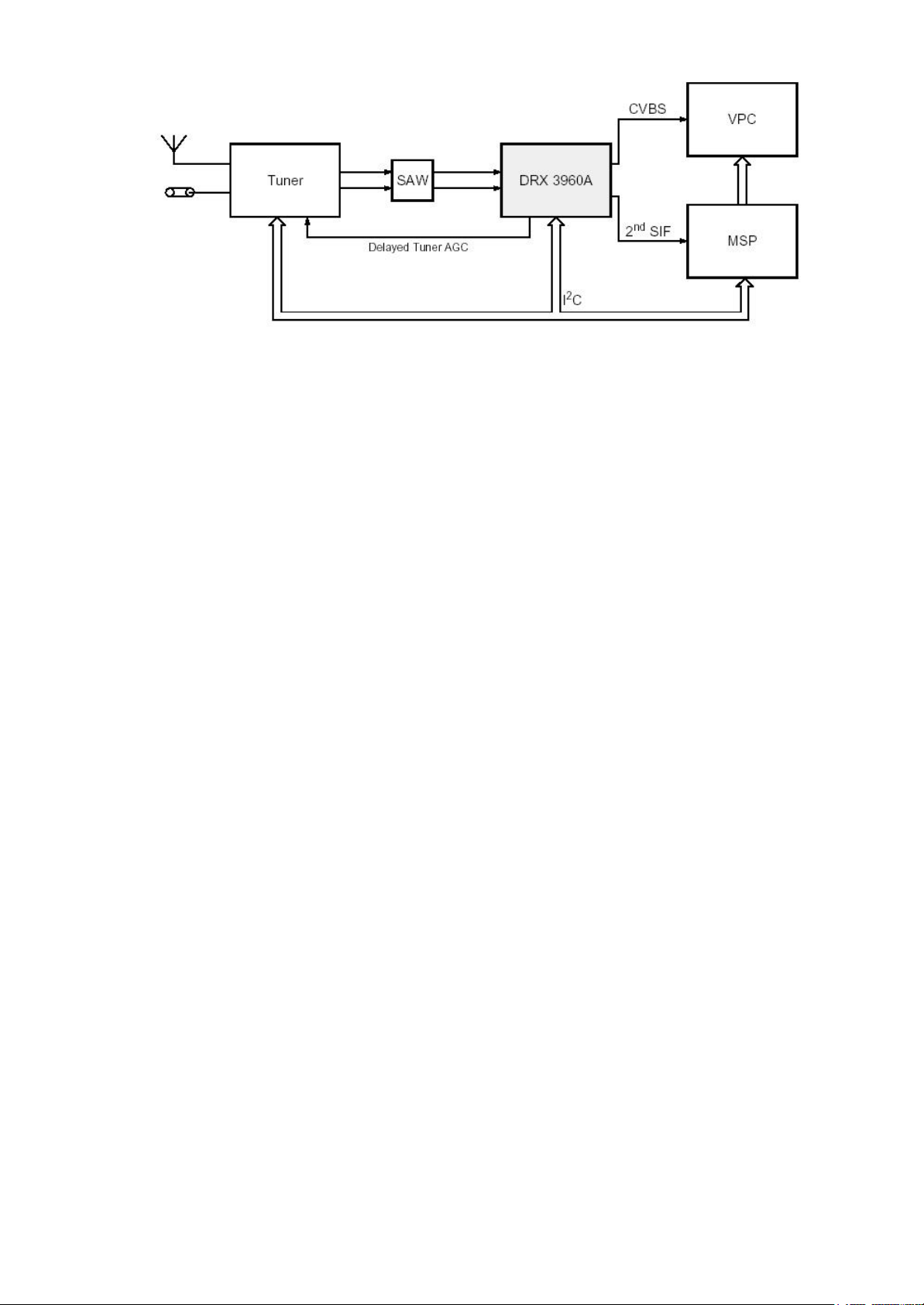
3.IF PART (DRX 3960A)
Tuner output IF signal is pre -filtered with only one 8-MHz channel SAW filter. The entire multistandard
processing is performed. The Digital Receiver Front -end DRX 3960A performs the entire multi-standard
Quasi Split Sound (QSS) TV IF processing, AGC, video demodulation, and generation of the second
sound IF (SIF). Video and tuner AGC is controlled and adjusted by take over voltage. The alignment free DRX 3960A needs no special external components. All control functions and status registers are
accessible via I2C bus interface.
1
4.VIDEO SWITCH TEA6415
In case of three or more external sources are used, the video switch IC TEA6415 is used. The main
function of this device is to switch 8 video-input sources on the 6 outputs.
Each output can be switched on only one of each input. On each input an alignme nt of the lowest level
of the signal is made (bottom of sync. top for CVBS or black level for RGB signals).
Each nominal gain between any input and output is 6.5dB.For D2MAC or Chroma signal the alignment
is switched off by forcing, with an external resistor bridge, 5VDC on the input. Each input can be used
as a normal input or as a MAC or Chroma input (with external Resistor Bridge). All the switching
possibilities are changed through the BUS. Driving 75ohm load needs an external resistor. It is possible
to have the same input connected to several outputs.
5.MULTI STANDARD SOUND PROCESSOR
The MSP34x1G family of single -chip Multi-standard Sound Processors covers the sound processing of
all analog TV -Standards worldwide, as well as the NICAM digital sound standards. The full TV sound
processing, starting with analog sound IF signal-in, down to processed analog AF-out, is performed on
a single chip. Signal conforming to the standard by the Broadcast Television Systems Committee
(BTSC).
The DBX noise reduction, or alternatively, MICRONAS Noise Reduction (MNR) is performed alignment
free. Other processed standards are the Japanese FM-FM multiplex standard (EIA-J) and the FM
Stereo Radio standard.
6.SOUND OUTPUT STAGE WITH TDA7480L
The TDA7480L is an audio class-D amplifier assembled in Power DIP package specially designed for
high efficiency applications mainly for TV and Home Stereo sets.
Mute stand-by function of the audio amplifier can be described as the following; the pin 12
(MUTE/STAND-BY) controls the amplifier status by two different thresholds, referred to ground. When
Vpin 12 voltage is lower than 0.7V the amplifier is in Stand-by mode and the final stage generators are
off. When Vpin 12 is higher than 4V, the amplifier is in play mode.
The TDA7480L is a 10W+10W stereo sound amplifier with mute/stand -by facility. MUTE control signal
coming from microcontroller (when it is at high level) activates the mute function. IC is muted when
mute pin is at low level (pin12). MUTE pin can also be activated via an external pop-noise circuitry in
order to eliminate pop noise when TV is turned off. Just after the TV is turned off, this circuit switches
the IC to stand-by mode by pulling the mute pin voltage to ground.
7.VERTICAL OUTPUT STAGE WITH TDA8177F
The IC TDA8177F is the vertical deflection booster circuit. Two supply voltages, +12V and -12V are
needed to scan the inputs VERT+ and VERT-, respectively. And a third supply voltage, +60V for the
flyback limiting are needed. The vertical deflection coil is connected in series between the output and
feedback to the input.
8.VIDEO OUTPUT AMPLIFIER TDA6109
The TDA6109 includes three video output amplifiers in order to drive the three cathodes of a colour
picture tube directly. To obtain maximum performance, the amplifier is used with black-current control.
2

9.POWER SUPPLY (SMPS)
The DC voltages required at various parts of the chassis are provided by an SMPS transformer
controlled by the IC MC44608, which is designed for driving, controlling and protecting switching
transistor of SMPS. The transformer generates 135V for FBT input, +/-14V for audio amplifier, 8V stand
by voltage and 8V, 12V and 5V supplies for other different parts of the chassis.
An optocoupler is used to control the regulation of line voltage and stand-by power consumption. There
is a regulation circuit in secondary side. This circuit produces a control voltage according to the
changes in 135V DC voltage, via an optocoupler (TCET 1102G) to pin3 of the IC.
During the switch on period of the transistor, energy is stored in the transformer. During the switch off
period energy is fed to the load via secondary winding. By varying switch-on time of the power
transistor, it controls each portion of energy transferred to the second side such that the output voltage
remains nearly independent of load variations.
10.MICROCONTROLLER SDA5550
10.1.General Features
• Feature selection via special function register
• Simultaneous reception of TTX, VPS, PDC, and WSS (line 23)
• Supply Voltage 2.5 and 3.3 V
• ROM version is used.
10.2.External Crystal and Programmable Clock Speed
• Single external 6MHz crystal, all necessary clocks are generated internally
• CPU clock speed selectable via special function registers.
• Normal Mode 33.33 MHz CPU clock, Power Save mode 8.33 MHz
10.3.Microcontroller Features
• 8bit 8051 instruction set compatible CPU.
• 33.33-MHz internal clock (max.)
• 0.360 ms (min.) instruction cycle
• Two 16 -bit timers
• Watchdog timer
• Capture compare timer for infrared remote control decoding
• Pulse width modulation unit (2 channels 14 bit, 6 channels 8 bit)
• ADC (4 channels, 8 bit)
• UART (rxd, txd)
10.4.Memory
• Up to 128 Kilobyte on Chip Program ROM
• Eight 16-bit data pointer registers (DPTR)
• 256-bytes on-chip Processor Internal RAM (IRAM)
• 128bytes extended stack memory.
• Display RAM and TXT/VPS/PDC/WSS-Acquisition-Buffer directly accessible via MOVX
• UP to 16KByte on Chip Extended RAM (XRAM) consisting of;
- 1 Kilobyte on -chip ACQ-buffer-RAM (access via MOVX)
- 1 Kilobyte on -chip extended-RAM (XRAM, access via MOVX) for user software
- 3 Kilobyte Display Memory
10.5.Display Features
• ROM Character set supports all East and West European Languages in single device
• Mosaic Graphic Character Set
• Parallel Display Attributes
• Single/Double Width/Height of Characters
• Variable Flash Rate
• Programmable Screen Size (25 Rows x 33...64 Columns)
• Flexible Character Matrixes (HxV) 12 x 9...16
• Up to 256 Dynamical Redefinable Characters in standard mode; 1024 Dynamical Redefinable
Characters in Enhanced Mode
• CLUT with up to 4096 colour combinations
• Up to 16 Colours per DRCS Character
• One out of 8 Colours for Foreground and Background Colours for 1-bit DRCS and ROM Characters
10.6.ROM Characters
• Shadowing
• Contrast Reduction
• Pixel by Pixel Shiftable Cursor With up to 4 Different Colours
• Support of Progressive Scan and 100 Hz.
3

• 3 X 4Bits RGB-DACs On -Chip
• Free Programmable Pixel Clock from 10 MHz to 32MHz
• Pixel Clock Independent from CPU Clock
• Multinorm H/V-Display Synchronization in Master or Slave Mode
10.7.Acquisition Features
• Multi-standard Digital Data Slicer
• Parallel Multi-norm Slicing (TTX, VPS, WSS, CC, G+)
• Four Different Framing Codes Available
• Data Caption only limited by available Memory
• Programmable VBI-buffer
• Full Channel Data Slicing Supported
• Fully Digital Signal Processing
• Noise Measurement and Controlled Noise Compensation
• Attenuation Measurement and Compensation
• Group Delay Measurement and Compensation
• Exact Decoding of Echo Disturbed Signals
10.8.Ports
• One 8-bit I/O-port with open drain output and optional I2C Bus emulation support (Port0)
• Two 8-bit multifunction I/O-ports (Port1, Port3)
• One 4-bit port working as digital or analogue inputs for the ADC (Port2)
• One 2-bit I/O port with secondary function (P4.2, 4.3, 4.7)
• One 4-bit I/O-port with secondary function (P4.0, 4.1, 4.4) (Not available in P-SDIP 52)
11.SERIAL ACCESS 32K EEPROM
24LC32 is the 32Kbit electrically erasable programmable memory. The memory is compatible with the
I2C standard, two wire serial interface, which uses a bi -directional data bus and serial clock.
12.CLASS AB STEREO HEADPHONE DRIVER TDA1308
The TDA1308 is an integrated class AB stereo headphone driver contained in a DIP8 plastic package.
The device is fabricated in a 1 mm CMOS process and has been primarily developed for portable digital
audio applications.
13.SAW FILTERS
X6966M is an 8-MHz SAW Filter which is used for pre-filtering the IF input signal of DRX 3960A. The
entire multistandard processing is performed within this filter which limits the signal bandwidth to 8 MHz
and suppresses major parts of the adjacent channels.
14.IC DESCRIPTIONS
TDA6109
27W401
24LC32
SDA5275
DRAM 4MX4
SDA9400
LM317T
DDP3310
SDA5550
TEA6415
VPC3230D
TDA1308T
MSP3411G
TL431
DRX3960A
LM7808
BDX53BFI
TDA8177F
LM1086
MC44608
TCET1102G
TDA7480L
SAA3010T
4

14.1.TDA6109
14.1.1.General Description
The TDA6109JF includes three video output amplifiers in one plastic DIL-bent-SIL 9-pin medium power
(DBS9MPF) package (SOT111-1), using high-voltage DMOS technology, and is intended to drive the three
cathodes of a colour CRT directly. To obtain maximum performance, the amplifier should be used with blackcurrent control.
14.1.2.Features
· Typical bandwidth of 9.0 MHz for an output signal of 60 V (p-p)
· High slew rate of 1850 V/ms
· No external components required
· Very simple application
· Single supply voltage of 200 V
· Internal reference voltage of 2.5 V
· Fixed gain of 51
· Black-Current Stabilization (BCS) circuit
· Thermal protection.
14.1.3.Pinning
SYMBOL PIN DESCRIPTION
V
1 inverting input 1
i(1)
V
2 inverting input 2
i(2)
V
3 inverting input 3
i(3)
GND 4 ground (fin)
Iom 5 black current measurement output
VDD 6 supply voltage
V
7 cathode output 3
oc(3)
V
8 cathode output 2
oc(2)
V
9 cathode output 1
oc(1)
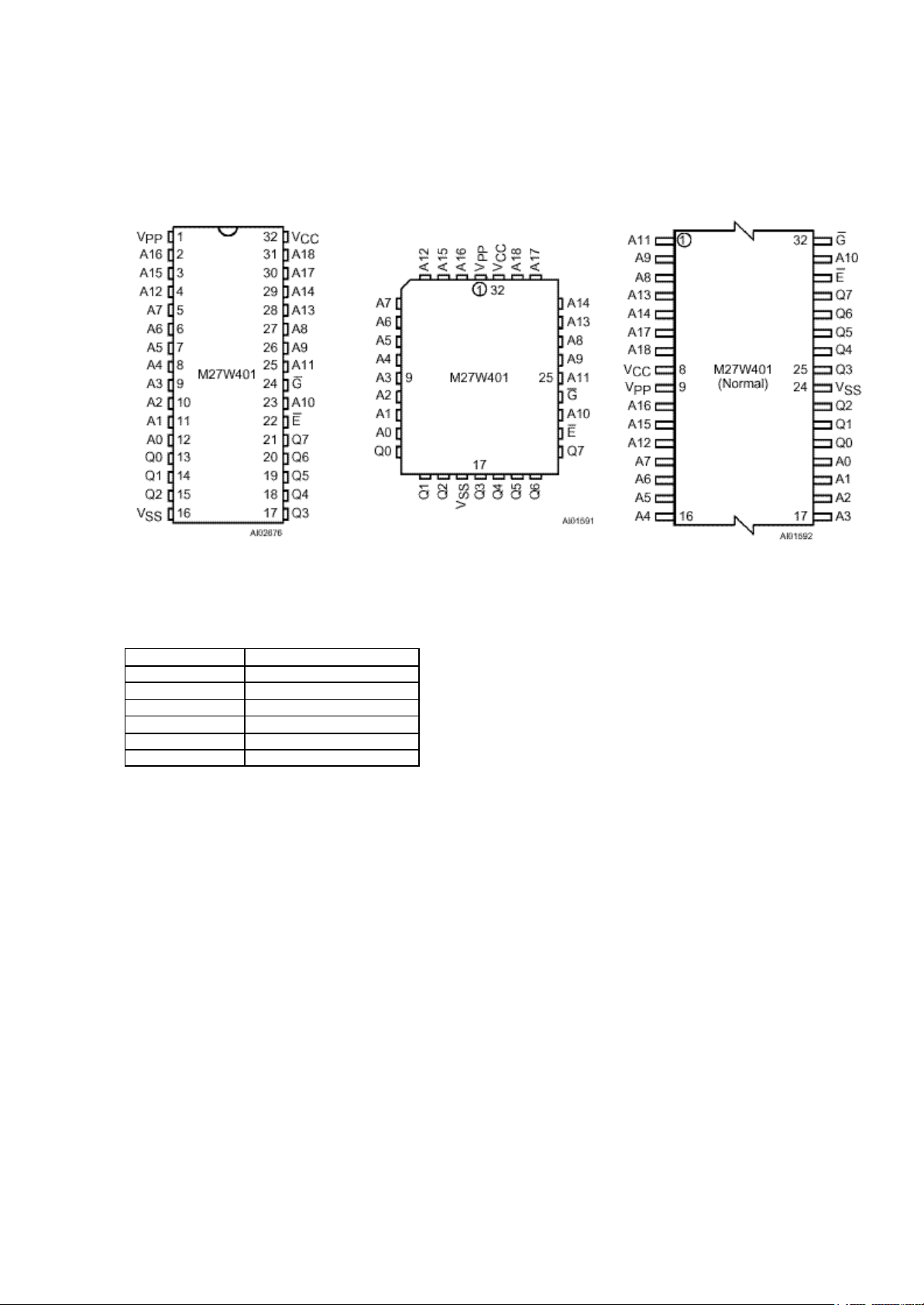
14.2.27W401
14.2.1.Description
The M27W401 is a low voltage 4 Mbit EPROM offered in the two ranges UV (ultra violet erase) and
OTP (one time programmable). It is ideally suited for microprocessor systems requiring large data or
program storage and is organized as 524,288 by 8 bits. The M27W401 operates in the read mode with
a supply voltage as low as 2.7V at –40 to 8??C temperature range. The decrease in operating power
allows either a reduction of the size of the battery or an increase in the time between battery recharges.
The FDIP32W (window ceramic frit-seal package) has a transparent lid, which allows the user to ex pose the chip to ultraviolet light to erase the bit pat-tern. A new pattern can then be written to the
device by following the programming procedure. For application where the content is programmed only
one time and erasure is not required, the M27W401 is offered in PDIP32, PLCC32 and TSOP32 (8 x 20
mm) packages.
14.2.2.Features
2.7V to 3.6v Low voltage in Read Operation
Access time:
–70ns at V
–80ns at V
= 3.0V to 3.6V
CC
= 2.7V to 3.6V
CC
Pin Compatible with M27C4001
Low Power Consumption:
–1?mA max Standby Current
– 15mA max Active Current at 5MHz
Programming Time 10?ms/byte
High Reliability CMOS Technology
– 2,000V ESD Protection
– 200mA Latchup Protection Immunity
5
Electronic Signature
– Manufacturer Code: 20h
– Device Code: 41h
14.2.3.Connections
DIP connections LCC Connections TSOP Connections
Signal Names
A0-A18 Address Inputs
Q0-Q7 Data Outputs
E Chip Enable
G Output Enable
Vpp Program Supply
Vcc Supply Voltage
Vss Ground
14.3.24LC32A
14.3.1.Description
The Microchip Technology Inc. 24LC32A is a 4K x 8 (32K bit) Serial Electrically Erasable PROM
capable of operation across a broad voltage range (2.5V to 6.0V). It has been developed for advanced,
low power applications such as personal communications or data acquisition. The 24LC32A also has a
page-write capability of up to 32 bytes of data. The 24LC32A is capable of both random and sequential
reads up to the 32K boundary. Functional address lines allow up to eight 24LC32A devices on the
same bus, for up to 256K bits address space. Advanced CMOS technology and broad voltage range
make this device ideal for low-power/ low-voltage, nonvolatile code and data applications. The
24LC32A is available in the standard 8-pin plastic DIP and both 150 mil and 200 mil SOIC packaging.
14.3.2.Features
• Single supply with operation down to 2.5V
• Maximum write current 3 mA at 6.0V
• Standby current 1 mA max at 2.5V
• 2-wire serial interface bus, I 2 CÔ compatible
• 100 kHz (2.5V) and 400 kHz (5V) compatibility
• Self-timed ERASE and WRITE cycles
• Power on/off data protection circuitry
• Hardware write protect
• 1,000,000 Erase/Write cycles guaranteed
• 32 byte page or byte write modes available
6

• Schmitt trigger filtered inputs for noise suppression
• Output slope control to eliminate ground bounce
• 2 ms typical write cycle time, byte or page
• Up to eight devices may be connected to the same bus for up to 256K bits total memory
• Electrostatic discharge protection > 4000V
• Data retention > 200 years
• 8-pin PDIP and SOIC packages
• Temperature ranges
• Commercial (C): 0°C to +75°C
• Industrial (I): -40°C to +85°C
14.3.3.Pin Descriptions
A0, A1, A2 Chip Address Inputs
The A0..A2 inputs are used by the 24LC32A for multiple device operation and conform to the 2-wire bus
standard. The levels applied to these pins define the address block occupied by the device in the
address map. A particular device is selected by transmitting the corresponding bits (A2, A1, A0) in the
control byte.
SDA Serial Address/Data Input/Output
This is a Bi -directional pin used to transfer addresses and data into and data out of the device. It is an
open drain terminal, therefore the SDA bus requires a pull up resistor to VCC (typical 10 kO for 100 kHz,
2 kO for 400 kHz) For normal data transfer SDA is allowed to change only during SCL low. Changes
during SCL HIGH are reserved for indicating the START and STOP conditions.
SCL Serial Clock
This input is used to synchronize the data transfer from and to the device.
WP
This pin must be connected to either VSS or VCC. If tied to VSS, normal memory operation is enabled
(read/write the entire memory 000-FFF). If tied to VCC, WRITE operations are inhibited. The entire
memory will be write-protected. Read operations are not affected.
WCC
+2.5V to 6V Power Supply
WSS
Ground
14.4.SDA5275
14.4.1.Features
• Single chip teletext IC
• Analog CVBS-input with onchip clamping circuitry
• Slicer
• Supports level 1, 2.5 and 3.5 ETSI teletext standard
• Stores up to 14 teletext pages on chip
• Stores up to 2048 teletext pages with external 16 M memory
• SDA 5275: full level 2.5 processing
• Analog RGB-output
• 41 Latin script languages
• 12 ´ 10 character size
• Parallel display attributes
• 64 fro m 4096 colors selectable
• Enhanced flash modes
• Dynamically redefinable character set (DRCS, PCS)
• Pixel graphics
• Full screen display (64 ´ 32 or 80 ´ 24 character positions)
• Horizontal and vertical scrolling
• Graphic cursors
• 4:3 and 16:9 display
• Multinorm display (50/60/100/120 Hz)
• RISC-processor
• Firmware downloadable
• I2C / 3 wire UART-interface (1 Mbit/s)
• Independent clocks for acquisition and display
7

• Tools for greatly simplified software development
• 24-Kbyte on -chip reconfigurable DRAM
• 44160 -bit character ROM
• One external crystal for all standards
14.4.2.Pin Definition and functions
Pin No. P-LCC-68-1 Symbol Function
1 INTQ Interrupt request output to ext. controller
2 CLK-IO System clock input/output
3 TCSQ/FLD Composite sync output/ field output
4 VS/VCS Vertical sync input/output
5 HS Horizontal sync input/output
6 XOUT 20.5-MHz crystal oscillator output
7 XIN 20.5-MHz crystal oscillator input
8 GPO General purpose output
9 TM Test pin, leave open or connect VSS
10 CVBS CVBS-video signal input
11 VDD1 + 5 V digital supply
12 VDDA + 5 V analog supply
13 VSSA1 Analog ground
14 N.C. Not connected
15 N.C. Not connected
16 VDD2 + 5 V digital supply
17 RES Chip reset
18 N.C. Not connected
19 N.C. Not connected
20 N.C. Not connected
21 VDD3 + 5 V digital supply
22 N.C. Not connected
23 VREF + 3 V reference voltage input
24 N.C. Not connected
25 VDD4 + 5 V digital supply
26 A8 External DRAM -address
27 A7 External DRAM -address
28 A6 External DRAM -address
29 A5 External DRAM -address
30 A4 External DRAM -address
31 A3 External DRAM -address
32 A2 External DRAM -address
33 A1 External DRAM -address
34 A0 External DRAM -address
35 A9 External DRAM -address
36 A10 External DRAM -address
37 A11 External DRAM -address
38 RASQ Row address strobe (DRAM)
39 WEQ Write enable (DRAM)
40 D1 External DRAM -data
41 D0 External DRAM -data
42 D2 External DRAM -data
43 D3 External DRAM -data
44 VSS4 0 V digital supply
45 CASQ Column address strobe
46 N.C. Not connected
47 N.C. Not connected
48 N.C. Not connected
49 VSS3 0 V digital supply
50 N.C. Not connected
51 N.C. Not connected
52 N.C. Not connected
53 N.C. Not connected
54 N.C. Not connected
55 VSS2 0 V digital supply
56 VBB Substrate bias voltage N.C.* (depends on version)
57 N.C. Not connected
8

58 VSSA2 Analog ground
59 RGB-GND RGB-ground
60 VSS1 0 V digital supply
61 R Analog red display output
62 G Analog green display output
63 B Analog blue display output
64 BLAN Blanking signal open drain output
65 CORQ Contrast reduction open drain output
66 SCL Bi-directional I2C Bus clock port
67 SDA Bi-directional I2C Bus data port
68 I2CEN I2C Bus enable
14.5.DRAM 4MX4
14.5.1.General Description
The 4 Meg x 4 DRAM is a randomly accessed, solid-state memory containing 16,777,216 bits
organized in a x4 con-figuration. RAS# is used to latch the row address (first 11 bits for 2K and first 12
bits for 4K). Once the page has been opened by RAS#, CAS# is used to latch the column address (the
latter 11 bits for 2K and the latter 10 bits for 4K, address pins A10 and A11 are “don’t care”). READ and
WRITE cycles are selected with the WE# input. A logic HIGH on WE# dictates READ mode, while a
logic LOW on WE# dictates WRITE mode. During a WRITE cycle, data-in (D) is latched by the falling
edge of WE# or CAS#, whichever occurs last. An EARLY WRITE occurs when WE# is taken LOW prior
to CAS# falling. A LATE WRITE or READ-MODIFY-WRITE occurs when WE# falls after CAS# is taken
LOW. During EARLY WRITE cycles, the data outputs (Q) will remain High-Z regardless of the state of
OE#. During LATE WRITE or READ-MODIFY -WRITE cycles, OE# must be taken HIGH to disable the
data outputs prior to applying input data. If a LATE WRITE or READ-MODIFY-WRITE is attempted
while keeping OE# LOW, no write will occur, and the data outputs will drive read data from the
accessed location. The four data inputs and the four data outputs are routed through four pins usin g
common I/O, and pin direction is controlled by WE# and OE#.
14.5.2.Features
• Industry -standard x4 pin out, timing, functions and packages
• State-of-the-art, high-performance, low -power CMOS silicon-gate process
• Single power supply (+3.3V ±0.3V or +5V ±10%)
• All inputs, outputs and clocks are TTL-compatible
• Refresh modes: RAS#-ONLY, HIDDEN and CAS#-BEFORE- RAS# (CBR)
• Optional Self Refresh (S) for low-power data retention
• 11 row, 11 column addresses (2K refresh) or 12 row, 10 column addresses (4K refresh)
• Extended Data-Out (EDO) PAGE MODE access cycle
• 5V -tolerant inputs and I/Os on 3.3V devices
14.5.3.Pin Assignment
Top View
*NC on 2K refresh and A11 on 4K refresh options. Note: The “#” symbol indicates signal is active LOW.
9

14.6.SDA9400
14.6.1.General Description
The SDA9400 is a new component of the Micronas MEGAVISION ® IC set in a 0.35µm embedded
DRAM technology (frame memory embedded). The SDA9400 is pin compatible to the SDA9401 (field
memory embedded). The SDA9400 comprises all main functionalities of a digital feature box in one
monolithic IC. The scan rate conversion to 100/120 Hz interlaced (50/60 Hz progressive) is based on a
motion adaptive algorithm. The scan rate converted picture can be vertically expanded. The SDA9400
has a free running mode, therefore features like scan rate conversion to e.g. 70, 75 Hz with joint lines or
multiple picture display (e.g. tuner scan) are possible. Due to the frame based signal processing, the
noise reduction has been greatly improved. Furthermo re separate motion detectors for luminance and
chrominance have been implemented. For automatic controlling of the noise reduction parameters a
noise measurement algorithm is included, which measures the noise level in the picture or in the
blanking period. In addition a spatial noise reduction is implemented, which reduces the noise even in
the case of motion. The input signal can be compressed horizontally and vertically with a certain
number of factors. Therefore split screen is supported. Beside these additional functions like coloured
background, windowing and flashing are implemented.
14.6.2.Features
• Two input data formats
- 4:2:2 luminance and chrominance parallel (2 x 8 wires)
- ITU-R 656 data format (8 wires)
• Two different representations of input chrominance data
- 2‘s complement code
- Positive dual code
• Flexible input sync controller
• Flexible compression of the input signal
- Digital vertical compression of the input signal (1.0, 1.25, 1.5, 1.75, 2.0, 3.0, 4.0)
- Digital horizontal compres sion of the input signal (1.0, 2.0, 4.0)
• Noise reduction
- Motion adaptive spatial and temporal noise reduction (3D-NR)
- Temporal noise reduction for luminance frame based or field based
- Temporal noise reduction for chrominance field based
- Separate motion detectors for luminance and chrominance
- Flexible programming of the temporal noise reduction parameters
- Automatic measurement of the noise level (5 -bit value, readable by I²C bus)
• 3-D motion detection
- High performance motion detector for scan rate conversion
- Global motion detection flag (readable by I²C bus)
- Movie mode and phase detector (readable by I²C bus)
• TV mode detection by counting line numbers (PAL, NTSC, readable by I²C bus)
• Embedded memory
- 5 Mbit embedded DRAM core for field memories
- 192 kbit embedded DRAM core for line memories
• Flexible clock and synchronization concept
- Decoupling of the input and output clock system possible
• Scan rate conversion
- Motion adaptive 100/120 Hz interlaced scan conversion
- Motion adaptive 50/60 Hz progressive scan conversion
- Simple static interlaced and progressive conversion modes for 100/120 Hz interlaced or 50/60 Hz
progressive scan conversion: e.g. ABAB, AABB, AA*B*B, AAAA, BBBB, AB, AA*
- Simple progressive scan conversion with joint lines:
50 Hz -> 60, 70, 75 Hz progressive
60 Hz -> 70, 75 Hz progressive
- Large area and line flicker reduction
• Flexible digital vertical expansion of the output signal (1.0, ... [1/32] ..., 2.0)
• Flexible output sync controller
- Flexible positioning of the output signal
- Flexible programming of the output sync raster
- External synchronization by backend IC possible
(e.g. split screen for one TV channel with joint lines and one PC VGA channel)
10

• Signal manipulations
- Insertion of coloured bac kground
- Vertical and/or horizontal windowing with four different speed factors
- Flash generation (for supervising applications, motion flag readable by I²C bus)
- Still frame or field
- Support of split screen applications
- Multiple picture display - Tuner scan (4 and 16 times for 4:3, 12 times for 16:9 tubes)
- Support of multi picture display with PIP or front-end processor with integrated scaler
(e.g. 9 times display of PIP pictures, picture tracking, random pictures, still-in-moving picture, moving in-still picture)
• I²C -bus control (400 kHz)
• P-MQFP-64 package
• 3.3 V ± 5% supply voltage
14.6.3.Pin Definition
Pin No. Name Type Description
2,8,24,42,55 VSS1 S Supply voltage ( V SS = 0 V )
9,25,41,56 VDD1 S Supply voltage ( V DD = 3.3 V )
36,52,58 VSS2 S Supply voltage ( V SS = 0 V )
35,51,53,57,59 VDD2 S Supply voltage ( V DD = 3.3 V )
43,..,50 YIN0...7 I/TTL Data input Y (see input data format)
31,..,34;37,...,40 UVIN0...7 I/TTL
PD
30 RESET I/TTL System reset. The RESET input is low active. In order to ensure
23 HIN I/TTL
PD
22 VIN I/TTL
29 SYNCEN I/TTL Synchronization enable input
21 SDA I/O I2C-Bus data line (5V ability)
20 SCL I I I2C-Bus clock line (5V ability)
54 CLK1 I/TTL System clock 1
17,..,10 UVOUT0...7 O/TTL Data output UV (see output data format)
7,..,3;1;64;63 YOUT0...7 O/TTL Data output Y (see output data format)
62 HREF O/TTL Horizontal active video output
61 VOUT/
VEXT
60 HOUT/
HEXT
18 INTERLACED O/TTL Interlace signal for AC coupled vertical deflection
28 X1 / CLK2 I/TTL Crystal connection / System clock 2
27 X2 O/AN Crystal connection
26 CLKOUT O/TTL Clock output (depends on I²C parameters CLK11EN, CLK21EN,
19 TEST I/TTL Test input, connect to V SS for normal operation
PD
I/O/
TTL
I/O/
TTL
Data input UV (for 4:2:2 parallel, see input data format)
(for CCIR 656, see input data format)
correct operation a "Power On Reset" must be performed. The
RESET pulse must have a minimum duration of two clock periods
of the system clock CLK1.
H-Sync input
(only for full CCIR 656)
V-Sync input
(only for full CCIR 656)
EXSYN=0 (I²C-bus par ameter): V-Sync output
EXSYN=1: External V -Sync input for output part
EXSYN=0 (I²C-bus parameter): H-Sync output
EXSYN=1: External H-Sync input for output part
FREQR)
14.7.LM317T
14.7.1.Description
The LM317T is an adjustable 3 terminal positive voltage regulator capable of supplying in excess of 1.5
amps over an output range of 1.25 to 37 volts. This voltage regulator is exceptionally easy to use and
requires only two external resistors to set the output voltage. Further, it employs internal current limiting,
thermal shutdown and safe area compensation, making it essentially blow–out proof. The LM317
serves a wide variety of applications including local, on card regulation. This device can also be used to
make a programmable output regulator, or by connecting a fixed resistor between the adjustment and
output, the LM317 can be used as a precision current regulator.
14.7.2.Features
• Output Current in Excess of 1.5 A
11

• Output Adjustable bet ween 1.2 V and 37 V
• Internal Thermal Overload Protection
• Internal Short Circuit Current Limiting Constant with Temperature
• Output Transistor Safe–Area Compensation
• Floating Operation for High Voltage Applications
• Available in Surface Mount D2PAK, and Standard 3–Lead Transistor Package
• Eliminates Stocking many Fixed Voltages
14.8.DDP3310
14.8.1.Description
The DDP 3310B is a single-chip digital Display and Deflection Processor designed for high-quality
back-end applications in 100/120-Hz TV sets with 4:3 or 16:9 picture tubes. The IC can be combined
with members of the DIGIT 3000 IC family (VPC 32xx, TPU 3040), or it can be used with third-party
products. The IC contains the entire digital video component and deflection processing and all analog
interface components.
14.8.2.Features
Video processing
– linear horizontal scaling (0.25 … 4)
– non -linear horizontal scaling “panorama-vision”
– dynamic peaking
– soft limiter (gamma correction)
– color transient improvement
– programmable RGB matrix
– picture frame generator
– two analog RGB/Fast-Blank inputs. The DDP 3310B is a single-chip digital Display and Deflection
Processor designed for high -quality back-
Deflection processing
– scan velocity modulation output
– high -performance H/V deflection
– EHT compensation for vertical / East/West
– soft start/stop of H-Drive
– vertical angle and bow
– differential vertical output
– vertical zoom via deflection
– horizontal and vertical protection circuit
– adjustable horizontal frequency for VGA/SVGA display
Miscellaneous
– selectable 4:1:1/ 4:2:2 YC r C b input
– selectable 27/ 32-MHz line -locked clock input
– crystal oscillator for horizontal protection
– automatic picture tube adjustment (cutoff, white-drive)
– single 5-V power supply
– hardware for simple 50/60 -Hz to 100/ 120-Hz conversion (display frequency doubling)
– two I2C-controlled PWM outputs
– beam current limiter
14.8.3.Pin connection and short descriptions
NC = not connected LV = if not used, leave vacant
X = obligatory; connect as described in circuit diagram IN = Input
OUT = Output SUPPLY = Supply Pin
Pin no
PLCCK 68 pin
1 VSUPP SUPPLY X Supply voltage, Output pin driver
2 GNDP SUPPLY X Ground, Output pin driver
3 VS2 IN GNDD Additional VSYNC input
4 FIFORRD OUT LV FIFO Read counter reset
Pin name Type Connection
(if not used)
Short description
12

5 FIFORD OUT LV FIFO Read Enable
6 FIFOWR OUT LV FIFO Write Enable
7 FIFORWR OUT LV FIFO Write counter reset
8 HOUT OUT X Horizontal Drive Output
9 HFLB IN Hout Horizontal Flyback Input
10 SAFETY IN GNDO Safety Input
11 VPROT IN GNDO Vertical protection Input
12 FREQSEL IN X Selection of H-Drive Frequency Range
13 CM1 IN X Clock select 40.5 or 27/32 MHz
14 CMO IN X Clock select 27/32 MHz
15 RSW2 OUT LV Range Switch2, Measurement ADC
16 RSW1 IN/OUT LV Range Switch1, Measurement ADC
17 SENSE IN GNDO Sense ADC Input
18 GNDM SUPPLY X Ground, MADC Input
19 VERT+ OUT GNDO Differantial Vertical Sawtooth Output
20 VERT- OUT GNDO Differantial Vertical Sawtooth Output
21 EW OUT GNDO Vertical Parabola Output
22 XREF IN X Reference Input for RGB DACs
23 SVM OUT VSUPO Scan Velocity Modulation
24 ROUT OUT VSUPO Analog Output Red
25 GOUT OUT VSUPO Analog Output Green
26 BOUT OUT VSUPO Analog Output Blue
27 GNDO SUPPLY X Ground, Analog Back-end
28 VSUPO SUPPLY X Supply Voltage, Analog Back-end
29 VRD/BCS IN X DAC Reference, Beam Current Safety
30 FBLIN1 IN GNDO Fast-Blank1 Input
31 RIN1 IN GNDO Analog Red1 Input
32 GIN1 IN GNDO Analog Green1 Input
33 BIN1 IN GNDO Analog Blue1 Input
34 FBLIN2 IN GNDO Fast-Blank2 Input
35 RIN2 IN GNDO Analog Red2 Input
36 GIN2 IN GNDO Analog Green2 Input
37 BIN2 IN GNDO Analog Blue2 Input
38 TEST IN GNDD Test Pin
39 RESQ IN X Reset Input, active low
40 PWM1 OUT LV I2C-controlled DAC
41 PWM2 OUT LV I2C-controlled DAC
42 HCS IN GNDD Half-contrast
43 C0 IN GNDD Picture Bas Chroma (LSB)
44 C1 IN GNDD Picture Bas Chroma
45 C2 IN GNDD Picture Bas Chroma
46 C3 IN GNDD Picture Bas Chroma
47 C4 IN GNDD Picture Bas Chroma
48 C5 IN GNDD Picture Bas Chroma
49 C6 IN GNDD Picture Bas Chroma
50 C7 IN GNDD Picture Bas Chroma (MSB)
51 VSUPD SUPPLY X Supply Voltage, Digital Circuitry
52 GNDD SUPPLY X Ground, Digital Circuitry
53 LLC2 IN X System Clock Input (27/32/40.5 MHz)
54 Y0 IN GNDD Picture Bas Luma (LSB)
55 Y1 IN GNDD Picture Bas Luma
56 Y2 IN GNDD Picture Bas Luma
57 Y3 IN GNDD Picture Bas Luma
58 Y4 IN GNDD Picture Bas Luma
59 Y5 IN GNDD Picture Bas Luma
60 Y6 IN GNDD Picture Bas Luma
61 Y7 IN GNDD Picture Bas Luma (MSB)
62 LLC1 IN VSUPD Single Line-Locked Clock Input (13.5/16 MHz)
63 HS IN X Horizontal Sync Input
64 VS IN GNDD Vertical Sync Input
65 XTALK2 OUT X Analog Crystal Output (5-MHz Security Clock)
66 XTALK1 IN X Analog Crystal Input (5-MHz Security Clock)
67 SDA IN/OUT X I2C-Bus Data
68 SCL IN/OUT X I2C-Bus Clock
13

14.9.SDA5550
14.9.1.General definition
The SDA5550M is a single chip teletext decoder for decoding World System Teletext data as well as
Video Programming System (VPS), Program Delivery Control (PDC), and Wide Screen Signalling
(WSS) data used for PAL plus transmissions (Line 23). The device provides an integrated generalpurpose, fully 8051-compatible Microcontroller with television specific hardware features.
Microcontroller has been enhanced to provide powerful features such as memory banking, data
pointers, and additional interrupts etc. The on-chip display unit for displaying Level 1.5 teletext data can
also be used for customer defined on screen displays. Internal XRAM consists of up to 17 Kbytes. This
device can support external memory up to 1Mbyte ROM and RAM.TVTEXT Controller contains a data
slicer for VPS, WSS, PDC and TXT, an acceleration acquisition hardware module, a display generator
for Level 1.5 TXT and powerful On screen Display capabilities based on parallel attributes, and pixel
oriented characters (DRCS). The 8 bit Microcontroller operates at 360nsec cycle time (min). Controller
with dedicated hardware does most of the internal TXT acquisition processing, transfer data to/from
external memory interface and receives/transmits data via I2C-firmware user interface. SDA5550M is
realized in 0.25 micron technology with 2.5V supply voltage and 3.3V I/O compatible. The IC produces
the following input or output control signals; AGC_CON, MODE_SW, L / L’, PIP_MODS, PIP_SEL,
ON/OFF (stand-by), SC1..3_IN_AV (pin 8 information from 3 SCARTs), AFC, MUTE (to mute audio
output IC), I2CEN.
14.9.2.Features
General
• Feature selection via special function register
• Simultaneous reception of TTX, VPS, PDC, and WSS (line 23)
• Supply Voltage 2.5 and 3.3 V
External Crystal and Programmable clock speed
Single external 6MHz crystal, all necessary clocks are generated internally
CPU clock speed selectable via special function registers.
Normal Mode 33.33 MHz CPU clock, Power Save mode 8.33 MHz
Microcontroller Features
• 8bit 8051 instruction set compatible CPU.
• 33.33-MHz internal clock (max.)
• 0.360ms (min.) instruction cycle
• Two 16 -bit timers
• Watchdog timer
• Capture compare timer for infrared remote control decoding
• Pulse width modulation unit (2 channels 14 bit, 6 channels 8 bit)
• ADC (4 channels, 8 bit)
• UART
Memory
• Non-multiplexed 8-bit data and 16 … 20 -bit address bus (ROMless Version)
• Memory banking up to 1Mbyte (Romless version)
• Up to 128 Kilobyte on Chip Program ROM
• Eight 16-bit data pointer registers (DPTR)
• 256-bytes on-chip Processor Internal RAM (IRAM)
• 128bytes extended stack memory.
• Display RAM and TXT/VPS/PDC/WSS-Acquisition-Buffer directly accessible via MOVX
• UP to 16KByte on Chip Extended RAM (XRAM) consisting of;
- 1 Kilobyte on -chip ACQ-buffer-RAM (access via MOVX)
- 1 Kilobyte on -chip extended-RAM (XRAM, access via MOVX) for user software
- 3 Kilobyte Display Memory
Display Features
• ROM Character Set Supports all East and West European Languages in single device
• Mosaic Graphic Character Set
• Parallel Display Attributes
• Single/Double Width/Height of Characters
14

• Variable Flash Rate
• Programmable Screen Size (25 Rows x 33...64 Columns)
• Flexible Character Matrixes (HxV) 12 x 9...16
• Up to 256 Dynamical Redefinable Characters in standard mode; 1024 Dynamical Redefinable
Characters in Enhanced Mode
• CLUT with up to 4096 color combinations
• Up to 16 Colors per DRCS Character
• One out of Eight Colors for Foreground and Background Colors for 1-bit DRCS and ROM Characters
• Shadowing
• Contrast Reduction
• Pixel by Pixel Shiftable Cursor With up to 4 Different Colors
• Support of Progressive Scan and 100 Hz.
• 3 X 4Bits RGB-DACs On -Chip
• Free Programmable Pixel Clock from 10 MHz to 32MHz
• Pixel Clock Independent from CPU Clock
• Multinorm H/V-Display Synchronization in Master or Slave Mode
Acquisition Features
• Multistandard Digital Data Slicer
• Parallel Multi-norm Slicing (TTX, VPS, WSS, CC, G+)
• Four Different Framing Codes Available
• Data Caption only Limited by available Memory
• Programmable VBI-buffer
• Full Channel Data Slicing Supported
• Fully Digital Signal Processing
• Noise Measurement and Controlled Noise Compensation
• Attenuation Measurement and Compensation
• Group Delay Measurement and Compensation
• Exact Decoding of Echo Disturbed Signals
Ports
• One 8-bit I/O-port with open drain output and optional I2C Bus emulation support (Port 0)
• Two 8-bit multifunction I/O-ports (Port 1, Port 3)
• One 4-bit port working as digital or analog inputs for the ADC (Port 2)
• One 2-bit I/O port with secondary functions (P4.2, 4.3, 4.7)
• One 4-bit I/O-port with secondary function (P4.0, 4.1, 4.4) (Not available in P-SDIP 52)
14.10.TEA6415C
14.10.1.General Description
The main function of the IC is to switch 8 video input sources on 6 outputs. Each output can be
switched on only one of each input. On each input an alignment of the lowest level of the signal is made
(bottom of synch. top for CVBS or black level for RGB signals). Each nominal gain between any input
and output is 6.5dB. For D2MAC or Chroma signal the alignment is switched off by forcing, with an
external resistor bridge, 5 VDC on the input. Each input can be used as a normal input or as a MAC or
Chroma input (with external resistor bridge). All the switching possibilities are changed through the
BUS. Driving 75? load needs an external transistor. It is possible to have the same input connected to
several outputs. The starting configuration upon power on (power supply: 0 to 10V) is undetermined. In
this case, 6 words of 16 bits are necessary to determine one configuration. In other case, 1 word of 16
bits is necessary to determine one configuration.
14.10.2.Features
• 20MHz Bandwidth
• Cascadable with another TEA6415C (Internal address can be changed by pin 7 voltage)
• 8 Inputs (CVBS, RGB, MAC, CHROMA,...)
• 6 Outputs
• Possibility of MAC or chroma signal for each input by switching -off the clamp with an external resistor
bridge
• Bus controlled
• 6.5dB gain between any input and output
• 55dB crosstalk at 5mHz
15

• Fully ESD protected
14.10.3.Pinning
1. Input : Max : 2Vpp, Input Current: 1mA, Max : 3mA
2. Data : Low level : -0.3V Max: 1.5V,
High level : 3.0V Max : Vcc+0.5V
3. Input : Max : 2Vpp, Input Current: 1mA, Max : 3mA
4. Clock : Low level : -0.3V Max: 1.5V,
High level : 3.0V Max : Vcc+0.5V
5. Input : Max : 2Vpp, Input Current: 1mA, Max : 3mA
6. Input : Max : 2Vpp, Input Current: 1mA, Max : 3mA
7. Prog
8. Input : Max : 2Vpp, Input Current: 1mA, Max: 3mA
9. Vcc : 12V
10. Input : Max : 2Vpp, Input Current: 1mA, Max : 3mA
11. Input : Max : 2Vpp, Input Current: 1mA, Max : 3mA
12. Ground
13. Output : 5.5Vpp, Min : 4.5Vpp
14. Output : 5.5Vpp, Min : 4.5Vpp
15. Output : 5.5Vpp, Min : 4.5Vpp
16. Output : 5.5Vpp, Min : 4.5Vpp
17. Output : 5.5Vpp, Min : 4.5Vpp
18. Output : 5.5Vpp, Min : 4.5Vpp
19. Ground
20. Input : Max : 2Vpp, Input Current: 1mA, Max : 3mA
14.11.VPC3230D
14.11.1.General Description
The VPC 323xD is a high -quality, single-chip video front-end, which is targeted for 4:3 and 16:9, 50/60 Hz and 100/120 Hz TV sets. It can be combined with other members of the DIGIT3000 IC family (such
as DDP 331x) and/or it can be used with 3rd-party products. The main features of the VPC 323xD are;
– high -performance adaptive 4H comb filter Y/C separator with adjustable vertical peaking
– multi-standard color decoder PAL/NTSC/SECAM including all substandards
– four CVBS, one S-VHS input, one CVBS output
– two RGB/YC r C b component inputs, one Fast Blank (FB) input
– integrated high -quality A/D converters and associated clamp and AGC circuits
– multi-standard sync processing
– linear horizontal scaling (0.25 ... 4), as well as non-linear horizontal scaling ‘Panorama-vision’
– PAL+ preprocessing
– line-locked clock, data and sync, or 656-output interface
– peaking, contrast, brightness, color saturation and tint for RGB/ YC r C b and CVBS/ S-VHS
– high -quality soft mixer controlled by Fast Blank
– PIP processing for four picture sizes (1/4, 1/9, 1/16 or 1/36 of normal size) with 8-bit resolution
– 15 predefined PIP display configurations and expert mode (fully programmable)
– control interface for external field memory
– I2C-bus interface
– one 20.25 -MHz crystal, few external components
– 80-pin PQFP package
14.11.2.Pin Connections and Short Descriptions
NC = not connected
LV = if not used, leave vacant
X = obligatory; connect as described in circuit diagram
SUPPLYA = 4.75...5.25 V, SUPPLYD = 3.15...3.45 V
Pin No.
PQFP
80-pin
1 B1/CB1IN IN VREF Blue1/Cb1 Analog Component Input
2 G1/Y1IN IN VREF Green1/Y1 Analog Component Input
Pin Name Type Connection
(if not used)
Short Description
16

3 R1/CR1IN IN VREF Read1/Cr1 Analog Component Input
4 B2/CB2IN IN VREF Blue2/Cb2 Analog Comp onent Input
5 G2/Y2IN IN VREF Green2/Y2 Analog Component Input
6 R2/CR2IN IN VREF Read2/Cr2 Analog Component Input
7 ASGF X Analog Shield GNDF
8 FFRSTWIN IN LV or GNDD FIFO Reset Write Input
9 V
10 V
OUT X Digital Decoupling Circuitry Supply Voltage
SUPCAP
SUPPLYD X Supply Voltage, Digital Circuitry
SUPD
11 GNDD SUPPLYD X Ground, Digital Circuitry
12 GND
OUT X Digital Decoupling Circuitry GND
CAP
13 SCL IN/OUT X I2C Bus Clock
14 SDA IN/OUT X I2C Bus Data
15 RESQ IN X Reset Input, Active Low
16 TEST IN GNDD Test Pin, connect to GNDD
17 VGAV IN GNDD VGAV Input
18 YCOEQ IN GNDD Y/C Output Enable Input, Active Low
19 FFIE OUT LV FIFO Input Enable
20 FFWE OUT LV FIFO Write Enable
21 FFRSTW OUT LV FIFO Reset Write/Read
22 FFRE OUT LV FIFO Read Enab le
23 FFOE OUT LV FIFO Output Enable
24 CLK20 IN/OUT LV Main Clock output 20.25 MHz
25 GNDPA OUT X Pad Decoupling Circuitry GND
26 V
OUT X Pad Decoupling Circuitry Supply Voltage
SUPPA
27 LLC2 OUT LV Double Clock Output
28 LLC1 IN/OUT LV Clock Output
29 V
30 GND
SUPPLYD X Supply Voltage, LLC Circuitry
SUPLLC
SUPPLYD X Ground, LLC Circuitry
LLC
31 Y7 OUT GNDY Picture Bus Luma (MSB)
32 Y6 OUT GNDY Picture Bus Luma
33 Y5 OUT GNDY Picture Bus Luma
34 Y4 OUT GNDY Picture Bus Luma
35 GNDY SUPPLYD X Ground, Luma Output Circuitry
36 V
SUPPLYD X Supply Voltage, Luma Output Circuitry
SUPY
37 Y3 OUT GNDY Picture Bus Luma
38 Y2 OUT GNDY Picture Bus Luma
39 Y1 OUT GNDY Picture Bus Luma
40 Y0 OUT GNDY Picture Bus Luma (LSB)
41 C7 OUT GNDC Picture Bus Chroma (MSB)
42 C6 OUT GNDC Picture Bus Chroma
43 C5 OUT GNDC Picture Bus Chroma
44 C4 OUT GNDC Picture Bus Chroma
45 V
SUPPLYD X Supply Voltage, Chroma Output Circuitry
SUPC
46 GNDC SUPPLYD X Ground, Chroma Output Circuitry
47 C3 OUT GNDC Picture Bu s Chroma
48 C2 OUT GNDC Picture Bus Chroma
49 C1 OUT GNDC Picture Bus Chroma
50 C0 OUT GNDC Picture Bus Chroma (LSB)
51 GNDSY SUPPLYD X Ground Sync Pad Circuitry
52 V
SUPPLYD X Supply Voltage, Sync Pad Circuitry
SUPSY
53 INTLC OUT LV Interlace Output
54 AVO OUT LV Active Video Output
55 FSY/HC/HSYA OUT LV Front Sync/ Horizontal Clamp Pulse/Front-End Horizontal
Sync Output
56 MSY/HS IN/OUT LV Main Sync/Horizontal Sync Pulse
57 VS OUT LV Vertical Sync Pulse
58 FPDAT/VSYA IN/OUT LV Front End/Back-End Data/Front -End Vertical Sync Output
59 V
SUPPLYA X Standby Supply Voltage
STBYY
60 CLK5 OUT LV CCU 5 MHz Clock Output
61 NC - LV or GNDD Not Connected
62 XTAL1 IN X Analog Crystal Input
63 XTAL2 OUT X Analog Crystal Output
64 ASGF X Analog Shie ld GNDF
65 GNDF SUPPLYA X Ground, Analog Front -End
66 VRT OUTPUT X Reference Voltage Top, Analog
17
67 I2CSEL IN X I2C Bus Address Select
68 ISGND SUPPLYA X Signal Ground for Analog Input, connect to GNDF
69 V
70 VOUT OUT LV Analog Video Output
71 CIN IN LV Chroma/Analog Video 5 Input
72 VIN1 IN VRT Video 1 Analog Input
73 VIN2 IN VRT Video 2 Analog Input
74 VIN3 IN VRT Video 3 Analog Input
75 VIN4 IN VRT Video 4 Analog Input
76 V
77 GNDAI SUPPLYA X Ground, Analog Component Inputs Front -End
78 VREF OUTPUT X Reference Voltage Top, Analog Component Inputs Front-
79 FB1IN IN VREF Fast Blank Input
80 AISGND SUPPLYA X Signal Ground for Analog Component Inputs, connect to
SUPPLYA X Supply Voltage, Analog Front -End
SUPF
SUPPLYA X Supply Voltage, Analog Component Inputs Front -End
SUPAI
End
GNDAI
14.12.TDA1308T
14.12.1.General Description
The TDA1308 is an integrated class AB stereo headphone driver contained in an SO8 or a DIP8 plastic
package. The device is fabricated in a 1 mm CMOS process and has been primarily developed for
portable digital audio applications. It gets its input from two analog audio outputs (DACA_L and
DACA_R) of MSP3411G. The gain of the output is adjustable by the feedback resistor between the
inputs and outputs.
14.12.2.Features
• Wide temperature range
• No switch ON/OFF clicks
• Excellent power supply ripple rejection
• Low power consumption
• Short- circuit resistant
• High performance
• high signal-to-noise ratio
• High slew rate
• Low distortion
• Large output voltage swing.
14.12.3.Pinning
SYMBOL PIN DESCRIPTION
OUTA 1 Output A
INA(neg) 2 Inverting input A
INA(pos) 3 Non-inverting input A
VSS 4 Negative supply
INB(pos) 5 Non-inverting input B
INB(neg) 6 Inverting input B
OUTB 7 Output B
VDD 8 Positive supply
14.13.MSP34X1G (MSP3411G)
14.13.1.Description
The MSP 34x1G family of single-chip Mullet -standard Sound Processors covers the sound processing
of all analog TV-Standards worldwide, as well as the NICAM digital sound standards. The full TV sound
processing, starting with analog sound IF signal-in, down to processed analog AF-out, is performed on
a single chip. Figure shows a simplified functional block diagram of the MSP34x1G. The MSP34x1G
has all functions of the MSP34x0G with the addition of a virtual surround sound feature. Surround
sound can be reproduced to a certain extent with two loudspeakers. The MSP34x1G includes our
virtualizer algorithm “3D-PANORAMA” which has been approved by the Dolby 1) Laboratories for
compliance with the "Virtual Dolby Surround" technology. In addition, the MSP34x1G includes the
18
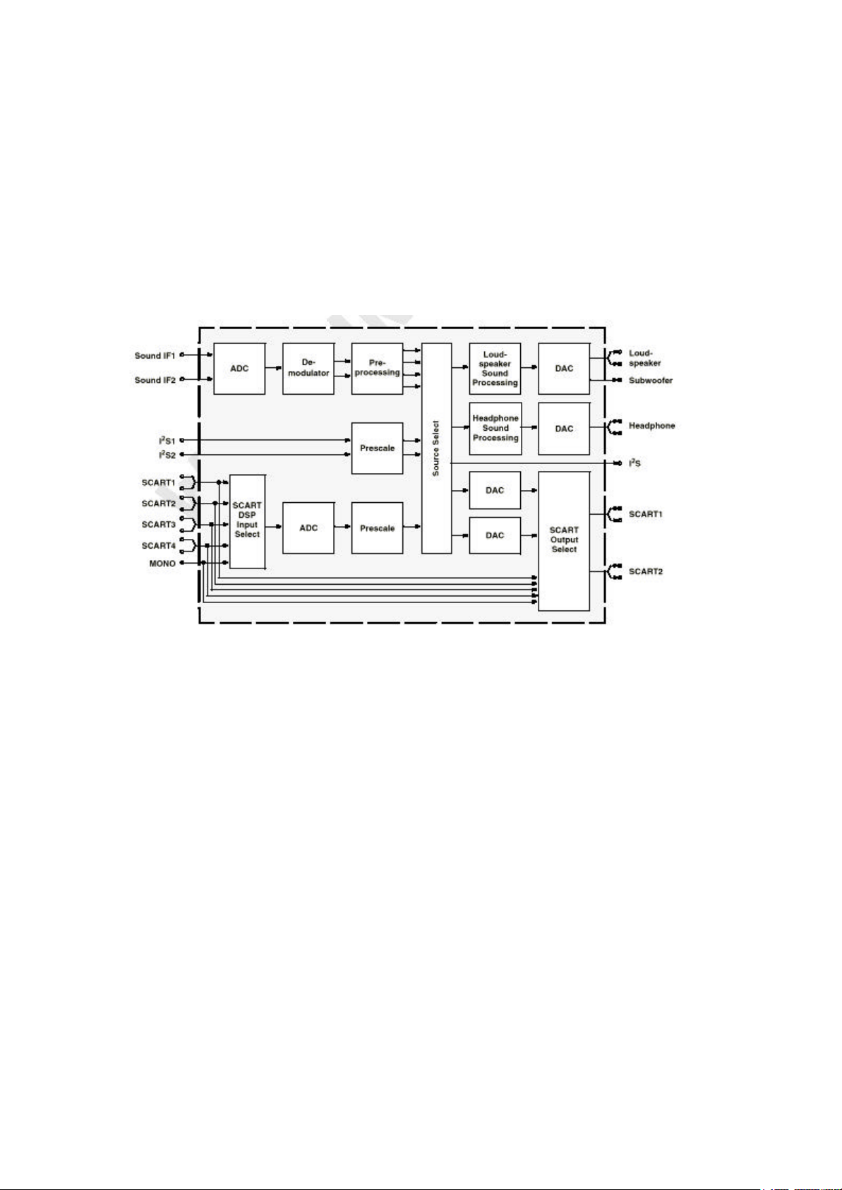
“PANORAMA” algorithm. These TV sound processing ICs include versions for processing the multichannel television sound (MTS) signal conforming to the standard recommended by the Broadcast
Television Systems Committee (BTSC). The DBX noise reduction, or alternatively, Micronas Noise
Reduction (MNR) is performed alignment free. Other processed standards are the Japanese FM -FM
multiplex standard (EIA-J) and the FM Stereo Radio standard. Current ICs have to perform adjustment
procedures in order to achieve good stereo separation for BTSC and EIA-J. The MSP34x1G has
optimum stereo performance without any adjustments. All MSP 34xxG versions are pin and software
downward compatible to the MSP 34xxD. MSP34x1G further simplifies controlling software. Standard
selection requires a singleI2C transmission only. The MSP34x1G has built-in automatic functions: The
IC is able to detect the actual sound standard automatically (Automatic Standard Detection).
Furthermore, pilot levels and identification signals can be evaluated internally with subsequent
switching between mono/stereo/bilingual; no I2C interaction is necessary (Automatic Sound Selection).
14.13.2.Features
3D-PANORAMA virtualizer (approved by Dolby Laboratories) with noise generator
PANORAMA virtualizer algorithm
Standard Selection with single I2C transmission
Automatic Standard Detection of terrestrial TV standards/Automatic Carrier Mute function
Automatic Sound Selection (mono/stereo/bilingual), new registers MODUS, STATUS
Two selectable sound IF (SIF) inputs
Interrupt output programmable (indicating status change)
Loudspeaker / Headphone channel with volume, balance, bass, treble, loudness
Loudspeaker channel with MDB (Micronas Dynamic Bass)
AVC: Automatic Volume Correction
Subwoofer output with programmable low -pass and complementary high-pass filter
5-band graphic equalizer for loudspeaker channel
Spatial effect for loudspeaker channel; processing of all deemphasis filtering
Four Stereo SCART (line) inputs, one Mono input; two Stereo SCART outputs
Complete SCART in/out switching matrix
Two I2S inputs; one I2S output
All analog FM-Stereo A2 and satellite standards
All analog Mono sound carriers including AM-SECAM L
Simultaneous demodulation of (very) high -deviation FM-Mono and NICAM
Adaptive deemphasis for satellite (Wegener-Panda, acc. to ASTRA specification)
ASTRA Digital Radio (ADR) together with DRP 3510A
All NICAM standards
Korean FM-Stereo A2 standard
19
14.13.3.Pin connections
NC = not connected; leave vacant
LV = if not used, leave vacant
X = obligatory; connect as described in circuit diagram
DVSS: if not used, connect to DVSS
AHVSS: connect to AHVSS
Pin No. Pin Name Type
PLCC
68-pin
1 16 14 9 8 ADR_WS OUT LV ADR word strobe
2 - - - - NC LV Not connected
3 15 13 8 7 ADR_DA OUT LV ADR Data Output
4 14 12 7 6 I2S_DA_IN1 IN LV I2S1 data input
5 13 11 6 5 I2S_DA_OUT OUT LV I2S data output
6 12 10 5 4 I2S_WS IN/OUT LV I2S word strobe
7 11 9 4 3 I2S_CL IN/OUT LV I2S clock
8 10 8 3 2 I2C_DA IN/OUT X I2C data
9 9 7 2 1 I2C_CL IN/OUT X I2C data
10 8 - 1 64 NC LV Not connected
11 7 6 80 63 STANDBYQ IN X Stand-by (low-active)
12 6 5 79 62 ADR_SEL IN X I2C bus address select
13 5 4 78 61 D_CTR_I/O_0 IN/OUT LV D_CTR_I/O_0
14 4 3 77 60 D_CTR_I/O_1 IN/OUT LV D_CTR_I/O_1
15 3 - 76 59 NC LV Not connected
16 2 - 75 58 NC LV Not connected
17 - - - - NC LV Not connected
18 1 2 74 57 AUD_CL_OUT OUT LV
19 64 1 73 56 TP LV Test pin
20 63 52 72 55 XTAL_OUT OUT X Crystal oscillator
21 62 51 71 54 XTAL_IN IN X Crystal oscillator
22 61 50 70 53 TESTEN IN X Test pin
23 60 49 69 52 ANA_IN2+ IN
24 59 48 68 51 ANA_IN- IN
25 58 47 67 50 ANA_IN1+ IN LV IF input 2
26 57 46 66 49 AVSUP X Analog power supply 5v
- - - 65 - AVSUP X Analog power supply 5v
- - - 64 - NC LV Not connected
- - - 63 48 NC LV Not connected
27 56 45 62 48 AVSS X Analog ground
- - - 61 - AVSS X Analog ground
28 55 44 60 47 MONO_IN IN LV Mono input
- - - 59 - NC LV Not connected
29 54 43 58 46 VREFTOP X
30 53 42 57 45 SC1_IN_R IN LV SCART 1 input, right
31 52 41 56 44 SC1_IN_L IN LV SCART 1 input, left
32 51 - 55 43 ASG AHVSS Analog Shield Ground
33 50 40 54 42 SC2_IN_R IN LV SCART 2 input, right
34 49 39 53 41 SC2_IN_L IN LV SCART 2 input, left
35 48 - 52 40 ASG AHVSS Analog Shield Ground
36 47 38 51 39 SC3_IN_R IN LV SCART 3 input, right
37 46 37 50 38 SC3_IN_L IN LV SCART 3 input, left
38 45 - 49 37 ASG AHVSS Analog Shield Ground
39 44 - 48 36 SC4_IN_R IN LV SCART 4 input, right
40 43 - 47 35 SC4_IN_L IN LV SCART 4 input, left
41 - - 46 - NC LV or AHVSS Not connected
42 42 36 45 34 AGNDC X Analog reference voltage
43 41 35 44 33 AHVSS X Analog ground
- - - 43 - AHVSS X Analog ground
- - - 42 - NC LV Not connected
- - - 41 - NC LV Not connected
44 40 34 40 32 CAPL_M X Volume capacitor MAIN
45 39 33 39 31 AHVSUP X Analog power supply 8V
PSDIP
64-pin
PSDIP
52-pin
PQFP
80-pin
PLQFP
64-pin
Connection
(if not used)
AVSS via 56
pF/LV
AVSS via 56
pF/LV
Short Description
Audio clock output
(18.432 MHz)
IF Input 2 (can be left
vacant, only if IF input 1 is
also not in use)
IF common (can be left
vacant, only if IF input 1 is
also not in use)
Reference voltage IF A/D
converter
20
46 38 32 38 30 CAPL_A X Volume capacitor AUX
47 37 31 37 29 SC1_OUT_L OUT LV SCART output 1, left
48 36 30 36 28 SC1_OUT_R OUT LV SCART output 1, right
49 35 29 35 27 VREF X Reference ground 1
50 34 28 34 26 SC2_OUT_L OUT LV SCART output 2, left
51 33 27 33 25 SC2_OUT_R OUT LV SCART output 2, right
52 - - 32 - NC LV Not connected
53 32 - 31 24 NC LV Not connected
54 31 26 30 23 DACM_SUB OUT LV Subwoofer output
55 30 - 29 22 NC LV Not connected
56 29 25 28 21 DACM_L OUT LV Loudspeaker out, left
57 28 24 27 20 DACM_R OUT LV Loudspeaker out, right
58 27 23 26 19 VREF2 X Reference ground 2
59 26 22 25 18 DACA_L OUT LV Headphone out, left
60 25 21 24 17 DACA_R OUT LV Headphone out, right
- - - 23 - NC LV Not connected
- - - 22 - NC LV Not connected
61 24 20 21 16 RESETQ IN X Power-on-reset
62 23 - 20 15 NC LV Not connected
63 22 - 19 14 NC LV Not connected
64 21 19 18 13 NC LV Not connected
65 20 18 17 12 I2S_DA_IN2 IN LV I2S2-data input
66 19 17 16 11 DVSS X Digital ground
- - - 15 - DVSS X Digital ground
- - - 14 - DVSS X Digital ground
67 18 16 13 10 DVSUP X Digital power supply 5V
- - - 12 - DVSUP X Digital power supply 5V
- - - 11 - DVSUP X Digital power supply 5V
68 17 15 10 9 ADR_CL OUT LV ADR clock
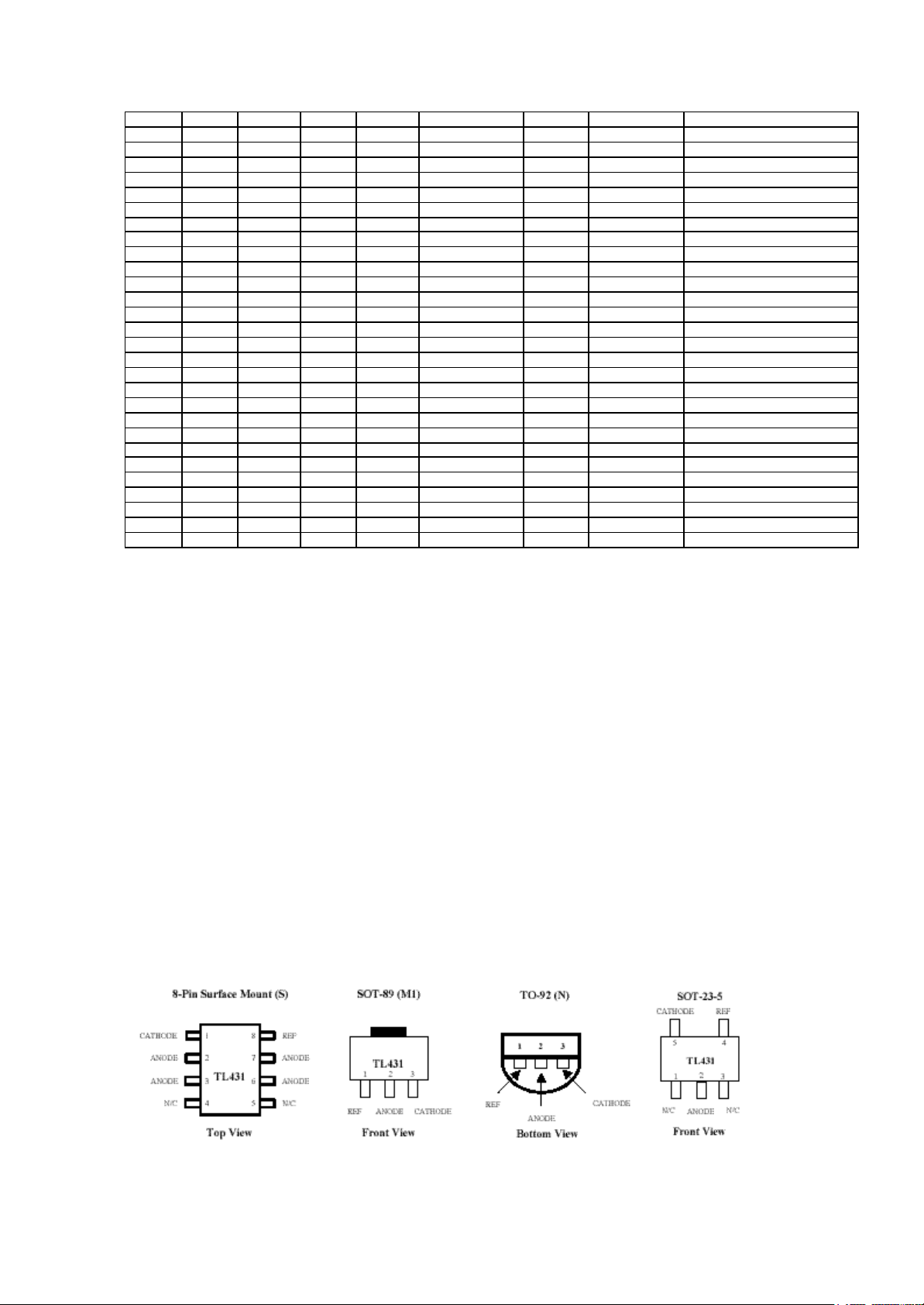
14.14.TL431
14.14.1.Description
The TL431 is a 3-terminal adjustable shunt voltage regulator providing a highly accurate 1 % band gap
reference. TL431 acts as an open-loop error amplifier with a 2.5V temperature compensation reference.
The TL431 thermal stability, wide operating current (150mA) and temperature range (0.to 105.makes it
suitable for all variety of application that are looking for a low cost solution with high performance. The
output voltage may be adjusted to any value between VREF and 36 volts with two external resistors.
The TL431 is operating in full industrial temperature range of 0°C to 105°C. The TL431 is available in
TO-92, SO-8, SOT-89 and SOT23 -5 packages.
14.14.2.Features
• Trimmed Band gap to 1%
• Wide Operating Current 1mA to 150mA
• Extended Temperature Range 0. °C to 105.°C
• Low Temperature Coefficient 30 ppm /°C
• Offered in TO-92, SOIC, SOT-89, SOT-23-5
• Improved Replacement in Performance for TL431
• Low Cost Solution
14.14.3.Pin Configurations
21

14.15.DRX3960A
14.15.1.Introduction
The Digital Receiver Front-end DRX 3960A perfo rms the entire multi-standard Quasi Split Sound (QSS)
TV IF processing, AGC, video demodulation, and generation of the second sound IF (SIF) with only one
SAW filter. The IC is designed for applications in TV sets, VCRs, PC cards, and TV tuners. The
alignment-free DRX 3960A needs no special external components. All control functions and status
registers are accessible via I2C bus interface. Therefore, it simplifies the design of high -quality, highly
standardized IF stages. Due to its mixed signal structure and the digital demodulation, the IC offers
unique features and is prepared for digital TV.
14.15.2.Features
– Multi-standard QSS IF processing with a single SAW
– Highly reduced amount of external components (no tank circuit, no potentiometers, no SAW
switching)
– Programmable IF frequency (38.9 MHz, 45.75 MHz, 32.9 MHz, 36.125 MHz etc.)
– Digital IF processing for the following standards: B/G, D/K, I, L/L’, and M/N
– Standard specific digital post filtering
– Standard specific digital video/audio splitting
– Standard specific digital picture carrier recovery:
– alignment -free
– Quartz-stable and accurate
– Stable frequency lock at 100% modulation and over modulation up to 115%
– Quartz-accurate AFC information
– Programmable standard specific digital group delay equalizing
– Automatically frequency-adjusted Nyquist slope, therefore optimal picture and sound performance
over complete lock in frequency range
– Standard specific digital AGC and delayed tuner AGC with programmable tuner Take Over Point
– Fast AGC due to linear structure
– Adaptive back porch control, therefore fast positive modulation AGC
– No sound traps needed at video output
– Second SIF output with standard dependent pre -filtering and amplitude controlled output level
– Optimal sound SNR due to carrier recovery without quadrature distortions
– FM radio capability without external components and with standard TV tuner
– Prepared for digital TV (DVB -C, DVB-T, ATSC)
2
– I
C bus interface
14.15.3.Pin connection and short descriptions
NC = not connected, leave vacant LV = if not used, leave vacant
DVSS = if not used, connect to DVSS AHVSS = connect to AHVSS
X = obligatory; connect as described in circuit diagram
Pin no
PLCCK 68 pin
1 AVSS_ADC
2 AVDD_ADC
3 ANASTX I/O AVDD_FE8 GND Test pin
4 ANASTY I/O AVDD_FE8 GND Test pin
5 AVDD_FE8 X 2nd analog supply for the front -end
6 AVSS_FE8 X 2nd analog ground for the front -end
7 AVSS_FE40 1st analog ground for the front -end
8 IFINX IN AVDD_FE40 X IF Input
9 AVDD_FE40 X 1st analog supply for the front -end
10 IFINY IN AVDD_FE40 X IF Input
11 AVSS_FE40 X 1st analog ground for the front -end
12 AVDD_SYN X Analog supply for synthesizer (+5V)
13 AVSS_SYN X Analog ground for synthesizer
14 SHIELD IN X Shield GND
15 TEST0 IN AVDD_DAC GND Test pin
16 TEST1 IN AVDD_DAC GND Test pin
17 TEST2 IN AVDD_DAC GND Test pin
Pin name Type
Supply
Voltage
Connection
(if not used)
X Analog Ground for ADC
X Analog Supply for ADC (+5V)
Short description
22
18 CVBS OUT AVDD_DAC X CVBS Output
19 REF_SW IN AVDD_DAC X Reference frequency switch
20 SIF OUT AVDD_DAC X 2nd SIF output
21 AVDD_DAC X DAC supply (+5V)
22 AVSS_DAC X DAC ground
23 TEST_EN IN DVDD GND Test enable
24 RESETQ IN DVDD X Reset
25 I2C_SDC I/O DVDD X I2C data
26 I2C_SCL I/O DVDD X I2C clock
27 DVDD_CAP X Digital supply capacitor
28 DVDD X Digital supply (+3.3V)
29 DVSS X Digital ground
30 DVSS_CAP X Digital capacitor ground
31 PORT0 OUT DVDD LV Digital output port
32 PORT1 OUT DVDD LV Digital output port
33 TUNER_AGC OUT DVDD X Tuner AGC current output
34 PORT2 OUT DVDD LV Digital output port
35 PORT3 OUT DVDD LV Digital output port
36 PORT4 OUT DVDD LV Digital output port
37 ADR_SEL IN DVDD X Address select
38 PORT5 OUT DVDD LV Digital output port
39 DVDD_ADC X Digital supply for ADC (+3.3V)
40 DVSS_ADC X Digital ground for ADC
41 XTAL_IN IN AVDD_ADC X Crystal oscillator
42 XTAL_OUT I/O AVDD_ADC X Crystal oscillator/external reference
frequency
43 VREF AVDD_ADC X ADC Reference voltage
44 SGND AVDD_ADC X ADC Reference ground
14.16.LM7808
14.16.1.Description
The L7800 series of three -terminal positive regulators is available in TO -220 TO -220FP TO-3 and D 2
PAK packages and several fixed output voltages, making it useful in a wide range of applications.
These regulators can provide local on-card regulation, eliminating the distribution problems associated
with single point regulation. Each type employs internal current limiting, thermal shutdown and safe
area protection, making it essentially indestructible. If adequate heat sinking is provided, they can
deliver over 1A output current. Although designed primarily as fixed voltage regulators, these devices
can be used with external components to obtain adjustable voltages and currents.
14.16.2.Features
Output Current Up To 1.5 A
Output Voltages of 5; 5.2; 6; 8; 8.5; 9; 12; 15; 18; 24V
Thermal Over load protection
Short Circuit Protection
Output Transition SOA Protection
14.17.BDX53BFI
14.17.1.Description
The BDX53BFI is silicon epitaxial-base NPN power transistor in monolithic Darlington configuration and
are mounted in ISOWATT220 plastic package. It is intended for use in hammer drivers, audio amplifiers
and other medium power linear and switching applications. The complementary PNP type is the
BDX54BFI.
14.17.2.Applications
General purpose switching and amplifier
Linear and switching industrial equipment
23
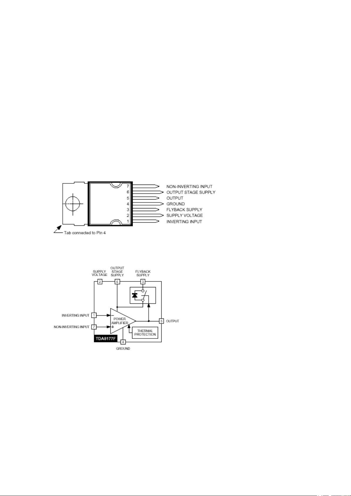
14.18.TDA8177F
14.18.1.Description
Designed for monitors and high performance TVs, the TDA8177F vertical deflection booster can handle
flyback voltage up to 70V. More than this it is possible to have a flyback voltage, which is more than the
double of the supply (Pin 2). This allows to decrease the power consumption or to decrease the flyback
time for a given supply voltage. The TDA8177F operates with supplies up to 35V and provides up to
3APP output current to drive the yoke.
14.18.2.Features
Power Amplifier
Thermal Protection
Output Current Up To 3.0APP
Flyback Voltage Up To 70V (on Pin 5)
Suitable For Dc Coupling Application
External Flybac k Supply
14.18.3.Pin connections
14.18.4.Block Diagram
14.19.LM1086
14.19.1.Description
The LM1086 is a series of low dropout positive voltage regulators with a maximum dropout of 1.5V at
1.5A of load current. It has the same pin-out as National Semiconductor’s industry standard LM317.
The LM1086 is available in an adjustable version, which can set the output voltage with only two
external resistors. It is also available in five fixed voltages: 2.5V, 2.85V, 3.3V, 3.45V and 5.0V. The fixed
versions integrate the adjust resistors. The LM1086 circuit includes a zener trimmed band-gap
reference, current limiting and thermal shutdown.
14.19.2.Features
Available in 2.5V, 2.85V, 3.3V, 3.45V, 5V and Adjustable Versions
Current Limiting and Thermal Protection
24

Output Current 1.5A
Line Regulation 0.015% (typical)
Load Regulation 0.1% (typical)
14.19.3.Applications
SCSI-2 Active Terminator
High Efficiency Linear Regulators
Battery Charger
Post Regulation for Switching Supplies
Constant Current Regulator
Microprocessor Supply
14.19.4.Connection Diagrams
14.20.MC44608
14.20.1.Description
The MC44608 is a high performance voltage mode controller designed for off–line converters. This high
voltage circuit that integrates the start–up current source and the oscillator capacitor, requires few
external components while offering a high flexibility and reliability. The device also features a very high
efficiency stand–by management consisting of an effective Pulsed Mode operation. This technique
enables the reduction of the stand–by power consumption to approximately 1W while delivering 300mW
in a 150W SMPS.
• Integrated Start –Up Current Source
• Lossless Off–Line Start –Up
• Direct Off–Line Operation
• Fast Start –Up
14.20.2.General Features
• Flexibility
• Duty Cycle Control
• Under voltage Lockout with Hysteresis
• On Chip Oscillator Switching Frequency 40, or 75kHz
• Secondary Control with Few External Components
Protections
• Maximum Duty Cycle Limitation
• Cycle by Cycle Current Limitation
• Demagnetization (Zero Current Detection) Protection
• “Over VCC Protection” Against Open Loop
• Programmable Low Inertia Over Voltage Protection Against Open Loop
• Internal Thermal Protection
GreenLineTM Controller
• Pulsed Mode Techniques for a Very High Efficiency Low Power Mode
• Lossless Startup
• Low dV/dT for Low EMI Radiations
25
 Loading...