

Page 1

FILE NO. 030-200503
SERVICE MANUAL
LCD Color Television
27WL56P
TOSHIBA CORPORATION, 2005
Published in Japan, Apr. 2005 (YC)
Page 2

TABLE OF CONTENTS
SERVICE SAFETY PRECAUTIONS .................................................................................................................................... 3
HANDLING THE LCD MODULE .......................................................................................................................................... 5
SERVICE MODE .................................................................................................................................................................. 7
LOCATION OF CONTROLS ............................................................................................................................................... 12
LAYOUT OF MAJOR BOARDS .......................................................................................................................................... 14
MECHANICAL DISASSEMBLY .......................................................................................................................................... 15
EXPLODED VIEW .............................................................................................................................................................. 17
PACKING DISASSEMBLY ................................................................................................................................................. 19
CHASSIS AND CABINET REPLACEMENT PARTS LIST ................................................................................................. 20
PC BOARDS TOP & BOTTOM VIEW ................................................................................................................................ 26
CIRCUIT BLOCK DIAGRAM .............................................................................................................................................. 40
SPECIFICATIONS ............................................................................................................................................................. 41
APPENDIX:
SCHEMATIC DIAGRAM
-
2
-
Page 3
GENERAL ADJUSTMENTS
SPECIFIC INFORMATIONS
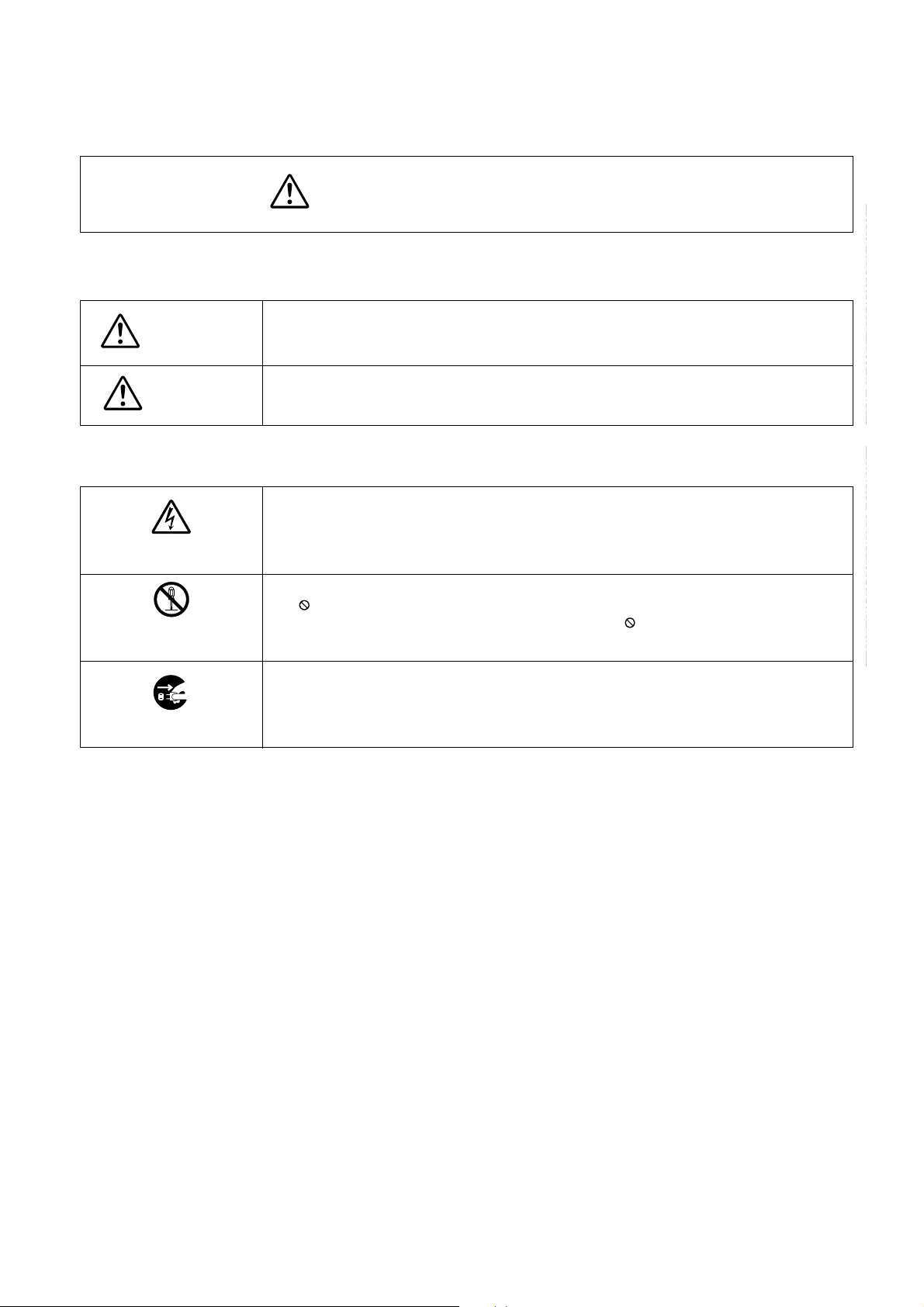
SERVICE SAFETY PRECAUTIONS
• The caution items shown here describe major safety issues and should always be observed.
• The meanings of the various indications are as follows.
WARNING
CAUTION
* Physical damage means major damage to a home, furnishings and other possessions.
Examples of marks
SHOCK HAZARD
PROHIBIT DISASSEM-
BLING
UNPULUG
Indicates a hypothetical situation in which service personnel and nearby third parties, or even
end users due to a product defect after the service operation is completed, could possibly be in
danger of injury or even death in the event of operational error.
Indicates a hypothetical situation in which service personnel and nearby third parties, or even
end users after the service operation is completed, could possibly be in danger of injury, or
where there could be physical damage in the event of operational error.
The" indicates caution (including danger and warning).
The actual meaning of this caution is indicated inside the
The example shown to the left indicates the danger of "electrical shock".
indicates a forbidden action.
The
The actual meaning of this caution is indicated inside the
The example shown to the left indicates that disassembly is forbidden.
The
-
indicates a forced action (an action that must be performed).
The actual meaning of this forced action is indicated by
The example shown to the left indicates that the power plug must be disconnected.
"
or nearby illustrations or text.
or nearby illustrations or text.
-
or nearby illustrations or text.
-
3
-
Page 4
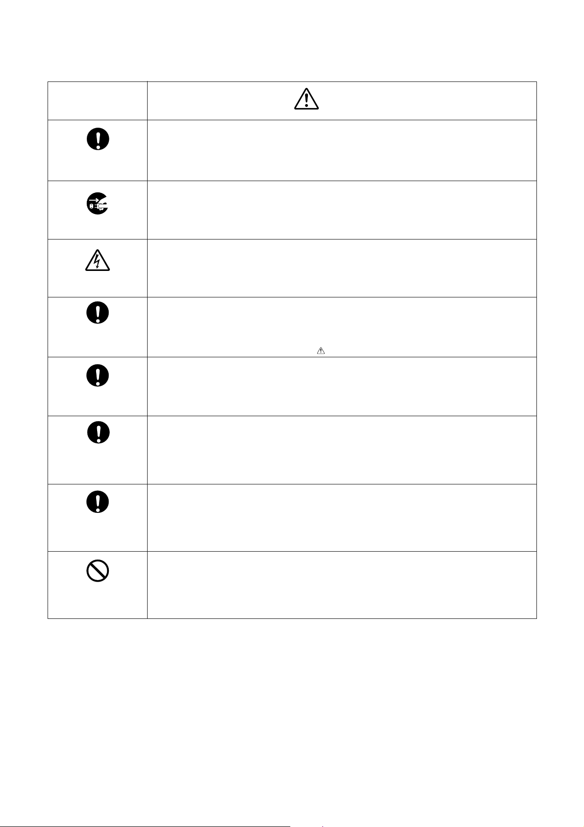
KEEP CHILDREN
AWAY
UNPULUG
SHOCK HAZARD
USE SPECIFIED
PARTS
CAUTION FOR
WIRING
CAUTION FOR
ASSEMBLING /
WIRING
WARNING
• Always advise users to keep children away.
There is danger of injury to children from tools, disassembled products, etc.
• Always disconnect the power plug before starting work whenever power is not required.
Failure to disconnect the power plug before starting work can result in electrical shock.
• Depending on the model, use an insulation transformer or wear gloves when servicing with the
power on, and disconnect the power plug to avoid electrical shock when replacing parts.
In some cases, alternating current is also impressed in the chassis, so electrical shock is possible if the chassis is contacted with the power on.
• Always use the replacement parts specified for the particular model when making repairs.
The parts used in products have the necessary safety characteristics such as inflammability,
voltage resistance, etc.; therefore, use only replacement parts that have these same characteristics.
Use only the specified parts when the
• Parts mounting and routing of the wiring should be the same as that used originally.
For safety purposes, insulating materials such as tubing or tape is sometimes used and printed
circuit boards are sometimes mounted floating.
Also make sure that wiring is routed and clamped to avoid parts that generate heat and which
use high voltage. Always follow the original scheme.
• After a repair has been completed, reassemble all disassembled parts, and route and reconnect the wiring, in accordance with the original scheme.
Do not allow internal wiring to be pinched by cabinets, panels, etc.
Any error in reassembly or wiring can result in electrical leakage, flame, etc., and may be
hazardous.
mark is included in a circuit diagram or parts list.
CHECK INSULATION
RESISTANCE
PROHIBIT
REMODELING
• After completing the work, disconnect the power plug from the outlet, remove the antenna, turn
on the power switch. Then, use a 500V insulation resistance meter to check the insulation
resistance of the antenna terminal, other metallic parts and between the prongs of the power
plug to make sure that the insulation resistance is 1M 1 or more.
The set will require inspection and repair if the insulation resistance is below this value.
• Never remodel the product in any way.
Remodeling can result in improper operation, malfunction, or electrical leakage and flame,
which may be hazardous
-
4
-
Page 5
GENERAL ADJUSTMENTSSPECIFIC INFORMATIONS
HANDLING THE LCD MODULE
Safety Precautions
In the event that the screen is damaged or the liquid crystal
(fluid) leaks, do not breathe in or drink this fluid. Also, never
touch this fluid.
Such actions could cause toxicity or skin irritation. If this fluid
should enter the mouth, rinse the mouth thoroughly with water. If the fluid should contact the skin or clothing, wipe off
with alcohol, etc., and rinse thoroughly with water. If the fluid
should enter the eyes, immediately rinse the eyes thoroughly
with running water.
Precautions for Handling the LCD Module
The LCD module can easily be damaged during disassembly
or reassembly; therefore, always observe the following precautions when handling the module.
1. When attaching the LCD module to the LCD cover, position it appropriately and fasten at the position where the
display can be viewed most conveniently.
3. If the panel surface becomes soiled, wipe with cotton or a
soft cloth. If this does not remove the soiling, breathe on
the surface and then wipe again.
If the panel surface is extremely solied, use a CRT cleaner
as a cleaner. Wipe off the panel surface by drop the cleaner
on the cloth. Do not drop the cleaner on the panel. Pay
attention not to scratch the panel surface.
4. Leaving water or other fluids on the panel screen for an
extended period of time can result in discoloration or
stripes. Immediately remove any type of fluid from the
screen.
2. Carefully align the holes at all four corners of the LCD
module with the corresponding holes in the LCD cover
and fasten with screws. Do not strongly push on the module because any impact can adversely affect the performance. Also use caution when handling the polarized screen
because it can easily be damaged.
The metal edges of the LCD module
CAUTION
are sharp, so use caution to avoid injury.
5. Glass is used in the panel, so do not drop or strike with
hard objects. Such actions can damage the panel.
6. CMOS-LSI circuitry is used in the LCD module, so avoid
damage due to static electricity. When handling the module, use a wrist ground or anchor ground.
-
5
-
Page 6
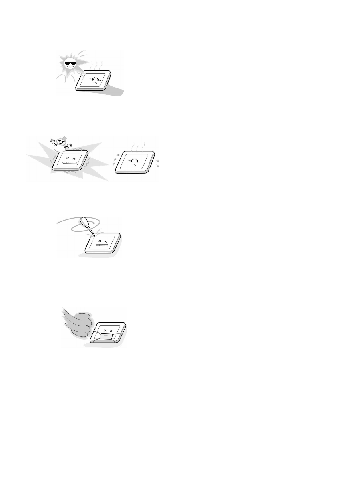
7. Do not expose the LCD module to direct sunlight or strong
ultraviolet rays for an extended period of time.
8. Do not store the LCD module below the temperature conditions described in the specifications. Failure to do so
could result in freezing of the liquid crystal due to cold air
or loss of resilience or other damage.
9. Do not disassemble the LCD module. Such actions could
result in improper operation.
10. When transporting the LCD module, do not use packing
containing epoxy resin (amine) or silicon resin (alcohol or
oxim). The gas generated by these materials can cause
loss of polarity.
-
6
-
Page 7
SERVICE MODE
1. ENTERING SERVICE MODE
1) Press
Remote Control. keep pressing. press MENU button on TV set.
2. DISPLAYING THE ADJUSTMENT MENU
1) Press MENU button on TV.
3. KEY FUNCTION IN THE SERVICE MODE
The following key entry during display of adjustment menu provides special functions.
button once on 2) Press button again and 3) While pressing the button,
or Sound Mute
Service mode Adjustment mode
Press
Press
(Service mode display)
Test signal selection : a button (on Remote)
Selection of the adjustment items : Channel s/t (on TV or Remote)
Change of the data value : Volume ; +/– (on TV or Remote)
Adjustment menu mode ON/OFF : MENU button (on TV)
Initialization of the memory : CALL + Channel button on TV (s)
Reset the count of operating protect
circuit to “00”: CALL + Channel button on TV (t)
“RCUT” selection : 1 button
“GCUT” selection : 2 button
“BCUT” selection : 3 button
“SCNT” selection : 4 button
“COLP” selection : 5 button
“TNTC” selection : 6 button
Automatic A/D Adjustment(PC, Component)
Self diagnostic display ON/OFF : 9 button
CAUTION : Never try to perform initialization unless you have changed the memory IC.
: 7 button
Color thickness correction
note: Displayed differently as shown below, de-
pending on the setting of the receiving color
system.
COLP (PAL)
COLC (NTSC)
COLS (SECAM)
-
7
-
Page 8
4. SELECTING THE ADJUSTING ITEMS
1) Every pressing of CHANNEL s button in the service mode changes the adjustment items in the order of table-2.
(t button for reverse order)
5. ADJUSTING THE DATA
1) Pressing of VOLUME ; +/– button will change the value of data in the range from 00H to FFH. The variable range
depends on the adjusting item.
6. EXIT FROM SERVICE MODE
1) Pressing POWER button to turn off the TV once.
■ INITIALIZATION OF MEMORY DATA
After replacing EEPROM IC, the following initialization is required.
1. Enter the service mode, then select any register item.
2. Press and hold the CALL button on the Remote, then press the CHANNEL s button on the TV.The initialization of EEPROM IC
has been complated.
3. Check the picture carefully. If necessary, adjust any adjustment item above.
Perform “Auto tune” on the owner’s manual.
CAUTION: Never attempt to initialize the data unless EEPROM IC has been replaced.
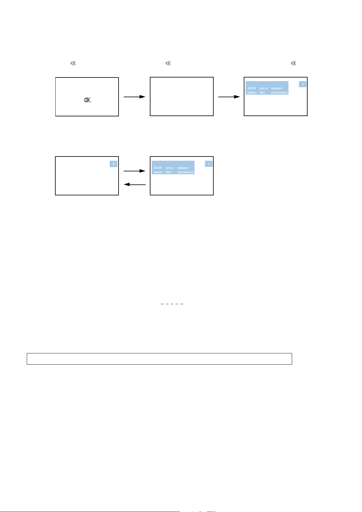
7. TEST SIGNAL SELECTION
1) Every pressing of a button on the Remote Control changes the built-in test patterns on screen as described below
in SERVICE MODE.
R
All BlackAll White
BSignal off G
Signals Picture
• Red raster
• Green raster
• Blue raster
• All Black
• All White
-
8
-
Page 9
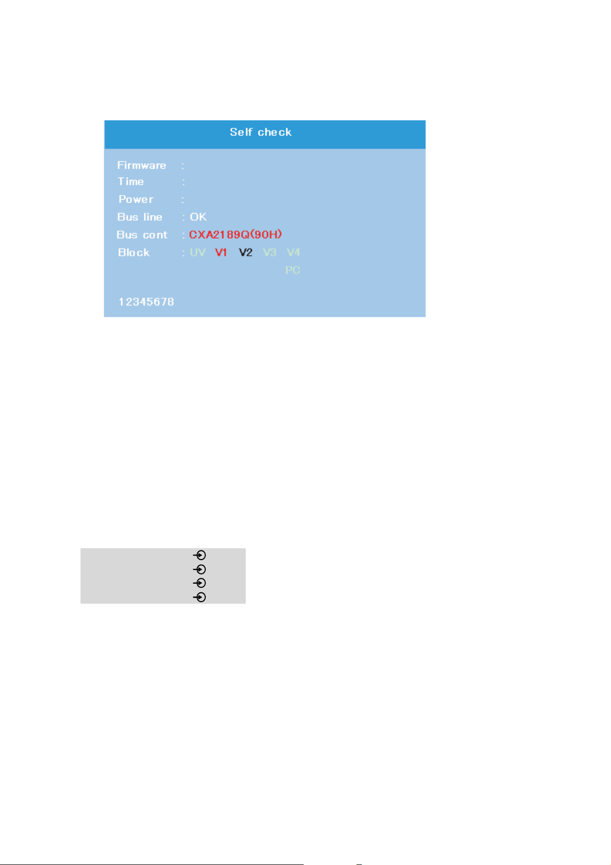
8. SELF DIAGNOSTIC FUNCTION
27WL56P
WL56_EU_0100
1) Press “9” button on Remote Control during display of adjustment menu in the service mode.
The diagnosis will begin to check if interface among IC’s is executed properly.
2) During diagnosis, the following displays are shown.
1
2
3
WL56_EU_0100
000000
000
4
5
6
27WL56P
78
1 Firmware :
Version information of microprocessor
In case of file name : WL56_EU and Version : 0100 indicates[WL56_EU_0100].
2 Time : Total hour of turn the TV on. (Unit : H)
3 Power :Operation number of protecting circuit ----"000" is normal.
When indication is other than "000", overcurrent apt to flow, and circuit parts may possibly be damaged.
4 Bus line : --"OK" is normal
"SCL-GND"(Red indication) : SCL-GND short circuit
"SDA-GND"(Red indication) : SDA-GND short circuit
"SCL-SDA"(Red indication) : SCL-SDA short circuit
5 Bus cont : --- "OK" is normal.
NG is abnormal(Red indication).
When type name of semiconductor indicates.
6 Block
UV : TV reception mode
V1 : VIDEO 1 input mode ( 1)
V2 : VIDEO 2 input mode ( 2)
V3 : VIDEO 3 input mode ( 3)
V4 : VIDEO 4 input mode ( HDMI)
7 8 digit : CD number
8 Model name (7 digit)
-
9
-
Page 10
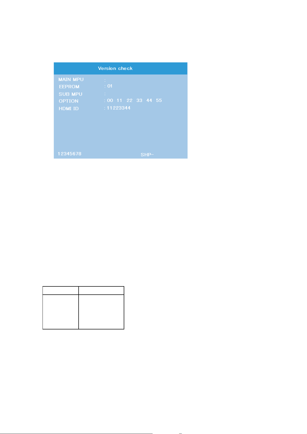
9. VERSION CHECK MODE
1) Press “9” button twice on Remote Control during display of adjustment menu in the service mode. The version of main
MPU will begin to check.
2) During Version Check, the following displays are shown.
1
WL56_EU_0100 (E16)
2
3
2E
4
5
6
27WL56P
27
78
1 MAIN MPU :
Version information of microprocessor
In case of file name : WL56_EU, Version 0100 for Code Program Version
and (E16) for OSD Version indicates [WL56_EU_0100(E16)]
2 EEPROM :
Version information of EEPROM : Display 1 byte data.
3 SUB MPU :
Version information of SUB MPU : Display 1 byte data.
4 OPTION :
Option information : Display six numbers of 1 byte data.
5 HDMI ID :
HDMI ID information : Display 4 byte data.
6 CD number : Display 8 digit number
7 Model name : Display 7 digit number
8 LCD Panel Vender information display
The following Panel Vender and screen size are displayed.
Panel Vender Screen Size(Inch)
LPL -23
SHP -26
CMO -32
-37
-47
Example : SHP-32 indicates that Vender is SHP and Screen Size is 32 inch.
-
10
-
Page 11
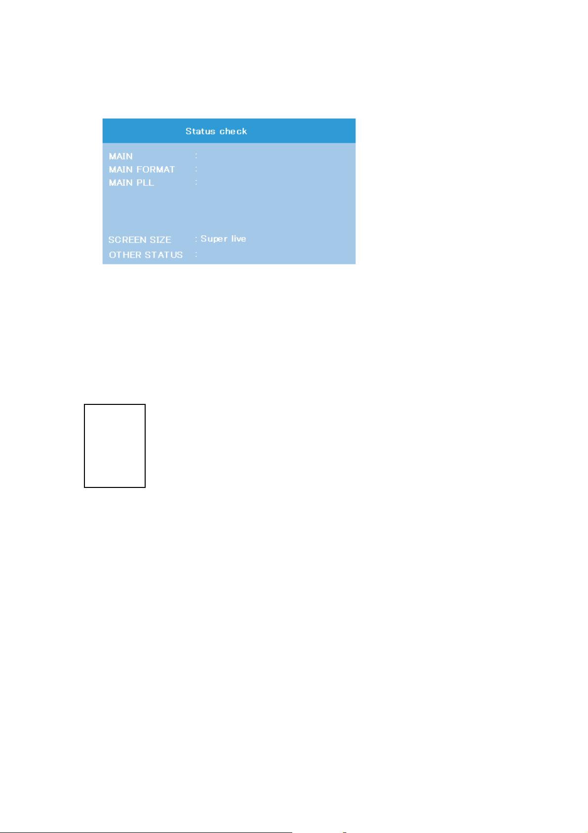
10. STATUS CHECK MODE
1) Press “9” button thrice on Remote Control during display of adjustment menu in the service mode. The status of this model
will begin to check.
2) During Status Check, the following displays are shown.
1
2
3
EXT1
1080i-50
C6 38 54 CE 08
4
5
0000 0000 0000
1 MAIN :
Main source information :
Display RF position number (0 - 99) on the main screen, or Input Source (EXT1/2/3/HDMI etc.)
2 MAIN FORMAT :
Display Video and PC format information
3 MAIN PLL :
Main PLL information : Display 1 byte data at five.
4 SCREEN SIZE :
Display the screen size as follows.
Super live
Cinema
Subtitle
14:9
Wide
4:3
5 OTHER STATUS :
Other status information : Display three numbers of 2 byte data.
-
11
-
Page 12
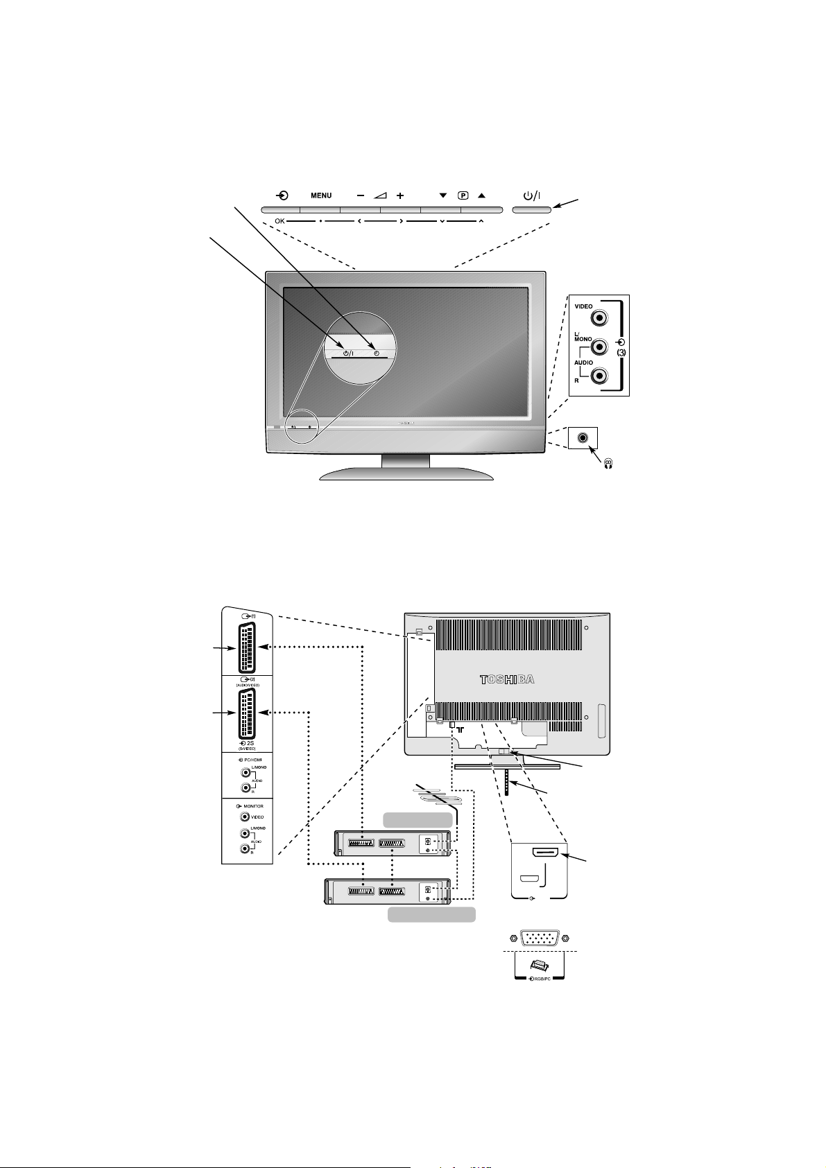
Front
LOCATION OF CONTROLS
Back
GREEN – On-timer set
RED – Power On
Standby
SCART 1 (EXT1)
SCART 2 (EXT2)
TV
IN/OUT
decoder*
MEDIA REC.
SAT
media recorder
CABLE HOLDER
FIXING STRAP
HDMI™ INPUT
HDMI
HDMI
-
12
-
Page 13
Remote control
To bring up on-screen information and
for the text initial/index function
To return to the previous programme
To display text services
For On/Standby mode
Number buttons
To select input from external sources
To access sub-pages when in text mode
Selectable picture preferences
On-screen Menus
Stereo/Bilingual reception
To select mode
When using a TOSHIBA VCR or DVD:
press
to PAUSE
m
press
to EJECT
w
press
to SKIP-REWIND
l
q
press
to SKIP-FORWARD
l
s
press
to PLAY
r
press
to STOP
p
press
to REWIND
q
press
to FAST FORWARD
s
Widescreen viewing
To exit Menus
To change programme positions and
text pages
To alter the volume
When using menus the arrows move the
cursor on the screen up, down, left or
right. OK to confirm your selection
Text control buttons
Bass Boost
To mute the sound
When in TV mode:
Time display
8/9
When in Text mode:
To reveal concealed text
r
To hold a wanted page
q
To enlarge text display size
s
To select a page whilst viewing a
8/9
normal picture
-
13
-
Page 14
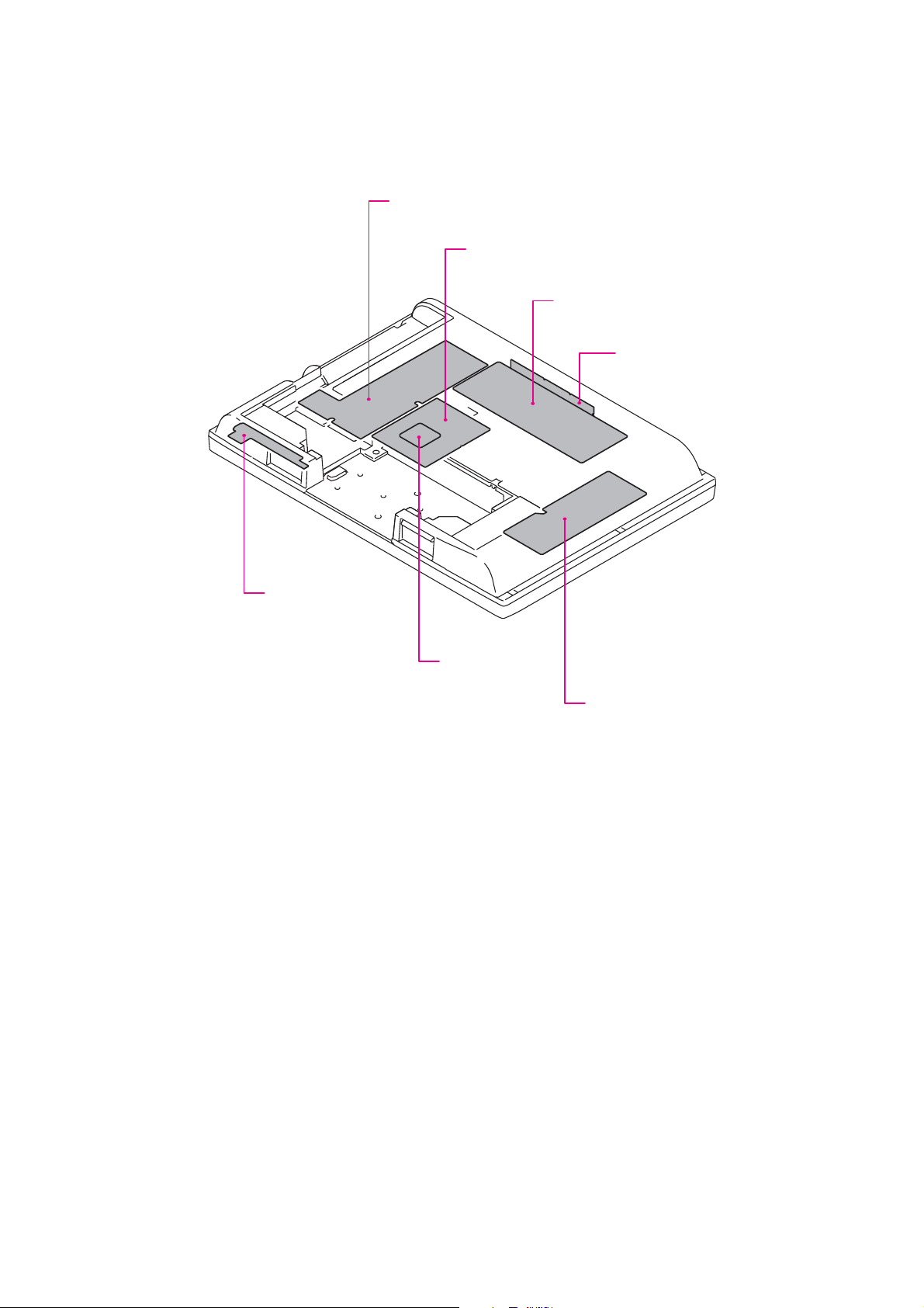
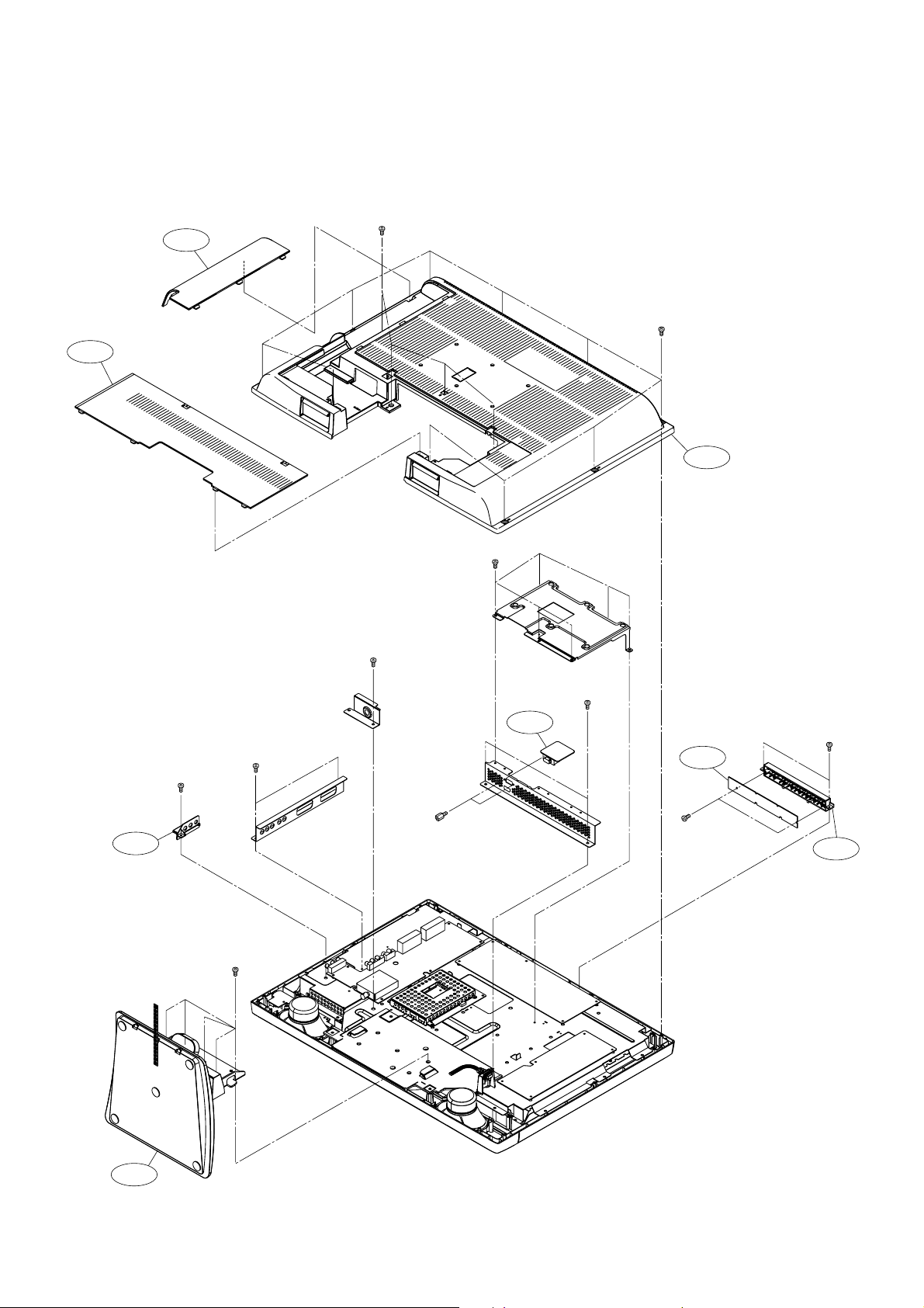
LAYOUT OF MAJOR BOARDS
U004
AV OTHER BOARD
U003
SIGNAL BOARD
U001
POWER BOARD
U006
KEY BOARD
U005
LED/RMT BOARD
U007
PC-IN BOARD
U002
AC-IN BOARD
-
14
-
Page 15
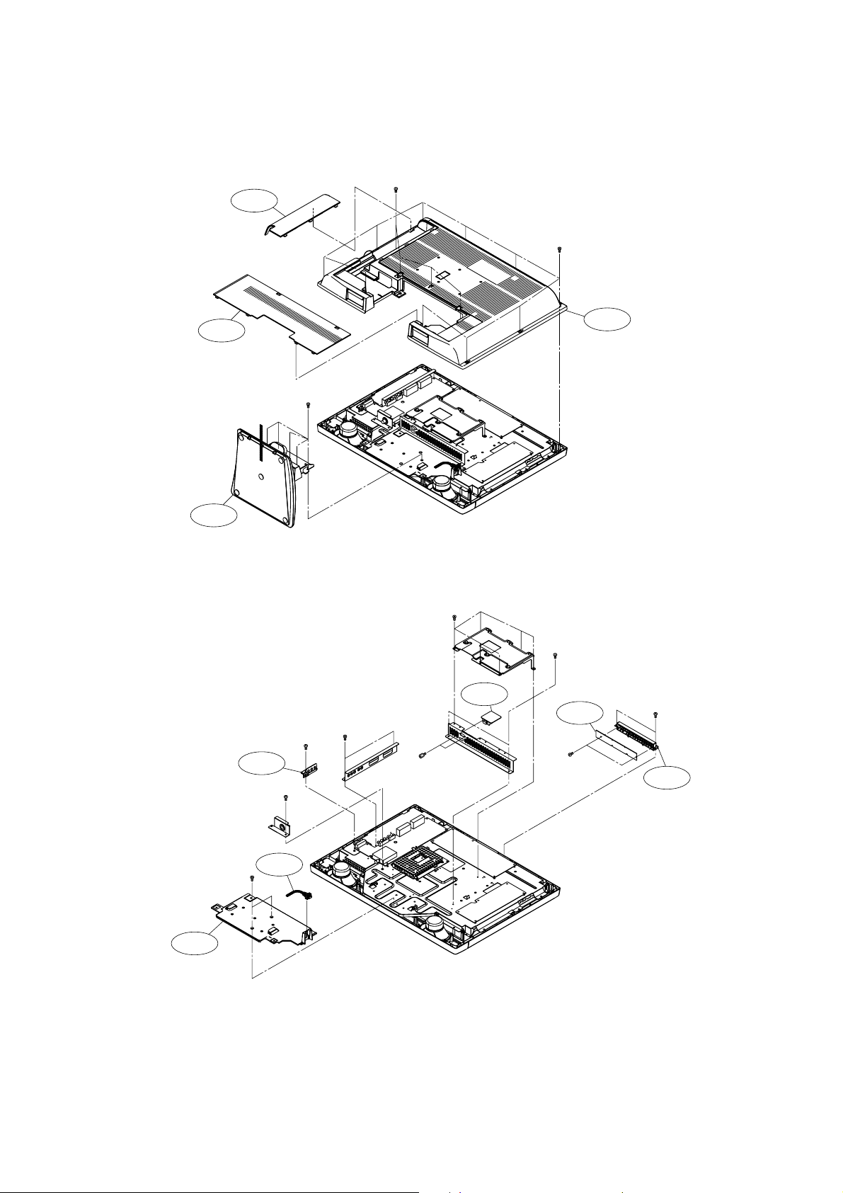
MECHANICAL DISASSEMBLY
1. Remove the stand (foot) and back cover.
A450
PP3×8+SW+W ×4
BITTB3×16 SBN ×10
A445
PP5×16 SW+W SBN
×
3
A420
2. Remove the boards (KEY, PC-IN) and piece key ass'y.
PP4×8+SW+W ×6
PP4×8+SW+W
PP4×8+SW+W
×
2
U007
A401
PP4×8+SW+W ×2
BITTB3×8 SBN
×
U006
2
PP4×8+SW+W
PP3×8+SW+W
×
2
A315
A320
P801
4-40UNC
JFS-4S L=13
-
15
-
BITTB3×12
SBN ×2
A340
Page 16
3. Remove the boards (POWER, AC-IN, SIGNAL, AV OTHER, LED/RMT) and speaker.
PP3×8+SW+W
×
BITTB3×12 SBN
×
2
U005
BITTB4×16 SBN ×4
W661
W661
PP3×8+SW+W
×
4
PP08
BITTB4×16 SBN
×4
H001
U003
PP3×8+SW+W
6
×
5
PP08
U001
U004
PP12
PP3×8+SW+W
×
5
U002
4. Remove the display.
PP4×12+SW+W SBN
×4
PP08
BITTB4×16 SBN
×
14
B001
-
16
A201
-
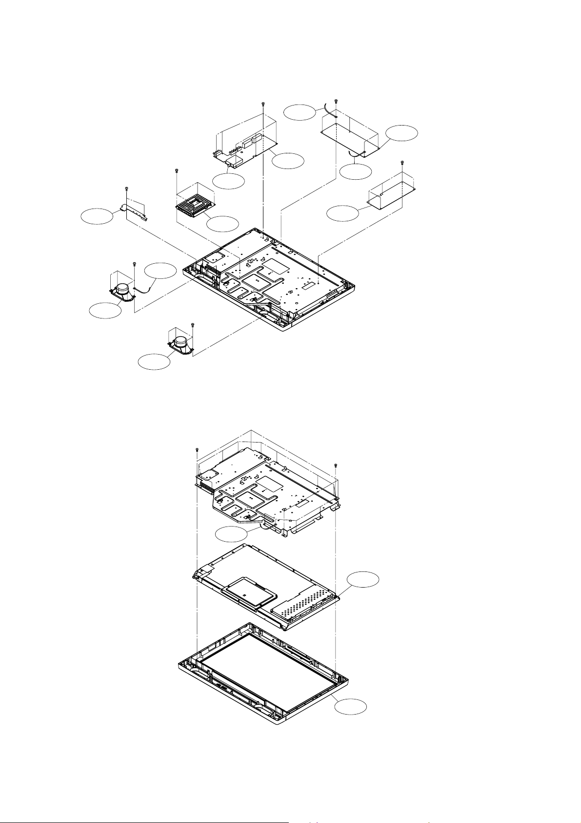
Page 17
1. Chassis Block
A450
A445
EXPLODED VIEWS
PP3×8+SW+W SBN
×
4
BITTB3×16 S B N
×
10
A401
PP4×8+SW+W SBN
A320
PP5×16 SW+W SBN
×
5
PP4×8+SW+W SBN
PP4×8+SW+W SBN
×
2
PP4×8+SW+W SBN
×
6
4-40UNC
JFS-4S L=13
PP4×8+SW+W
×
SBN
U007
2
BITTB3×8 SBN
×
U006
BITTB3×12 SBN
×
2
2
A340
A420
-
17
-
Page 18
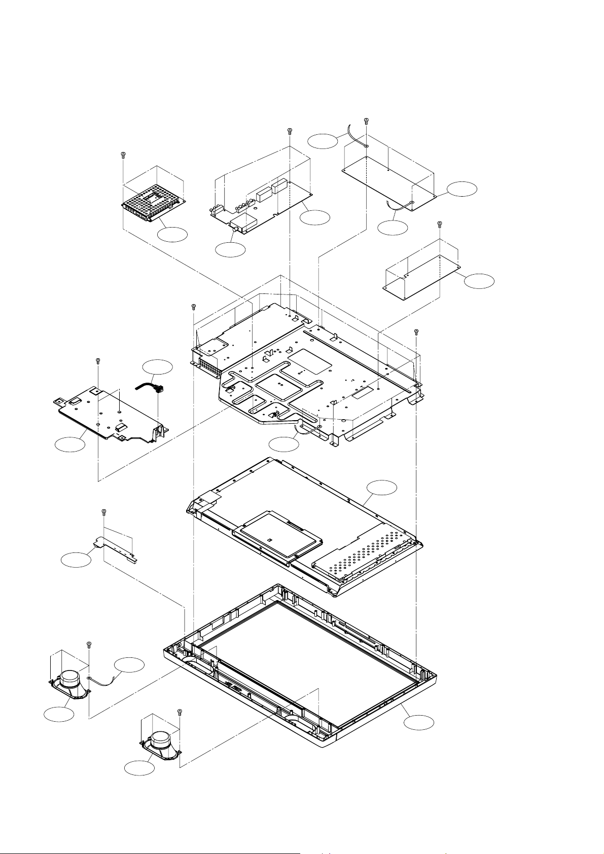
2. Main Block
PP3×8+SW+W SBN
×
PP3×8+SW+W SBN
PP3×8+SW+W SBN
×
6
PP08
4
×
5
U001
PP4×12+SW+W SBN
×
4
PP3×8+SW+W SBN
×
2
A315
BITTB3×12 SBN
×
2
P801
U003
H001
PP08
U004
PP12
B001
PP3×8+SW+W SBN
×
U002
BITTB4×16 SBN
×
14
5
U005
BITTB4×16 SBN
×
4
W661
PP08
BITTB4×16 SBN
×
W661
4
A201
-
18
-
Page 19
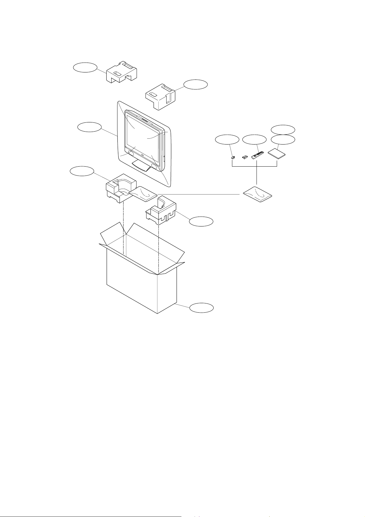
A702A
PACKING DISASSEMBLY
A702A
A703
A702B
Y101
Y130Y170 Y101E
A702B
A701A
-
19
-
Page 20
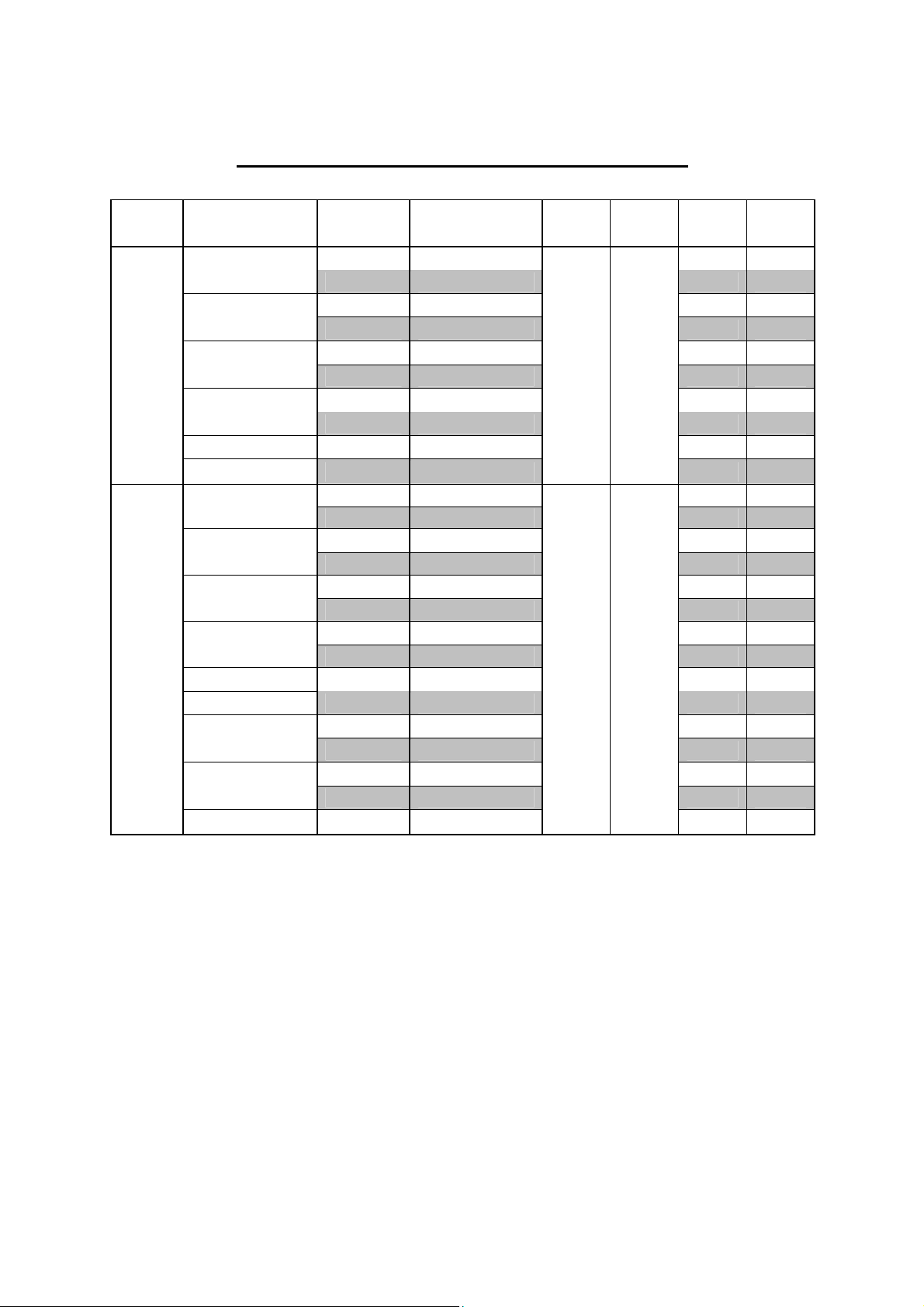
CHASSIS AND CABINET REPLACEMENT PARTS LIST
WARNING: BEFORE SERVICING THIS CHASSIS, READ THE “SERVICE SAFETY PRECAUTIONS” ON PAGE 3 OF
THIS MANUAL.
CAUTION: The international hazard symbols " " in the schematic diagram and the parts list designate com-ponents
which have special characteristics important for safety and should be replaced only with types identical to those in
the original circuit or specified in the parts list. The mounting position of replacements is to be identical with originals.
Before replacing any of these components, read carefully the SERVICE SAFETY PRECAUTIONS. Do not degrade
the safety of the receiver through improper servicing.
NOTICE:
•
The part number must be used when ordering parts, in order to assist in processing, be sure to include the
Model number and Description.
•
The PC board assembly with ∗ mark is no longer available after the end of the production.
Model : 27WL56P
Capacitors ............. CD : Ceramic Disk PF : Plastic Film EL : Electrolytic
Resistors ............... CF : Carbon Film CC : Carbon Composition MF : Metal Film
OMF : Oxide Metal Film VR : Variable Resistor FR : Fusible Resistor
(All CD and PF capacitors are ±5%, 50V and all resistors, ±5%, 1/6W unless otherwise noted.)
Location
No.
Parts No. Description
CAPACITORS
C101 76109103 CERAMIC CHIP, 50V B 0.01UF K
C102 76073019 ELECTROLYTIC, 10V 470UF M 3A
C103 76109102 CERAMIC CHIP, 50V B 1000PF K
C104 76073084 ELECTROLYTIC, 50V 4.7UF M 3A
C105 76073019 ELECTROLYTIC, 10V 470UF M 3A
C162 76105101 CERAMIC CHIP, 50V CH 100PF J
C164 76100103 CERAMIC CHIP, 50V F 0.01UF Z
C190 76092730 CERAMIC CHIP, 16V B 0.1UF K
C501 76092730 CERAMIC CHIP, 16V B 0.1UF K
C502 76092730 CERAMIC CHIP, 16V B 0.1UF K
C503 76794470 ELECTROLYTIC, 16V 47UF M
C504 76109103 CERAMIC CHIP, 50V B 0.01UF K
C505 76794470 ELECTROLYTIC, 16V 47UF M
C506 76109103 CERAMIC CHIP, 50V B 0.01UF K
C514 76763221 ELECTROLYTIC, 16V 220UF M
C516 76105110 CERAMIC CHIP, 50V CH 11PF J
C517 76206478 ELECTROLYTIC, 50V 0.47UF M 7L 3A
C519 76797479 ELECTROLYTIC, 50V 4.7UF M
C521 76092733 CERAMIC CHIP, 50V B 0.022UF K
C524 76109103 CERAMIC CHIP, 50V B 0.01UF K
C526 76109103 CERAMIC CHIP, 50V B 0.01UF K
C527 76797229 ELECTROLYTIC, 50V 2.2UF M
C660 76669479 ELECTROLYTIC, 50V 4.7UF M
C661 76669479 ELECTROLYTIC, 50V 4.7UF M
C662 76109681 CERAMIC CHIP, 50V B 680PF K
C663 76109681 CERAMIC CHIP, 50V B 680PF K
C668 76766100 ELECTROLYTIC, 50V 10UF M
C670 76669100 ELECTROLYTIC, 50V 10UF M
C671 76669100 ELECTROLYTIC, 50V 10UF M
C673 76667470 ELECTROLYTIC, 25V 47UF M 3A
C674 76073081 ELECTROLYTIC, 50V 1UF M 3A
C675 76669339 ELECTROLYTIC, 50V 3.3UF M
C676 76765101 ELECTROLYTIC, 35V 100UF M
C678 76503041 PLASTIC FILM , 63V 0.1UF J
C679 76503041 PLASTIC FILM , 63V 0.1UF J
C680 76073072 ELECTROLYTIC, 35V 1000UF M 3A
C681 76073072 ELECTROLYTIC, 35V 1000UF M 3A
C682 76073072 ELECTROLYTIC, 35V 1000UF M 3A
C684 76109103 CERAMIC CHIP, 50V B 0.01UF K
C685 76109103 CERAMIC CHIP, 50V B 0.01UF K
C688 76109103 CERAMIC CHIP, 50V B 0.01UF K
C694 76109103 CERAMIC CHIP, 50V B 0.01UF K
C699 76206478 ELECTROLYTIC, 50V 0.47UF M 7L 3A
Location
No.
C699B 23960136 ADHESIVE, SILICONE, TSE3843-W
C801 76503507 PLASTIC FILM, AC275V 0.22UF K
C802 76503507 PLASTIC FILM, AC275V 0.22UF K
C803 24503437 PLASTIC FILM CQ92 T 630V 0.15UF J
C804 76214103 CERAMIC DISC, 500V B 0.01UF K
C805 76092281 CERAMIC DISC, AC250V E 4700PF
C810 76125008 ELECTROLYTIC CE692R 450V 220UF M
C811 76092567 CERAMIC DISC, AC250V E 1000PF M
C812 76092567 CERAMIC DISC, AC250V E 1000PF M
C813 76503047 PLASTIC FILM, 63V 0.33UF J
C815 76503049 PLASTIC FILM, 63V 0.47UF J
C816 76073090 ELECTROLYTIC, 50V 100UF M 3A
C817 76567224 PLASTIC FILM, 50V 0.22UF J
C819 76214101 CERAMIC DISC, 500V B 100PF K
C820 76567224 PLASTIC FILM, 50V 0.22UF J
C821 76092343 CERAMIC DISC, 2KV 680PF K
C822 76092344 CERAMIC DISC, 2KV 820PF K
C823 76092341 CERAMIC DISC, 2KV R 470PF K
C824 76591102 PLASTIC FILM, 50V 1000PF J
C825 76503053 PLASTIC FILM, 63V 1UF J
C826 76092341 CERAMIC DISC, 2KV R 470PF K
C827 76678229 ELECTROLYTIC, 200V 2.2UF M 3A
C851 76092538 CERAMIC CHIP, 10V F 1UF Z
C852 76109102 CERAMIC CHIP, 50V B 1000PF K
C883 76073193 ELECTROLYTIC, 35V 2200UF M 3A
C884 76073193 ELECTROLYTIC, 35V 2200UF M 3A
C889 76073094 ELECTROLYTIC, 50V 1000UF M 3A
C890 76503047 PLASTIC FILM, 63V 0.33UF J
C6600 76797470 ELECTROLYTIC, 50V 47UF M
C6601 76085944 ELECTROLYTIC, NP, 50V 2.2UF M 11L
C6602 76085944 ELECTROLYTIC, NP, 50V 2.2UF M 11L
C6603 76766229 ELECTROLYTIC, 50V 2.2UF M
C6604 76766229 ELECTROLYTIC, 50V 2.2UF M
C6605 76766100 ELECTROLYTIC, 50V 10UF M
C8001 76073072 ELECTROLYTIC, 35V 1000UF M 3A
C8110 76125008 ELECTROLYTIC CE692R 450V 220UF M
CB01 76202221 ELECTROLYTIC, 10V 220UF M 7L 3A
CB02 76202221 ELECTROLYTIC, 10V 220UF M 7L 3A
CB03 76100104 CERAMIC CHIP, 25V F 0.1UF Z
CB04 76100104 CERAMIC CHIP, 25V F 0.1UF Z
CB05 76202221 ELECTROLYTIC, 10V 220UF M 7L 3A
CB38 76100104 CERAMIC CHIP, 25V F 0.1UF Z
CC01 76109102 CERAMIC CHIP, 50V B 1000PF K
CC02 76109102 CERAMIC CHIP, 50V B 1000PF K
Parts No. Description
-
20
-
Page 21
Location
No.
Parts No. Description
Location
No.
Parts No. Description
CC03 76109152 CERAMIC CHIP, 50V B 1500PF K
CC04 76109152 CERAMIC CHIP, 50V B 1500PF K
CC05 76109102 CERAMIC CHIP, 50V B 1000PF K
CC06 76109102 CERAMIC CHIP, 50V B 1000PF K
CC07 76109152 CERAMIC CHIP, 50V B 1500PF K
CC08 76109152 CERAMIC CHIP, 50V B 1500PF K
CC10 76109102 CERAMIC CHIP, 50V B 1000PF K
CC31 76109102 CERAMIC CHIP, 50V B 1000PF K
CCC9 76109102 CERAMIC CHIP, 50V B 1000PF K
CE04 76092281 CERAMIC DISC, AC250V E 4700PF
CE07 76503049 PLASTIC FILM, 63V 0.47UF J
CE09 76668339 ELECTROLYTIC, 35V 3.3UF M 3A
CE10 76125003 ELECTROLYTIC CE692R 450V 120UF M
CE12 76503041 PLASTIC FILM , 63V 0.1UF J
CE13 76092565 CERAMIC DISC, AC250V B 470PF K
CE14 76092565 CERAMIC DISC, AC250V B 470PF K
CE16 76073181 ELECTROLYTIC CE04P 35V 56UF M 3A
CE17 76092339 CERAMIC DISC, 2KV 330PF K
CE18 76503253 PLASTIC FILM, 1250VH 0.01UF H
CE23 76214471 CERAMIC DISC, 500V B 470PF K
CE24 76285104 CERAMIC CHIP, 50V B 0.1UF K
CE29 76436561 CERAMIC DISC, 50V SL 560PF J
CE40 76073183 ELECTROLYTIC CE04P 35V 220UF M 3A
CE42 76539104 PLASTIC FILM, 50V 0.1UF J
CE43 76503041 PLASTIC FILM , 63V 0.1UF J
CE51 76617023 ELECTROLYTIC, 16V 330UF M
CE52 76092179 CERAMIC CHIP, 25V B 0.22UF K
CE53 76092179 CERAMIC CHIP, 25V B 0.22UF K
CE55 76073181 ELECTROLYTIC CE04P 35V 56UF M 3A
CE76 76073181 ELECTROLYTIC CE04P 35V 56UF M 3A
CE82 76676470 ELECTROLYTIC, 100V 47UF M 3A
CE85 76073175 ELECTROLYTIC CE04P 25V 1800UF M 3A
CE86 76073175 ELECTROLYTIC CE04P 25V 1800UF M 3A
CE87 76669100 ELECTROLYTIC, 50V 10UF M
CE90 76503047 PLASTIC FILM, 63V 0.33UF J
CE91 76503041 PLASTIC FILM , 63V 0.1UF J
CE92 76794101 ELECTROLYTIC, 16V 100UF M
CT01 76092790 CERAMIC CHIP CK732B 6.3V 10UF K
CT04 76105151 CERAMIC CHIP, 50V CH 150PF J
CT05 76092790 CERAMIC CHIP CK732B 6.3V 10UF K
CT06 76092790 CERAMIC CHIP CK732B 6.3V 10UF K
CT07 76092790 CERAMIC CHIP CK732B 6.3V 10UF K
CT08 76100104 CERAMIC CHIP, 25V F 0.1UF Z
CT09 76109103 CERAMIC CHIP, 50V B 0.01UF K
CV13 76100104 CERAMIC CHIP, 25V F 0.1UF Z
CV17 76085988 ELECTROLYTIC, NP, 50V 1UF M 7L
CV18 76794101 ELECTROLYTIC, 16V 100UF M
CV19 76794101 ELECTROLYTIC, 16V 100UF M
CV20 76100104 CERAMIC CHIP, 25V F 0.1UF Z
CV21 76100104 CERAMIC CHIP, 25V F 0.1UF Z
CV22 76794101 ELECTROLYTIC, 16V 100UF M
CV23 76794220 ELECTROLYTIC, 16V 22UF M
CV24 76085988 ELECTROLYTIC, NP, 50V 1UF M 7L
CV25 76085988 ELECTROLYTIC, NP, 50V 1UF M 7L
CV26 76794220 ELECTROLYTIC, 16V 22UF M
CV27 76794101 ELECTROLYTIC, 16V 100UF M
CV28 76794220 ELECTROLYTIC, 16V 22UF M
CV51 76794100 ELECTROLYTIC, 16V 10UF M
CV52 76794100 ELECTROLYTIC, 16V 10UF M
CV54 76794100 ELECTROLYTIC, 16V 10UF M
RESISTORS
R103 76011101 CHIP, 1/20W 100 OHM J
R104 76011103 CHIP, 1/20W 10K OHM J
R105 76011273 CHIP, 1/20W 27K OHM J
R107 76000445 CHIP JUMPER, 1608TYPE
R108 76000445 CHIP JUMPER, 1608TYPE
R114 76000445 CHIP JUMPER, 1608TYPE
R167 76011101 CHIP, 1/20W 100 OHM J
R169 76000445 CHIP JUMPER, 1608TYPE
R170 76011682 CHIP, 1/20W 6.8K OHM J
R501 76011682 CHIP, 1/20W 6.8K OHM J
R502 76011272 CHIP, 1/20W 2.7K OHM J
R504 76011101 CHIP, 1/20W 100 OHM J
R505 76011101 CHIP, 1/20W 100 OHM J
R506 76011273 CHIP, 1/20W 27K OHM J
R507 76011392 CHIP, 1/20W 3.9K OHM J
R508 76011682 CHIP, 1/20W 6.8K OHM J
R509 76011153 CHIP, 1/2OW 15K OHM J
R512 76011101 CHIP, 1/20W 100 OHM J
R514 76011102 CHIP, 1/20W 1K OHM J
R515 76011473 CHIP, 1/20W 47K OHM J
R516 76011473 CHIP, 1/20W 47K OHM J
R660 76011473 CHIP, 1/20W 47K OHM J
R662 76011103 CHIP, 1/20W 10K OHM J
R663 76011473 CHIP, 1/20W 47K OHM J
R670 76011472 CHIP, 1/20W 4.7K OHM J
R671 76011472 CHIP, 1/20W 4.7K OHM J
R672 76011182 CHIP, 1/20W 1.8K OHM J
R673 76011182 CHIP, 1/20W 1.8K OHM J
R678 76871229 CHIP, 1/8W 2.2 OHM J
R679 76871229 CHIP, 1/8W 2.2 OHM J
R680 76011103 CHIP, 1/20W 10K OHM J
R681 76011103 CHIP, 1/20W 10K OHM J
R682 76011104 CHIP, 1/20W 100K OHM J
R683 76011223 CHIP, 1/20W 22K OHM J
R684 76011104 CHIP, 1/20W 100K OHM J
R685 76011183 CHIP, 1/20W 18K OHM J
R686 76011102 CHIP, 1/20W 1K OHM J
R688 76552331 OXIDE METAL FILM, 1/2W 330 OHM J
R693 76552331 OXIDE METAL FILM, 1/2W 330 OHM J
R801 76004716 METAL GLAZE, 1/2W 2.2M OHM J
R803 76366562 CARBON FILM, 1/6W 5.6K OHM J
R805 76366102 CARBON FILM, 1/6W 1K OHM J
R806 76552470 OXIDE METAL FILM, 1/2W 47 OHM J
R807 76366393 CARBON FILM, 1/6W 39K OHM J
R808 76552101 OXIDE METAL FILM, 1/2W 100 OHM J
R809 76321689 OXIDE METAL FILM, 1/2W 6.8 OHM J
R812 76552681 OXIDE METAL FILM, 1/2W 680 OHM J
R813 76366270 CARBON FILM, 1/6W 27 OHM J
R814 76552390 OXIDE METAL FILM, 1/2W 39 OHM J
R815 76552100 OXIDE METAL FILM, 1/2W 10 OHM J
R816 76011331 CHIP, 1/20W 330 OHM J
R817 76377224 CARBON FILM, 1W 220K OHM J
R821 76322689 OXIDE METAL FILM, 1W 6.8 OHM J
R827 76383103 OXIDE METAL FILM, 2W 10K OHM J
R828 76383103 OXIDE METAL FILM, 2W 10K OHM J
R850 76011101 CHIP, 1/20W 100 OHM J
R851 76011102 CHIP, 1/20W 1K OHM J
R852 76011471 CHIP, 1/20W 470 OHM J
R853 76011103 CHIP, 1/20W 10K OHM J
R854 76011102 CHIP, 1/20W 1K OHM J
R855 76011471 CHIP, 1/20W 470 OHM J
R856 76011102 CHIP, 1/20W 1K OHM J
R857 76011471 CHIP, 1/20W 470 OHM J
R858 76011471 CHIP, 1/20W 470 OHM J
R859 76011102 CHIP, 1/20W 1K OHM J
R861 76007416 CERAMIC COVERED, 5W 82 OHM J
R862 76007416 CERAMIC COVERED, 5W 82 OHM J
R873 76366152 CARBON FILM, 1/6W 1.5K OHM J
R890 76011102 CHIP, 1/20W 1K OHM J
R899 76004718 METAL GLAZE, 1/2W 8.2M OHM J
R4100 76011102 CHIP, 1/20W 1K OHM J
R4101 76011681 CHIP, 1/20W 680 OHM J
R4102 76011471 CHIP, 1/20W 470 OHM J
R4103 76011681 CHIP, 1/20W 680 OHM J
R4104 76011102 CHIP, 1/20W 1K OHM J
R4105 76011102 CHIP, 1/20W 1K OHM J
-
21
-
Page 22
Location
No.
Parts No. Description
Location
No.
Parts No. Description
R4106 76011681 CHIP, 1/20W 680 OHM J
R4107 76011471 CHIP, 1/20W 470 OHM J
R4108 76011681 CHIP, 1/20W 680 OHM J
R4109 76011102 CHIP, 1/20W 1K OHM J
R6601 76011223 CHIP, 1/20W 22K OHM J
R6602 76011103 CHIP, 1/20W 10K OHM J
R6603 76011104 CHIP, 1/20W 100K OHM J
R6604 76011102 CHIP, 1/20W 1K OHM J
R6610 76011102 CHIP, 1/20W 1K OHM J
R6611 76011102 CHIP, 1/20W 1K OHM J
R6612 76011104 CHIP, 1/20W 100K OHM J
R6613 76011104 CHIP, 1/20W 100K OHM J
R6614 76011103 CHIP, 1/20W 10K OHM J
R6615 76011102 CHIP, 1/20W 1K OHM J
R6616 76011104 CHIP, 1/20W 100K OHM J
R6617 76011104 CHIP, 1/20W 100K OHM J
R6620 76011100 CHIP, 1/20W 10 OHM J
R6622 76011100 CHIP, 1/20W 10 OHM J
R6623 76011100 CHIP, 1/20W 10 OHM J
R6624 76011100 CHIP, 1/20W 10 OHM J
R6625 76011473 CHIP, 1/20W 47K OHM J
R6626 76011473 CHIP, 1/20W 47K OHM J
R6627 76011473 CHIP, 1/20W 47K OHM J
R6628 76011473 CHIP, 1/20W 47K OHM J
R6629 76011103 CHIP, 1/20W 10K OHM J
R6630 76011103 CHIP, 1/20W 10K OHM J
R6631 76011473 CHIP, 1/20W 47K OHM J
R6632 76011473 CHIP, 1/20W 47K OHM J
R6634 76011102 CHIP, 1/20W 1K OHM J
R6639 76011223 CHIP, 1/20W 22K OHM J
R6640 76011223 CHIP, 1/20W 22K OHM J
R6701 76011473 CHIP, 1/20W 47K OHM J
R6702 76011473 CHIP, 1/20W 47K OHM J
RA71 76011683 CHIP, 1/20W 68K OHM J
RA72 76011223 CHIP, 1/20W 22K OHM J
RA73 76011103 CHIP, 1/20W 10K OHM J
RA74 76000445 CHIP JUMPER, 1608TYPE
RA77 76011103 CHIP, 1/20W 10K OHM J
RA78 76000445 CHIP JUMPER, 1608TYPE
RA79 76000445 CHIP JUMPER, 1608TYPE
RB08 76011470 CHIP, 1/20W 47 OHM J
RB09 76011470 CHIP, 1/20W 47 OHM J
RB10 76011331 CHIP, 1/20W 330 OHM J
RB15 76011471 CHIP, 1/20W 470 OHM J
RB24 76000445 CHIP JUMPER, 1608TYPE
RC01 76011102 CHIP, 1/20W 1K OHM J
RC02 76011102 CHIP, 1/20W 1K OHM J
RC03 76011102 CHIP, 1/20W 1K OHM J
RC04 76011102 CHIP, 1/20W 1K OHM J
RC05 76011681 CHIP, 1/20W 680 OHM J
RC06 76011681 CHIP, 1/20W 680 OHM J
RE03 76553683 OXIDE METAL FILM, 1W 68K OHM J
RE04 76553683 OXIDE METAL FILM, 1W 68K OHM J
RE05 24554683 OXIDE METAL FILM, 2W 68K OHM J
RE12 76552221 OXIDE METAL FILM, 1/2W 220 OHM J
RE13 76366473 CARBON FILM, 1/6W 47K OHM J
RE15 76366102 CARBON FILM, 1/6W 1K OHM J
RE16 76366102 CARBON FILM, 1/6W 1K OHM J
RE17 76366363 CARBON FILM, 1/6W 36K OHM J
RE18 76019463 METAL PLATE, 2W 0.22 OHM J
RE19 76310829 OXIDE METAL FILM, 1/2W 8.2 OHM J
RE23 76552152 OXIDE METAL FILM, 1/2W 1.5K OHM J
RE41 76011152 CHIP, 1/20W 1.5K OHM J
RE42 76871222 CHIP, 1/8W 2.2K OHM J
RE43 76011753 CHIP, 1/20W 75K OHM J
RE44 76000593 METAL FILM CHIP 1/16W 10K F
RE46 76000448 CHIP, 1/16W 1.8K OHM F
RE48 76011222 CHIP, 1/20W 2.2K OHM J
RE51 76011393 CHIP, 1/20W 39K OHM J
RE52 76011152 CHIP, 1/20W 1.5K OHM J
RE53 76871222 CHIP, 1/8W 2.2K OHM J
RE54 76871222 CHIP, 1/8W 2.2K OHM J
RE56 76190012 METAL FILM CHIP 1/16W 1.5K F
RE57 76190012 METAL FILM CHIP 1/16W 1.5K F
RE58 76190013 CHIP RES 1/16W 22K F
RE59 76011334 CHIP, 1/20W 330K OHM J
RE60 76011473 CHIP, 1/20W 47K OHM J
RE61 76190014 METAL FILM CHIP 1/16W 18K F
RE82 76011473 CHIP, 1/20W 47K OHM J
RE83 76011473 CHIP, 1/20W 47K OHM J
RE84 76011152 CHIP, 1/20W 1.5K OHM J
RE87 76011473 CHIP, 1/20W 47K OHM J
RE88 76011103 CHIP, 1/20W 10K OHM J
RE91 76011103 CHIP, 1/20W 10K OHM J
RE93 76011223 CHIP, 1/20W 22K OHM J
RE94 76871271 CHIP, 1/8W 270 OHM J
RE95 76553122 OXIDE METAL FILM, 1W 1.2K OHM J
RE96 76011473 CHIP, 1/20W 47K OHM J
RE97 76553681 0XIDE RES 1W 68 J
RE98 76011104 CHIP, 1/20W 100K OHM J
RR01 76871750 CHIP, 1/8W 75 OHM J
RR02 76871750 CHIP, 1/8W 75 OHM J
RR03 76871750 CHIP, 1/8W 75 OHM J
RR04 76011330 CHIP, 1/20W 33 OHM J
RR05 76011330 CHIP, 1/20W 33 OHM J
RR06 76011330 CHIP, 1/20W 33 OHM J
RT01 76011101 CHIP, 1/20W 100 OHM J
RT02 76011273 CHIP, 1/20W 27K OHM J
RT03 76011683 CHIP, 1/20W 68K OHM J
RT04 76011102 CHIP, 1/20W 1K OHM J
RT05 76011101 CHIP, 1/20W 100 OHM J
RT06 76011391 CHIP, 1/20W 390 OHM J
RT07 76011821 CHIP, 1/20W 820 OHM J
RT08 76011151 CHIP, 1/20W 150 OHM J
RT09 76011471 CHIP, 1/20W 470 OHM J
RT10 76011101 CHIP, 1/20W 100 OHM J
RT11 76011471 CHIP, 1/20W 470 OHM J
RT12 76011102 CHIP, 1/20W 1K OHM J
RV01 76000445 CHIP JUMPER, 1608TYPE
RV02 76011750 CHIP, 1/20W 75 OHM J
RV03 76011472 CHIP, 1/20W 4.7K OHM J
RV04 76011151 CHIP, 1/20W 150 OHM J
RV05 76011750 CHIP, 1/20W 75 OHM J
RV06 76011750 CHIP, 1/20W 75 OHM J
RV07 76011750 CHIP, 1/20W 75 OHM J
RV10 76366750 CARBON FILM, 1/6W 75 OHM J
RV13 76011750 CHIP, 1/20W 75 OHM J
RV21 76011750 CHIP, 1/20W 75 OHM J
RV28 76011750 CHIP, 1/20W 75 OHM J
RV30 76011750 CHIP, 1/20W 75 OHM J
RV31 76011750 CHIP, 1/20W 75 OHM J
RV51 76011101 CHIP, 1/20W 100 OHM J
RV52 76011391 CHIP, 1/20W 390 OHM J
RV54 76011473 CHIP, 1/20W 47K OHM J
RV55 76011473 CHIP, 1/20W 47K OHM J
RV56 76011473 CHIP, 1/20W 47K OHM J
RV57 76011101 CHIP, 1/20W 100 OHM J
RV58 76011391 CHIP, 1/20W 390 OHM J
RV59 76011473 CHIP, 1/20W 47K OHM J
RV61 76000445 CHIP JUMPER, 1608TYPE
RV76 76011473 CHIP, 1/20W 47K OHM J
RV78 76011101 CHIP, 1/20W 100 OHM J
RV79 76011391 CHIP, 1/20W 390 OHM J
RV80 76011473 CHIP, 1/20W 47K OHM J
RV91 76000445 CHIP JUMPER, 1608TYPE
RV92 76011472 CHIP, 1/20W 4.7K OHM J
RV93 76011182 CHIP, 1/20W 1.8K OHM J
RV94 76011472 CHIP, 1/20W 4.7K OHM J
-
22
-
Page 23
Location
No.
Parts No. Description
Location
No.
Parts No. Description
RV95 76011182 CHIP, 1/20W 1.8K OHM J
RV120 76011750 CHIP, 1/20W 75 OHM J
COIL & TRANSFORMERS
L101 23248398 COIL, CHOKE, TLN3278D
L102 23103828 INDUCTOR, BEAD, TEM2121M
L103 23103828 INDUCTOR, BEAD, TEM2121M
L191 23103828 INDUCTOR, BEAD, TEM2121M
L504 23289978 COIL, PEAKING, TRF4100AJ
L505 23289022 COIL, PEAKING, TRF4100AT
L801 23217787 TRANSFORMER, CHOKE 39MH1
L802 23217788
L805 23103302 FERRITE CHOKE, TEM2011AH
L806 23248386 COIL, CHOKE 9X11H 2.0MMH 4.0A TLN3481AA
L807 23248386 COIL, CHOKE 9X11H 2.0MMH 4.0A TLN3481AA
L874 23103302 FERRITE CHOKE, TEM2011AH
L875 23103302 FERRITE CHOKE, TEM2011AH
L876 23103302 FERRITE CHOKE, TEM2011AH
L878 23103302 FERRITE CHOKE, TEM2011AH
L883 23248466 COIL, CHOKE COIL 4.7MMH 8.0A TLN3551AH
L888 23248432 COIL, CHOKE, TLN3499AH
L921 75001248 CHIP BEADS INDUCTOR
L922 75001248 CHIP BEADS INDUCTOR
L923 75001248 CHIP BEADS INDUCTOR
L925 75001248 CHIP BEADS INDUCTOR
L926 75001248 CHIP BEADS INDUCTOR
L930 75001248 CHIP BEADS INDUCTOR
L931 75001248 CHIP BEADS INDUCTOR
L932 75001248 CHIP BEADS INDUCTOR
L933 75001248 CHIP BEADS INDUCTOR
L934 75001248 CHIP BEADS INDUCTOR
L935 75001248 CHIP BEADS INDUCTOR
L936 75001248 CHIP BEADS INDUCTOR
L943 75001248 CHIP BEADS INDUCTOR
LC01 23103828 INDUCTOR, BEAD, TEM2121M
LC02 23103828 INDUCTOR, BEAD, TEM2121M
LC05 23103828 INDUCTOR, BEAD, TEM2121M
LC06 23103828 INDUCTOR, BEAD, TEM2121M
LE06 23248386 COIL, CHOKE 9X11H 2.0MMH 4.0A TLN3481AA
LE07 23248386 COIL, CHOKE 9X11H 2.0MMH 4.0A TLN3481AA
LE11 23103302 FERRITE CHOKE, TEM2011AH
LE52 23289025 COIL, PEAKING, TRF4330AT
LE53 23248399 COIL, CHOKE, TLN3283D
LE73 23248386 COIL, CHOKE 9X11H 2.0MMH 4.0A TLN3481AA
LE74 23248417 COIL, CHOKE, TLN3481AH
LT01 23289028 COIL, PEAKING, TRF4101AT
T801 23211886 COIL, L/F ET28H 16MH TRF3253AH
T802 23211886 COIL, L/F ET28H 16MH TRF3253AH
T862 23217784 TRANSFORMER, CONVERTER TPW3572AS
TE62 23217701 TRANSFORMER, CONVERTER TPW3563AS
TRANSFORMER, CHOKE 13MH1.45A TPW2070AS
SEMICONDUCTORS
Q101 23205506 TRANSISTOR, 2SC4081 Q
Q501 23085049 IC, TB1274BFG(DRY)
Q504 23205507 TRANSISTOR, 2SA1576A Q
Q654 23205302 TRANSISTOR, 2SC3326-B(F)
Q655 23205302 TRANSISTOR, 2SC3326-B(F)
Q656 23205325 TRANSISTOR, RN2404(F)
Q662 23205325 TRANSISTOR, RN2404(F)
Q663 23205506 TRANSISTOR, 2SC4081 Q
Q670 23085039 IC, TA8246AHQ
Q671 23205302 TRANSISTOR, 2SC3326-B(F)
Q672 23205302 TRANSISTOR, 2SC3326-B(F)
Q673 23205443 TRANSISTOR, 2SA1162-Y(F)
Q801 23135088 IC, HYBRID VDSS=400V STR-Z4369
Q826 23000823 IC, PHOTO COUPLER, TLP421F(GR)
Q851 23205446 TRANSISTOR, 2SC2412K, Q T146
Q852 23205446 TRANSISTOR, 2SC2412K, Q T146
Q853 23205443 TRANSISTOR, 2SA1162-Y(F)
Q854 23205446 TRANSISTOR, 2SC2412K, Q T146
Q855 23205446 TRANSISTOR, 2SC2412K, Q T146
Q883 23135091 IC, ERROR AMP. VS=24.0V SE024N
Q4100 23085635 IC, 2SC3437-Y(TE85L,F)
Q4101 23085635 IC, 2SC3437-Y(TE85L,F)
Q4102 23085635 IC, 2SC3437-Y(TE85L,F)
Q4103 23085635 IC, 2SC3437-Y(TE85L,F)
Q6600 23318977 IC, MC14052BF
Q6601 23205302 TRANSISTOR, 2SC3326-B(F)
Q6602 23205302 TRANSISTOR, 2SC3326-B(F)
Q6603 23205325 TRANSISTOR, RN2404(F)
Q6604 23205329 TRANSISTOR, RN1404(F)
Q6605 23205329 TRANSISTOR, RN1404(F)
QB04 23205463 TRANSISTOR, 2SC2712-Y(TE85L,F)
QB07 23205463 TRANSISTOR, 2SC2712-Y(TE85L,F)
QE01 23135072 IC, STRW6765
QE26 23000823 IC, PHOTO COUPLER, TLP421F(GR)
QE40 23085463 IC, SI-8050E
QE52 23205567
QE53 23205330 TRANSISTOR, RN1403(F)
QE64 23085415 IC, BD4746G
QE71 23135085 IC, IC, HYBRID IC DCDC CONVERT CE-1050
QE74 23205330 TRANSISTOR, RN1403(F)
QE75 23205446 TRANSISTOR, 2SC2412K, Q T146
QE83 23085389 IC, NJM431L
QE90 23085423 IC, KIA7809API-U/P
QE94 23205292 TRANSISTOR, 2SD2396
QE95 23205446 TRANSISTOR, 2SC2412K, Q T146
QE96 23205301 TRANSISTOR, 2SA1887(FA,F)
QE97 23205569
QE98 23205568
QT01 23205507 TRANSISTOR, 2SA1576A Q
QT02 23205506 TRANSISTOR, 2SC4081 Q
QT03 23205507 TRANSISTOR, 2SA1576A Q
QT04 23085392 IC, MM1501XN
QT05 23205507 TRANSISTOR, 2SA1576A Q
QT06 23205402 TRANSISTOR, DTC144EUA
QV14 23085791
QV15 23085791
QV16 23085791
QV51 23205506 TRANSISTOR, 2SC4081 Q
QV52 23205506 TRANSISTOR, 2SC4081 Q
QV54 23205506 TRANSISTOR, 2SC4081 Q
D670 23362140 DIODE, KDS160-RTK
D671 23362140 DIODE, KDS160-RTK
D674 23362140 DIODE, KDS160-RTK
D675 23362140 DIODE, KDS160-RTK
D676 23362140 DIODE, KDS160-RTK
D677 23362140 DIODE, KDS160-RTK
D678 23362140 DIODE, KDS160-RTK
D679 23362140 DIODE, KDS160-RTK
D801 23362200 DIODE, VRM=600V IO=6A SIP D5SB60, 7009F07
D805 23357627 DIODE, ZENER, RD9.1ESA B1
D806 23357666 DIODE, ZENER, RD27ESA B3
D809 23357654 DIODE, ZENER, RD36ESA B3
D810 23357666 DIODE, ZENER, RD27ESA B3
D811 23357511 DIODE, AG01A
D812 23357625 DIODE, ZENER, RD9.1ESA B3
D813 23357512 DIODE, AL01Z
D852 23357697 DIODE, 1SS133
D883 23362196 DIODE, SCHOTTKY VRM90V 20A RB215T-90
D884 23362196 DIODE, SCHOTTKY VRM90V 20A RB215T-90
D885 23357408 DIODE, FMX-12S(023-108)
D899 76000656 VARISTOR, TNR15G471K
D6601 23362140 DIODE, KDS160-RTK
D6602 23362140 DIODE, KDS160-RTK
D6603 23362140 DIODE, KDS160-RTK
DA01 23362042 DIODE, ZENER, UDZS6.8B
DA06 23362042 DIODE, ZENER, UDZS6.8B
TRANSISTOR, CHIP R1=R2=22K SMT RN2403(TE85L,F)
TRANSISTOR, CHIP VCEO=120V 2SC2713-GR(TE85L,F)
TRANSISTOR, CHIP VCEO=-120V 2SA1163-GR(TE85L,F)
IC, IC, 6DBAMP DRIVER CLP M1510XNRE(PB FREE)
IC, IC, 6DBAMP DRIVER CLP M1510XNRE(PB FREE)
IC, IC, 6DBAMP DRIVER CLP M1510XNRE(PB FREE)
-
23
-
Page 24
Location
No.
Parts No. Description
Location
No.
Parts No. Description
DA07 23362042 DIODE, ZENER, UDZS6.8B
DB01 23358606 DIODE, LED RED, SLR-56VC3FPQ
DB04 23358605 DIODE, LED GREEN, SLR-56MC3FPQR
DB20 23357406 DIODE, ZENER, UDZS5.6B
DB22 23357703 DIODE, 1SS355
DB23 23357703 DIODE, 1SS355
DE01 23362204 DIODE, DIODE, D3SB60 ,7109F08
DE02 23357511 DIODE, AG01A
DE03 23357511 DIODE, AG01A
DE05 23357104 DIODE, 1SS244
DE06 23357366 DIODE, FR105-B5
DE07 23362103 DIODE, ZENER, DZ33 BS B
DE09 23362074 DIODE, ZENER, DZ6.8 BS B
DE11 23357709 DIODE, RU1P
DE12 23357512 DIODE, AL01Z
DE13 23357512 DIODE, AL01Z
DE14 23357512 DIODE, AL01Z
DE15 23362099 DIODE, ZENER, DZ27 BS B
DE16 23357880 DIODE, ZENER, MTZJ20B
DE17 23357512 DIODE, AL01Z
DE19 23357854 DIODE, ZENER, MTZJ10B
DE50 23357706 DIODE, AK04
DE51 23357842 DIODE, ZENER, MTZJ6.8B
DE52 23357703 DIODE, 1SS355
DE54 23357703 DIODE, 1SS355
DE55 23357748 DIODE, ZENER, MA8062-M
DE56 23357800 DIODE, ZENER, MA8300-H
DE72 23357366 DIODE, FR105-B5
DE75 23357408 DIODE, FMX-12S(023-108)
DE90 23357866 DIODE, ZENER, MTZJ12C
DE92 23357862 DIODE, ZENER, MTZJ11B
DE93 23357862 DIODE, ZENER, MTZJ11B
DE94 23357862 DIODE, ZENER, MTZJ11B
DE96 23357840 DIODE, ZENER, MTZJ6.2B
DE97 23357869 DIODE, ZENER, MTZJ13C
DE98 23357869 DIODE, ZENER, MTZJ13C
DE99 23357703 DIODE, 1SS355
DV01 23357724 DIODE, ZENER, MA8024
MISCELLANEOUS
B001 23301641 04CMO27, V270W1-L04
B200 23084693 BRACKET, BKT SIDE
B210 23084694 BRACKET, BKT BOTTOM
D801B 23717240 SCREW
D883B 23717240 SCREW
D884B 23717240 SCREW
DE75B 23717240 SCREW
F801 23144304 FUSE, CARTRIDGE 5X20 250V 6.3A
F801A 23165433 FUSE HOLDER, 5.2 SOC
F801B 23165433 FUSE HOLDER, 5.2 SOC
F802 23144380 FUSE, RADIAL LEAD SUB-MINIATUR 250V 3.15A
FE01 23144380 FUSE, RADIAL LEAD SUB-MINIATUR 250V 3.15A
GC20 76000445 CHIP JUMPER, 1608TYPE
GE50 23103302 FERRITE CHOKE, TEM2011AH
GE51 76000445 CHIP JUMPER, 1608TYPE
GJ13 76000445 CHIP JUMPER, 1608TYPE
GJ16 76000445 CHIP JUMPER, 1608TYPE
GR01 76000445 CHIP JUMPER, 1608TYPE
GR02 76000445 CHIP JUMPER, 1608TYPE
GR03 76000445 CHIP JUMPER, 1608TYPE
GR25 76000445 CHIP JUMPER, 1608TYPE
GR26 76000445 CHIP JUMPER, 1608TYPE
GR27 76000445 CHIP JUMPER, 1608TYPE
GR28 76000445 CHIP JUMPER, 1608TYPE
GR31 76000445 CHIP JUMPER, 1608TYPE
GR32 76000445 CHIP JUMPER, 1608TYPE
GR33 76000445 CHIP JUMPER, 1608TYPE
GR34 76000445 CHIP JUMPER, 1608TYPE
GR35 76000445 CHIP JUMPER, 1608TYPE
GR36 76000445 CHIP JUMPER, 1608TYPE
GR44 76000445 CHIP JUMPER, 1608TYPE
GR601 76000445 CHIP JUMPER, 1608TYPE
GR602 76000445 CHIP JUMPER, 1608TYPE
GR661 76011223 CHIP, 1/20W 22K OHM J
GT01 76000445 CHIP JUMPER, 1608TYPE
GT02 76000445 CHIP JUMPER, 1608TYPE
KB01 23009710 IC, REMOCON RECEIVER, GP1UE281RK
MJ22 23389310 CABLE, FFC 0.5 50P L70 23LC100_MJ22
MJ60 23389310 CABLE, FFC 0.5 50P L70 23LC100_MJ22
MZ01 23513230 CABLE, LVDS30P250MM COM T4 E30-S30
P601 23713755 PLUG, 4P 2.5MM G, B4B-EH-F1-TV4
P602A 23368095 CONNECTOR, PLUG, 4-PIN, 1.25MM PITCH
P602B 23368095 CONNECTOR, PLUG, 4-PIN, 1.25MM PITCH
P661 23023302 EARPHONE JACK
P800 23713702 PLUG, 2P 11.88MM W VT
P801 23372293 POWER CORD, UK-HK-PSB 10A ----2
P803A 23713944 CONNECTOR, CONNECT B12B-PH-K-S(LF)
P803B 23713944 CONNECTOR, CONNECT B12B-PH-K-S(LF)
P804 23713942 CONNECTOR, CONNECT B10B-PH-K-S(LF)
P805 23713942 CONNECTOR, CONNECT B10B-PH-K-S(LF)
P811A 23713909 CONNECTOR, CONNECTOR B4P-VH(LF)
P811B 23713909 CONNECTOR, CONNECTOR B4P-VH(LF)
P812A 23713910 CONNECTOR, CONNECTOR B5P-VH(LF)
P812B 23713910 CONNECTOR, CONNECTOR B5P-VH(LF)
P813A 23713937 CONNECTOR, PLUG 4P B4B-PH-K-S(LF)
P813B 23713937 CONNECTOR, PLUG 4P B4B-PH-K-S(LF)
P900 23713941 CONNECTOR, CONNECT B9B-PH-K-S(LF)
P900A 23713941 CONNECTOR, CONNECT B9B-PH-K-S(LF)
P902 23713938 CONNECTOR, CONNECT B5B-PH-K-S(LF)
P902A 23713938 CONNECTOR, CONNECT B5B-PH-K-S(LF)
PBU111A 23590217
PBU111B 23590217
PBU111C 23590217
PBU111D 23590217
PH01 23165460 TERMINAL, SINGLE ISA01-A
PH02 23165460 TERMINAL, SINGLE ISA01-A
PJ21A 23713934 CONNECTOR, 2MM 3P S WHT B3B-PH-K-S(LF)
PJ22 75000442 CONNECTOR, FPC
PJ22A 23713960 CONNECTOR, 50P FFC 9637S-50Y901
PJ41 23713943 CONNECTOR, CONNECT B11B-PH-K-S(LF)
PJ41A 23713943 CONNECTOR, CONNECT B11B-PH-K-S(LF)
PJ42 23713939 CONNECTOR, CONNECT B6B-PH-K-S(LF)
PJ42A 23713948 CONNECTOR, CONNECT S6B-PH-K-S(LF)
PJ60 75000442 CONNECTOR, FPC
PJ60A 23713960 CONNECTOR, 50P FFC 9637S-50Y901
PJ610 23713819 SOCKET, TWG-P23X-A1
PJ930 23713574
PP02 23974994 BAND, KESSOKU
PP08 23974994 BAND, KESSOKU
PP12 23974994 BAND, KESSOKU
PP22 23748087 WASHER, WASHER 10X4.2XT0.3TPO 32WL56P
PV17 23023419 JACK, PIN RA RESERVE RESERVE T-2P
PV22 23023418 JACK, PIN RA 3/3P SMK T-3/3P
PV23 23365563 JACK, PIN 0S3P R_ANG ICE IJBH4-MYS
PV90 23713710 SOCKET, D-SUB 15P, KRD-8622
Q670B 23717240 SCREW
QE01B 23717240 SCREW
QE90B 23717240 SCREW
QE94B 23717240 SCREW
SA01 23344505 SWITCH, PUSH 1C1P
SA02 23344505 SWITCH, PUSH 1C1P
SA03 23344505 SWITCH, PUSH 1C1P
SA04 23344505 SWITCH, PUSH 1C1P
SA05 23344505 SWITCH, PUSH 1C1P
SA06 23344505 SWITCH, PUSH 1C1P
SA07 23344505 SWITCH, PUSH 1C1P
SR81 23146588 RELAY, DLS5D1-O(M) 0.15W
23372297 POWER CORD, CEE
CONNECTOR, 7P TOPTYPE BM07B-SRSS-TBT(LF)
-
24
-
Page 25
Signal (Scaler) Board - Service part Number
Series Model PANEL
32WL56P(B)
32WL56P(G)
37WL56P(B)
WL56
37WL56P(G)
27WL56P(B) CMO-27 23587825 0A 34
27WL56P(G) CMO-27 23587825
32WL58P(B)
32WL58P(G)
37WL58P(B)
37WL58P(G)
42WL58P(B) LPL-42 23587831 0A 17
WL/WLT58
42WL58P(G) LPL-42 23587831 00 17
32WLT58
37WLT58
42WLT58 LPL-42 23587835
SHP-32 23587821 0A 25
AUO-32 23590399 0A 45
SHP-32 23587821 00 25
AUO-32 23590400 00 45
LPL-37 23587823 0A 16
AUO-37 23590401 0A 46
LPL-37 23587823 00 16
AUO-37 23590402 00 46
SHP-32 23587827 0A 25
LPL-32 23590403 0A 15
SHP-32 23587827 00 25
LPL-32 23590404 00 15
SHP-37 23587829 0A 26
LPL-37 23590405 0A 16
SHP-37 23587829 00 26
LPL-37 23590406 00 16
SHP-32 23587833 2A 25
LPL-32 23590407 2A 15
SHP-37 23587834 2A 26
LPL-37 23590408 2A 16
Key to Panel Type:
SHP= Sharp
AUO=AUO
LPL=LG Philips
CMO=Chi Mei
Part Number
(Service)
OPT1 OPT2 OPT3 OPT4
35 00
00 34
71 00
2A 17
Page 26
Location
Parts No. Description
No.
W661 23351292 SPEAKER, SPK1410AM, 60X120 8-OHM 10W
X501 23153612 CRYSTAL, 16.200 25PPM 25OHM
Z889 23144195 PROTECTOR, 20PSERIES 125V 5A
ZA01 23103778 FERRITE CORE, TFE1008
ZE72 23144185 PROTECTOR, 20PSERIES 125V 1A
ZE75 23144195 PROTECTOR, 20PSERIES 125V 5A
ZE94 23144189 PROTECTOR, 20PSERIES 125V 2A
PC BOARD ASSEMBLIES
U001 75001147 PC BOARD ASSY, PD2105A1 POWER
*
U002 75001148 PC BOARD ASSY, PD2105A2 AC-IN
*
U003 SIGNAL(SCALER) see previous page.
*
U004 75001213 PC BOARD ASSY, PD2119A1 IF AV
*
U005 75001214 PC BOARD ASSY, PD2119A2 LED/RMT
*
U006 75001215 PC BOARD ASSY, PD2119A3 KEY SW
*
U007 75001216 PC BOARD ASSY, PD2119A4 PC-IN
*
TUNER
H001 23321500
TUNER, TIF EURO HOR61 IEC PAL+L ENG37A06GF
ACCESSORIES
A701A 23015061 CARTON, CASE
A702A 23946979 PACKING, TOP PACKING
A702B 23946980 PACKING, BOTTOM PACKING
A703 23945143 BAG, PROTECTIVE, 35P2700
Y101 23566616 OWNERS MANUAL, ENGLISH 37WL56P
Y101E 23566617 OWNERS MANUAL, EURO 37WL56P
Y130 23306643 REMOCON HAND UNIT, CT-90126
Y170 23845800 HOLDER, WIRE, NYLON66 D6.8
CABINET PARTS
A201 23533286 COVER, FRONT BEZEL ASSY
A240 23717267 SCREW, BITTB4X16 SBN 32LZ100
A315 23533292 COVER, BACK CENTER COVER
A320 23940367 PIECE, PIECE AV ASSY
A340 23940382 PIECE, PIECE 7KEY ASSY 27WL55A
A360 23717250 SCREW, PP4X12+SW+W SBN 42HP84
A365 23717219 SCREW, PP3X8+SW+W SBN
A370 23717267 SCREW, BITTB4X16 SBN 32LZ100
A375 23717214 SCREW, BITTB3X12SBN
A401 23533290 COVER, BACK COVER
A410 23717219 SCREW, PP3X8+SW+W SBN
A420 23436868 FOOT, STAND ASSY 27WL55XE
A440 23738074
A445 23533609 COVER, CABLE COVER BOTTOM ASSY
A450 23533293 COVER, CABLE COVER SIDE ASSY
SCREW, PP 5X16 SW+W SBN PP 5X16 SW+W SBN
-
25
-
Page 27
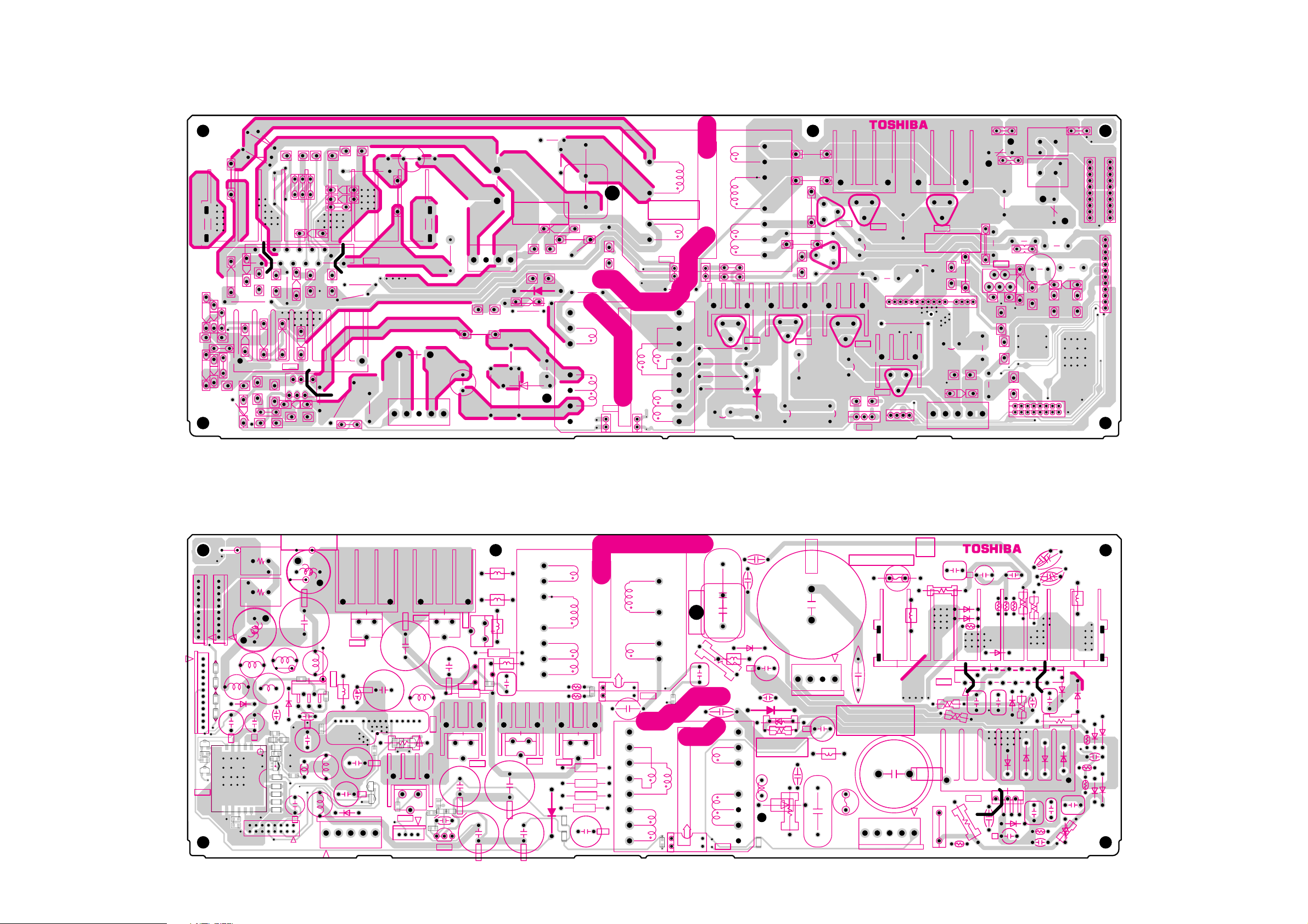
POWER BOARD PD2105A1 (U001)
BOTTOM (FOIL) SIDE
RE14
DE17
DE12
DE08
CE29
DE19
C822
C826
C827
DE13
RE16
C820
CE22
CE23
R812
C819
R814
12
QE01
CE09
R806
D809
DE14
R813
C824
7
DE15
R803
D810
C817
+
D805
R805
Q801A
DE07
+
R807
1
C815
CE17
D806
QE01A
R
RE29
C825
R817
L803
1
Q801
R815
8
0
8
P812B
1
RE18
RE15
C
821
L804
15
14
D811
D812
R809
RE17
DE16
RE13
CE07
CE12
DE09
RE12
CE10
F802
250V F3.15AL
+
5432
FE01
C804
1
+
C810
+
P811B
24
3
RE19
CE16
LE11
CE15
250V F3.15AL
CE18
CAUTION
LIVE AREA
D813
+
C816
CE21
DE06
DE05
RE23
LE12
DE11
RE05
C823
L805
CE11
C803
TE62
R821
C813
QE26
P890
Q826
T862
C899
ZE74
ZE73
ZE75
ZE72
CE82
R873
DE77A
R874
DE77
DE72
+
+
CE85
DE75A
L876
L878
D884A
L875
Z889
L874
C890
DE75
+
CE84
D885
G
C
B
DE73A
+
+
CE86
CE83
Q883
ZE76
D884
QE93
C884
+
LE71
+
QE73
RE74
QE93A
E
C
P813B
4321
+
C889
DE73
CE43
QE83
B
CE74
DE71
DS-7209
23547777
D883A
D883
CE41
CE73
+
CE75
GE50
L884
+
L890
QE40
5
1
CE42
CE40
C883
DE50
R862
R861
L883
L889
L888
LE53
CE50
CE55
+
LE72
LE52
+
+
LE74
CE76
2
115
12345
PJ62A
PJ80A
DE51
LE73
16
CE51
P804
10
10
P805
1
1
1
P803A
++
12
POWER BOARD PD2105A1 (U001)
TOP (COMPONENT) SIDE
GJ99
10
1
12
QE75
QE75
RE82
RE82
RE83
RE83
QE74
QE74
QE71
R862
10
P805
R861
P804
1
1
L888
P803A
DE56
DE56
LE73
DE54
DE54
DE52
+
DE52
DE51
DE55
DE55
CE51
5
QE71
6
PJ80A
RE51
RE52
RE51
16
RE52
GJ84
Q883
D885
C889
P
DE73A
RE46
L876
L878
L875
Z889
P
G
C
B
R890
DE73
+
L874
R890
C890
DE75A
+
DE75
+
CE86
GJ841
C883
L883
L889
GJ889
+
DE50
LE53
CE55
CE50
RE58
RE58
RE56
RE57
RE57
1
CE53
CE53
RE59
RE59
RE60
RE60
QE64
CE52
CE52
CE54
CE54
RE53
RE53
RE55
RE55
RE54
10
RE54
L884
D883A
L890
GJ82
QE40
RE49
RE49
GE50
16
RE73
RE73
CE73
+
+
DE71
2345
D883
CE41
CE75
CE74
QE53
C884
RE78
RE78
RE75
RE75
QE52
QE52
QE53
B
RE92
PJ62A
+
GE51
GE51
1
5
CE42
RE56
CE40
+
LE52
QE64
RE61
LE72
RE61
+
CE76
2
LE74
115
1
RE79
QE93A
RE79
RE92
C
QE93
432
+
P813B
D884A
D884
+
LE71
+
ZE76
1
QE73
QE92
RE74
+
QE92
CE83
RE45
RE45
E
RE46
RE44
RE41
RE41
RE44
CE43
RE43
RE43
1
QE83
CE84
DE72
CE85
R873
R874
DE77
RE42
T862
CE11
C826
C823
D813
L805
C816
TE62
CE24
LE12
CE24
CE21
DE06
DE05
+
RE05
+
P811B
RE19
RE23
CE15
DE11
C803
P890
R821
C813
DE77A
R872
R872
C899
Q826
R816
R816
P
ZE74
P
ZE73
P
ZE75
P
RE40
RE42
ZE72
RE40
+
CE82
RE48
RE48
QE26
LE11
CE18
PD2105
1234
+
CAUTION
LIVE AREA
CE16
FE01
P812B
250V F3.15AL
23590206B
250V F3.15AL
F802
C810
C804
+
L803
-1
C825
C827
R817
D806
D805
R805
1
Q801
C815
R815
R
8
0
8
CE10
QE01
1
RE29
RE15
CE17
RE18
CE09
12534
R807
Q801A
C817
C822
C824
+
R814
C821
CE07
L804
15
D811
D812
C820
CE12
1
E
DE09
DE19
DE16
2
RE13
RE17
RE14
DE12
CE29
DE17
DE08
R809
R
R812
14
C819
R806
DE13
DE14
CE22
+
RE16
CE23
D809
R803
R813
D810
DE07
QE01A
7
DE15
-
26
--
27
-
Page 28

AC-IN BOARD PD2105A2 (U002)
BOTTOM (FOIL) SIDE
31
1
32
4
42
P811A
P813A
D852
SR81
5
LE06
D801A
L806
L807
C806
D801
C805
DE01
5
0
E
C
1
234
P812A
LE07
RE03
DE03
RE04
DE02
CE02
CE13
CE14
C812
C811
CAUTION
+
C8100
LIVE AREA
+
C8110
CE04
L801
DS-7209
R827
R828
23547777
T802
T801
D899
C802
F801
F801B
C801
R801
T6.3A L/250V
F801A
L802
P805B
P800
12
GAP
R899
D899
R801
T801
P800
R899
C801
21
P805B
GAP
T6.3A L/250V
F801B
F801
F801A
C802
GJ88
GJ87
T802
GJ90
GJ89
AC-IN BOARD PD2105A2 (U002)
TOP (COMPONENT) SIDE
RE04
DE03
RE03
P812A
GJ94
LE07
1
DE01
GJ93
LE06
432
5
SR81
CE05
CE04
CAUTION
LIVE AREA
C812
DE02
CE02
CE13
C811
CE14
L802
AC_IN
L801
R853
Q851
D852
Q851
R853
C852
C852
R858
Q852
Q855
R858
R850
R854
Q852
R854
R850
R857
Q855
R857
+-
C805
D801
D801A
C806
+
C8110
PD2105
R828
R827
+
-2
23590206B
P813A
432
R855
R855
Q854
Q854
R859
R859
L807
GJ91
L806
GJ92
1
C851
C851
Q853
R856
R852
R852
R856
Q853
R851
R851
4321
P811A
C8100
-
28
--
29
-
Page 29

SIGNAL BOARD PD2131F (U003)
BOTTOM (FOIL) SIDE
- 30 -
Page 30

SIGNAL BOARD PD2131F (U003)
TOP (COMPONENT) SIDE
- 31 -
Page 31

AV OTHER BOARD PD2119A1 (U004)
BOTTOM (FOIL) SIDE
P819
P818
RE88
DE93
DV01
RV21
RV21 R6635
GR32
RV01
RV53
RV52
RV53
RV51
RV01
RV51
RV52
RV55
QV51
QV51
RV55
GR31
RV54
GR31
RV54
+
CV51
QE91A
1
2
DE91
3
1
2
3
RE88
QE96
DE94
DE95
DE95
R894
R896
R894
R896
D897
D897
D896
R897
D896
R895
R895
R897
RE91
RE84
RE87
RE98
RE91
RE84
RE98
RE87
RE93
QE95
RE93
QE97
RE96
RE96
QE95
DE92
RE95
RE97
5
1
2
PJ87A
PJ63A
RV07
RV07
RV76
RV76
RV77
RV78
RV79
CCC9
RV80
QV54
RV80
RV79
RV77
RV78
QV54
CCC9
R6639
R6639
RC05
RC05
CC10
R6640
R6640
PV23
RC06
RC06
CC10
DS-7209
23547798
RC01
CC01
R6636
RV05
RV02
DV01
RV04
GR32
RV03
RV03
RV30
RV05
RV02
RV04
PH01
RV93
RV30
RV92 RV70
RV93
RE90
RE85
RE85
RE90
CC01 RC01RC03CC05
RV06
RV06
RV92
CC04
R6635
CC04
CV22
CC02
R6636
RC02
CC02
RC02
CC03
LC01
LC02
LC01
LC02
CC03
CV23
+
CV20
CV24
CV20
+
QV52
RV28
RV28
RV59
RV58
RV59
RV58
RV57
RV57
RV56
QV52
RV56
+
+
RV70
CV52
RV31
GR36
GR36
GR33
GR33
RV31
+
CV27
PH02
RV13
B
C
+
CE93
QE98
QE97
1
QE98
E
CE87
QE91
DE90
ZE90
QE94A
RE94
DE99
C684
C684
D670
D670
12
10
GR660
D675
D675
+
C682
D671
D674
D671
D674
R679
C679
R679
+
R678
C681
GR660
GR661
GR661
1
1
4
P602A
CE90
+
C680
CE92
CE91
+
C8001
DE98
DE97
ZE94
12
10
5
QE90A
QE90
B
RE94
C
DE99
QE94
E
P803B
RV13
C678
CV21
CV21
RV38
CV26
C674
R678
RC03 R6638
R6637
RV94
RV94
RV95
CV25
+
Q670
5
+
R6604
R6604
C673
+
R682
C693
R681
C675
D679
D677
C677
R6603
RV38
+
RV95
1
D676
R6603
R6637
Q670A
+
C692
R680
R680
R682
R681
D679
D676
Q662
CC05
R6633
C660
PV17
C6604
+
R6622
C6605
R6622
R6624
R6611
R6623
R6623
Q6604
GR01
R6611
R6629
R6624
R6626
R6626
R6627
R6625
R6628
R6629
R6628
R6620
R6627
R6625
R6702
R6701
R6702
R6701
Q6604
Q6605
Q6605
+
L110
GR01
+
C6603
Q6603
R6633
+
R6610
R6610
+
DE96
1
3
PJ21A
R6620
R6630
C105
R6630
C6602
+
RV120
RV120
C6600
C6601
CV18
+
RV91
RV91
LV16
CV28
+
+
CV13
CV13
CV17
LV16
RV61
RV61
C117
C118
C117
C118
R6634
+
CV19
R661
R6616
R6616
Q655
R6634
Q656
Q656
R661
C668
L101
GR25
GR26
GR25
R663
R663
R660
RV41
R660
GR26
PV22
Q655
R6617
R6617
Q654
R6615
R6615
R662
R662
Q654
D6603
D6603
+
R113
R114
R114
17
R166
R167
RV40
GR27
GR27
P900
1
RV42
RV42
RV41
RV40
9
1
P902
5
GR28
GR28
L191
C116
GR43
C161
GR43
DV43
DV43
GR42
GR42
R165
DV42
DV42
R162
R162
GR41
GR41
DV41
DV45
DV44
R161
DV41
R161
GR44
GR44
DV45
DV44
R4105
R4100
GND
C108
R111
R4105
GR02
C164
Q4102
R4100
C108
R111
R113
C164
Q161
C163
C163
P516A
Q102
Q4102
Q4100
RT10
GR03
GR03
GR02
Q102
RT11
C119
R115
R115
C103
C103
R166
C116
R167
C161
C190
R169
C190
R169
R165
Q162
R163
R163
Q161
C162
R168
R168
C162
R170
R4107
R4106
R4107
R4106
R4101
R4102
R4102
R4101
Q4100
Q4101
GR112
GR112
CC06
R6638
RC04
CC06
R6613
RC04
CC07
LC06
CC08
CC07
LC06
LC05
CC08
LC03
LC04
GR601
GR602
+
LC03
LC04
GR602
C670
+
R677
C671
Q671
Q671
C692
Q672
Q672
+
C693
C685
C691
C685
R684
D677
R686
Q673
C691
R684
Q673
R686
C690
+
R6602
Q663
Q662
Q663
R6602
R6613
Q6601
Q6601
R6632
R6631
Q6602
R6631
LC05
R6612
R6612
GR601
R6614
D6602
R673
C663
R673
C663
C665
R677
C662
C6990
R683
R685
R683
R685
D678
D678
+
+
R6601
R6601
Q6603
R6632
Q6602
R6614
D6602
D6601
D6601
R671
+
C667
R671
R675
R675
C661
R670
C662
R670
R672
R672
R674
R676
R676
C664
R674
C666
C676
CV54
+
RT01
QT06
CT01
GT02
QT06
GT02
QT05
PK05
QT05
RT10
CT09
CT09
RT12
RT12
RT11
QT04
R112
R112
QT04
CT08
CT08
+
C104
+
L102
L102
L191
L103
C114
C115
C113
R108
R107
R108
R107
R103
Q101
R103
Q101
Q162
R104
R104
R105
R164
R105
R170
R164
R4108
Q4103
R4108
Q4103
R4109
R4109
R4103
Q4101
R4103
R4104
R4104
GR612
GR612
RT02
RT01
QT01
RT03
RT02
RT03
QT01
CT01
CT07
RT04
RT04
QT02
QT02
RT07
RT05
GT01
GT01
RT06
RT06
CT06
CT06
CT07
C107
7
+
H001
C114
C115
C112
C112
C113
RT07
RT05
CT02
CT03
CT04
CT02
RT08
CT03
CT04
RT08
RT09
QT03
QT03
RT09
GR05
GR05
GR07
GR07
R101
R101
6
L103
C111
C111
LT01
CT05
CT05
GR06
C102
GR08
+
GR06
GR08
C101
C101
R102
R102
D101
D101
32
C110
C110
GR113
GR113
GR613
GR613
-
32
--
33
-
Page 32

PV23
AV OTHER BOARD PD2119A1 (U004)
TOP (COMPONENT) SIDE
CV54
+
C102
PV22
PK05
LT0 1
+
C107
C104
+
7632
H001
+
PD2119 -1
L105
C119
+
L105
17
1
9
1
5
P516A
GND
+
P900
P902
PJ22A
20
10
PJ22A
23590217B
C668
CV19
CV17
L101
40
30
50
C6602
CV18
PJ60A
C6600
C6601
+
C105
30
40
20
PJ60A
CV28
+
+
QV14
QV14
+
10
PV17
+
C6604
1
8
+
Q6600
9
16
Q6600
+
L110
50
DE96
31
PJ21A
C6605
+
+
C6603
C661
CV25
+
QV15
+
CV26
+
+
+
C671
C6990
1
C673
+
C677
+
P602A
+
+
C660
C667
C666
C665
C664
+
C670
+
C690
+
C676
PH02
5
C675
C678
LV18
LV18
QV15
+
CV27
12
10
Q670
C679
+
+
C674
C681
4
CV52
+
Q670A
C682
+
+
CV24
QV16
CV22
+
QV16
+
CV23
ZE94
5
P803B
CE90
+
CE91
C680
+
CE92
C8001
DE98
P
12
10
DE97
+
QE94
QE90A
QE90
QE94A
DE90
ZE90
PH01
QE91
P
QE91A
+
CE93
CE87
+
RE95
LV17
LV17
PJ63A
CV51
+
DE91
+
DE92
RE97
2
5
PJ87A
P819
1
2
3
1
2
3
P818
QE96
DE94
DE93
-
34
--
35
-
Page 33

LED/RMT BOARD PD2119A2 (U005)
+
23547798
DS-7209
+
19
15
+
+
+
+
C503
L510
C517
C519
C505
L504
L505
P900A
R504
DR05
DR04
CC20
R502
DR03
C501
RR05
R512
R508
R501
GJ16
CC31
RR01
DR01
GJ13
GR34
GJ10
C521
C526
C504
Q504
R514
RR06
GR35
R509
RR04
C516
R506
C514
C524
R505
R511
RR03
DR02
C506
R507
C507
PV90
R516
R515
X501
GC20
C527
P902A
RR02
C502
R504
DR05
DR04
CC20
R502
DR03
C501
RR05
R512
R508
R501
GJ16
CC31
RR01
DR01
GJ13
GR34
GJ10
C521
C526
C504
Q504
R514
RR06
GR35
R509
RR04
C516
R506
C524
R505
R511
RR03
DR02
C506
R507
C507
R516
R515
GC20
RR02
C502
BOTTOM (FOIL) SIDE
PC-IN BOARD PD2119A4 (U007)
BOTTOM (FOIL) SIDE
PC-IN BOARD PD2119A4 (U007)
TOP (COMPONENT) SIDE
P601
P602B
RB22RB24
RB22RB24
11
PJ41A
1
RB10
QB04
RB10
QB04
DB04
CB04
CB04
+
CB01
CB05
+
RB15
RB18
RB18
QB07
QB07
CB38
DB01
CB38
RB09
RB09
RB08
RB08
RB15
DB23
CB02
+
DB23
DB20
CB03
DB22
CB03
DB20
DB22
KB01
23547798
DS-7209
LED/RMT BOARD PD2119A2 (U005)
TOP (COMPONENT) SIDE
4321
P601
14
P602B
R688
P661
PD2119
23590217B
R693
KB01
-2
+
CB02
+
CB01
CB05
++
DB04DB01
+
1234
4
C688 C694
1
C688
C694
R688
P661
R693
111
PJ41A
PD2119 -4
C514
+
38
39
48
L505
Q501
1
+++
L504
P902A
5
Q501
C503
C517
X501
+
+
C527
L510
PV90
25
14
C505
P900A
24
15
1
23590217B
91
C519
KEY BOARD PD2119A3 (U006)
BOTTOM (FOIL) SIDE
DA06
SA06 SA05
RA77
RA77
DA06
RA71 RA72
RA71 SA02RA72SA03
23547798DS-7209
RA73
RA73
RA74
DA01
SA01SA04
RA78
RA74
DA01
RA78
SA07
RA79
DA07
RA79
DA07
PJ42A
1
6
KEY BOARD PD2119A3 (U006)
TOP (COMPONENT) SIDE
SA07 SA01 SA04SA02 SA03 SA06SA05
+
POWER
++++
VOL-DNVOL-UPCH-DNCH-UP
PD2119
-
36
--
-3
23590217B
++
VIDEOMENU
37
-
PJ42A
Page 34

SCHEMATIC DIAGRAM
MODEL : 27WL56P
WARNING : BEFORE SERVICING THIS CHASSIS, READ THE "SERVICE SAFETY PRECAUTIONS" ON PAGE 3 OF THIS MANUAL.
CAUTION : The international hazard symbols " " in the schematic diagram and the parts list designate components which have special characteristics
important for safety and should be replaced only with types identical to those in the original circuit or specified in the parts list. The mounting position of
replacements is to be identical with originals. Before replacing any of these components, read carefully the SERVICE SAFETY PRECAUTIONS on the
MANUAL for this model. Do not degrade the safety of the receiver through improper servicing.
NOTE:
1. RESISTOR Resistance is shown in ohm [K = 1.000, M = 1.000.000]. All resistors are 1/6W and 5%
tolerance carbon resistor, unless otherwise noted as the following marks.
1/2R = Metal or Metal oxide of 1/2 watt 1/2S = Carbon compsistion of 1/2 watt
1RF = Fuse resistor of 1 watt 10W = Cement of 10 watt
K = ±10% G = ±2% F = ± 1%
2. CAPACITOR Unless otherwise noted in schematic, all capacitor values less than 1 are expressed in
?F, and the values more than 1 in pF.
All capacitors are ceramic 50V, unless otherwise noted as the following marks.
Electolytic capacitor Mylar capacitor
3. The parts indicated with " * " have special characteristics, and should be replaced with identical parts only.
4. Voltages read with DIGITAL MULTI-METER from point indicated to chassing ground, using a color bar signal with all
controls at normal, line voltage 220 volts.
5. Waveforms are taken receiving color bar signal with enough sensitivity.
6. Voltage reading shown are nominal values and may vary ±20% except H.V.
-
38
-
Page 35

SCHEMATIC DIAGRAM STRUCTURE:
CONNECTOR ..................................................................................................................................................... 1/48
AV_JACK ............................................................................................................................................................ 2/48
TIF ....................................................................................................................................................................... 3/48
AUDIO_OUT ....................................................................................................................................................... 4/48
REGULATOR ...................................................................................................................................................... 5/48
KEY ..................................................................................................................................................................... 6/48
LED_RMT_HP .................................................................................................................................................... 7/48
PC-IN_BOARD ................................................................................................................................................... 8/48
CONNECTOR(POWER_BOARD) ...................................................................................................................... 9/48
MAIN_POWER(POWER_BOARD) ................................................................................................................... 10/48
SUB_POWER(POWER_BOARD) .................................................................................................................... 11/48
AC-INPUT ......................................................................................................................................................... 12/48
SIGNAL ANALOG IN [SHEET-200]...... 13/48
D IN A [SHEET-300]...... 14/48
D IN B [SHEET-301]...... 15/48
HDMI (Link, I2C) [SHEET-302]...... 16/48
HDMI Rx#2 (Video/Audio) [SHEET-303]...... 17/48
HDMI Rx#3 (PWR,Audio) [SHEET-304]...... 18/48
HDMI AUDIO PLL [SHEET-305]...... 19/48
HDMI AUDIO DAC [SHEET-306]...... 20/48
HDMI AUDIO OUT [SHEET-307]...... 21/48
HDMI CONTROLLER [SHEET-308]...... 22/48
EEPROM1 [SHEET-309]...... 23/48
EEPROM2 [SHEET-310]...... 24/48
MICRO I/O [SHEET-400]...... 25/48
OCM MEMORY I/F [SHEET-401] ...... 26/48
FLASH MEMORY [SHEET-402]...... 27/48
SYNC SEPA [SHEET-403]...... 28/48
E2P OTHER [SHEET-404] ...... 29/48
STD-BY MICOR [SHEET-405]...... 30/48
CORTEZ REG 1 [SHEET-406]...... 31/48
CORTEZ REG 2 [SHEET-407]...... 32/48
CORTEZ REG 3 [SHEET-408]...... 33/48
BOOT CONFIG [SHEET-409]...... 34/48
SERVICE CONNECTOR [SHEET-410]...... 35/48
I2C Switch [SHEET-411]...... 36/48
AUDIO (1/2) [SHEET-600]...... 37/48
(2/2) [SHEET-601]...... 38/48
CORTEZ 1 [SHEET-700]...... 39/48
CORTEZ 2 [SHEET-701]...... 40/48
DDR I/F [SHEET-702]...... 41/48
DDR SDRAM [SHEET-703]...... 42/48
DDR TERMINATION [SHEET-704]...... 43/48
DCDC CONV. [SHEET-802]...... 44/48
LVDS OUT [SHEET-900]...... 45/48
LVDS OUT(SHARP LCD) [SHEET-901] ...... 46/48
Power Connector and Dimming [SHEET-902] ...... 47/48
LVDS Power and Others [SHEET-903]...... 48/48
-
39
-
Page 36

MSP
EXT in
PANEL
CIRCUIT BLOCK DIAGRAM
DDR SDRAM
DDR SDRAM
CORTEZ
OSD
VBI Data
Processor
FLI8532
PANEL I/F
DCDi
MADi
Video
Analog
Scaling
Decoder
End
Front
S
LVD
BEP
(16port)
2nd
Process
Channel
MUX
Digital
656
I2C
Input A
EEPROM
Digital
GPIO
Micro-
Input B
AD
processor
IR I/F
ROM
FLASH
I2C
YCbCr 16bit
MICRO
STAND-BY
UART
IO EXP
POWER BOARD AC INPUT
HDMI
I2C
SIGNAL BOARD
TIF
Non
Audio out
PC IN
HDMI
AV BOARD
-
40
-
Page 37

SPECIFICATIONS
Broadcast systems/channels
PAL-I UHF UK21-UK69
PAL-B/G UHF E21-E69
SECAM-L UHF F21-F69
SECAM-D/K UHF R21-R69
Video Input PAL, SECAM, NTSC 3.58/4.43
External connections
EXT1 Input 21-pin SCART RGB, A/V
EXT2 Input/Output 21-pin SCART A/V, S-video
EXT3 Input (Side)
HDMI Input HDMI connector Digital television and
PC Input Mini D-sub 15-pin Analog RGB signal
VHF E2-E12, S1-S41
VHF F1-F10, B-Q
VHF R1-R12
Selectable output
Phono jack Video
Phono jacks Audio L + R
audio signal
Input Phono jacks Audio L + R
Input Phono jacks Audio L + R
Programme Positions 100
Stereo Nicam
2 carrier system
Visible Screen Size 68cm
(approx.)
Display 16:9
Sound output (at 10% distortion) Main 10W + 10W
Power consumption 130W
as specified in EN60107-1 : 1997
Standby (approx.) <1W
Dimensions 57cm (H) 69cm (W) 10cm (D)
(approx.)
Weight (approx.) 16kg
Headphone socket 3.5mm stereo
Accessories Remote control
2 batteries
(AAA, IEC R03 1.5V)
-
END
-
Page 38

Page 39

SCHEMATIC DIAGRAM
MODEL : 27WL56P
WARNING : BEFORE SERVICING THIS CHASSIS, READ THE "SERVICE SAFETY PRECAUTIONS" ON THE MANUAL FOR THIS MODEL.
CAUTION : The international hazard symbols " " in the schematic diagram and the parts list designate components which have special characteristics
important for safety and should be replaced only with types identical to those in the original circuit or specified in the parts list. The mounting position of
replacements is to be identical with originals. Before replacing any of these components, read carefully the SERVICE SAFETY PRECAUTIONS on the
MANUAL for this model. Do not degrade the safety of the receiver through improper servicing.
NOTE:
1. RESISTOR Resistance is shown in ohm [K = 1.000, M = 1.000.000]. All resistors are 1/6W and 5%
tolerance carbon resistor, unless otherwise noted as the following marks.
1/2R = Metal or Metal oxide of 1/2 watt 1/2S = Carbon compsistion of 1/2 watt
1RF = Fuse resistor of 1 watt 10W = Cement of 10 watt
K = ±10% G = ±2% F = ± 1%
2. CAPACITOR Unless otherwise noted in schematic, all capacitor values less than 1 are expressed in
?F, and the values more than 1 in pF.
All capacitors are ceramic 50V, unless otherwise noted as the following marks.
Electolytic capacitor Mylar capacitor
3. The parts indicated with " * " have special characteristics, and should be replaced with identical parts only.
4. Voltages read with DIGITAL MULTI-METER from point indicated to chassing ground, using a color bar signal with all
controls at normal, line voltage 220 volts.
5. Waveforms are taken receiving color bar signal with enough sensitivity.
6. Voltage reading shown are nominal values and may vary ±20% except H.V.
Page 40

SCHEMATIC DIAGRAM STRUCTURE:
CONNECTOR ..................................................................................................................................................... 1/48
AV_JACK ............................................................................................................................................................ 2/48
TIF ....................................................................................................................................................................... 3/48
AUDIO_OUT ....................................................................................................................................................... 4/48
REGULATOR ...................................................................................................................................................... 5/48
KEY ..................................................................................................................................................................... 6/48
LED_RMT_HP .................................................................................................................................................... 7/48
PC-IN_BOARD ................................................................................................................................................... 8/48
CONNECTOR(POWER_BOARD) ...................................................................................................................... 9/48
MAIN_POWER(POWER_BOARD) ................................................................................................................... 10/48
SUB_POWER(POWER_BOARD) .................................................................................................................... 11/48
AC-INPUT ......................................................................................................................................................... 12/48
SIGNAL ANALOG IN [SHEET-200]...... 13/48
D IN A [SHEET-300]...... 14/48
D IN B [SHEET-301]...... 15/48
HDMI (Link, I2C) [SHEET-302]...... 16/48
HDMI Rx#2 (Video/Audio) [SHEET-303]...... 17/48
HDMI Rx#3 (PWR,Audio) [SHEET-304]...... 18/48
HDMI AUDIO PLL [SHEET-305]...... 19/48
HDMI AUDIO DAC [SHEET-306]...... 20/48
HDMI AUDIO OUT [SHEET-307]...... 21/48
HDMI CONTROLLER [SHEET-308]...... 22/48
EEPROM1 [SHEET-309]...... 23/48
EEPROM2 [SHEET-310]...... 24/48
MICRO I/O [SHEET-400]...... 25/48
OCM MEMORY I/F [SHEET-401] ...... 26/48
FLASH MEMORY [SHEET-402]...... 27/48
SYNC SEPA [SHEET-403]...... 28/48
E2P OTHER [SHEET-404] ...... 29/48
STD-BY MICOR [SHEET-405]...... 30/48
CORTEZ REG 1 [SHEET-406]...... 31/48
CORTEZ REG 2 [SHEET-407]...... 32/48
CORTEZ REG 3 [SHEET-408]...... 33/48
BOOT CONFIG [SHEET-409]...... 34/48
SERVICE CONNECTOR [SHEET-410]...... 35/48
I2C Switch [SHEET-411]...... 36/48
AUDIO (1/2) [SHEET-600]...... 37/48
(2/2) [SHEET-601]...... 38/48
CORTEZ 1 [SHEET-700]...... 39/48
CORTEZ 2 [SHEET-701]...... 40/48
DDR I/F [SHEET-702]...... 41/48
DDR SDRAM [SHEET-703]...... 42/48
DDR TERMINATION [SHEET-704]...... 43/48
DCDC CONV. [SHEET-802]...... 44/48
LVDS OUT [SHEET-900]...... 45/48
LVDS OUT(SHARP LCD) [SHEET-901] ...... 46/48
Power Connector and Dimming [SHEET-902] ...... 47/48
LVDS Power and Others [SHEET-903]...... 48/48
Page 41

MSP
EXT in
PANEL
CIRCUIT BLOCK DIAGRAM
DDR SDRAM
DDR SDRAM
CORTEZ
OSD
VBI Data
Processor
FLI8532
PANEL I/F
DCDi
MADi
Video
Analog
Scaling
Decoder
End
Front
S
LVD
BEP
(16port)
2nd
Process
Channel
MUX
Digital
656
I2C
Input A
EEPROM
Digital
GPIO
Micro-
Input B
AD
processor
IR I/F
ROM
FLASH
I2C
YCbCr 16bit
MICRO
STAND-BY
UART
IO EXP
POWER BOARD AC INPUT
HDMI
I2C
SIGNAL BOARD
TIF
Non
Audio out
PC IN
HDMI
AV BOARD
Page 42

27WL56P
CONNECTOR
(1/48)
Page 43

27WL56P
AV_JACK
(2/48)
Page 44

GR612 GR112
KETSU KETSU
tuner_GND
ENG37A06GF
H001
TIF Type : Horizontal
GR613
KETSU
1.5V (RECEIVING THE SIGNAL)
2.9V (NO SIGTNAL)
GR113
OPEN
tuner_GND
CT01
B6.3V10uF
RT01
100
RT03
68k
RT02
CT05
QT03
B6.3V10uF
B6.3V10uF
CT06
LT01
100u
CT02
OPEN
RT08
150
CT03
OPEN
CT04
150p
RT09
470
2SA1576A
RT07
820
RT04
RT05
1k
100
GT01
CHIP JP
QT01
2SA1576A
27k
QT02
2SC4081-Q
RT06
390
1-B5
1-B5
1-B2,1-D5,2-A7
1-D6,5-A1
SCL1
SDA1
GND
GND
5V2
32V
546
GND
IN1
SW
OUT
123
GT02
CHIP JP
IN2
VCC
RT11
CT08
25V0.1
1k
RT12
QT06
DTC144EUA
RT10
GR05
OPEN
GR07
KETSU
GR08
KETSU
GR06
OPEN
100
470
QT05
2SA1576A
L105
GR02
KETSU
SHORT
GND
SYS_SW2
C117
OPEN
C118
OPEN
SYS_SW1
GND
SYS_SW2
SYS_SW1
GND
SIF
GND
GR03
SHORT
1-B8
1-B8
1-B8
V_TV
1-B3,2-C7
V_TV
GND
GND
TP-12
SCL1
TUNER-GND
P516A
KETSU
C105
10V470
105 C
C101
B25V0.01
L110
KETSU
L101
+
D101
KETSU
220u
CT07
B25V0.01
B6.3V10uF
MM1501XNRE
CT09
TXT_SW
QT04
1-B5
NC(Asia-SW1)
4.86
C114
OPEN
KETSU
C113
KETSU
OPEN
C110
TEM2121M
RM73B1HR00OD
+
C102
10V470
105 C
C111
R101
R102
OPEN
L103
R108
SCL1 SDA1
OPEN
C112
OPEN
C107
OPEN
+
L102
TEM2121M
TEM2121M
R103
R107
RM73B1HR00OD
KETSU
OPEN
C115
C116
R167
L191
C190
0.1uF
Q101
2SC4081-Q
100
R104
10k
R105
27k
171511 131235642 81097 14 16
32.6
C103
B1000p
R114
100
RM73B1HR00OD
KETSU
R111
KETSU
R169
RM73B1HR00OD
(23103272Q)
Q102
OPEN
C108
R165
KETSU
C161
KETSU
KETSU
R166
R113
R112
KETSU
R115
KETSU
R161
KETSU
R163
KETSU
KETSU
Q161
KETSU
C164
+
TP-12
0.01
R168
KETSU
C163
KETSU
R162
KETSU
C119
OPEN
PK05
KETSU
Q162
KETSU
C162
100p
R170
6.8k
R164
KETSU
_SW2
SIF OUT
VIDEO out
(US- NC)
IF out
32V
SIF out
Audio det out
AFT
SDA
SCL
NC(US- IF out)
RF AGC
VT
NC(Asia-SW2)
NCNC5V
GR01
RM73B1HR00OD
SDA1
32V
+
C104
50V4.7
AFT1
AFT1
1-B5
32V
27WL56P
TIF
(3/48)
Page 45

Q670
TA8246AHQ
L/R
1-B6,2-F3
18V
VCC_AUDIO
18V
VCC_AUDIO
MUTE
MUTE
GR660
OPEN
GR661
22k
1-B7
1-B7
R_APRO
R_APRO
GND
L_APRO
L_APRO
GND
D676
MA111
D678
R685 R686
MA111
18k 1k
C676C690
35V100uOPEN
++
C666
R674
OPEN
OPEN
R675
OPEN
R670
4.7k
R671
4.7k
C677
OPEN
C685
B25V0.01
M
OPEN
M
C662
R672
B680p
1.8k
R673
C663
1.8k
B680p
D679
MA111
+
R684
100k
D677
MA111
C660
50V4.7
C661
50V4.7
++
Q673
2SA1162-Y
R683
22k
NC
IN(R)
13587
C670
50V10
R676
OPEN
M
C664
OPEN
R677C667
OPEN
M
C665
OPEN
C693
OPEN
R681
10k
C691
OPEN
R682
100k
A_MUTE
2SC3326-B(TE85,F)
R680
+
C675
50V3.3u
A_MUTE
Q672
10k
GND
C692
OPEN
MUTE
IN (L)
C671
50V10
++
R6604
Q671
2SC3326-B(TE85,F)
MUTE TC
FILTER
642
13.25 26.5 13.2
1k
25V47
C673
+
+
C674
50V1.0
OUT(L)
VCC
9
63V0.10
1/8W 2.2
C678
R678
D670
D671
10
MA111
MA111
OUT(R)
Q670A
35V1000
C680
12
B25V0.01
C684
HEAT SINK
D674
D675
MM
C679
63V0.10
R679
1/8W 2.2
MA111
MA111
35V1000
C8001
11
++
NC
GND
C681
C682
+
+
35V1000
35V1000
GND_AUDIO
L_OUT
R_OUT
GND_AUDIO
GND_AUDIO
L_OUT
R_OUT
GND_AUDIO
26.5V_AUDIO
GND_AUDIO
1-D7,1-D7,1-D8,4-A2,4-B2,5-B1
1-D7
1-D7
1-D7,1-D7,1-D8,4-A2,4-A2,5-B1
26.5V_AUDIO
GND_AUDIO
VCC_GND
1-D8
1-D7,1-D7,1-D8,4-A2,4-B2,5-B1
1-D8
5V1
1-B6
EXT_MUTE
EXT_MUTE
R6601
22k
10k
R6602
Q663
2SC4081-Q
R6603
100k
Q662
RN2404
27WL56P
AUDIO_OUT
(4/48)
Page 46

From SUB_POWER
1-D8
40V
1-D8
18V
VCC_AUDIO
40V
18V
15mA
215mA
ZE94
125V 2A
QE98
2SA1163-GR
RE91
10k
QE97
2SC2713-GR
QE96
2SA1887(FA,F)
RE88
10k
QE95
2SC2412K
QE94A
HEAT SINK
QE94
2SD2396/2SC3852
P
RE98
100k
1R680
RE97
QE94B
RE96
47k
RE93
22k
RE87
47k
RE95
1R1.2k
RE84
1.5k
DE94
MTZJ11B
DE93
MTZJ11B
DE92
MTZJ11B
5mA
+
CE87
50V10
205mA
26.5V_AUDIO
32V
GND
18V1
1-D6,3-B1
32V
GND
1-D4,1-D6,5-A2
18V1
POWER_SW
1-D7
VCC_AUDIO
ZE90
KETSU
P
CE90
63V0.33
RE90RE85
KETSUKETSU
QE90B
QE90A
HEAT SINK
QE90
KIA7809API
QE91A
KETSU
QE91
KETSU
QE91B
DE91
KETSU
DE95
KETSU
CE91
63V0.10
25mA
1-B11-D4,1-D6,5-A1
MM
+
CE92
16V100
180mA
+
CE93
KETSU
DE90
MTZJ12C
9V18V1
12V_FAN
1-D5,1-D6
4-A21-D8
RE94
1/8W270
DE97
MTZJ13C
DE98
MTZJ13C
DE99
1SS355-TE17
GND_AUDIO
27WL56P
REGULATOR
(5/48)
Page 47

KEY_FGND
6
5
GND
ADC_IN2
4
NC
ADC_IN13POWER_KEY
2
1
PJ42A
PLUG_2mm_6P_L\S6B-PH-K-S
HOUSOU
DA06
UDZSTE176.8B
SA06
SA05
VIDEO
PUSH SW 1C1P DC12V 005A
PUSH SW 1C1P DC12V 005A
SA04
VOL-UP
VOL-DOWN
SA03
PUSH SW 1C1P DC12V 005A
RA71
RA72
68k
22k
RA77
10k
SA01
CH-UP
CH-DOWN
SA02
PUSH SW 1C1P DC12V 005A
PUSH SW 1C1P DC12V 005A
RA73
10k
RA78
CHIP JP
DA01
UDZSTE176.8B
SA07
CHIP JP
PUSH SW 1C1P DC12V 005A
PUSH SW 1C1P DC12V 005A
DA07
UDZSTE176.8B
RA74
CHIP JP
RA79
27WL56P
KEY
(6/48)
Page 48

RB18
OPEN
RB15
470
TO SoundAMP Unit
GND
4
3R-OUT
2
L-OUT
1GND
P602B
PLUG_2mm_4P\B4B-PH-K-S
C688
B50V0.01
C694
B50V0.01
R688
1/2R330
R693
1/2R330
P661
EARPHONE J D3.5
GND1
2 SPK-L
3 SPK-R
4 GND
P601
PLUG_2.5mm_4P\B4B-EH-F1A
To SPK CABLE
DB01
SCL-003URC3FXGHJ
POWER
(RED)
DB04
SCL-003MC3FXHJK
QB07
2SC2712Y
RB10
330
2SC2712Y
QB04
25V0.1
NC
1
NC
2
POWER LED
3
4
GND
5
NC
CB04
CB05
7L10V220u
+
ON TIMER
765V1
8
GND
9
RMT_IN
10 3.3V
11
RMT_FGND
B11B-PH-K-S
PJ41A
RB22
KETSU
CB38
25V0.1
000
+
CB01
7L10V220u
RB24
KB01
GPIUE281RK
Vout
Vcc
GND
GP1UE281RK0F
4
5
1
2
3
CB03 CB02
25V0.1 7L10V220u
+
DB20
UDZS TE-17 5.6B
DB23
1SS355-TE17
DB22
1SS355-TE17
RB09
47
RB08
47
27WL56P
LED_RMT_HP
(7/48)
Page 49

L510
OPEN
GJ13
SHORT
GJ16
SHORT
L505
C516
CH11
X501
16.2MHz
TRF4100AT
GC20
CHIP JP
+
C514
16V220u
C524
B0.01
CC31
B1000
38 37 3334 32 3136 35 26 252830 29 27
C517
7L_0.47u
GJ10
OPEN
R515
47k
R516
47k
R509 C519
15k 4.7u
R512
100
R511
OPEN
CC20
OPEN
39
R506
27k
C526
B0.01
C527
R507
2.2u
3.9k
++
C521
B0.022
C501
B0.1
R514
1k
Q504
2SA1576A
40
41
42
43
44
45
46
47
48
X'tal
C3-in
APC-fil
CVBS3/Y3-in
ADDRESS
C2-in
CVBS2/Y2-in
CVBS1/Y_in
C507
OPEN
fil
Comb SYS
Fsc-out
AFC-fil
C1-in
Sync-in
C502
B0.1
R501
6.8k
R2-in
G2-in
B2-in
YS2/YM
CVBS-out
Comb Y-in
VS
Y2-in
Cb2-in
Y/C-VCC
Q501
HS
Digital-GND
Digital-VDD
Comb C-in
/Forced-S
B25V0.01
R502
C503
16V47u
C504
++
A
L504
TRF4100AJ
Cr2-in
SCP
2.7k
R508
Y/C-GND
Cr1-in
Sync-GND
Yvi-out
6.8k
C505
R1-in
121110987654321
16V47u
cr-out
cb-out
G1-in
B1-in
CLP-fil
Cb1-in
Sync-VCC
C506
YS3
13
B0.01
Y-out
Y1-in
24
YS1
23
22
21
+
20
19
18
17
16
15
SDA
SCL
14
R504
R505
100
100
PC-DSUB
R
RR01
1/8W75
RR02 RR05
1/8W75 33
RR03 RR06
1/8W75
GND
PV90
BG
GND
GNDGND
RR04
33
DR02
OPEN
33
KRD-8622
GR34
GR35
SHORT
VH
GND
DR01
OPEN
GND
DR03
OPEN
SHORT
217
DR04
OPEN
DR05
OPEN
P900A
B9B-PH-K-S
BGND
GND3G
GND
4
68H9
GND VGND5R
5
3124
5V2
VOUT
GND
P902A
B5B-PH-K-S
SCL1
SDA1
AV-Y
27WL56P
PC-IN_BOARD
(8/48)
Page 50

BL_VCC
BL_VCC
BL_VCC
BL_VCC
BL_VCC
BL_GND
BL_GND
BL_GND
BL_GND
BL_GND
BL_VCC
BL_VCC
BL_VCC
BL_VCC
BL_VCC
BL_GND
BL_GND
BL_GND
BL_GND
BL_GND
1
2
3
4
5
6
7
8
9
10
P804
B10B-PH-K-S
1
2
3
4
5
6
7
8
9
10
P805
B10B-PH-K-S
BL_Vcc
24
BL_GND
BL_Vcc
BL_GND
2-C8
2-C8
3-D8
3-B8,4-D4
3-D8
5V1
2-D8
1-B2,2-E8
2-D8
2-C8,2-D8,4-E4
POWER_LCD
AC_DETECT
VCC_LCD
POWER_SIG
POWER_LCD
AC_DETECT
GND
5V1
VCC_LCD
GND
5
PJ80A
PLUG_2mm_16P\B16B-PHDSS
NC(PH2S+,STOP_FAN)
2
1
NC(PH2S+,POWER_TV)
4
3
5
6
7
8
9
10
12
11
14
13
16
15
CE76
35V56uF
+
TLN3481GH
POWER_DB
GND
18V
LE74
POWER_DB
18V
3-D8
3-C8
3-A8
2-B1
RECTIFIED(-)_MAIN
2-B1
RECTIFIED(+)_MAIN
2-B1
3-D2
3-D2
3-D2
STARTUP_MAIN
STARTUP_SUB
RECTIFIED(-)_SUB
RECTIFIED(+)_SUB
STARTUP_MAIN
RECTIFIED(-)_MAIN
RECTIFIED(+)_MAIN
STARTUP_SUB
RECTIFIED(-)_SUB
RECTIFIED(+)_SUB
PLUG_3.96mm_4P\B4P-VH
PLUG_3.96mm_5P\B5P-VH
P811B
P812B
4
STARTUP_MAIN
3
RECTIFIED(-)\MAIN
2
NC
1
RECTIFIED(+)\MAIN
1
STARTUP_SUB
2
RECTIFIED(-)\SUB
3
NC
4
RECTIFIED(+)\SUB
5
NC
PJ62A
OPEN
5
F_GND
6.5V3
6.5V3
6.5V
3
F_GND
3.3V
2
3.3V
3.3Vb
5V1
AUDIO_GND
40V
40V
6
40V
9
871112
18V
18V
AUDIO_VCC
AUDIO_VCC
AUDIO_VCC
AUDIO_GND
AUDIO_GND
AUDIO_GND
PROTECT
PROTECT
14
3.3Va
243
1 23154
POWER_SIG
PROTECT
P813B
B4B-PH-K-S
5V1
GND
AUDIO_VCC
29.5
GND
10
GND_HDD
POWER_SW
P803A
PLUG_2mm_12P\B12B-PH-K-S
POWER_SW
AC_DETECT
27WL56P
CONNECTOR(POWER_BOARD)
(9/48)
Page 51

1-A2
1-A2
1-A2
RECTIFIED(+)_MAIN
RECTIFIED(-)_MAIN
STARTUP_MAIN
RECTIFIED(+)_MAIN
RECTIFIED(-)_MAIN
STARTUP_MAIN
35*35mmMAX
F802
250V F3.15AL
F802Z
+
C810
450V220u
LIVE AREA
SHORT
L803
VIN
STR-Z4369
1
10000
C804
2
D805
MTZJ9.1A
CD
CSS
CONT
GND
4
3
MTZJ27C
D806
6
5
R807
1/6P39k
M MM
200V2.2
+
R803
1/6P5.6k
C827
C825
63V1.0
R817
1P220k
D809
7
MTZJ36C
R805
STR-Z4369
DT
63V0.47
C815
1/6P1k
Q801
1/2R10
1312
R809
1/2W 6R8J
C823
2KV470pF
C826
2KV470pF
OUT
14
AG01A
L804
SHORT
C821
C821Z
C822
C822Z
COM
RC
0C
DRIVCC
VCC
8
M
D810
9
MTZJ27C
50V0.22
C817
10
11
R806
1/2R47
50V1000p
100
C819
C824
R815
R808
1/2R100
R812
1/2R680
R814
R813
1/6P27
1/2R39
Q801C
Q801B
Q801A
VB
15
D811
C820
M
50V00.22
D812
MTZJ9.1C
50V100
C816
2kV680PF
2kV820PF
C803
+
630V0.15u
D813
AL01Z
C803Z
L805
TEM2011AA
63V0.33
T862
TPW3572AS
P890
97
10
5
11
L876
TEM2011AA
13
3
2
14
15
16
L878
R873
1/6P1.5k
TEM2011AA
R821
1W6.8
C899
OPEN
Q826
TLP421F(GR)/PS2581L1(D)
41
M
C813
R872
R816
330
23
OPEN
R874
SHORT
C890
63V0.33
R890
L875
TEM2011AA
L874
TEM2011AA
P
Z889
20P5000
D883
RB215T-90
D883C
D883A
D883B
D884
RB215T-90
D884C
D884A
D884B
Q883
SE024N
G
M
1k
D885
FMX-12S(023
+
50V1000
35V2200u
+
+
35V2200u
C883
C884
L890
OPEN
BC
18V
C889
GJ82
620mA
OPEN
LE73
TLN3481AA/GH
35V56uF
OPEN
CE55
RE61
18k_F
L888
TLN3499GH
L889
OPEN
GJ889
SHORT
L883
TLN3551AH
OPEN
COLTLN3639AH
L884
OPEN
COLTLN3639AH
+
L883Z
L884Z
5
4321
RE58
22k_F
1.5k_F
1.5k_F
ON/OFF
GND
GND
Vin
Vin
RE56
RE57
GJ84
GJ841
QE71
CE-1050
SHORT
SHORT
GND
GND
Vset
Vout
Vout
CE53
B25V220n_K
68 7
10 9
RE59
330k
QE64
BD4746G
5
VCCNC
1100mA
6000mA
DE56
MA8300-H
orMA111
DE54
1SS355
5W82 5W82
R862 R861
2500mA
RE55
RE53
39k 1.5k
RE51 RE52
QE75
2SC2412K
CE54
OPEN
4
Vout
B25V220n_K
RE60
SUB
GND
321
47k
CE52
QE74
RE83
RN1403
47k
RE82
47k
RE54
1/8W2.2k
1/8W2.2k
OPEN
GJ99
SHORT
DE55
MA8062-M
SHARP/CMO; MA8062-M
DE52
1SS355
AUDIO_VCC
AUDIO_GND
BL_Vcc
PROTECT
BL_GND
To OBON GND
VCC_LCD
PROTECT
POWER_LCD
AC_DETECT
1-B2
1-B2
1-A1
1-B1,2-D8,4-E4
1-A1
1-A1
orMA111
1-B1,2-C8,4-E4
1-A1
1-A1,1-B2
27WL56P
MAIN_POWER(POWER_BOARD)
(10/48)
Page 52

QE01
STR-W6765
D
LE11
TEM2011AA
CE17
2KV330pF
RE18
RK993DR22J
LIVE AREA
S/GND
DE07
Vcc
MTZJ33B
CE07
RE29
OPEN
63V0.47
SS/OLP
M
M
DE72
FR105-FL
+
CE82
100V47
QE40
LE53
TLN3283D
VIN
4
RE78
OPEN
RE79
OPEN
SI-8050E
Vos
N.C
60mA
DE51
GE51
MTZJ6.8B
16V330
CHIP JP
OPEN
RE49
VAR1
GND
GND
GND
GND
978
RE75
OPEN
VOUT
VAR2
VOUT
VOUT
15 16131110 14
LE72
+
CE73
OPEN
OPEN
OPEN
OPEN
DE71
OPEN
CE75
RE73
OPEN
OPEN
+
CE51
ON/OFF
N.C.
6
5
Vin
GND
SWOut
13542
GE50
TEM2011AA
LE52
33u
20mA
+
CE40
35V220uF
DE75
FMX-12S(023
DE75A
HEAT SINK
DE75B
DE75C
ZE75
P
20P5000
FE01
CE10Z
+
250V F3.15AL
CE10
450V120uF
CE18
1250VH10000p
RE05
2R68k
1-A2
1-A2
1-A2
RECTIFIED(+)_SUB
RECTIFIED(-)_SUB
STARTUP_SUB
RECTIFIED(+)_SUB
RECTIFIED(-)_SUB
STARTUP_SUB
1
DE11
2
RU1P LF-A5
CE15
AL01Z
DE05
1SS244
OPEN
RE19
1/2R8.2
QE01C
QE01B
OCP/BD
FB
QE01A
HEAT SINK
7624531
CE22
OPEN
MTZJ6.8B
M
63V0.10
CE12
+
RE16
MTZJ27B
DE15
CE09
35V3.3
1/6P1k
RE12
1/2R220
470
CE23
MTZJ20B1/6P47k
DE09
DE17
AL01Z
DE08
OPEN
+
CE16
35V56uF
DE14
DE16RE13
AL01Z
RE15
1/6P1k
DE12
AL01Z
RE14
OPEN
DE19
MTZJ10B
DE06
FR105-FL
CE21
OPEN
DE13
RE17
1/6P36k
RE23
1/2R1.5k
CE29
B560p
LE12
50V0.1u
SHORT
CE24
3
4
6
7
8
41
ZE72
20P1000
TE62
TPW3563AS
16
15
14
13
12
11
10
9
QE26
TLP421F(GR)/PS2581L1(D)
23
CE11
OPEN
P
RE48
2.2k
NJM431L
DE73
OPEN
P
ZE73
OPEN
P
ZE74
OPEN
RE40
OPEN
CE43
50V0.1
QE83
DE73C
DE73A
OPEN
DE73B
DE77C
DE77
OPEN
DE77A
OPEN
DE77B
RE45
M
OPEN
RE43
RE44
75k
10k_F
RE46
1.8k_F
+
+
1/8W2.2k
RE42
++
CE86
25V1800u
CE83
OPEN
CE84
OPEN
CE85
25V1800u
LE71
OPEN
ZE76
P
OPEN
RE41
1.5k
M
CE42
DC50VM0.10
CE41
OPEN
DE50
CE50
18V
RE92
OPEN
AK04
OPEN
900mA
QE73
OPEN
VIN
VIN
N.C.
1
3
2
+ +
CE74
OPEN
QE93
QE93A
QE93B
QE93C
RE74
OPEN
QE92
OPEN
QE52
RN2403
QE53
RN1403
15mA
5V1
18V
18V
3.3V
6.5V3
POWER_SW
POWER_DB
40V
1-B2
1-A1,4-D4
1-A2
1-B1
1-B1
1-A2
1-A2
27WL56P
SUB_POWER(POWER_BOARD)
(11/48)
Page 53

L801
TPW2069AS
L806
TLN3481AA/GH
PLUG_3.96mm_5P\B5P-VH
P812A
5
NC
4
RECTIFIED(+)\SUB
3
NC
2
RECTIFIED(-)\SUB
1
STARTUP_SUB
1
RECTIFIED(+)\MAIN
2
NC
3
RECTIFIED(-)\MAIN
4
STARTUP_MAIN
P811A
PLUG_3.96mm_4P\B4P-VH
CE13
AC250V470p
CE14
AC250V470p
SR81
DLS5D1-O(M) 0.15W
Q851
2SC2412K
D852
1SS133
Q852
2SC2412K
R854
1k
R853
10k
GJ93
DE01
D3SB60
DE02
CE02
OPEN
1 5
1
AG01A
DE03
AG01A
RE03
D801
D5SB60, 4001
RE04
1R68k1R68k
C806
250V4700pF
250V4700pF
+-
CE04
250V4700pF
CE05
250V4700pF
C805
D801A
D801B
D801C
++
C8100
C8110
450V220u
KETSU
R827R828
2R10k2R10k
OPEN
GJ94
OPEN
LE07
TLN3481AA/GH
GJ91
OPEN
GJ92
OPEN
L807
TLN3481AA/GH
LE06
TLN3481AA/GH
L802
TPW2070AS
VR37 225J
TNR15G471K
3
C802
AC275V 0.22u
OPEN
OPEN
T802Z
GJ89
GJ90
R801
D899
AC275V0.22u
GJ87
OPEN
GJ88
OPEN
T801Z
C801
F801A
LINENEUTRAL
F801B
F801
T6.3A L/250V
R899
RN14A1A825J
GAP
FUSE HOLDER
FUSE HOLDER
T802
TRF3253AH
T801
TRF3253AH
P805B
1P
C811
AC250V1000p
C812
AC250V1000p
B1000p
5V1
1
GND
2
POWER_SIG
3
PROTECT
4
P813A
B4B-PH-K-S
R856
1k
R850
100
Q855
C852
2SC2412K
R857
470
Q854
2SC2412K
R858
470
R851
1k
R852
470
Q853
2SA1162-Y
R855
470
R859
1k
C851
10V1u
Lock 2P_11.88mm_S
P800
LIVE AREA
27WL56P
AC_INPUT
(12/48)
Page 54

27WL56P
SIGNAL
ANALOG IN
(13/48)
Page 55

27WL56P
SIGNAL
D IN A
(14/48)
Page 56

27WL56P
SIGNAL
D IN B
(15/48)
Page 57

27WL56P
SIGNAL
HDMI (Link,I2C)
(16/48)
Page 58

27WL56P
SIGNAL
HDMI Rx#2 (Video/Audio)
(17/48)
Page 59

27WL56P
SIGNAL
HDMI Rx#3 (PWR,Audio)
(18/48)
Page 60

27WL56P
SIGNAL
HDMI AUDIO PLL
(19/48)
Page 61

27WL56P
SIGNAL
HDMI AUDIO DAC
(20/48)
Page 62

27WL56P
SIGNAL
HDMI AUDIO OUT
(21/48)
Page 63

27WL56P
SIGNAL
HDMI CONTROLLER
(22/48)
Page 64

27WL56P
SIGNAL
EEPROM1
(23/48)
Page 65

27WL56P
SIGNAL
EEPROM2
(24/48)
Page 66

Note: For POWER_DB_O (L: ON) line
When power is ON, GATE is closed until turn ON DB.
During POD STBY mode, it keeping ON, but shut-off circuit includes into DB.
27WL56P
SIGNAL
MICRO I/O
(25/48)
Page 67

402:3A;409:1B
27WL56P
SIGNAL
OCM MEMORY I/F
(26/48)
Page 68

401:1A;409:1B
27WL56P
SIGNAL
FLASH MEMORY
(27/48)
Page 69

27WL56P
SIGNAL
SYNC SEPA
(28/48)
Page 70

27WL56P
SIGNAL
E2P OTHER
(29/48)
Page 71

Note: For I2C Bus lines
(SDA_STBY, SCL_STBY)
: Normally, connecting
to Cortez,
When POD STBY mode,
these are connected
to DB.
27WL56P
SIGNAL STD-BY MICRO
(30/48)
Page 72

27WL56P
SIGNAL
CORTEZ REG 1
(31/48)
Page 73

27WL56P
SIGNAL
CORTEZ REG 2
(32/48)
Page 74

27WL56P
SIGNAL
CORTEZ REG 3
(33/48)
Page 75

27WL56P
SIGNAL
BOOT CONFIG
(34/48)
Page 76

27WL56P
SIGNAL
SERVICE CONNECTOR
(35/48)
Page 77

*I2C Bus Switching of Stand-By Micom
SW1: H at 8V Line (Normally)
; Connect to Cortez
SW2: L at 8V Line (POD STBY state)
; Connect to DB side
27WL56P
SIGNAL
I2C Switch
(36/48)
Page 78

27WL56P
SIGNAL
AUDIO (1/2)
(37/48)
Page 79

8
5
5
27WL56P
SIGNAL
AUDIO (2/2)
(38/48)
Page 80

27WL56P
SIGNAL
CORTEZ 1
(39/48)
Page 81

27WL56P
SIGNAL
CORTEZ 2
(40/48)
Page 82

27WL56P
SIGNAL
DDR I/F
(41/48)
Page 83

27WL56P
SIGNAL
DDR SDRAM
(42/48)
Page 84

27WL56P
SIGNAL
DDR TERMINATION
(43/48)
Page 85

27WL56P
SIGNAL
DCDC CONV.
(44/48)
Page 86

27WL56P
SIGNAL
LVDS OUT
(45/48)
Page 87

R/L U/D
L L Normal Indication
L H Flip Vertical
H L Flip Horizontal
L L Half Turn
27WL56P
SIGNAL LVDS OUT(SHARP LCD)
(46/48)
Page 88

27WL56P
SIGNAL
Power Connector and Dimming
(47/48)
Page 89

27WL56P
SIGNAL
LVDS Power and Others
(48/48)
 Loading...