

Page 1

FILE NO. 020-200515
DOCUMENT CREATED IN JAPAN, July, 2005
SERVICE MANUAL
LCD Color Television
27HLV95
TOSHIBA CORPORATION 2005
-
1
-
Published in Japan, Jul. 2005 (YC)
Page 2

TABLE OF CONTENTS
SERVICE SAFETY PRECAUTIONS .................................................................................................................................... 3
HANDLING THE LCD MODULE .......................................................................................................................................... 5
SERVICE MODE .................................................................................................................................................................. 7
LAYOUT OF MAJOR BOARDS .......................................................................................................................................... 12
MECHANICAL DISASSEMBLY .......................................................................................................................................... 13
EXPLODED VIEW .............................................................................................................................................................. 15
PACKING DISASSEMBLY ................................................................................................................................................. 17
CHASSIS AND CABINET REPLACEMENT PARTS LIST ................................................................................................. 18
PC BOARDS TOP & BOTTOM VIEW ................................................................................................................................ 25
CIRCUIT BLOCK DIAGRAM .............................................................................................................................................. 51
APPENDIX:
SCHEMATIC DIAGRAM
-
2
-
Page 3
GENERAL ADJUSTMENTS
SPECIFIC INFORMATIONS
SERVICE SAFETY PRECAUTIONS
• The caution items shown here describe major safety issues and should always be observed.
• The meanings of the various indications are as follows.
WARNING
CAUTION
* Physical damage means major damage to a home, furnishings and other possessions.
Examples of marks
SHOCK HAZARD
PROHIBIT DISASSEM-
BLING
UNPULUG
Indicates a hypothetical situation in which service personnel and nearby third parties, or even
end users due to a product defect after the service operation is completed, could possibly be in
danger of injury or even death in the event of operational error.
Indicates a hypothetical situation in which service personnel and nearby third parties, or even
end users after the service operation is completed, could possibly be in danger of injury, or
where there could be physical damage in the event of operational error.
The" indicates caution (including danger and warning).
The actual meaning of this caution is indicated inside the
The example shown to the left indicates the danger of "electrical shock".
indicates a forbidden action.
The
The actual meaning of this caution is indicated inside the
The example shown to the left indicates that disassembly is forbidden.
The
-
indicates a forced action (an action that must be performed).
The actual meaning of this forced action is indicated by
The example shown to the left indicates that the power plug must be disconnected.
"
or nearby illustrations or text.
or nearby illustrations or text.
-
or nearby illustrations or text.
-
3
-
Page 4
KEEP CHILDREN
AWAY
UNPULUG
SHOCK HAZARD
USE SPECIFIED
PARTS
CAUTION FOR
WIRING
CAUTION FOR
ASSEMBLING /
WIRING
WARNING
• Always advise users to keep children away.
There is danger of injury to children from tools, disassembled products, etc.
• Always disconnect the power plug before starting work whenever power is not required.
Failure to disconnect the power plug before starting work can result in electrical shock.
• Depending on the model, use an insulation transformer or wear gloves when servicing with the
power on, and disconnect the power plug to avoid electrical shock when replacing parts.
In some cases, alternating current is also impressed in the chassis, so electrical shock is possible if the chassis is contacted with the power on.
• Always use the replacement parts specified for the particular model when making repairs.
The parts used in products have the necessary safety characteristics such as inflammability,
voltage resistance, etc.; therefore, use only replacement parts that have these same characteristics.
Use only the specified parts when the
• Parts mounting and routing of the wiring should be the same as that used originally.
For safety purposes, insulating materials such as tubing or tape is sometimes used and printed
circuit boards are sometimes mounted floating.
Also make sure that wiring is routed and clamped to avoid parts that generate heat and which
use high voltage. Always follow the original scheme.
• After a repair has been completed, reassemble all disassembled parts, and route and reconnect the wiring, in accordance with the original scheme.
Do not allow internal wiring to be pinched by cabinets, panels, etc.
Any error in reassembly or wiring can result in electrical leakage, flame, etc., and may be
hazardous.
mark is included in a circuit diagram or parts list.
CHECK INSULATION
RESISTANCE
PROHIBIT
REMODELING
• After completing the work, disconnect the power plug from the outlet, remove the antenna, turn
on the power switch. Then, use a 500V insulation resistance meter to check the insulation
resistance of the antenna terminal, other metallic parts and between the prongs of the power
plug to make sure that the insulation resistance is 1M 1 or more.
The set will require inspection and repair if the insulation resistance is below this value.
• Never remodel the product in any way.
Remodeling can result in improper operation, malfunction, or electrical leakage and flame,
which may be hazardous
-
4
-
Page 5
GENERAL ADJUSTMENTS
SPECIFIC INFORMATIONS
HANDLING THE LCD MODULE
Safety Precautions
In the event that the screen is damaged or the liquid crystal
(fluid) leaks, do not breathe in or drink this fluid. Also, never
touch this fluid.
Such actions could cause toxicity or skin irritation. If this fluid
should enter the mouth, rinse the mouth thoroughly with water. If the fluid should contact the skin or clothing, wipe off
with alcohol, etc., and rinse thoroughly with water. If the fluid
should enter the eyes, immediately rinse the eyes thoroughly
with running water.
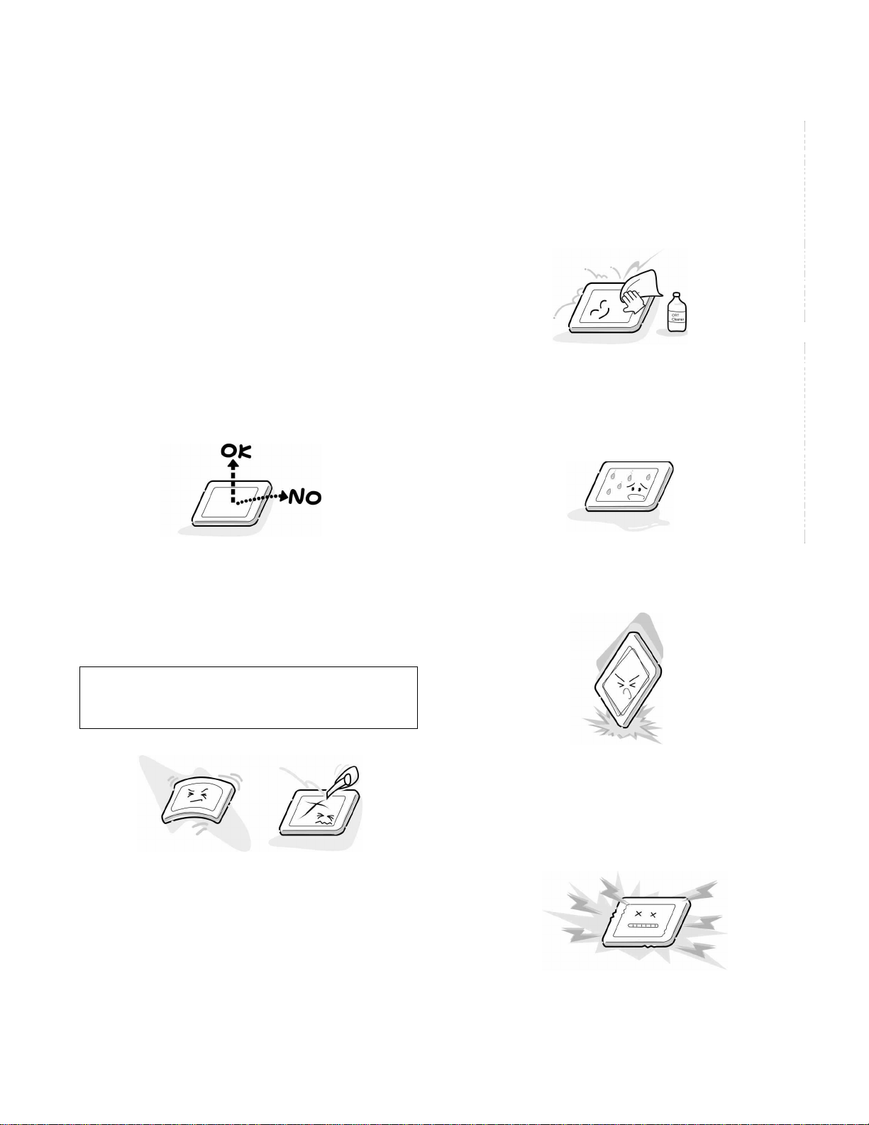
Precautions for Handling the LCD Module
The LCD module can easily be damaged during disassembly
or reassembly; therefore, always observe the following precautions when handling the module.
1. When attaching the LCD module to the LCD cover, position it appropriately and fasten at the position where the
display can be viewed most conveniently.
3. If the panel surface becomes soiled, wipe with cotton or a
soft cloth. If this does not remove the soiling, breathe on
the surface and then wipe again.
If the panel surface is extremely solied, use a CRT cleaner
as a cleaner. Wipe off the panel surface by drop the cleaner
on the cloth. Do not drop the cleaner on the panel. Pay
attention not to scratch the panel surface.
4. Leaving water or other fluids on the panel screen for an
extended period of time can result in discoloration or
stripes. Immediately remove any type of fluid from the
screen.
2. Carefully align the holes at all four corners of the LCD
module with the corresponding holes in the LCD cover
and fasten with screws. Do not strongly push on the module because any impact can adversely affect the performance. Also use caution when handling the polarized screen
because it can easily be damaged.
The metal edges of the LCD module
CAUTION
are sharp, so use caution to avoid injury.
5. Glass is used in the panel, so do not drop or strike with
hard objects. Such actions can damage the panel.
6. CMOS-LSI circuitry is used in the LCD module, so avoid
damage due to static electricity. When handling the module, use a wrist ground or anchor ground.
-
5
-
Page 6
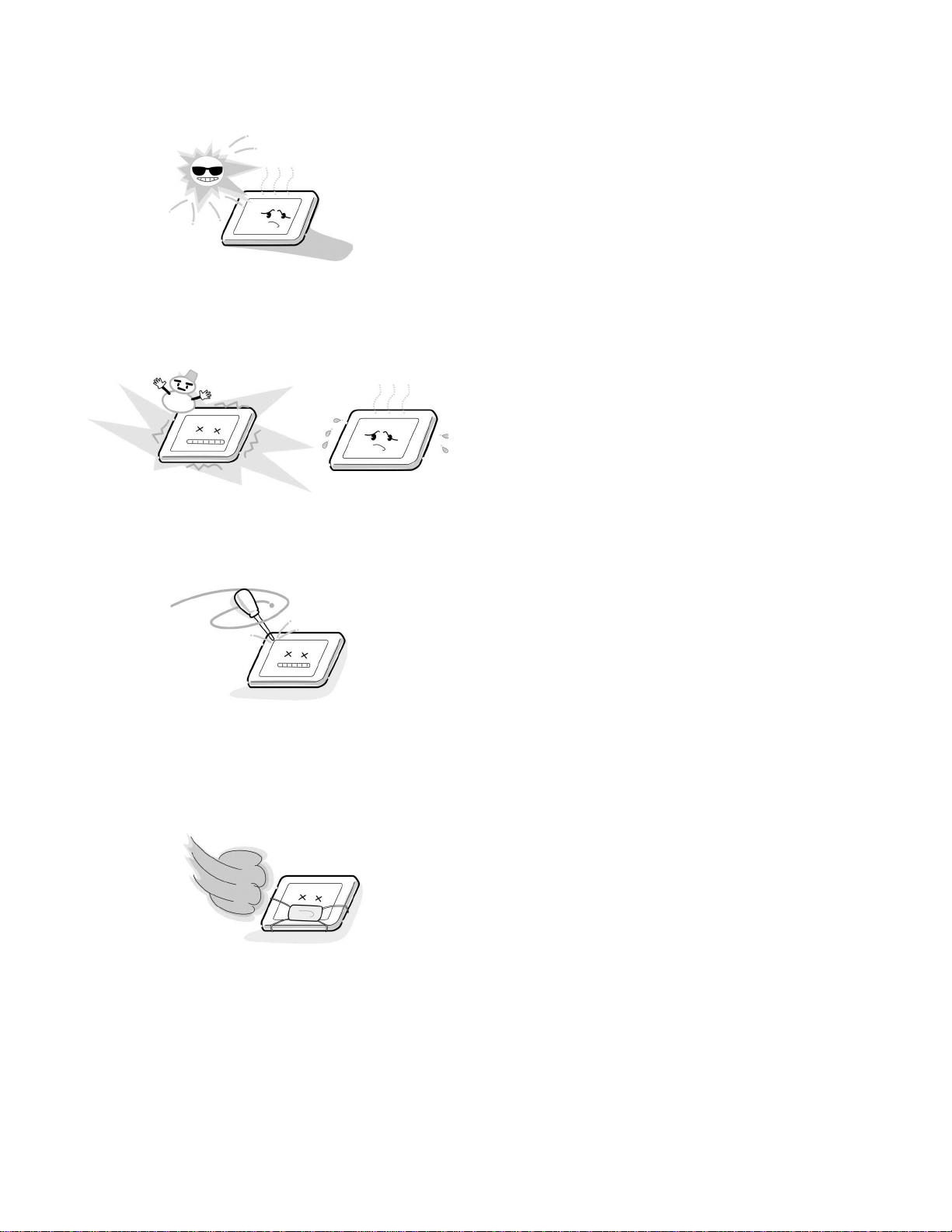
7. Do not expose the LCD module to direct sunlight or strong
ultraviolet rays for an extended period of time.
8. Do not store the LCD module below the temperature conditions described in the specifications. Failure to do so
could result in freezing of the liquid crystal due to cold air
or loss of resilience or other damage.
9. Do not disassemble the LCD module. Such actions could
result in improper operation.
Safety Precautions for Laser Beam (DVD Player)
Do not look into the opening of the disc slot or ventilation
opening of the product to see the source of the laser beam.
It may cause sight damage.
10. When transporting the LCD module, do not use packing
containing epoxy resin (amine) or silicon resin (alcohol or
oxim). The gas generated by these materials can cause
loss of polarity.
-
6
-
Page 7
SERVICE MODE
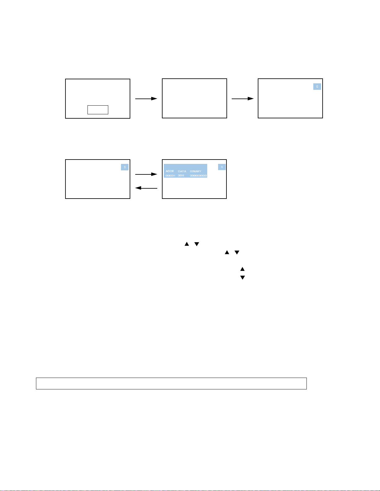
1. ENTERING SERVICE MODE
1) Press MUTE button twice on 2) Press MUTE button again and 3) While pressing the MUTE button,
Remote Control. keep pressing. press MENU button on TV set.
MUTE
2. DISPLAYING THE ADJUSTMENT MENU
1) Press MENU button on Remote Control.
Service mode Adjustment mode
Press
Press
3. KEY FUNCTION IN THE SERVICE MODE
The following key entry during display of adjustment menu provides special functions.
(Service mode display)
Test signal selection : TV/VIDEO button (on Remote)
Selection of the adjustment items : Channel
Change of the data value : Volume W / X (on TV) or
Adjustment menu mode ON/OFF : MENU button (on Remote)
Initialization of the memory : CALL + Channel button on TV ( )
Reset the count of operating protect circuit to “00” :
“RCUT” selection : 1 button
“GCUT” selection : 2 button
“BCUT” selection : 3 button
“CNTX” selection : 4 button
“COLC” selection : 5 button
“UVTT” selection : 6 button
Automatic A/D Adjustment(PC, Component) : 7 button
Self diagnostic display ON/OFF : 9 button
CAUTION : Never try to perform initialization unless you have changed the memory IC.
CALL + Channel button on TV ( )
/ (on TV or Remote)
-----
Color thickness correction
note: Displayed differently as shown below, depending
on the setting of the receiving color system.
COLP (PAL)
COLC (NTSC)
COLS (SECAM)
/ (on Remote)
-
7
-
Page 8
4. SELECTING THE ADJUSTING ITEMS
1) Every pressing of CHANNEL
button for reverse order)
(
5. ADJUSTING THE DATA
1) Pressing of VOLUME W / X , / button will change the value of data in the range from 00H to FFH. The
variable range depends on the adjusting item.
6. EXIT FROM SERVICE MODE
1) Pressing POWER button to turn off the TV once.
INITIALIZATION OF MEMORY DATA
After replacing EEPROM IC, the following initialization is required.
1.Enter the service mode, then select any register item.
2.Press and hold the CALL button on the Remote, then press the CHANNEL
EEPROM IC has been completed.
3. Check the picture carefully. If necessary, adjust any adjustment item above.
Perform “Auto tune” on the owner’s manual.
CAUTION: Never attempt to initialize the data unless EEPROM IC has been replaced.
7. TEST SIGNAL SELECTION
1) Every pressing of TV/VIDEO button on the Remote Control changes the built-in test patterns on screen as described
below in SERVICE MODE.
button in the service mode changes the adjustment items in the order of table-2.
button on the TV. The initialization of
R
All BlackAll White
BSignal off G
Signals Picture
• Red raster
• Green raster
• Blue raster
• All Black
• All White
-
8
-
Page 9
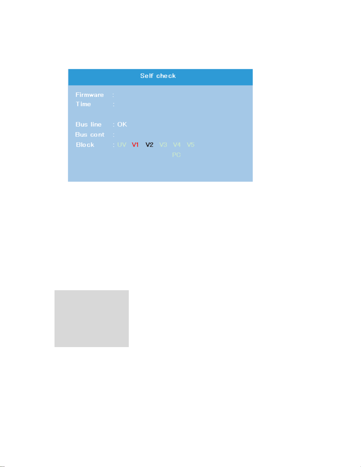
8. SELF DIAGNOSTIC FUNCTION
1) Press “9” button on Remote Control during display of adjustment menu in the service mode.
The diagnosis will begin to check if interface among IC’s is executed properly.
2) During diagnosis, the following displays are shown.
1
2
HLV95_1489
000000
3
4
OK
5
1 Firmware :
Version information of microprocessor
In case of file name : HLV95 and Version : 1489 indicates[HLV95_1489].
2 Time : Total hour of turn the TV on. (Unit : H)
3 Bus line : --"OK" is normal
"SCL-GND"(Red indication) : SCL-GND short circuit
"SDA-GND"(Red indication) : SDA-GND short circuit
"SCL-SDA"(Red indication) : SCL-SDA short circuit
4 Bus cont : --- "OK" is normal.
NG is abnormal(Red indication).
When type name of semiconductor indicates.
5 Block
UV : TV reception mode
V1 : VIDEO 1 input mode
V2 : VIDEO 2 input mode
V3 : ColorStream HD
V4 : HDMI IN
V5 : Buit-in DVD
PC : Personal Computer (PC)
-
9
-
Page 10
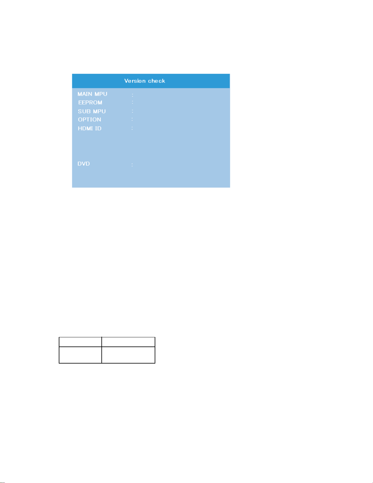
9. VERSION CHECK MODE
1) Press “9” button twice on Remote Control during display of adjustment menu in the service mode. The version of main
MPU will begin to check.
2) During Version Check, the following displays are shown.
1
2
3
4
5
6
HLV95_1489 (U15)
FF
2A
74 00 01 25 00 00
00000155
1A
SHP-27
7
1 MAIN MPU :
Version information of microprocessor
In case of file name : HLV95, Version 1489 for Code Program Version
and (U15) for OSD Version indicates [HLV95_1489(U15)]
2 EEPROM :
Version information of EEPROM : Display 1 byte data.
3 SUB MPU :
Version information of SUB MPU : Display 1 byte data.
4 OPTION :
Option information : Display six numbers of 1 byte data.
5 HDMI ID :
HDMI ID information : Display 4 byte data.
6 DVD :
DVD information : Display 1 byte data.
7 LCD Panel Vender information display
The following Panel Vender and screen size are displayed.
Panel Vender Screen Size(Inch)
CMO -27
SHP -32
Example : SHP-32 indicates that vender is SHP and Screen Size is 32 inch.
-
10
-
Page 11
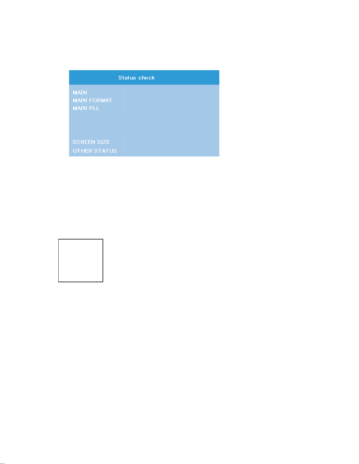
10. STATUS CHECK MODE
1) Press “9” button thrice on Remote Control during display of adjustment menu in the service mode. The status of this
model will begin to check.
2) During Status Check, the following displays are shown.
1
2
3
4
5
ANT1 CABLE 12
480i
06 OF B0 CE 02
NATURAL
0000 0000 0000
1 MAIN :
Main source information :
Display RF position number (0 - 99) on the main screen, or Input Source (ANT1/2/HDMI etc.)
2 MAIN FORMAT :
Display Video and PC format information
3 MAIN PLL :
Main PLL information : Display five numbers of 2 byte data.
4 SCREEN SIZE :
Display the screen size as follows.
Theater Wide 1
Theater Wide 2
Theater Wide 3
FULL
NATURAL
5 OTHER STATUS :
Other status information : Display three numbers of 2 byte data.
-
11
-
Page 12
U104
RF-SW TIF BOARD
U105B
LED-RMT BOARD
LAYOUT OF MAJOR BOARDS
U105A
TN/AV-AOUT BOARD
U101
SIGNAL DVD-LCD BOARD
U105D
PC-IN BOARD
U103
D-TUNER BOARD
U801
POWER BOARD
U105C
KEY-SW BOARD
U802
AC-IN BOARD
U105E
DVD-KEY BOARD
U102
SEINE FOR FPD BOARD
-
12
-
Page 13
P
V15
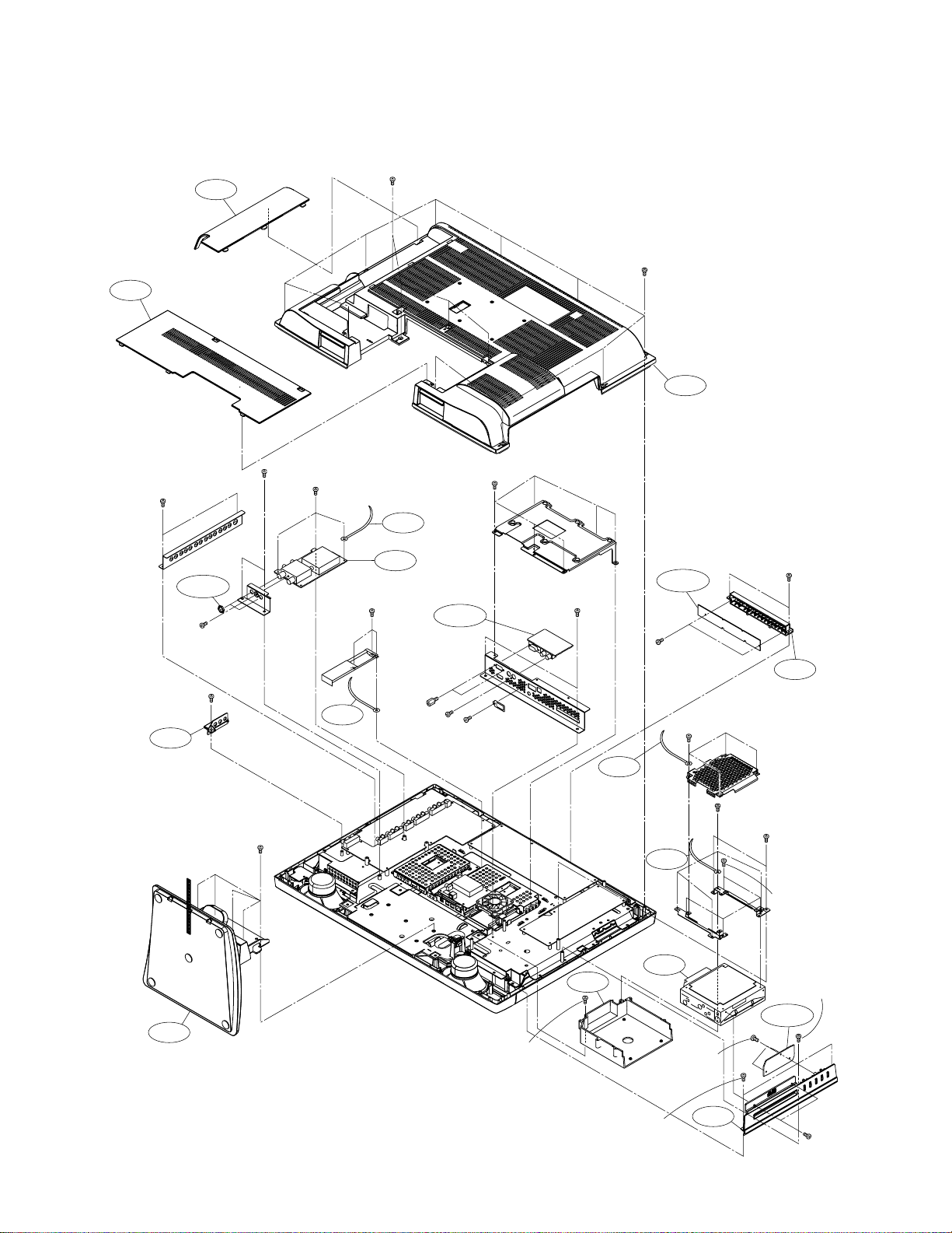
MECHANICAL DISASSEMBLY
P
V15
1. Remove the stand (foot) and back cover.
A450
PP3×8+SW+W SBN ×4
BITTB3×12 SBN ×10
A445
A401
PP5×16 SW+W SBN
×
3
A420
2. Remove the boards (RF-SW TIF, KEY-SW, PC-IN, DVD-KEY) and piece key ass'y.
PP4×12+SW+W SBN ×6
PP4×12+SW+W SBN ×2
PP4×12+SW+W SBN
×
PP4×12+SW+W SBN
PP3×8+SW+W
ECO ×3
PP4×12+SW+W
SBN ×2
H003C
A320
PP08
2
4-40UNC
JFS-4S L=13
×
2
U105D
PP3×8
+SW+
SBN
W
PP3×8
+SW+
SBN
W
U105C
BITTB3×8
ECO ×2
PP08
PP3×8+SW+W SBN
×
U104
PP3×8
+SW+
W SBN
PP3×8
+SW+
×
3
W ECO
PP08
BD01
PP08
PP3×8
+SW+
W SBN
A525
BITTB3×12 SBN
BITTB3×8
×
ECO
×
2
3
BITTB3×12 SBN
×
2
A340
4
BITTB3×8 ECO
×
4
PP3×8
+SW+
W SBN
×
2
PP3×8
+SW+
W SBN
×
4
PP3×8
+SW+
W SBN
U105E
A507
PP3×8+SW+W
×
SBN
2
-
13
-
Page 14
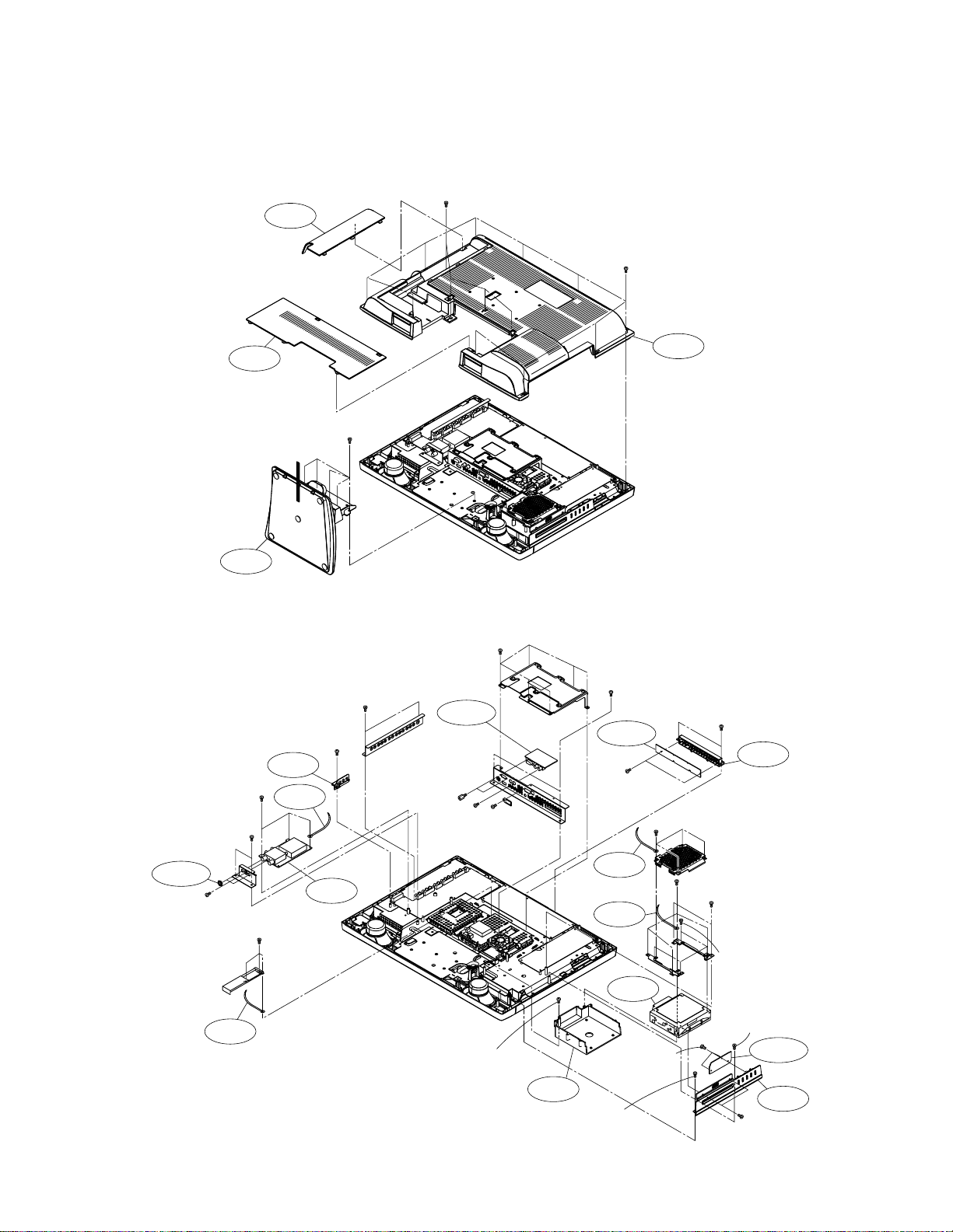
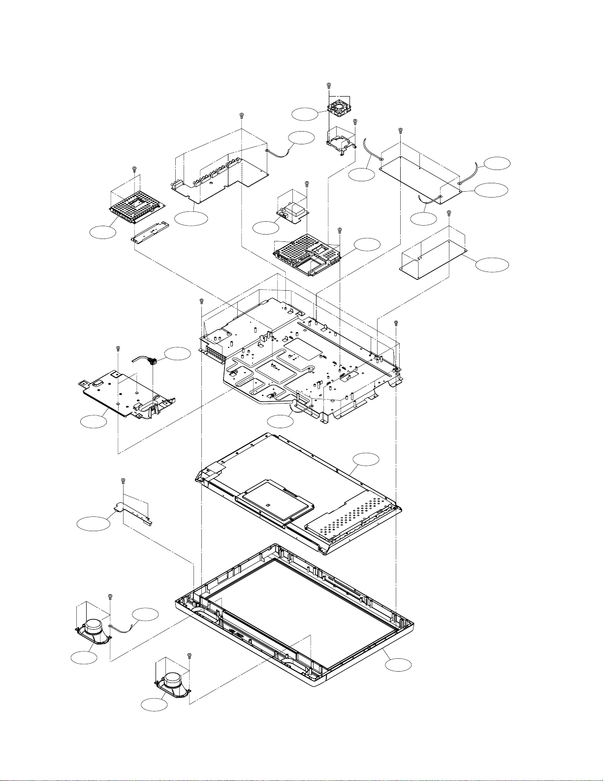
PV1
5
3. Remove the boards (SIGNAL DVD-LCD, SEINE FOR FPD, D-TUNER, TN/AV-AOUT, LED-RMT,
POWER, AC-IN) and speaker.
PP3×8+SW+W ECO ×3
BITTB3×8 ECO
×
2
U105B
PP3×8+SW+W SBN
×
2
A315
4. Remove the display.
PP3×8+SW+W ECO
×
6
U105A
U101
P801
PP08
U103
UF03
PP3×8
SW+W
ECO ×4
PP4×20+SW+W SBN ×2
PP3×8+SW+W ECO ×4
+
PP08
PP3×8+SW+W ECO
×
PP3×8
+
SW+W
ECO ×3
U102
PP08
PP3×8+SW+W ECO
×
U802
5
PP08
U801
5
PP4×12+SW+W SBN
×4
BITTB4×16 SBN ×4
PP08
W661
BITTB4×16 SBN
×
4
W661
PP08
BITTB4×16 SBN
×
14
B001
A201
-
14
-
Page 15
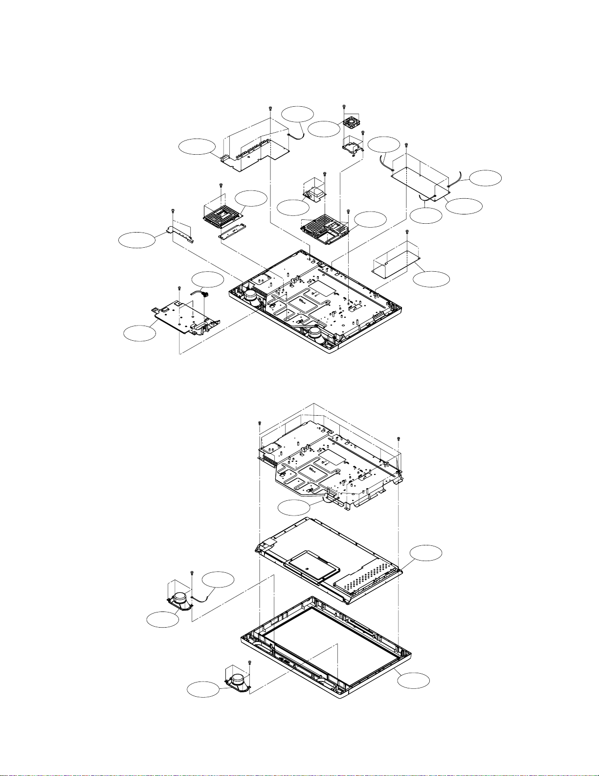
1. Chassis Block
PV15
A450
A445
EXPLODED VIEWS
PP3×8+SW+W SBN
×
4
BITTB3×12 SBN
×
10
A401
PP4×12+SW+W SBN
×
2
H003C
PP3×8+SW+W
SBN
PP4×12+SW+W
A320
SBN
PP5×16 SW+W SBN
×
5
PP4×12+SW+W SBN
×
2
PP3×8+SW+W ECO
×
3
U104
PP3×8+SW+W
ECO
×
PP08
PP08
3
4-40UNC
JFS-4S L=13
×
2
PP3×8
+SW+
SBN
U105D
PP3×8+SW+W
W
SBN
PP4×12+SW+W SBN ×6
PP4×12+SW+W
×
SBN
2
PP08
U105C
BITTB3×12
SBN ×2
PP3×8+SW+W SBN
×
4
PP08
BITTB3×12 SBN
×
2
A340
BITTB3×8 ECO
×
4
PP3×8
+SW+
×
2
PP3×8
+SW+
×
4
W SBN
W SBN
A420
-
15
PP3×8
+SW+
-
W SBN
A525
BITTB3×12 SBN
×
BD01
BITTB3×8
×
ECO
2
3
A501
PP3×8
+SW+
W SBN
U105E
PP3×8+SW+W
×
SBN
2
Page 16
P
V
15
2. Main Block
PP3×8+SW+W ECO
×
6
PP4×20+SW+W
×
SBN
2
UF03
PP08
PP3×8+SW+W ECO ×4
PP3×8+SW+W ECO
×
5
PP3×8+SW+W ECO
×
3
U101
PP4×12+SW+W SBN
×
4
PP3×8+SW+W SBN
×
2
A315
U105A
P801
PP3×8+SW+W
ECO
U103
PP08
×
PP08
4
PP08
U801
PP3×8+SW+W ECO
PP3×8+SW+W
ECO
×
3
PP08
×
5
U102
U802
BITTB4×16 SBN
×
14
BITTB3×8 ECO
×
2
U105B
BITTB4×16 SBN
×
4
W661
PP08
BITTB4×16 SBN
×
W661
B001
4
A201
-
16
-
Page 17
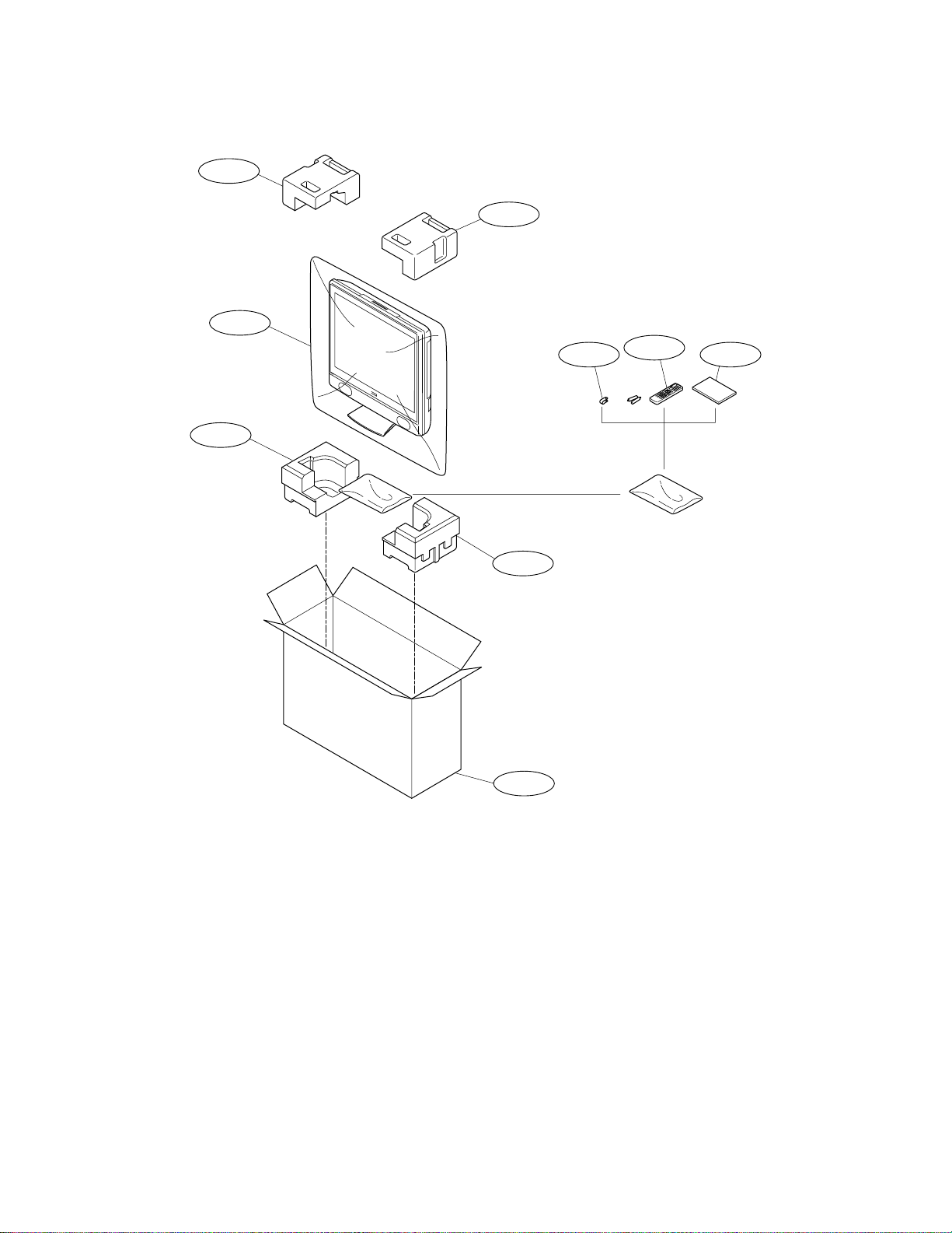
A702A
A703
A702B
PACKING DISASSEMBLY
A702A
Y170 Y101
K902
A702B
A701A
-
17
-
Page 18
CHASSIS AND CABINET REPLACEMENT PARTS LIST
WARNING: BEFORE SERVICING THIS CHASSIS, READ THE “SERVICE SAFETY PRECAUTIONS” ON PAGE 3 OF THIS
MANUAL.
CAUTION: The international hazard symbols " " in the schematic diagram and the parts list designate components which
have special characteristics important for safety and should be replaced only with types identical to those in the original
circuit or specified in the parts list. The mounting position of replacements is to be identical with originals. Before replacing
any of these components, read carefully the SERVICE SAFETY PRECAUTIONS. Do not degrade the safety of the receiver
through improper servicing.
NOTICE:
•
The part number must be used when ordering parts, in order to assist in processing, be sure to include the Model
number and Description.
•
The PC board assembly with ∗ mark is no longer available after the end of the production.
Model : 27HLV95
Capacitors ............. CD : Ceramic Disk PF : Plastic Film EL : Electrolytic
Resistors ............... CF : Carbon Film CC : Carbon Composition MF : Metal Film
OMF : Oxide Metal Film VR : Variable Resistor FR : Fusible Resistor
(All CD and PF capacitors are ±5%, 50V and all resistors, ±5%, 1/6W unless otherwise noted.)
Location
Parts No. Description
No.
CAPACITORS
C102 76073019 ELECTROLYTIC, 10V 470UF M 3A
C103 76109102 CERAMIC CHIP, 50V B 1000PF K
C104 76073084 ELECTROLYTIC, 50V 4.7UF M 3A
C105 76073019 ELECTROLYTIC, 10V 470UF M 3A
C150 76073041 ELECTROLYTIC, 16V 470UF M 3A
C151 76109103 CERAMIC CHIP, 50V B 0.01UF K
C152 76109103 CERAMIC CHIP, 50V B 0.01UF K
C153 76109103 CERAMIC CHIP, 50V B 0.01UF K
C161 76109102 CERAMIC CHIP, 50V B 1000PF K
C162 76105101 CERAMIC CHIP, 50V CH 100PF J
C164 76092730 CERAMIC CHIP, 16V B 0.1UF K
C168 76109103 CERAMIC CHIP, 50V B 0.01UF K
C169 76109103 CERAMIC CHIP, 50V B 0.01UF K
C660 76669479 ELECTROLYTIC, 50V 4.7UF M
C661 76669479 ELECTROLYTIC, 50V 4.7UF M
C662 76109681 CERAMIC CHIP, 50V B 680PF K
C663 76109681 CERAMIC CHIP, 50V B 680PF K
C668 76109102 CERAMIC CHIP, 50V B 1000PF K
C669 76109102 CERAMIC CHIP, 50V B 1000PF K
C670 76669100 ELECTROLYTIC, 50V 10UF M
C671 76669100 ELECTROLYTIC, 50V 10UF M
C673 76619102 ELECTROLYTIC CHIP, 16V 47UF M
C674 76092731 CERAMIC CHIP, 16V B 1UF K
C677 76092731 CERAMIC CHIP, 16V B 1UF K
C678 76285104 CERAMIC CHIP, 50V B 0.1UF K
C679 76285104 CERAMIC CHIP, 50V B 0.1UF K
C680 76073073 ELECTROLYTIC, 35V 2200UF M 3A
C681 76073073 ELECTROLYTIC, 35V 2200UF M 3A
C682 76073073 ELECTROLYTIC, 35V 2200UF M 3A
C684 76109103 CERAMIC CHIP, 50V B 0.01UF K
C685 76619113 ELECTROLYTIC CHIP, 50V 1UF M
C690 76669101 ELECTROLYTIC, 50V 100UF M
C691 76092463 CERAMIC CHIP, 16V B 0.22UF K
C692 76092463 CERAMIC CHIP, 16V B 0.22UF K
C801 76503507 PLASTIC FILM, AC275V 0.22UF K
C802 76503507 PLASTIC FILM, AC275V 0.22UF K
C803 76503250 PLASTIC FILM, 400V 0.22UF M, 7E2G224J-SC
C804 76214103 CERAMIC DISC, 500V B 0.01UF K
C805 76092281 CERAMIC DISC, AC250V E 4700PF
C806 76092281 CERAMIC DISC, AC250V E 4700PF
Location
Parts No. Description
No.
C810 76073233 ELECTROLYTIC, 200V 560UF M
C811 76092569 CERAMIC DISC, AC250V E 2200PF M
C812 76092569 CERAMIC DISC, AC250V E 2200PF M
C813 76503047 PLASTIC FILM, 63V 0.33UF J
C815 76503049 PLASTIC FILM, 63V 0.47UF J
C816 76073183 ELECTROLYTIC, 35V 220UF M
C817 76567224 PLASTIC FILM, 50V 0.22UF J
C819 76214101 CERAMIC DISC, 500V B 100PF K
C820 76567224 PLASTIC FILM, 50V 0.22UF J
C821 76092343 CERAMIC DISC, 2KV 680PF K
C822 76092344 CERAMIC DISC, 2KV 820PF K
C823 76092341 CERAMIC DISC, 2KV R 470PF K
C824 76591102 PLASTIC FILM, 50V 1000PF J
C825 76503053 PLASTIC FILM, 63V 1UF J
C826 76092341 CERAMIC DISC, 2KV R 470PF K
C827 76678229 ELECTROLYTIC, 200V 2.2UF M
C851 76092538 CERAMIC CHIP, 10V F 1UF Z
C852 76109102 CERAMIC CHIP, 50V B 1000PF K
C883 76073193 ELECTROLYTIC, 35V 2200UF M
C884 76073193 ELECTROLYTIC, 35V 2200UF M
C888 76105101 CERAMIC CHIP, 50V CH 100PF J
C889 76073094 ELECTROLYTIC, 50V 1000UF M 3A
C890 76503047 PLASTIC FILM, 63V 0.33UF J
C8110 76073233 ELECTROLYTIC, 200V 560UF M
CB01 76202221 ELECTROLYTIC, 10V 220UF M 7L 3A
CB02 76202221 ELECTROLYTIC, 10V 220UF M 7L 3A
CB03 76100104 CERAMIC CHIP, 25V F 0.1UF Z
CB04 76100104 CERAMIC CHIP, 25V F 0.1UF Z
CB05 76202221 ELECTROLYTIC, 10V 220UF M 7L 3A
CB38 76100104 CERAMIC CHIP, 25V F 0.1UF Z
CC16 76109102 CERAMIC CHIP, 50V B 1000PF K
CC17 76109102 CERAMIC CHIP, 50V B 1000PF K
CD11 76073181 ELECTROLYTIC CE04P 35V 56UF M 3A
CD21 76666470 ELECTORLYTIC, 16V 47UF M 3A
CD22 76539474 PLASTIC FILM, 50V 0.47UF J
CD23 76666470 ELECTORLYTIC, 16V 47UF M 3A
CD41 76105330 CERAMIC CHIP, 50V CH 33PF J
CD42 76105330 CERAMIC CHIP, 50V CH 33PF J
CD43 76105330 CERAMIC CHIP, 50V CH 33PF J
CD45 76105330 CERAMIC CHIP, 50V CH 33PF J
CD46 76105330 CERAMIC CHIP, 50V CH 33PF J
-
18
-
Page 19
Location
Parts No. Description
No.
CD47 76105330 CERAMIC CHIP, 50V CH 33PF J
CD48 76105330 CERAMIC CHIP, 50V CH 33PF J
CD61 76105330 CERAMIC CHIP, 50V CH 33PF J
CD62 76105330 CERAMIC CHIP, 50V CH 33PF J
CD63 76105330 CERAMIC CHIP, 50V CH 33PF J
CD64 76105330 CERAMIC CHIP, 50V CH 33PF J
CD65 76105330 CERAMIC CHIP, 50V CH 33PF J
CD66 76105330 CERAMIC CHIP, 50V CH 33PF J
CD67 76105330 CERAMIC CHIP, 50V CH 33PF J
CD81 76619040 ELECTROLYTIC CHIP, 16V 10UF M 3A
CD82 76619040 ELECTROLYTIC CHIP, 16V 10UF M 3A
CD83 76109102 CERAMIC CHIP, 50V B 1000PF K
CD84 76109102 CERAMIC CHIP, 50V B 1000PF K
CD85 76105221 CERAMIC CHIP, 50V CH 220PF J
CD87 76092731 CERAMIC CHIP, 16V B 1UF K
CD88 76105221 CERAMIC CHIP, 50V CH 220PF J
CD89 76105221 CERAMIC CHIP, 50V CH 220PF J
CD90 76105221 CERAMIC CHIP, 50V CH 220PF J
CD91 76619040 ELECTROLYTIC CHIP, 16V 10UF M 3A
CD92 76109102 CERAMIC CHIP, 50V B 1000PF K
CD93 76105101 CERAMIC CHIP, 50V CH 100PF J
CD94 76109102 CERAMIC CHIP, 50V B 1000PF K
CD95 76619040 ELECTROLYTIC CHIP, 16V 10UF M 3A
CD96 76619040 ELECTROLYTIC CHIP, 16V 10UF M 3A
CE04 76092281 CERAMIC DISC, AC250V E 4700PF
CE05 76092281 CERAMIC DISC, AC250V E 4700PF
CE07 76503049 PLASTIC FILM, 63V 0.47UF J
CE09 76668339 ELECTROLYTIC, 35V 3.3UF M 3A
CE10 76073217 ELECTROLYTIC, 200V 560UF M
CE12 76503041 PLASTIC FILM , 63V 0.1UF J
CE13 76092561 CERA CAP B 250V 101 CD70-B2GA101KYNS
CE14 76092561 CERA CAP B 250V 101 CD70-B2GA101KYNS
CE15 76092337 CERAMIC DISC, 2KV 220PF K
CE16 76073181 ELECTROLYTIC CE04P 35V 56UF M 3A
CE17 76092339 CERAMIC DISC, 2KV 330PF K
CE18 76503253 PLASTIC FILM, 1250VH 0.01UF H
CE23 76214471 CERAMIC DISC, 500V B 470PF K
CE24 76285104 CERAMIC CHIP, 50V B 0.1UF K
CE26 76795101 ELECTROLYTIC, 25V 100UF M
CE29 76436331 CERAMIC DISC, 50V SL 330PF J
CE40 76073183 ELECTROLYTIC, 35V 220UF M
CE42 76539104 PLASTIC FILM, 50V 0.1UF J
CE43 76503041 PLASTIC FILM , 63V 0.1UF J
CE51 76617023 ELECTROLYTIC, 16V 330UF M
CE52 76092179 CERAMIC CHIP, 25V B 0.22UF K
CE53 76092179 CERAMIC CHIP, 25V B 0.22UF K
CE55 76073181 ELECTROLYTIC CE04P 35V 56UF M 3A
CE73 76073186 ELECTROLYTIC, 35V 470UF M
CE74 76073189 ELECTROLYTIC, 35V 1000UF M
CE75 76073128 ELECTROLYTIC, 6.3V 1000UF M
CE76 76073181 ELECTROLYTIC CE04P 35V 56UF M 3A
CE82 76676470 ELECTROLYTIC, 100V 47UF M 3A
CE83 76073175 ELECTROLYTIC, 25V 1800UF M
CE84 76073178 ELECTROLYTIC, 25V 3300UF M
CE85 76073190 ELECTROLYTIC CE04P 35V 1200UF M 3A
CE86 76073190 ELECTROLYTIC CE04P 35V 1200UF M 3A
CE87 76669100 ELECTROLYTIC, 50V 10UF M
CE90 76503047 PLASTIC FILM, 63V 0.33UF J
CE91 76503041 PLASTIC FILM , 63V 0.1UF J
CE92 76794101 ELECTROLYTIC, 16V 100UF M
CE94 76503047 PLASTIC FILM, 63V 0.33UF J
CE95 76503041 PLASTIC FILM , 63V 0.1UF J
CE96 76794101 ELECTROLYTIC, 16V 100UF M
CS10 76092628 CERAMIC CHIP, 6.3V B 10UF K
CS11 76092628 CERAMIC CHIP, 6.3V B 10UF K
CS12 76109473 CERAMIC CHIP, 25V B 0.047UF K
Location
Parts No. Description
No.
CS15 76092628 CERAMIC CHIP, 6.3V B 10UF K
CS16 76092628 CERAMIC CHIP, 6.3V B 10UF K
CS40 76092611 CERAMIC CHIP, 6.3V B 2.2UF K
CS41 76092611 CERAMIC CHIP, 6.3V B 2.2UF K
CS42 76092611 CERAMIC CHIP, 6.3V B 2.2UF K
CS43 76092611 CERAMIC CHIP, 6.3V B 2.2UF K
CS44 76092611 CERAMIC CHIP, 6.3V B 2.2UF K
CS45 76092611 CERAMIC CHIP, 6.3V B 2.2UF K
CS46 76092611 CERAMIC CHIP, 6.3V B 2.2UF K
CS47 76092611 CERAMIC CHIP, 6.3V B 2.2UF K
CS50 76092611 CERAMIC CHIP, 6.3V B 2.2UF K
CS51 76092611 CERAMIC CHIP, 6.3V B 2.2UF K
CS52 76092611 CERAMIC CHIP, 6.3V B 2.2UF K
CS53 76092611 CERAMIC CHIP, 6.3V B 2.2UF K
CS54 76092611 CERAMIC CHIP, 6.3V B 2.2UF K
CS55 76092611 CERAMIC CHIP, 6.3V B 2.2UF K
CS56 76092611 CERAMIC CHIP, 6.3V B 2.2UF K
CS57 76619102 ELECTROLYTIC CHIP, 16V 47UF M
CS64 76619101 ELECTROLYTIC CHIP, 16V 22UF M
CS82 76092611 CERAMIC CHIP, 6.3V B 2.2UF K
CS501 76619100 ELECTROLYTIC CHIP, 16V 10UF M
CS502 76092726 CERAMIC CHIP, 10V B 2.2UF K
CS503 76619100 ELECTROLYTIC CHIP, 16V 10UF M
CS504 76105470 CERAMIC CHIP, 50V CH 47PF J
CS505 76105470 CERAMIC CHIP, 50V CH 47PF J
CV10 76109102 CERAMIC CHIP, 50V B 1000PF K
CV59 76105220 CERAMIC CHIP, 50V CH 22PF J
CV61 76105270 CERAMIC CHIP, 50V CH 27PF J
CV62 76105330 CERAMIC CHIP, 50V CH 33PF J
CV63 76092730 CERAMIC CHIP, 16V B 0.1UF K
CV68 76092621 CERAMIC CHIP, 10V B 1UF K
CV69 76092621 CERAMIC CHIP, 10V B 1UF K
CV72 76794471 ELECTROLYTIC, 16V 470UF M
CV74 76666101 ELECTROLYTIC, 16V 100UF M 3A
CV76 76100104 CERAMIC CHIP, 25V F 0.1UF Z
RESISTORS
R103 76011101 CHIP, 1/20W 100 OHM J
R104 76011103 CHIP, 1/20W 10K OHM J
R105 76011273 CHIP, 1/20W 27K OHM J
R107 76000445 CHIP JUMPER, 1608TYPE
R108 76000445 CHIP JUMPER, 1608TYPE
R110 76011682 CHIP, 1/20W 6.8K OHM J
R114 76000445 CHIP JUMPER, 1608TYPE
R161 76011102 CHIP, 1/20W 1K OHM J
R165 76011392 CHIP, 1/20W 3.9K OHM J
R166 76011472 CHIP, 1/20W 4.7K OHM J
R167 76011101 CHIP, 1/20W 100 OHM J
R168 76011101 CHIP, 1/20W 100 OHM J
R664 76011104 CHIP, 1/20W 100K OHM J
R665 76011104 CHIP, 1/20W 100K OHM J
R670 76011472 CHIP, 1/20W 4.7K OHM J
R671 76011472 CHIP, 1/20W 4.7K OHM J
R672 76011182 CHIP, 1/20W 1.8K OHM J
R673 76011182 CHIP, 1/20W 1.8K OHM J
R678 76871229 CHIP, 1/8W 2.2 OHM J
R679 76871229 CHIP, 1/8W 2.2 OHM J
R680 76011473 CHIP, 1/20W 47K OHM J
R681 76011473 CHIP, 1/20W 47K OHM J
R683 76011223 CHIP, 1/20W 22K OHM J
R684 76011104 CHIP, 1/20W 100K OHM J
R685 76011183 CHIP, 1/20W 18K OHM J
R686 76011102 CHIP, 1/20W 1K OHM J
R688 76552331 OXIDE METAL FILM, 1/2W 330 OHM J
R691 76000445 CHIP JUMPER, 1608TYPE
R693 76552331 OXIDE METAL FILM, 1/2W 330 OHM J
-
19
-
Page 20
Location
Parts No. Description
No.
R801 76004716 METAL GLAZE, 1/2W 2.2M OHM J
R803 76366182 CARBON FILM, 1/6W 1.8K OHM J
R805 76366102 CARBON FILM, 1/6W 1K OHM J
R806 76552470 OXIDE METAL FILM, 1/2W 47 OHM J
R807 76366153 CARBON FILM, 1/6W 15K OHM J
R808 76552101 OXIDE METAL FILM, 1/2W 100 OHM J
R809 76321689 OXIDE METAL FILM, 1/2W 6.8 OHM J
R812 76552681 OXIDE METAL FILM, 1/2W 680 OHM J
R813 76366120 CARBON FILM, 1/6W 12 OHM J
R814 76552330 OXIDE METAL FILM, 1/2W 33 OHM J
R815 76552100 OXIDE METAL FILM, 1/2W 10 OHM J
R816 76011681 CHIP, 1/20W 680 OHM J
R817 76382823 0XIDE FILM 1W 82K J
R821 76382680 OXIDE METAL FILM, 1W 68 OHM J
R827 76383103 OXIDE METAL FILM, 2W 10K OHM J
R850 76011101 CHIP, 1/20W 100 OHM J
R851 76011102 CHIP, 1/20W 1K OHM J
R852 76011471 CHIP, 1/20W 470 OHM J
R853 76011103 CHIP, 1/20W 10K OHM J
R854 76011102 CHIP, 1/20W 1K OHM J
R855 76011471 CHIP, 1/20W 470 OHM J
R856 76011102 CHIP, 1/20W 1K OHM J
R857 76011471 CHIP, 1/20W 470 OHM J
R858 76011471 CHIP, 1/20W 470 OHM J
R859 76011102 CHIP, 1/20W 1K OHM J
R861 76007416 CERAMIC COVERED, 5W 82 OHM J
R862 76120002 CERAMIC COVERED G 5W 68 J
R873 76366152 CARBON FILM, 1/6W 1.5K OHM J
R890 76011102 CHIP, 1/20W 1K OHM J
R899 76004718 METAL GLAZE, 1/2W 8.2M OHM J
R4100 76011102 CHIP, 1/20W 1K OHM J
R4101 76011681 CHIP, 1/20W 680 OHM J
R4102 76011471 CHIP, 1/20W 470 OHM J
R4103 76011102 CHIP, 1/20W 1K OHM J
R4104 76011152 CHIP, 1/20W 1.5K OHM J
R4105 76011102 CHIP, 1/20W 1K OHM J
R4106 76011681 CHIP, 1/20W 680 OHM J
R4107 76011471 CHIP, 1/20W 470 OHM J
R4108 76011102 CHIP, 1/20W 1K OHM J
R4109 76011152 CHIP, 1/20W 1.5K OHM J
R4120 76000445 CHIP JUMPER, 1608TYPE
R4122 76000445 CHIP JUMPER, 1608TYPE
R6601 76011223 CHIP, 1/20W 22K OHM J
R6602 76011472 CHIP, 1/20W 4.7K OHM J
R6603 76011223 CHIP, 1/20W 22K OHM J
R6604 76011102 CHIP, 1/20W 1K OHM J
R6605 76011103 CHIP, 1/20W 10K OHM J
R6606 76011104 CHIP, 1/20W 100K OHM J
RA71 76011683 CHIP, 1/20W 68K OHM J
RA72 76011223 CHIP, 1/20W 22K OHM J
RA73 76011103 CHIP, 1/20W 10K OHM J
RA74 76000445 CHIP JUMPER, 1608TYPE
RA76 76011223 CHIP, 1/20W 22K OHM J
RA77 76011103 CHIP, 1/20W 10K OHM J
RA78 76000445 CHIP JUMPER, 1608TYPE
RA79 76000445 CHIP JUMPER, 1608TYPE
RB08 76011470 CHIP, 1/20W 47 OHM J
RB09 76011470 CHIP, 1/20W 47 OHM J
RB10 76011222 CHIP, 1/20W 2.2K OHM J
RB15 76011471 CHIP, 1/20W 470 OHM J
RB24 76000445 CHIP JUMPER, 1608TYPE
RD11 76011393 CHIP, 1/20W 39K OHM J
RD12 76011152 CHIP, 1/20W 1.5K OHM J
RD21 76367101 CARBON FILM, 1/6W 100 OHM G
RD22 76367222 CARBON FILM, 1/6W 2.2K OHM G
RD31 76011153 CHIP, 1/2OW 15K OHM J
Location
Parts No. Description
No.
RD32 76011473 CHIP, 1/20W 47K OHM J
RD41 76011101 CHIP, 1/20W 100 OHM J
RD43 76000445 CHIP JUMPER, 1608TYPE
RD44 76000445 CHIP JUMPER, 1608TYPE
RD45 76011101 CHIP, 1/20W 100 OHM J
RD50 76000445 CHIP JUMPER, 1608TYPE
RD51 76000445 CHIP JUMPER, 1608TYPE
RD52 76000445 CHIP JUMPER, 1608TYPE
RD53 76000445 CHIP JUMPER, 1608TYPE
RD54 76000445 CHIP JUMPER, 1608TYPE
RD55 76000445 CHIP JUMPER, 1608TYPE
RD56 76000445 CHIP JUMPER, 1608TYPE
RD57 76000445 CHIP JUMPER, 1608TYPE
RD59 76000445 CHIP JUMPER, 1608TYPE
RD61 76011101 CHIP, 1/20W 100 OHM J
RD62 76011101 CHIP, 1/20W 100 OHM J
RD63 76011101 CHIP, 1/20W 100 OHM J
RD73 76011153 CHIP, 1/2OW 15K OHM J
RD74 76000445 CHIP JUMPER, 1608TYPE
RD76 76011563 CHIP, 1/20W 56K OHM J
RD77 76011153 CHIP, 1/2OW 15K OHM J
RD78 76000445 CHIP JUMPER, 1608TYPE
RD82 76011471 CHIP, 1/20W 470 OHM J
RD83 76011562 CHIP, 1/20W 5.6K OHM J
RD84 76011562 CHIP, 1/20W 5.6K OHM J
RD85 76011562 CHIP, 1/20W 5.6K OHM J
RD86 76011562 CHIP, 1/20W 5.6K OHM J
RD88 76011222 CHIP, 1/20W 2.2K OHM J
RD89 76011562 CHIP, 1/20W 5.6K OHM J
RD90 76011102 CHIP, 1/20W 1K OHM J
RD100 76011562 CHIP, 1/20W 5.6K OHM J
RD101 76011102 CHIP, 1/20W 1K OHM J
RD102 76011562 CHIP, 1/20W 5.6K OHM J
RD103 76011562 CHIP, 1/20W 5.6K OHM J
RD105 76011471 CHIP, 1/20W 470 OHM J
RD106 76011562 CHIP, 1/20W 5.6K OHM J
RD107 76011562 CHIP, 1/20W 5.6K OHM J
RE03 76553683 OXIDE METAL FILM, 1W 68K OHM J
RE04 76553683 OXIDE METAL FILM, 1W 68K OHM J
RE05 76554683 OXIDE RES 2W 68K J
RE12 76552221 OXIDE METAL FILM, 1/2W 220 OHM J
RE13 76366473 CARBON FILM, 1/6W 47K OHM J
RE15 76366102 CARBON FILM, 1/6W 1K OHM J
RE16 76366102 CARBON FILM, 1/6W 1K OHM J
RE17 76366363 CARBON FILM, 1/6W 36K OHM J
RE18 76019463 METAL PLATE, 2W 0.22 OHM J
RE19 76310829 OXIDE METAL FILM, 1/2W 8.2 OHM J
RE20 76871152 CHIP, 1/8W 1.5K OHM J
RE23 76552152 OXIDE METAL FILM, 1/2W 1.5K OHM J
RE25 76011103 CHIP, 1/20W 10K OHM J
RE26 76011271 CHIP, 1/20W 270 OHM J
RE27 76011472 CHIP, 1/20W 4.7K OHM J
RE29 76321828 METAL FILM, 1/2W 0.82 OHM J
RE40 76871681 CHIP, 1/8W 680 OHM J
RE43 76011753 CHIP, 1/20W 75K OHM J
RE44 76000593 METAL FILM CHIP 1/16W 10K F
RE45 76000445 CHIP JUMPER, 1608TYPE
RE46 76000605 CHIP, 1/16W 6.8K OHM F
RE48 76011222 CHIP, 1/20W 2.2K OHM J
RE51 76011393 CHIP, 1/20W 39K OHM J
RE52 76011152 CHIP, 1/20W 1.5K OHM J
RE53 76871222 CHIP, 1/8W 2.2K OHM J
RE54 76871222 CHIP, 1/8W 2.2K OHM J
RE56 76190012 METAL FILM CHIP 1/16W 1.5K F
RE57 76190012 METAL FILM CHIP 1/16W 1.5K F
RE58 76190013 CHIP RES 1/16W 22K F
-
20
-
Page 21
Location
Parts No. Description
No.
RE59 76011334 CHIP, 1/20W 330K OHM J
RE60 76011473 CHIP, 1/20W 47K OHM J
RE61 76190014 METAL FILM CHIP 1/16W 18K F
RE73 76011224 CHIP, 1/20W 220K OHM J
RE74 76553680 OXIDE METAL FILM, 1W 68 OHM J
RE78 76011102 CHIP, 1/20W 1K OHM J
RE79 76011473 CHIP, 1/20W 47K OHM J
RE82 76011473 CHIP, 1/20W 47K OHM J
RE83 76011473 CHIP, 1/20W 47K OHM J
RE84 76011152 CHIP, 1/20W 1.5K OHM J
RE87 76011473 CHIP, 1/20W 47K OHM J
RE88 76011103 CHIP, 1/20W 10K OHM J
RE91 76011103 CHIP, 1/20W 10K OHM J
RE92 76011102 CHIP, 1/20W 1K OHM J
RE93 76011223 CHIP, 1/20W 22K OHM J
RE94 76871271 CHIP, 1/8W 270 OHM J
RE95 76553122 OXIDE METAL FILM, 1W 1.2K OHM J
RE96 76011473 CHIP, 1/20W 47K OHM J
RE97 76553681 0XIDE RES 1W 68 J
RE98 76011104 CHIP, 1/20W 100K OHM J
RR01 76871750 CHIP, 1/8W 75 OHM J
RR02 76871750 CHIP, 1/8W 75 OHM J
RR03 76871750 CHIP, 1/8W 75 OHM J
RR04 76011330 CHIP, 1/20W 33 OHM J
RR05 76011330 CHIP, 1/20W 33 OHM J
RR06 76011330 CHIP, 1/20W 33 OHM J
RS16 76011473 CHIP, 1/20W 47K OHM J
RS17 76011473 CHIP, 1/20W 47K OHM J
RS18 76011103 CHIP, 1/20W 10K OHM J
RS19 76011104 CHIP, 1/20W 100K OHM J
RS20 76011104 CHIP, 1/20W 100K OHM J
RS25 76011101 CHIP, 1/20W 100 OHM J
RS26 76011101 CHIP, 1/20W 100 OHM J
RS27 76011222 CHIP, 1/20W 2.2K OHM J
RS28 76011222 CHIP, 1/20W 2.2K OHM J
RS29 76011102 CHIP, 1/20W 1K OHM J
RS30 76011102 CHIP, 1/20W 1K OHM J
RS31 76011104 CHIP, 1/20W 100K OHM J
RS32 76011104 CHIP, 1/20W 100K OHM J
RS33 76011473 CHIP, 1/20W 47K OHM J
RS34 76011473 CHIP, 1/20W 47K OHM J
RS35 76011104 CHIP, 1/20W 100K OHM J
RS40 76011472 CHIP, 1/20W 4.7K OHM J
RS41 76011472 CHIP, 1/20W 4.7K OHM J
RS42 76011472 CHIP, 1/20W 4.7K OHM J
RS43 76011472 CHIP, 1/20W 4.7K OHM J
RS44 76011472 CHIP, 1/20W 4.7K OHM J
RS45 76011472 CHIP, 1/20W 4.7K OHM J
RS46 76011472 CHIP, 1/20W 4.7K OHM J
RS47 76011472 CHIP, 1/20W 4.7K OHM J
RS50 76011472 CHIP, 1/20W 4.7K OHM J
RS51 76011472 CHIP, 1/20W 4.7K OHM J
RS52 76011472 CHIP, 1/20W 4.7K OHM J
RS53 76011472 CHIP, 1/20W 4.7K OHM J
RS54 76011682 CHIP, 1/20W 6.8K OHM J
RS55 76011472 CHIP, 1/20W 4.7K OHM J
RS56 76011472 CHIP, 1/20W 4.7K OHM J
RS58 76011101 CHIP, 1/20W 100 OHM J
RS59 76011101 CHIP, 1/20W 100 OHM J
RS60 76011101 CHIP, 1/20W 100 OHM J
RS61 76011101 CHIP, 1/20W 100 OHM J
RS64 76011682 CHIP, 1/20W 6.8K OHM J
RS65 76011182 CHIP, 1/20W 1.8K OHM J
RS66 76011100 CHIP, 1/20W 10 OHM J
RS78 76011102 CHIP, 1/20W 1K OHM J
RS81 76011102 CHIP, 1/20W 1K OHM J
Location
Parts No. Description
No.
RS82 76011682 CHIP, 1/20W 6.8K OHM J
RS87 76011101 CHIP, 1/20W 100 OHM J
RS88 76011101 CHIP, 1/20W 100 OHM J
RS500 76011103 CHIP, 1/20W 10K OHM J
RS501 76011153 CHIP, 1/2OW 15K OHM J
RS504 76011153 CHIP, 1/2OW 15K OHM J
RS505 76011103 CHIP, 1/20W 10K OHM J
RS516 76011101 CHIP, 1/20W 100 OHM J
RS517 76011101 CHIP, 1/20W 100 OHM J
RV07 76011750 CHIP, 1/20W 75 OHM J
RV18 76011750 CHIP, 1/20W 75 OHM J
RV19 76011750 CHIP, 1/20W 75 OHM J
RV20 76000445 CHIP JUMPER, 1608TYPE
RV21 76011750 CHIP, 1/20W 75 OHM J
RV25 76011750 CHIP, 1/20W 75 OHM J
RV26 76011750 CHIP, 1/20W 75 OHM J
RV27 76011750 CHIP, 1/20W 75 OHM J
RV31 76011750 CHIP, 1/20W 75 OHM J
RV32 76011750 CHIP, 1/20W 75 OHM J
RV33 76011750 CHIP, 1/20W 75 OHM J
RV34 76011331 CHIP, 1/20W 330 OHM J
RV41 76000445 CHIP JUMPER, 1608TYPE
RV42 76000445 CHIP JUMPER, 1608TYPE
RV43 76000445 CHIP JUMPER, 1608TYPE
RV44 76000445 CHIP JUMPER, 1608TYPE
RV45 76011750 CHIP, 1/20W 75 OHM J
RV46 76011750 CHIP, 1/20W 75 OHM J
RV61 76011222 CHIP, 1/20W 2.2K OHM J
RV62 76011391 CHIP, 1/20W 390 OHM J
RV76 76011750 CHIP, 1/20W 75 OHM J
RV78 76011123 CHIP, 1/20W 12K OHM J
RV102 76000445 CHIP JUMPER, 1608TYPE
RV103 76000445 CHIP JUMPER, 1608TYPE
RV200 76000445 CHIP JUMPER, 1608TYPE
RV201 76000445 CHIP JUMPER, 1608TYPE
RV202 76000445 CHIP JUMPER, 1608TYPE
RV203 76000445 CHIP JUMPER, 1608TYPE
RV204 76000445 CHIP JUMPER, 1608TYPE
RV205 76000445 CHIP JUMPER, 1608TYPE
COIL & TRANSFORMERS
L101 23248398 COIL, CHOKE, TLN3278D
L102 23103828 INDUCTOR, BEAD, TEM2121M
L103 23103828 INDUCTOR, BEAD, TEM2121M
L151 23103828 INDUCTOR, BEAD, TEM2121M
L152 23103828 INDUCTOR, BEAD, TEM2121M
L801 23217791 TRANSFORMER, CHOKE 4.8MH 4.1A TPW2071AS
L802 23217792 TRANSFORMER, CHOKE 1.8MH 4.1A TPW2072AS
L805 23103302 FERRITE CHOKE, TEM2011AH
L806 23248417 COIL, CHOKE, TLN3481AH
L807 23248417 COIL, CHOKE, TLN3481AH
L874 23103302 FERRITE CHOKE, TEM2011AH
L875 23103302 FERRITE CHOKE, TEM2011AH
L876 23103302 FERRITE CHOKE, TEM2011AH
L878 23103302 FERRITE CHOKE, TEM2011AH
L883 23248466 COIL, CHOKE COIL 4.7MMH 8.0A TLN3551AH
L888 23248432 COIL, CHOKE, TLN3499AH
LD01 23103238 INDUCTOR, BEAD, TEM2142AD
LD40 23103230 INDUCTOR, BEAD, TEM2134AD
LD41 23103230 INDUCTOR, BEAD, TEM2134AD
LD42 23103230 INDUCTOR, BEAD, TEM2134AD
LD43 23103230 INDUCTOR, BEAD, TEM2134AD
LD44 23103230 INDUCTOR, BEAD, TEM2134AD
LD61 23103230 INDUCTOR, BEAD, TEM2134AD
LD62 23103230 INDUCTOR, BEAD, TEM2134AD
LD63 23103230 INDUCTOR, BEAD, TEM2134AD
-
21
-
Page 22
Location
Parts No. Description
No.
LD64 23103230 INDUCTOR, BEAD, TEM2134AD
LD65 23103230 INDUCTOR, BEAD, TEM2134AD
LE11 23103302 FERRITE CHOKE, TEM2011AH
LE12 23103307 FERRITR CHOKE, TEM2014AA
LE52 23289025 COIL, PEAKING, TRF4330AT
LE53 23248399 COIL, CHOKE, TLN3283D
LE71 23248387 COIL, CHOKE 9X11H 22MMHK 2.5A TLN3499AA
LE72 23248386 COIL, CHOKE 9X11H 2.0MMH 4.0A TLN3481AA
LE73 23248417 COIL, CHOKE, TLN3481AH
LE74 23248417 COIL, CHOKE, TLN3481AH
LV29 23246654 COIL, CHIP, TRF4220CG
LV31 23246662 COIL, CHIP, TRF4100CN
LV100 23277002 FERRITE CORE, ACM3225-102-2PT100
LV102 23277002 FERRITE CORE, ACM3225-102-2PT100
T801 23211902 COIL, LINE FILTER, TRF3254AD
T862 23217804 TRANSFORMER, CONVERTER TPW3562BS
TE62 23217812 TRANSFORMER, CONVERTER TPW3575BS
SEMICONDUCTORS
Q101 23205506 TRANSISTOR, 2SC4081 Q
Q161 23205506 TRANSISTOR, 2SC4081 Q
Q663 23205506 TRANSISTOR, 2SC4081 Q
Q664 23205506 TRANSISTOR, 2SC4081 Q
Q665 23205325 TRANSISTOR, RN2404(F)
Q670 23085039 IC, TA8246AHQ
Q671 23205302 TRANSISTOR, 2SC3326-B(F)
Q672 23205302 TRANSISTOR, 2SC3326-B(F)
Q673 23205443 TRANSISTOR, 2SA1162-Y(F)
Q801 23135087 IC, HYBRID VDS=200V STR-Z4317
Q826 23000823 IC, PHOTO COUPLER, TLP421F(GR)
Q851 23205446 TRANSISTOR, 2SC2412K, Q T146
Q852 23205446 TRANSISTOR, 2SC2412K, Q T146
Q853 23205443 TRANSISTOR, 2SA1162-Y(F)
Q854 23205446 TRANSISTOR, 2SC2412K, Q T146
Q855 23205446 TRANSISTOR, 2SC2412K, Q T146
Q883 23135091 IC, SE024N
Q4100 23085635 TRANSISTOR, 2SC3437-Y(TE85L,F)
Q4101 23085635 TRANSISTOR, 2SC3437-Y(TE85L,F)
Q4102 23085635 TRANSISTOR, 2SC3437-Y(TE85L,F)
Q4103 23085635 TRANSISTOR, 2SC3437-Y(TE85L,F)
QB04 23205463 TRANSISTOR, 2SC2712-Y(TE85L,F)
QB07 23205463 TRANSISTOR, 2SC2712-Y(TE85L,F)
QD11 23135085 IC, CE-1050
QD20 23085576 IC, OP AMP, BA4558F
QD21 23085396 IC, SI-3033CA(LF1101)
QD31 23205446 TRANSISTOR, 2SC2412K, Q T146
QD32 23205318 TRANSISTOR, RN1203(F)
QE01 23135089 IC, HYBRID 650V STR-W6756
QE21 23205292 TRANSISTOR, 2SD2396
QE26 23000823 IC, PHOTO COUPLER, TLP421F(GR)
QE40 23085463 IC, SI-8050E
QE52 23205567
QE53 23205330 TRANSISTOR, RN1403(F)
QE64 23085415 IC, BD4746G
QE71 23135085 IC, CE-1050
QE73 23135084 IC, MPD6S011S
QE74 23205330 TRANSISTOR, RN1403(F)
QE75 23205446 TRANSISTOR, 2SC2412K, Q T146
QE83 23085389 IC, NJM431L
QE89 23085423 IC, KIA7809API-U/P
QE90 23085423 IC, KIA7809API-U/P
QE92 23205446 TRANSISTOR, 2SC2412K, Q T146
QE93 23205301 TRANSISTOR, 2SA1887(FA,F)
QE94 23205292 TRANSISTOR, 2SD2396
QE95 23205446 TRANSISTOR, 2SC2412K, Q T146
QE96 23205301 TRANSISTOR, 2SA1887(FA,F)
TRANSISTOR, CHIP R1=R2=22K SMT RN2403(TE85L,F)
Location
Parts No. Description
No.
QE97 23205569
QE98 23205568
QS01 23009916 IC, MM1631AJBE
QS03 23205302 TRANSISTOR, 2SC3326-B(F)
QS04 23205302 TRANSISTOR, 2SC3326-B(F)
QS05 23205325 TRANSISTOR, RN2404(F)
QS08 23205506 TRANSISTOR, 2SC4081 Q
QS09 23205506 TRANSISTOR, 2SC4081 Q
QS10 23205302 TRANSISTOR, 2SC3326-B(F)
QS11 23205302 TRANSISTOR, 2SC3326-B(F)
QS19 23205506 TRANSISTOR, 2SC4081 Q
QS102 23085576 IC, OP AMP, BA4558F
QV16 23085823
QV17 23205329 TRANSISTOR, RN1404(F)
QV22 23205507 TRANSISTOR, 2SA1576A Q
D670 23362140 DIODE, KDS160-RTK
D671 23362140 DIODE, KDS160-RTK
D674 23362140 DIODE, KDS160-RTK
D675 23362140 DIODE, KDS160-RTK
D676 23362140 DIODE, KDS160-RTK
D678 23362140 DIODE, KDS160-RTK
D679 23362140 DIODE, KDS160-RTK
D681 23362140 DIODE, KDS160-RTK
D801 23362200 DIODE, VRM=600V IO=6A SIP D5SB60, 7009F07
D805 23357627 DIODE, ZENER, RD9.1ESA B1
D806 23357666 DIODE, ZENER, RD27ESA B3
D809 23357654 DIODE, ZENER, RD36ESA B3
D810 23357666 DIODE, ZENER, RD27ESA B3
D811 23357511 DIODE, AG01A
D812 23357625 DIODE, ZENER, RD9.1ESA B3
D813 23357512 DIODE, AL01Z
D852 23357697 DIODE, 1SS133
D883 23362196 DIODE, SCHOTTKY VRM90V 20A RB215T-90
D884 23362196 DIODE, SCHOTTKY VRM90V 20A RB215T-90
D885 23357408 DIODE, FMX-12S(023-108)
D899 76000656 VARISTOR, TNR15G471K
DA11 23362042 DIODE, ZENER, UDZS6.8B
DA12 23362042 DIODE, ZENER, UDZS6.8B
DA13 23362042 DIODE, ZENER, UDZS6.8B
DA14 23362042 DIODE, ZENER, UDZS6.8B
DA15 23362042 DIODE, ZENER, UDZS6.8B
DB01 23358606 DIODE, LED RED, SLR-56VC3FPQ
DB04 23358605 DIODE, LED GREEN, SLR-56MC3FPQR
DB20 23357406 DIODE, ZENER, UDZS5.6B
DB22 23357703 DIODE, 1SS355
DB23 23357703 DIODE, 1SS355
DD11 23357912 DIODE, ZENER, MTZJ6.2C
DD81 23357745 DIODE, ZENER, MA8056-M
DE01 23362204 DIODE, DIODE, D3SB60 ,7109F08
DE02 23357511 DIODE, AG01A
DE03 23357511 DIODE, AG01A
DE05 23357104 DIODE, 1SS244
DE06 23357366 DIODE, FR105-B5
DE07 23362103 DIODE, ZENER, DZ33 BS B
DE09 23362074 DIODE, ZENER, DZ6.8 BS B
DE11 23357709 DIODE, RU1P
DE12 23357512 DIODE, AL01Z
DE13 23357512 DIODE, AL01Z
DE14 23357512 DIODE, AL01Z
DE15 23362099 DIODE, ZENER, DZ27 BS B
DE16 23357880 DIODE, ZENER, MTZJ20B
DE17 23357512 DIODE, AL01Z
DE19 23357854 DIODE, ZENER, MTZJ10B
DE21 23357703 DIODE, 1SS355
DE22 23357866 DIODE, ZENER, MTZJ12C
DE50 23357706 DIODE, AK04
TRANSISTOR, CHIP VCEO=120V 2SC2713-GR(TE85L,F)
TRANSISTOR, CHIP VCEO=-120V 2SA1163-GR(TE85L,F)
IC, 2IN-1OUTSW 6DBAMP CLP(PB F MM1508XNRE)
-
22
-
Page 23
Location
Parts No. Description
No.
DE51 23357842 DIODE, ZENER, MTZJ6.8B
DE52 23357703 DIODE, 1SS355
DE54 23357703 DIODE, 1SS355
DE55 23357748 DIODE, ZENER, MA8062-M
DE56 23357800 DIODE, ZENER, MA8300-H
DE72 23357366 DIODE, FR105-B5
DE73 23362197 DIODE, SCHOTTKY VRM60V 10A RB085T-60
DE75 23362205 DIODE, SCHOTTKY VRM90V 10A RB085T-90
DE77 23362197 DIODE, SCHOTTKY VRM60V 10A RB085T-60
DE89 23357866 DIODE, ZENER, MTZJ12C
DE90 23357866 DIODE, ZENER, MTZJ12C
DE92 23357856 DIODE, ZENER, MTZJ10D
DE93 23357861 DIODE, ZENER, MTZJ11A
DE94 23357862 DIODE, ZENER, MTZJ11B
DE96 23357840 DIODE, ZENER, MTZJ6.2B
DE97 23357870 DIODE, ZENER, MTZJ15A
DE98 23357870 DIODE, ZENER, MTZJ15A
DE99 23357703 DIODE, 1SS355
MISCELLANEOUS
B001 23301641 LCD PANEL MODULE, 04CMO27, V270W1-L04
B255 23717306 SCREW WITH WASHER
B310 23717219 SCREW, PP3X8+SW+W SBN
B313 23717306 SCREW WITH WASHER
B321 23717214 SCREW, BITTB3X12SBN
B401 23717225 SCREW, PP4X20+SW+W SBN
BD01 23771573 DVD-LOADER, RL-SL2003 RL-SL2003
D801B 23717240 SCREW
D883B 23717240 SCREW
D884B 23717240 SCREW
DE73B 23717240 SCREW
DE75B 23717240 SCREW
DE77B 23717240 SCREW
F801 23144319 FUSE, CARTRIDGE, 125V 8A, 5.2X20
F801A 23165433 FUSE HOLDER, 5.2
F801B 23165433 FUSE HOLDER, 5.2
F802 23144227 FUSE, AXIAL, 125V 5A
F889 23144715 FUSE, CARTRIDGE 5.2X20, 125V 5A
FE01 23144380 FUSE, RADIAL LEAD SUB-MINIATUR 250V 3.15A
FE72 23144708 FUSE, AXIAL 125V 1.0A
FE73 23144715 FUSE, CARTRIDGE 5.2X20, 125V 5A
FE74 23144715 FUSE, CARTRIDGE 5.2X20, 125V 5A
FE75 23144715 FUSE, CARTRIDGE 5.2X20, 125V 5A
FE76 23144714 FUSE, AXIAL 125V 4.0A
FE90 23144710 FUSE, CARTRIDGE 5.2X20, 125V 2A
FE94 23144710 FUSE, CARTRIDGE 5.2X20, 125V 2A
FE95 23144710 FUSE, CARTRIDGE 5.2X20, 125V 2A
FE99 23144709 FUSE, AXIAL 125V 1.5A
GE50 23103302 FERRITE CHOKE, TEM2011AH
GE51 76000445 CHIP JUMPER, 1608TYPE
GJ413 76000445 CHIP JUMPER, 1608TYPE
GJ414 76000445 CHIP JUMPER, 1608TYPE
GR02 76000445 CHIP JUMPER, 1608TYPE
GR03 76000445 CHIP JUMPER, 1608TYPE
GR04 76000445 CHIP JUMPER, 1608TYPE
GR05 76000445 CHIP JUMPER, 1608TYPE
GR112 76000445 CHIP JUMPER, 1608TYPE
GR113 76000445 CHIP JUMPER, 1608TYPE
GR114 76000445 CHIP JUMPER, 1608TYPE
GR601 76000445 CHIP JUMPER, 1608TYPE
GR612 76000445 CHIP JUMPER, 1608TYPE
GR613 76000445 CHIP JUMPER, 1608TYPE
H003 23344525 SWITCH, 2I3O BUNPAI US DIG RSU143
H003A 23368943 CABLE, PH0NO 350MM JLC YAF11-1194N
H003B 23368943 CABLE, PH0NO 350MM JLC YAF11-1194N
H003C 23747055 NUT, F-CONNECTOR 2H BS
Location
Parts No. Description
No.
K902 23306630 REMOCON HAND UNIT IR, CTVUSA CT-90236
KB01 23009710 REMOCON RECEIVER, GP1UE281RK
MJ22 23389359 CABLE, FFC 0.5 50P L70 GOLD
MJ60 23389359 CABLE, FFC 0.5 50P L70 GOLD
MV97 23389344
MZ01 23513230 CABLE, LVDS30P250MM COM T4 E30-S30
P601 23713755 PLUG, 4P 2.5MM G, B4B-EH-F1-TV4
P602A 23713937 CONNECTOR, PLUG 4P B4B-PH-K-S(LF)
P602B 23713937 CONNECTOR, PLUG 4P B4B-PH-K-S(LF)
P661 23023302 EARPHONE JACK
P800 23713702 PLUG, 2P 11.88MM W VT
P801 23372264
P803A 23713944 CONNECTOR, CONNECT B12B-PH-K-S(LF)
P803B 23713944 CONNECTOR, CONNECT B12B-PH-K-S(LF)
P804 23713942 CONNECTOR, CONNECT B10B-PH-K-S(LF)
P805 23713942 CONNECTOR, CONNECT B10B-PH-K-S(LF)
P811A 23713909 CONNECTOR, CONNECTOR B4P-VH(LF)
P811B 23713909 CONNECTOR, CONNECTOR B4P-VH(LF)
P812A 23713910 CONNECTOR, CONNECTOR B5P-VH(LF)
P812B 23713910 CONNECTOR, CONNECTOR B5P-VH(LF)
P813A 23713937 CONNECTOR, PLUG 4P B4B-PH-K-S(LF)
P813B 23713937 CONNECTOR, PLUG 4P B4B-PH-K-S(LF)
P820 23713754 PLUG, 3P 2.5MM G, B3B-EH-F1-TV4
PD02A 23713940 CONNECTOR, CONNECT B8B-PH-K-S(LF)
PD03A 23713944 CONNECTOR, CONNECT B12B-PH-K-S(LF)
PD05A 23757006 CONNECTOR, 20P TOPTYPE B20B-PHDSS(LF)
PJ21A 23713934 CONNECTOR, 2MM 3P S WHT B3B-PH-K-S(LF)
PJ22A 23757176 CONNECTOR, IRS 9637S-50Y902 GLD
PJ40A 23757001 CONNECTOR, 10P TOPTYPE B10B-PHDSS(LF)
PJ41A 23713943 CONNECTOR, CONNECT B11B-PH-K-S(LF)
PJ43 23713946 CONNECTOR, PLUG 4P S4B-PH-K-S(LF)
PJ43A 23713946 CONNECTOR, PLUG 4P S4B-PH-K-S(LF)
PJ60A 23757176 CONNECTOR, IRS 9637S-50Y902 GLD
PJ62A 23713910 CONNECTOR, CONNECTOR B5P-VH(LF)
PJ63A 23713938 CONNECTOR, CONNECT B5B-PH-K-S(LF)
PP01 23845859 HOLDER, WIRE, PVC-C0AT, L=70MM
PP02 23974994 BAND, KESSOKU
PP07 23528292 HOLDER, ABMM-A-D, (NO SERVICE)
PP08 23974994 BAND, KESSOKU
PS15 23023469 JACK, PIN JAC 2P 2P JACK
PV11 23023417 JACK, PIN RA 1S+3/3P SMK RESERVE
PV12 23023423 JACK, PIN RA 3P SMK T-4P
PV13 23023419 JACK, PIN RA RESERVE RESERVE T-2P
PV14 23023418 JACK, PIN RA 3/3P SMK T-3/3P
PV15 23023419 JACK, PIN RA RESERVE RESERVE T-2P
PV16 23365563 JACK, PIN 0S3P R_ANG ICE IJBH4-MYS
PV90 23713710 SOCKET, D-SUB 15P, KRD-8622
PV97A 23757057 CONNECTOR, 13FMN-BTK-A(LF)(SN)
PV97B 23757057 CONNECTOR, 13FMN-BTK-A(LF)(SN)
Q670B 23717240 SCREW
QD21B 23717241 SCREW, BITTB3X8ECO
QE01B 23717240 SCREW
QE21B 23717241 SCREW, BITTB3X8ECO
QE89B 23717241 SCREW, BITTB3X8ECO
QE90B 23717241 SCREW, BITTB3X8ECO
QE93B 23717240 SCREW
QE94B 23717241 SCREW, BITTB3X8ECO
SA01 23344505 SWITCH, PUSH 1C1P
SA02 23344505 SWITCH, PUSH 1C1P
SA03 23344505 SWITCH, PUSH 1C1P
SA04 23344505 SWITCH, PUSH 1C1P
SA05 23344505 SWITCH, PUSH 1C1P
SA06 23344505 SWITCH, PUSH 1C1P
SA07 23344505 SWITCH, PUSH 1C1P
SA08 23344505 SWITCH, PUSH 1C1P
SA11 23344505 SWITCH, PUSH 1C1P
FFC, 20706SFWR-P=1.0-L1-13-223 P1.0-13P-230B(WR)
POWER CORD, U/C 125V10A HSV 5 CMC-02P 11111
-
23
-
Page 24
Location
Parts No. Description
No.
SA12 23344505 SWITCH, PUSH 1C1P
SA13 23344505 SWITCH, PUSH 1C1P
SA14 23344505 SWITCH, PUSH 1C1P
SA15 23344505 SWITCH, PUSH 1C1P
SR81 23146588 RELAY, DLS5D1-O(M) 0.15W
UF03 23125949
W661 23351292 SPEAKER, SPK1410AM, 60X120 8-OHM 10W
ZA01 23103840 FERRITE CORE, TFE1013
MOTOR, DCFAN12V60MMPOD2 D06R-12TS1001BC1
PC BOARD ASSEMBLIES
U101 75001574 PC BOARD ASSY, PD2222A1 SIGNAL DVD-LCD
*
U102 75001577 PC BOARD ASSY, PD2266F1 SEINE FOR FPD
*
U103 75001408 PC BOARD ASSY, PD2232A1 D-TUNER
*
U104 75001423 PC BOARD ASSY, PD2191A1 RF-SW TIF
*
U105A 75001569 PC BOARD ASSY, PD2217A1 TN/AV-AOUT
*
U105B 75001570 PC BOARD ASSY, PD2217A2 LED-RMT
*
U105C 75001571 PC BOARD ASSY, PD2217A3 KEY-SW
*
U105D 75001572 PC BOARD ASSY, PD2217A4 PC-IN
*
U105E 75001573 PC BOARD ASSY, PD2217A5 DVD-KEY
*
U801 75001575 PC BOARD ASSY, PD2237D1 POWER
*
U802 75001576 PC BOARD ASSY, PD2237D2 AC-IN
*
TUNER
H001 23321536 TUNER, TIF US HOR IIC PH 864M ENG36A36GF
ACCESSORIES
A701A 23015147 CARTON, CASE 27HLV95
A702A 23946986 PACKING, TOP PACKING
A702B 23946987 PACKING, BOTTOM PACKING
A703 23945190 BAG, PROTECTIVE
K903 23306630 REMOCON HAND UNIT, CT-90236
Y101 23566697 OWNERS MANUAL, ENG/FRE/SPA 27HLV95
Y170 23845800 HOLDER, WIRE, NYLON66 D6.8
CABINET PARTS
A201 23533519 COVER, FRONT BEZEL ASSY
A231 23717214 SCREW, BITTB3X12SBN
A240 23717267 SCREW, BITTB4X16 SBN
A315 23533563 COVER, BACK CENTER COVER 27HLV95
A320 23940386 PIECE, PIECE AV ASSY
A340 23940461 PIECE, PIECE KEY ASSY
A360 23717250 SCREW, PP4X12+SW+W SBN
A365 23717219 SCREW, PP3X8+SW+W SBN
A370 23717267 SCREW, BITTB4X16 SBN
A401 23533561 COVER, BACK COVER ASSY 27HLV95
A410 23717219 SCREW, PP3X8+SW+W SBN
A420 23436868 FOOT, STAND ASSY
A440 23738074 SCREW, PP 5X16 SW+W SBN
A445 23533874 COVER, CABLE COVER BOTTOM ASSY 27HLV95
A450 23533374 COVER, CABLE COVER SIDE ASSY
A501 23940477 PIECE, PIECE DVD PANEL ASSY 27HLV95
A525 23448738 CASE, PIECE DVD BOTTOM 27HLV95
A540 23717219 SCREW, PP3X8+SW+W SBN
A545 23717214 SCREW, BITTB3X12SBN
-
24
-
Page 25
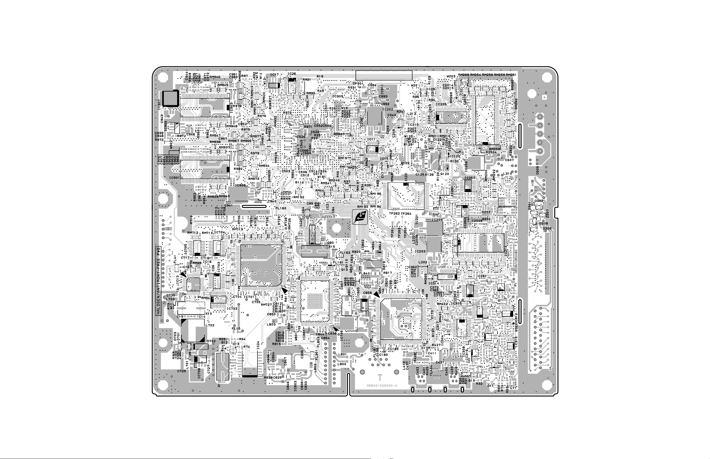
SIGNAL DVD-LCD BOARD PD2222A1 (U101)
BOTTOM (FOIL) SIDE
-
25
- -
26
-
Page 26
SIGNAL DVD-LCD BOARD PD2222A1 (U101)
TOP (COMPONENT) SIDE
-
27
- -
28
-
Page 27
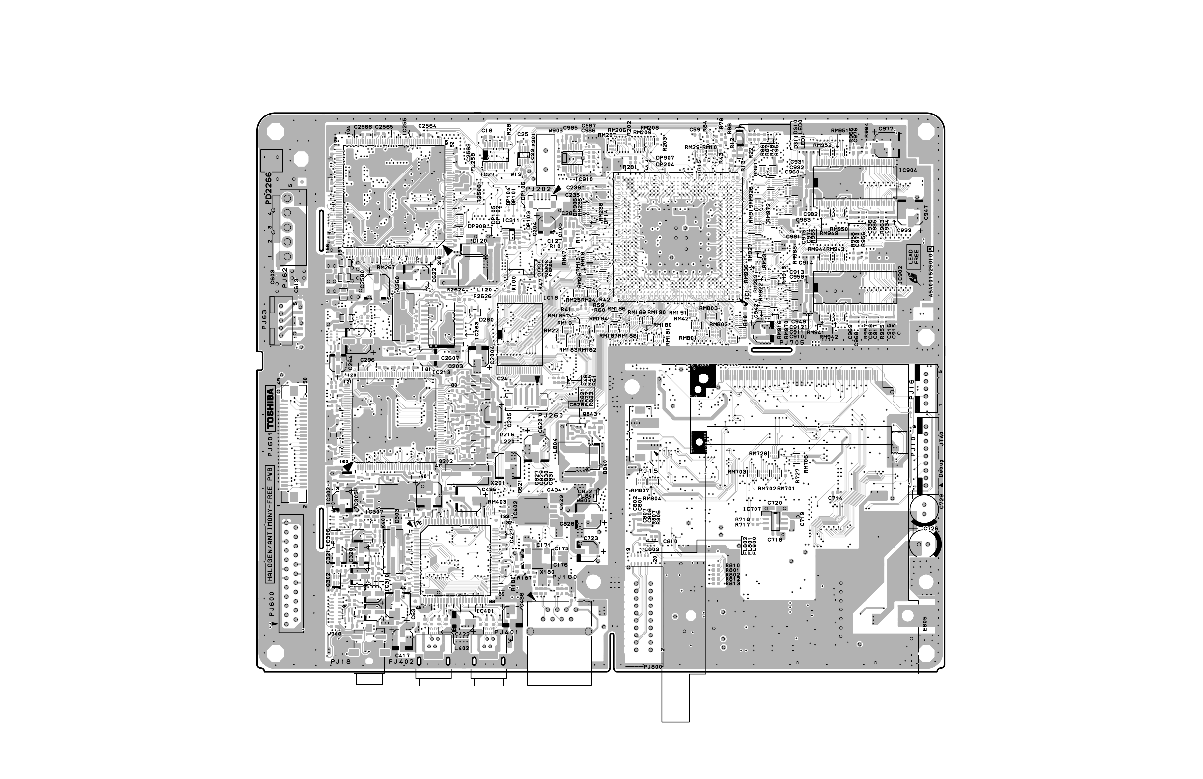
SEINE FOR FPD BOARD PD2266F1 (U102)
BOTTOM (FOIL) SIDE
-
29
- -
30
-
Page 28
SEINE FOR FPD BOARD PD2266F1 (U102)
TOP (COMPONENT) SIDE
-
31
- -
32
-
Page 29
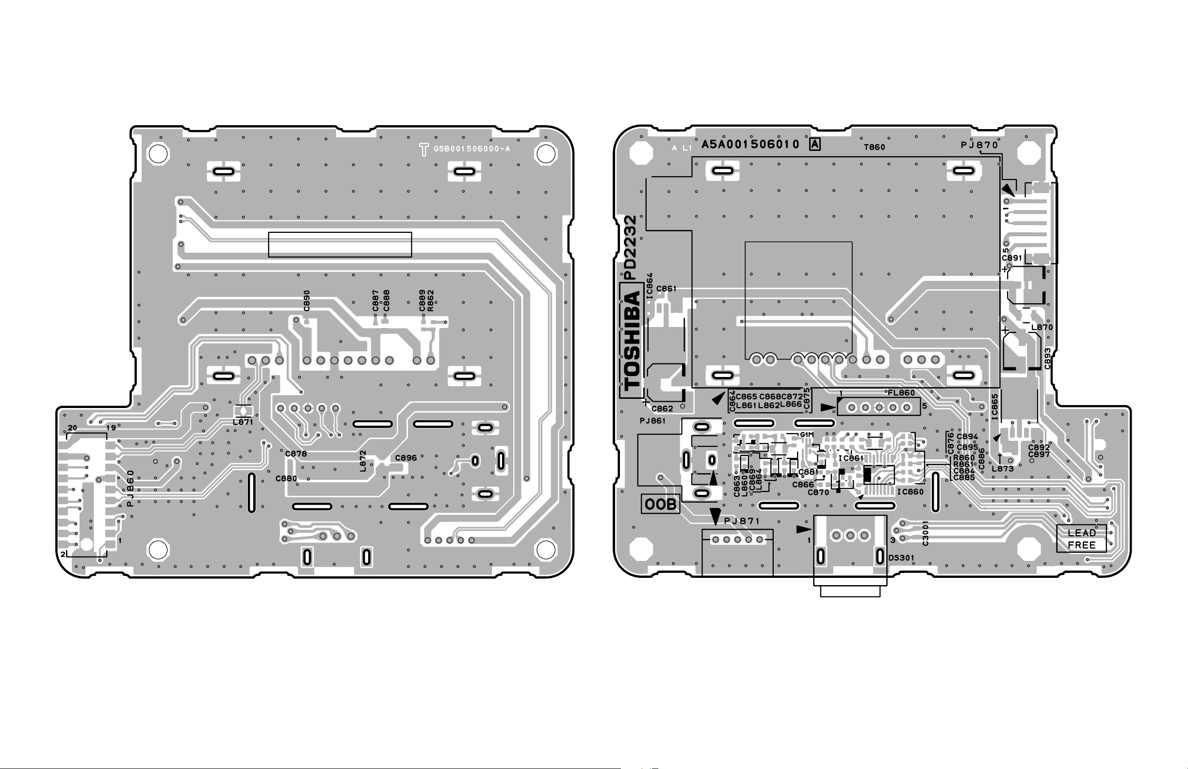
D-TUNER BOARD PD2232A1 (U103)
BOTTOM (FOIL) SIDE
D-TUNER BOARD PD2232A1 (U103)
TOP (COMPONENT) SIDE
-
33
- -
34
-
Page 30
RF-SW TIF BOARD PD2191A1 (U104)
BOTTOM (FOIL) SIDE
OUT
20:NC
C105
20
19
C118
C119
C119
R161
TP-12
L105
R110
C162
PK05
GR02
GR02
16
15
PJ23B
2
1
GR05
GR05
L110
GR03
GR03
GR114
GR114
++
C109
C164
C164 GR04
C118
R165
R165
R110
R161
C162
R168
R168
16:SIF OUT
C161
C161
R167
Q161
R113
R115
Q161
15:NC
C117
R166
R167
GR01
R112
R114
R115
R112
R166
GR01
L101
C114
C115
C114
C115
9
L102
GR04
C116
C117
R114
R113
R105
GR112
GR612
C190
C116
R111
R111
C190
R105
GR112
GR612
L103
L190
L102
L103
R107
R108
L190
R108
R107
Q102
Q102
R103
R103
Q101
R104
Q101
R104
OUT
9:SDA
12:AGC
13:VIDEO
11:AFT
10:SCL
14:GND
17:GND
19:IF
18:5V
4:32V
5:VT
3:GND
6:GND
7:5V
8:AGC
2:NC
1:NC
+++
C107
8
C113
C113
GR113
C104
C102
1
3
D101
D101
C101
C101
C112
GR613
GR613
GR113
C112
C111
C110
C103
C111
C103
C110
H001
C153
DS-7209
23547844
R151
R151
L151
L152
R152
+
C153
C150
GND
SELECT 1
L151
SELECT 2
C152
9V
C152
H003
C151
C151
L152
R152
RF-SW TIF BOARD PD2191A1 (U104)
TOP (COMPONENT) SIDE
OOB
PD2191
H003
23590282A
+
C150
H001
+
+
C104
3
+
C102
8
L101
C107
9
C109
+
+
C105
19 120
L110
TP-12
PK05
L105
15
16
PJ23B
1
2
-
35
-
Page 31

TN/AV-AOUT BOARD PD2217A1 (U105A)
BOTTOM (FOIL) SIDE
GND
5V_DVD
GND
GND
3.3V_DVD
GND
5V_DVDSW
STOP_POD_FAN
STOP_FAN
PD02A
NC
1
DE89
DE90
12V
GND
12V
STOP_FAN
P818
GND
E2
V
RV07
L
RV07
CC07
R
CC08
CC07
CC08
PV16
23547860
DS-7209
Cr
RV26
RV27
RV27
DV03
DV03
B
R6605
C677
R684
D680
R681
C691
C674
C674
D671
D671
D670
D670
R678
R678
Q664
Q665
R6606
R686
D681
D679
C668
R665
R680
C692
R6604
Q671
R6604
+
1
5
+
C671
+
R673
R673
CC03
CC03
C690
+
Q673
D676
R664
D676
C669
C677
R684
R664
C669
D680
R686
R681
R680
C692
Q671
C663
C663
B
D681
C691
R672
Q672
Q672
R676
C670
R676
R675
R671
R671
R675
R677
C661
R677
C667
C665
RL
PV13
CC04
CC04
+
CV74
+
R685
D678
R685
D678
R691
Q673
R6606
C668
R665
D679
R672
C662
C662
R6605
R670
C666
Q665
C664
R6602
R691
GR602
R683
R683
Q660
Q661
Q664
Q661
R690
R6603
R6603
Q663
R6602
Q663
R6601
R6601
+
C660
R670
R674
R674
+
GR602
R692
CV72
V
DV10
RV76
RV76
R692
GR601
GR601
Q660
R690
L
PV14
DV10
CC09
CC09
CS11
R
CC10
CC10
PV97B
2
1
RS18
RS35
CS12
QS05
RS18
RS35
QS05
CS12RS78
RS19
RS19
RS78
RS16
CS10
CS10
CS11
RS16
QS04
QS04
RS20
RS20
RS81
RS17
RS17
QS03
RS81
QS03
L
CC05
CC05
12
13
CS47
CS47
CS46
CS46
CS41
RS41
CS41
RS40
CS40
RS40
CS40
CS52
CS53
CS55
RS55
CS55
RS55
CS56
RS56
CS56
RS56
RV41
RV42
RV42
RV41
R
PV15
CC06
CC06
PV99
2
1
RS47
RS47
RS46
RS46
RS41
RS52
CS52
CS53
RS53
CS81
CS81
RS59
RS58
RS58
RV44
RV43
RV44
RV43
16
15
QS10
CS51
CS50
QS10
CS51
CS50
RS51
RS33
RS50
RS27
RS51
RS50
RS25
RS52
RS60
RS53
CS80
CS80
RS65
RS59
RS66
RS66
QS19
CV63
CV63
QV22
RV61
GR08
RV61
GR08
9V1
5V2
3
19
20
RS31
QS11
RS29
QS11
RS29
RS31
CS15
RS34
QS08
RS61
RS61
RS65
QS19
RS64
RS64
LV31
LV31
QV22
GR07
GR07
PJ21A
1
GND
DE96
RV32
RV32
RV31
RV31
RS32
RS30
RS30
RS32
CS15
RS33
RS28
RS26
RS27
CS16
QS09
RS26
RV60
CV59
CV59
RS34
RS25
QS08
RS60
QS09
LV29
LV30
LV29
LV30
RV62
CV62
RV60
CV61
RV34
CV58
CV60
CV61
RV34
CV58
PD05A
RV33
RV33
RS28
RV62
CV60
NC
GNDNCGND
LOAD_SW
12
A
RD59
CD43
CD67
RD41
RD62
2
1
2
RD61
RD61
1
CD64
CD64
PJ40A
A
RD59
CD43
CS16
CV62
CD67
RD62
RD41
LV33
GJ002
LV33
GJ002
VFD_CS
CD46
CD46
CV25
CV25
RD55
LD43
VFD_CLK
RD55
RD54
GND
NC
DVD_RST
VFD_DATA_IN
VFD_DATA_OUT
PD03A
1
CD41
RD50
RD54
RD56
CD48
CD45
LD40
LD43
LD41
RD45
RD45
LD65
LD65
9
RD50
CD45
RD56
CD48
CD41
LD40
LD41
CV26
CV26
RD22
CD22
PV11
DD11
L
CC01
CC01
S
RV20
DV05
RV20
DV05
RV18
CV10
RV19
8
RV18
CD23
CV10
RV19
1
QD21
24
V
RV21
RV21
CD21
+
+
5
RD21
QD21A
QE89
CE94
1
CE95
QE89A
CE96
+
3
QE90
CE90
1
CE91
QE90A
CE92
+
3
P820
1
RE27
RE27
RE26
RE25
RE26
3
RE25
P819
1
D894
GND
R895
R895
3
D896
D896
1
12V
R897
R897
D897
D897
3
QE21A
R894
QE91A
R894
R896
R896
DE97
QE94A
QE21
DE22
1
RE20
DE21
DE21
RE20
3
CE26
+
RE85
RE90
RE90
QE91
1
DE95
DE95
DE91
3
CE93
+
RD12
RD11
Q670A
DE99
RE85
R
E1
CC02
CC02
RD12
RD11
Y
RV25
RV25
DV01
DV01
CD11
+
Cb
PV12
RV26
DV02
DV02
QD32
E
DE98
AC_DETECT
QE97
QE95
C680
RE84
POWER SW
RE93
RE93
RE84
QE95
GND
RE96
QE97
FE99
125V 1.5A
+
C679
18V
GND
RE96
RE98
5
1
RE94
DE99
RE94
3
QE94
+
FE95
125V_2A
12
QE96
C
E
B
RE88
RE88
FE90
125V_2A
RE87
RE87
RE97
R893
D895
R893
D895
3
1
P821
12V
STOP_FAN
GND
B
C684
Q670
C684
12
D675
D675
11
D674
R679
R679
GND
P602A
FE94
5V1
3,4:AUDIO GND
QE98
PJ63A
18V2
18V1
L_AUDIO
R_AUDIO
1,2:AUDIO VCC
RE91
RE91
F_GND
32V
GND
+
1
1
125V_2A
P803B
1
DE94
DE93
D674
C678
C678
RE95
C681
CE87
C679
C682
4
40V
18V
QE98
RE98
DE92
NC
-
36
- -
37
-
Page 32

PD03A
CD61
TN/AV-AOUT BOARD PD2217A1 (U105A)
TOP (COMPONENT) SIDE
E2
R
L
PV16
PD2217 -1
23590300
VFD_DATA_OUT
VFD_DATA_IN
DVD_RST
VFD_CLK
VFD_CS
GND
QV21
RD101
CD94
GND
NC
NC
CD47
RD57
RD57
LD42
RD63
LD64
CD66
CD61
LD64
10
2
9
CD90
CD92
QV21
RV59
RV59
CD89
RD100
1
LD63
CD62
LD62
CD65
LD63
CD62
LD62
CD65
CD93
RD108
RD105
RD102
RD106
LD01
LD01
CV30
CV30
CV29
CV29
GND
1
RD63
CD66
PJ40A
RD103
RD107
QV18
QV18
V
LOAD_SW
NC
12
CD47
LD42
CD63
1
CD63
LD61
LD61
CD42
CD42
LD44
RD51
RD53
LD44
RD51
CD82
CD82
RD84
RD84
RD86
RD86
CD83
QD20
CD87
CD87
RD103
DD81
DD81
RD107
RD88
RD88
RV201
RV201
LV286
LV28 6
GND
9V1
5V2
PJ21A
RD53
CD81
RD83
RD89
CD84
CD88
CD85
RD90
QD20
5
RD101
CD90
CD89
RD100
RD102
CD94
CD92
CD96
CD96
RV205
RV202
LV288
RV202
LV288
RV205
3
1
DE96
RD85
PD05A
14
CD93
8
RD105
RD106
RV200
RV200
RD82
RD108
19
16
20
15
RD43
RD52
RD44
RD52
RD43
RD44
CD81
RD81
RD83
RD81
RD82
RD89
RD85
CD84
CD88
CD83
RD90
CD85
18
CD91
CD91
QS01
19
CS64
CD95
CD95
RV203
RV203
CS64
RV204
RV204
LV287
LV287
PV15
PV99
CS44
CS45
CS45
CS44
RS45
RS44
RS45
RS44
QS01
RS88
RS82
RS88
RS87
RS87
RV47
RV47
105
LR
12
2
1
CS43
CS42
CS42
CS43
RS42
RS43
RS42
RS43
1
RS82
RS54
RS54
RV45
RV46
20
13
R4105
DV45
Q4102
R4106
R4106
Q4102
R4107
R4107
CS57
CS82
CS82
CS54
CS54
PJ22A
30 40
Q4103
R4108
R4109
Q4109
Q4103
R4108
R4109
GJ414
Q4109
GJ414
CS57
36
RV45
RV46
PJ22A
R
L
PV14
PV97B
2
1
DV44
R4100
R4105
DV45
DV44
R4100
R4123
R4123
Q4100
Q4100
R4122
R4102
Q4101
R4122
R4120
R4103
R4104
GJ413
R4121
GJ413
R4121
C168
C169
C169
C168
50
R4101
Q4108
R4120
Q4101
R4104
5
R4101
R4102
R4103
Q4108
CS505
RS505
10 20
CS503
QS102
RS500
CS504
CS501
RS501
CS501
GRS01
CS503
PJ60A
GRS01
RS501
RS506
RS500
CS504
4
1
CS502
QS102
CS502
8
RS507
5
CS505
RS505
GRS02
RS504
RS517
GRS02
RS517
RS504
PJ60A
40
30 50
RS516
RS507
RS516
RS506
V
CV72
Q670A
R
L
PV13
CV74
+
LV43
LV43
GRV76
GRV76
C685
C685
+
C690
QV17
RV78
CV76
RV78
CV76
CV69
QV16
CV69
CV68
QV16
CV68
+
C675
C675
+
C664
+
C661
C666
C665
C670
C667
C660
Cr
Cb
Y
PV12
QV17
RV105
RV105
+
2
1
C671
C673
C673
LV100
LV102
RV104
RV101
RV101
LV102
RV104
+
LV101
RV103
RV100
RV102
CD11
RV102
RV103
RV100
LV100
LV101
RD32
RD32
RD31
RD31
QD32
QD31
B
12
Q670
11
+
R_AUDIO
P602A
P803B
1
1,2:AUDIO VCC
3,4:AUDIO GND
1
L_AUDIO
GND
GND
4
125V_2A
FE94
5V1
40V
C681
RE95
+
CE87
DE92
PJ63A
1
F_GND
18V1
18V2
32V
NC
QD31
E
18V
DE94
DE93
FE99
+
18V
5
1
+
5
C682
GND
125V 1.5A
C680
GND
E1
POWER SW
AC_DETECT
E
3
STOP_FAN
DE98
QE89
1
QE90
1
3
SVL
QD21
PD02A
5V_DVDSW
8
NC
GND
5V_DVD
GND
GND
3.3V_DVD
GND
1
CD23
+
+
1
24
QD21A
QE89A
DE89
QE90A
DE90
1
12V
P820
GND
STOP_POD_FAN
3
1
12V
GND
STOP_FAN
P818
P819
3
1
12V
GND
STOP_FAN
D894
3
R
PV11
QD11
QD11
CD22
RD21
CD21
5
10
CD12
CD12
DD11
6
RD22
CE94
CE95
CE96
+
3
DE97
QE94A
CE26
DE22
DE91
CE90
CE91
CE92
+
QE21
QE21A
1
3
+
QE91
QE91A
1
1
QE94
3
+
125V_2A
FE95
12
C
QE96
FE90
B
125V_2A
RE97
P821
1
GND
12V
CE93
3
+
-
38
- -
39
-
Page 33

LED-RMT BOARD PD2217A2 (U105B)
BOTTOM (FOIL) SIDE
LED-RMT BOARD PD2217A2 (U105B)
TOP (COMPONENT) SIDE
PJ43A
P601
P602B
RB24
RB24
11
PJ41A
RB22
RB22
1
RB15
RB18
RB15
QB07
DB04
RB18
QB07
CB04
QB04
QB04
CB04
RB10
RB10
+
CB05
CB01
+
DB01
CB38
CB38
RB09
RB09
RB08
RB08
DB23
CB02
DB22
+
DB23
DB20
CB03
CB03
DB22
DB20
KB01
GC601
GC601
23547860
DS-7209
1234
4
C694C688
1
C688
C694
R688
R693
P661
1234
R688
P661
KEY-SW BOARD PD2217A3 (U105C)
BOTTOM (FOIL) SIDE
DA12
RA76 RA71
4
3
2
1
RA77
RA77
SA05RA76 SA06 SA04SA08 RA71
SA03
RA72
RA72
SA02
RA73
RA73
SA01
DA12
DS-7209 23547860
RA74
DA11
DA11
RA74
DA13
RA78
DA13
RA78
SA07
RA79
RA79
DA15
1
2
3
PJ42
4
5
6
DA14
7
DA14
8
DA15
P602B
23590300
R693
P601
14
PD2217
CB01
+
CB05
+
KB01
-2
+
CB02
DB01
PC-IN BOARD PD2217A4 (U105D)
BOTTOM (FOIL) SIDE
DR04
DR05
DR05
DR04
PV90
PS15
CC17
CC16
CC16
DS-7209
CC17
RR03 RR02 RR01
RR03 RR02 RR01
DR02
23547860
DR01
DR01
RR06
RR06
PV97A
13
12
DR02
RR05
DR03
DR03
RR05
RR04
RR04
1
2
1
11
++
DB04
PJ41A
PJ42
KEY-SW BOARD PD2217A3 (U105C)
TOP (COMPONENT) SIDE
1
2
3
4
5
6
7
8
POWER
CH-UP
CH-DN VOL-UP
SA03SA02SA07 SA01
PD2217
VOL-DN VIDEO/TEXTMENU GUIDE
-3
SA05 SA06SA04 SA08
23590300
4
3
2
1
PJ43A
PC-IN BOARD PD2217A4 (U105D)
TOP (COMPONENT) SIDE
PS15
PV90
23590300
-4PD2217
PV97A
131211109
543
1
7
8
2
6
-
40
- -
41
-
Page 34

DVD-KEY BOARD PD2217A5 (U105E)
BOTTOM (FOIL) SIDE
23547860
SA14
RD78
SA15
RD76
RD76
RD78
RD77
RD77
PJ43
SA11
SA12
DS-7209
RD73
RD74
RD73
SA13
RD74
DVD-KEY BOARD PD2217A5 (U105E)
TOP (COMPONENT) SIDE
-5PD2217
23590300
1
2
3
4
PJ43
PLAY
1
2
SA15
3
4
STOP
SA14
SKIP FWD
SA13
SKIP REV
SA12
EJECT
SA11
-
42
-
Page 35

POWER BOARD PD2237D1 (U801)
BOTTOM (FOIL) SIDE
RE14
DE17
DE12
DE08
CE29
DE19
C822
C826
C827
DE13
RE16
C820
CE23
CE22
C824
+
R814
R812
12
C819
QE01
CE09
D805
R813
R805
R803
D809
Q801A
C817
R806
D810
DE14
DE07
7
DE15
+
C825
R817
D806
R807
1
R815
C815
R808
QE01A
1
RE29
CE17
RE15
Q801
RE18
L803
P812B
1
C821
L804
15
14
D811
D812
R809
DE16
RE17
RE13
CE07
CE12
DE09
RE12
CE10
125V 5A
F802
C810
24
C804
1
+
CE16
LE11
+
FE01
250V F3.15AL
CAUTION
+
CE18
LIVE AREA
+
DE06
RE23
D813
C816
CE21
DE05
LE12
DE11
RE05
P811B
3
RE19
CE15
C803
C823
P890
R821
L805
C813
CE11
TE62
QE26
Q826
T862
R873
R874
C899
DE77A
125V 5A
125V 5A
125V 5A
125V 1A
CE82
DE77
DE72
+
+
FE74
FE73
FE75
FE72
5432
CE85
DE75A
L876
L878
D884A
L875
125V 4A
D885
G
B
DE73A
+
F889
125V 5A
L874
C
C890
DE75
+
CE84
CE83
D884
+
C889
Q883
FE76
DE73
C884
+
LE71
+
QE73
RE74
QE93A
E
QE93
CE43
+
CE86
QE83
P813B
C
4321
B
CE74
DE71
DS-7209
23547873
D883A
D883
CE41
CE73
CE75
L884
C883
+
L890
DE50
QE40
GE50
5
1
CE42
CE40
+
+
LE72
LE52
+
+
LE74
CE76
2
115
12345
PJ62A
R862
R861
L883
L889
L888
LE53
LE73
DE51
CE50
CE51
CE55
PJ80A
16
10
10
P805
P804
1
1
1
P803A
++
12
POWER BOARD PD2237D1 (U801)
TOP (COMPONENT) SIDE
GJ99
R862
10
10
P805
R861
P804
1
1
P803A
1
L888
DE56
DE56
LE73
DE54
DE54
DE52
DE52
+
DE55
DE55
DE51
12
QE75
QE75
RE82
RE82
RE83
RE83
QE74
QE74
QE71
CE51
5
QE71
6
PJ80A
RE51
RE52
RE51
16
RE52
GJ84
C889
Q883
DE73A
D885
RE46
L876
L878
L875
125V 5A
F889
G
C
B
R890
DE73
+
L874
R890
C890
DE75A
+
DE75
CE86
+
GJ841
C883
L883
L889
GJ889
DE50
+
LE53
CE55
CE50
RE58
RE58
RE56
RE57
RE57
CE53
1
CE53
RE59
RE59
RE60
RE60
QE64
QE64
CE52
CE52
CE54
CE54
RE53
RE53
RE55
RE55
RE54
10
RE54
L884
RE79
RE79
QE93
432
QE93A
C
+
+
QE92
P813B
LE71
QE92
D884
D884A
C888
+
C888
FE76
125V 4A
1
QE73
RE74
+
CE83
RE45
E
RE45
RE44
RE46
RE41
RE41
RE44
CE43
RE43
RE43
1
QE83
D883A
L890
GJ82
QE40
RE49
GE50
RE49
16
5
RE73
RE73
CE73
+
+
DE71
2345
CE41
D883
CE75
CE74
QE53
C884
RE78
RE78
RE75
RE75
QE52
QE52
B
QE53
RE92
RE92
PJ62A
+
GE51
GE51
1
CE42
CE40
RE56
+
LE52
LE72
RE61
RE61
+
CE76
LE74
2
115
1
CE84
DE72
CE85
R873
R874
125V 5A
RE42
DE77
125V 5A
125V 1A
RE40
RE42
T862
PD2237
1234
+
CE16
FE01
250V F3.15AL
P812B
CAUTION
23590316
125V 5A
F802
C810
C804
LIVE AREA
+
L803
C803
P890
R
8
2
1
R872
R872
DE77A
C899
125V 5A
FE74
FE73
FE75
RE40
FE72
+
CE82
Q826
R816
R816
RE48
RE48
C813
QE26
CE11
C826
C823
D813
L805
C816
TE62
LE12
CE24
CE24
CE21
DE06
DE05
RE05
+
P811B
+
RE19
RE23
LE11
CE18
CE15
DE11
-1
C825
C827
CE10
R815
RE18
R817
1
Q801
R
808
RE15
C815
D806
RE29
QE01
D805
R805
CE17
R807
1
CE09
12534
C817
Q801A
C822
C824
+
R814
R813
R803
D809
D810
DE07
QE01A
DE15
7
+
CE23
R806
RE16
DE14
CE22
C819
R812
DE13
C821
L804
15
D811
14
D812
C820
DE19
R809
DE16
CE07
CE12
RE12
DE09
RE13
RE17
RE14
DE08
CE29
DE12
DE17
-
43
- -
44
-
Page 36

AC-IN BOARD PD2237D2 (U802)
BOTTOM (FOIL) SIDE
31
1
32
4
42
P811A
P813A
D852
SR81
5
LE06
D801A
L806
L807
D801
C806
5
0
8
C
05
E
C
DE01
1
234
P812A
LE07
RE04
3
0
E
R
DE02
CE02
DE03
CE13
CE14
C812
C811
CAUTION
+
C8100
LIVE AREA
+
C8110
CE04
L801
DS-7209
R827
R828
23547873
T802
T801
D899
C802
L802
F801B
F801
F801A
125V 8A
P805B
C801
R801
P800
12
GAP
R899
D899
R801
T801
P800
R899
C801
AC-IN BOARD PD2237D2 (U802)
TOP (COMPONENT) SIDE
Q851
D852
Q851
Q852
Q852
R853
R853
R854
R854
+
PD2237
R850
C852
C852
R858
Q855
R858
Q855
R850
R857
R857
D801A
D801
C806
+
C8110
-2
R827
23590316
T802
DE02
GJ90
GJ88
GJ87
C802
F801B
F801
125V 8A
F801A
21
P805B
GAP
GJ89
C812
C811
L802
CE13
CE14
CE02
AC_IN
RE04
DE03
P812A
1
GJ94
LE07
R
E
0
3
DE01
GJ93
LE06
5
432
SR81
+-
C805
C
E
05
CE04
CAUTION
LIVE AREA
L801
R828
P813A
432
R855
R855
Q854
Q854
R859
R859
L807
GJ91
L806
GJ92
R852
R852
1
R856
Q853
R856
C851
C851
Q853
R851
R851
4321
P811A
C8100
-
45
- -
46
-
Page 37

SCHEMATIC DIAGRAM
MODEL : 27HLV95
WARNING : BEFORE SERVICING THIS CHASSIS, READ THE "SERVICE SAFETY PRECAUTIONS" ON PAGE 3 OF
THIS MANUAL.
CAUTION : The international hazard symbols " " in the schematic diagram and the parts list designate components
which have special characteristics important for safety and should be replaced only with types identical to those in the
original circuit or specified in the parts list. The mounting position of replacements is to be identical with originals. Before
replacing any of these components, read carefully the SERVICE SAFETY PRECAUTIONS on the MANUAL for this
model. Do not degrade the safety of the receiver through improper servicing.
NOTE:
1. RESISTOR Resistance is shown in ohm [K = 1.000, M = 1.000.000]. All resistors are 1/6W and 5%
tolerance carbon resistor, unless otherwise noted as the following marks.
1/2R = Metal or Metal oxide of 1/2 watt 1/2S = Carbon compsistion of 1/2 watt
1RF = Fuse resistor of 1 watt 10W = Cement of 10 watt
K = ±10% G = ±2% F = ± 1%
2. CAPACITOR Unless otherwise noted in schematic, all capacitor values less than 1 are expressed in
?F, and the values more than 1 in pF.
All capacitors are ceramic 50V, unless otherwise noted as the following marks.
Electolytic capacitor Mylar capacitor
3. The parts indicated with " * " have special characteristics, and should be replaced with identical parts only.
4. Voltages read with DIGITAL MULTI-METER from point indicated to chassing ground, using a color bar signal with all
controls at normal, line voltage 220 volts.
5. Waveforms are taken receiving color bar signal with enough sensitivity.
6. Voltage reading shown are nominal values and may vary ±20% except H.V.
-
47
-
Page 38

SCHEMATIC DIAGRAM STRUCTURE:
CONNECTOR ................................................................................................................................................... 1/129
AV TERMINAL ................................................................................................................................................... 2/129
A-OUT ............................................................................................................................................................... 3/129
REGULATOR .................................................................................................................................................... 4/129
EPG-SW ............................................................................................................................................................ 5/129
AUDIO SW ........................................................................................................................................................ 6/129
DVD REGULATOR ........................................................................................................................................... 7/129
DVD OP AMP .................................................................................................................................................... 8/129
KEY ................................................................................................................................................................... 9/129
LED/RMT ........................................................................................................................................................ 10/129
DVD KEY ........................................................................................................................................................ 11/129
PC-HDMI(A) .................................................................................................................................................... 12/129
RF-SW & TIF ................................................................................................................................................... 13/129
CONNECTOR(POWER_BOARD) .................................................................................................................. 14/129
MAIN_POWER(POWER_BOARD) ................................................................................................................. 15/129
SUB_POWER(POWER_BOARD) .................................................................................................................. 16/129
AC-INPUT ....................................................................................................................................................... 17/129
SIGNAL ANALOG IN [SHEET-200] .... 18/129
D IN A [SHEET-300] .... 19/129
D IN B [SHEET-301] .... 20/129
HDMI (Link, I2C) [SHEET-302] .... 21/129
HDMI Rx#2 (Video/Audio) [SHEET-303] .... 22/129
HDMI Rx#3 (PWR,Audio) [SHEET-304] .... 23/129
HDMI AUDIO PLL [SHEET-305] .... 24/129
HDMI AUDIO DAC [SHEET-306].... 25/129
HDMI AUDIO OUT [SHEET-307] .... 26/129
HDMI CONTROLLER [SHEET-308].... 27/129
EEPROM1 [SHEET-309] .... 28/129
EEPROM2 [SHEET-310] .... 29/129
MICRO I/O [SHEET-400] .... 30/129
OCM MEMORY I/F [SHEET-401] .... 31/129
FLASH MEMORY [SHEET-402] .... 32/129
SYNC SEPA [SHEET-403] .... 33/129
E2P OTHER [SHEET-404] .... 34/129
STD-BY MICOR [SHEET-405] .... 35/129
CORTEZ REG 1 [SHEET-406] .... 36/129
CORTEZ REG 2 [SHEET-407] .... 37/129
CORTEZ REG 3 [SHEET-408] .... 38/129
BOOT CONFIG [SHEET-409] .... 39/129
SERVICE CONNECTOR [SHEET-410].... 40/129
I2C Switch [SHEET-411].... 41/129
STBY MICRO for DVD internal [SHEET-412] .... 42/129
DVD 10pin connector [SHEET-413] .... 43/129
I2C Level shift [SHEET-414].... 44/129
AUDIO [SHEET-600] .... 45/129
AUDIO MSP [SHEET-601] .... 46/129
CORTEZ 1 [SHEET-700] .... 47/129
CORTEZ 2 [SHEET-701] .... 48/129
DDR I/F [SHEET-702] .... 49/129
DDR SDRAM [SHEET-703] .... 50/129
DDR TERMINATION [SHEET-704] .... 51/129
DCDC CONV. [SHEET-802].... 52/129
LVDS OUT [SHEET-900].... 53/129
LVDS OUT(SHARP LCD) [SHEET-901].... 54/129
Power Connector and Dimming [SHEET-902] .... 55/129
LVDS Power and Others [SHEET-903].... 56/129
-
48
-
Page 39

SEINE FOR FPD SEINE RESET/CLOCK/TIMER/IRC [SHEET-1].... 57/129
SEINE SLOW BUS [SHEET-2] .... 58/129
SLOW BUS ADDRESS REGISTER [SHEET3] .... 59/129
SEINE IIC/UART [SHEET-4] .... 60/129
SEINE PIO [SHEET-5] .... 61/129
ROM/FLASH [SHEET-6].... 62/129
M-SYSTEM(NANDFLASHROM) [SHEET-7].... 63/129
IR [SHEET-8].... 64/129
GLINK IR-OUT [SHEET-9] .... 65/129
CLOCK GEN. [SHEET-10].... 66/129
USB I/F [SHEET-11].... 67/129
UART0 INTERFACE [SHEET-12].... 68/129
EJTAG CONNECTOR [SHEET-13] .... 69/129
SEINE PCI BUS [SHEET-14].... 70/129
MPU POWER [SHEET-16] .... 71/129
Ext UART [SHEET-17].... 72/129
MACPHYTER 1 (1/2) [SHEET-20].... 73/129
(2/2) [SHEET-21].... 74/129
RJ45 [SHEET-22].... 75/129
TUENR CONNECTOR [SHEET-100] .... 76/129
T313(Signal) [SHEET-101] .... 77/129
1.1VRegulator [SHEET-102].... 78/129
T313(Power) [SHEET-103] .... 79/129
Seine TS I/F [SHEET-150].... 80/129
SEINE CAPTURE IN [SHEET-200] .... 81/129
VIDEO POWER [SHEET-210] .... 82/129
SEINE DIGITAL OUT [SHEET-220].... 83/129
SEINE-BEP IF [SHEET-221] .... 84/129
SEINE DAC OUT [SHEET-225] .... 85/129
DOWN CON OUT DRIVER [SHEET-226] .... 86/129
HD OUT LPF [SHEET-227] .... 87/129
MACRO VCD (1/2) [SHEET-240].... 88/129
(2/2) [SHEET-241].... 89/129
VIDEO LPF [SHEET-242] .... 90/129
MPEG Enc. (CLK, SDRAM) [SHEET-250] .... 91/129
MPEG Enc. (AV I/F) [SHEET-251].... 92/129
MPEG Enc. (STREAM I/F) [SHEET-252] .... 93/129
MPEG Enc. (POWER) [SHEET-253] .... 94/129
LPF, Slicer [SHEET-260] .... 95/129
H/V Sync Sep. [SHEET-261] .... 96/129
AUDIO POWER [SHEET-300] .... 97/129
SEINE AUDIO I/F [SHEET-301] .... 98/129
AUDIO DAC [SHEET-302] .... 99/129
AUDIO PLL/DAC [SHEET-303].. 100/129
AUDIO VTR OUT [SHEET-304].. 101/129
AUDIO SP OUT [SHEET-305] .. 102/129
MPEG2 AUDIO TV IN [SHEET-306] .. 103/129
MPEG2 AUDIO ADC [SHEET-307] .. 104/129
MPEG2 AUDIO PLL [SHEET-308] .. 105/129
AUDIO DAC 0.1CH [SHEET-309].. 106/129
AUDIO VTR OUT [SHEET-310].. 107/129
MB86619 [SHEET-400] .. 108/129
MB86619 (POWER) [SHEET-401].. 109/129
CPLD XILINX [SHEET-700] .. 110/129
SLOWBUS [SHEET-701] .. 111/129
-
49
-
Page 40

SEINE FOR FPD PODVPP [SHEET-702].. 112/129
POD I/F [SHEET-703].. 113/129
PODVCC [SHEET-704].. 114/129
DDR SDRAM I/F [SHEET-901] .. 115/129
DDR 1 [SHEET-902].. 116/129
DDR 2 [SHEET-903].. 117/129
DDR 3 [SHEET-904].. 118/129
DDR 4 [SHEET-905].. 119/129
DDR POWER [SHEET-906] .. 120/129
TERMINATOR [SHEET-907] .. 121/129
VCXO [SHEET-941].. 122/129
SEINE VDD/VSS [SHEET-950] .. 123/129
SIGNAL CONNECTOR [SHEET-960].. 124/129
POWER CONNECTOR [SHEET-961].. 125/129
Signal filter [SHEET-964].. 126/129
D-TUNER TUNER CONNECTOR(TUNER) [SHEET-104].. 127/129
OOB FDC [SHEET-105] .. 128/129
FAT TUNER [SHEET-106] .. 129/129
-
50
-
Page 41

LCD
TV set MODE
MONITOR OUT
(REC OUT)
PANEL
AUDIO
Enc.
MPEG
REC Main
VIDEO
REC out
AudioDAC
2Vpp
Composite
(EPG)
Gemster VBI
Y/Cb/Cr(D)
1Vpp(TV or E1)
IC700
OSD
VBI Data
Processor
V
DCDi
MADi
Video
Scaling
Decoder
Front
Analog
LVDS
BEP
End
2nd
Channel
MUX
Process
Digital
Input A
Digital
Input B
GPIO
Micro-
IR I/F
ADC
processor
CIRCUIT BLOCK DIAGRAM
DIGITAL
ADC
Audio
Digital Tuner POD
(REC OUT)
MONITOR OUT
CS1
CS2
PC in
VIDEO2
digital TV
analog TV
TV set MODE
VIDEO OUTPUT (also for recording)
VIDEO1(V/S)
SIGNAL
-6dB
Y/Pb/Pr
DVD
HDMI
-- picture mute: This TV does not provide.
DVD
Built-in unit
MONI-
MONI-OUT
Analog Tuner
-
51
-
TV1
SW
S1
(REC-OUT)
V1
V2
Y/Pb/Pr_2
Y/Pb/Pr_1
CS-SW
CS1
CS2
R/G/B/HD/VD
PC in
RCV
HDMI
IC300
HDMI_1
HDMI_2
Page 42

Page 43

FILE NO. 023-2006060GR
r
r
SUPPLEMENT
SERVICE MANUAL
Colour Television
27HLV95
The above models are classified as either green products (*1) or non-green products. Green product(s) are
indicated by an underlined serial number. This Service Manual describes replacement parts for green
product(s). When repairing any green product(s), use the parts described in this manual and lead-free solde
(*2).
For (*1) and (*2), see the next page.
Use this Service Manual in conjunction with the original Service Manual (File No. 020-200515) fo
27HLV95.
© TOSHIBA SINGAPORE PTE LTD
Pubished in Singapore Feb. 2005 Green
Page 44

(*1)
r
GREEN PRODUCT PROCUREMENT
The EC is actively promoting the WEEE & RoHS Directives that define standards fo
recycling and reuse of Waste Electrical and Electronic Equipment and for the Restriction
of the use of certain Hazardous Substances. From July 1, 2006, the RoHS Directive will
prohibit any marketing of new products containing restricted substances.
Increasing attention is given to issues related to the global environmental. Toshiba
Corporation recognizes environmental protection as a key management tasks, and is doing
its utmost to enhance and improve the quality and scope of its environmental activities. In
line with this, Toshiba proactively promotes Green Procurement, and seeks to purchase
and use products, parts and materials that have low environmental impacts.
Green procurement of parts is not only confined to manufacture. The same green parts
used in manufacture must also be used as replacement parts.
(* 2 )
LEAD-FREE SOLDER
This product is manufactured using lead-free solder as a part of a movement within the
consumer products industry at large to be environmentally responsible. Lead-free solder
must be used in the servicing and repair of this product.
WARNING
This product is manufactured using lead free solder.
DO NOT USE LEAD BASED SOLDER TO REPAIR THIS PRODUCT!
The melting temperature of lead-free solder is higher than that of leaded solder by 86°F to
104°F (30°C to 40°C). Use of a soldering iron designed for lead-based solders to repair
product made with lead-free solder may result in damage to the component and or PCB
being soldered. Great care should be made to ensure high-quality soldering when servicing
this product especially when soldering large components, through-hole pins, and on PCBs
as the level of heat required to melt lead-free solder is high.
- 2 -
Page 45

N
CHASSIS AND CABINET REPLACEMENT PARTS LIST
o
WARNING: BEFORE SERVICING THIS CHASSIS, READ THE "X-RAY RADIATION PRECAUTION", "SAFETY PRECAUTION" AND
"PRODUCT SAFETY NOTICE" ON PAGE 3 OF THE ORIGINAL SERVICE MANUAL (File No. 063-200467)
CAUTION: The international hazard symbols " " in the schematic diagram and the parts list designate components
which have special characteristics important for safety and should be replaced only with types identical t
those in the original circuit or specified in the parts list. The mounting position of replacements is to be identical with
originals. Before replacing any of these components, read carefully the PRODUCT SAFETY NOTICE. Do not degrade
the safety of the receiver through improper servicing.
NOTICE:
• The part number must be used when ordering parts, in order to assist in processing, be sure to include the
Model number and Description.
• The PC board assembly with mark is no longer available after the end of the production.
• The green parts describes in "G" mark, listed to the left side of the Parts No. item.
Model : 27HLV95
Capacitors............. CD : Ceramic Disk PF : Plastic Film EL : Electrolytic
Resistors............... CF : Carbon Film CC : Carbon Composition MF : Metal Film
MF : Oxide Metal Film VR : Variable Resistor FR : Fusible
Resistor
(All CD and PF capacitors are ±5%, 50V and all resistors, ±5%, 1/6W unless otherwise noted.)
Location
No.
CAPACITOR
C102 76073019 CAPACITOR, ELECTROLYTIC, 10V 470UF M C802 76503512 CAPACITOR, PLASTIC FILM, AC275V 0.22UF M
C103 76109102 CAPACITOR, CERAMIC CHIP, 50V B 1000PF K C803 76503250 CAPACITOR, PLASTIC FILM, 400V 0.22UF M
C104 76073084 CAPACITOR, ELECTROLYTIC, 50V 4.7UF M C804 76214103 CAPACITOR, CERAMIC DISC, 500V B 0.01UF K
C105 76073019 CAPACITOR, ELECTROLYTIC, 10V 470UF M C805 76092281 CAPACITOR, CERAMIC DISC, AC250V E 4700PF
C150 76073041 CAPACITOR, ELECTROLYTIC, 16V 470UF M 3A C806 76092281 CAPACITOR, CERAMIC DISC, AC250V E 4700PF
C151 76109103 CAPACITOR, CERAMIC CHIP, 50V B 0.01UF K C810 76073233 CAPACITOR, ELECTROLYTIC, 200V 560UF M
C152 76109103 CAPACITOR, CERAMIC CHIP, 50V B 0.01UF K C811 76092557 CAPACITOR, CERAMIC DISC, AC250V E 2200PF M
C153 76109103 CAPACITOR, CERAMIC CHIP, 50V B 0.01UF K C811 76092569 CAPACITOR, CERAMIC DISC, AC250V E 2200PF M
C161 76109102 CAPACITOR, CERAMIC CHIP, 50V B 1000PF K C8110 76073233 CAPACITOR, ELECTROLYTIC, 200V 560UF M
C162 76105101 CAPACITOR, CERAMIC CHIP, 50V CH 100PF J C812 76092557 CAPACITOR, CERAMIC DISC, AC250V E 2200PF M
C164 76092730 CAPACITOR, CERAMIC CHIP, 16V B 0.1UF K C812 76092569 CAPACITOR, CERAMIC DISC, AC250V E 2200PF M
C168 76109103 CAPACITOR, CERAMIC CHIP, 50V B 0.01UF K C813 76567334 CAPACITOR, PLASTIC FILM, 50V 0.33UF J
C169 76109103 CAPACITOR, CERAMIC CHIP, 50V B 0.01UF K C813 76503047 CAPACITOR, PLASTIC FILM, 63V 0.33UF J
C2607 76619048 CAPACITOR, ELECTROLYTIC CHIP, 25V 4.7UF M C815 76503049 CAPACITOR, PLASTIC FILM, 63V 0.47UF J
C660 76669479 CAPACITOR, ELECTROLYTIC, 50V 4.7UF M C816 76073183 CAPACITOR, ELECTROLYTIC, 35V 220UF M
C661 76669479 CAPACITOR, ELECTROLYTIC, 50V 4.7UF M C817 76567224 CAPACITOR, PLASTIC FILM, 50V 0.22UF J
C662 76109681 CAPACITOR, CERAMIC CHIP, 50V B 680PF K C819 76214101 CAPACITOR, CERAMIC DISC, 500V B 100PF K
C663 76109681 CAPACITOR, CERAMIC CHIP, 50V B 680PF K C820 76567224 CAPACITOR, PLASTIC FILM, 50V 0.22UF J
C668 76109102 CAPACITOR, CERAMIC CHIP, 50V B 1000PF K C821 76092343 CAPACITOR, CERAMIC DISC, 2KV 680PF K
C669 76109102 CAPACITOR, CERAMIC CHIP, 50V B 1000PF K C822 76092344 CAPACITOR, CERAMIC DISC, 2KV 820PF K
C670 76669100 CAPACITOR, ELECTROLYTIC, 50V 10UF M C823 76092341 CAPACITOR, CERAMIC DISC, 2KV R 470PF K
C671 76669100 CAPACITOR, ELECTROLYTIC, 50V 10UF M C824 76591102 CAPACITOR, PLASTIC FILM, 50V 1000PF J
C673 76619102 CAPACITOR, ELECTROLYTIC CHIP, 16V 47UF M C825 76503053 CAPACITOR, PLASTIC FILM, 63V 1UF J
C674 76092731 CAPACITOR, CERAMIC CHIP, 16V B 1UF K C826 76092341 CAPACITOR, CERAMIC DISC, 2KV R 470PF K
C677 76092731 CAPACITOR, CERAMIC CHIP, 16V B 1UF K C827 76678229 CAPACITOR, ELECTROLYTIC, 200V 2.2UF M
C678 76285104 CAPACITOR, CERAMIC CHIP, 50V B 0.1UF K C851 76092538 CAPACITOR, CERAMIC CHIP, 10V F 1UF Z
C679 76285104 CAPACITOR, CERAMIC CHIP, 50V B 0.1UF K C852 76109102 CAPACITOR, CERAMIC CHIP, 50V B 1000PF K
C680 76073073 CAPACITOR, ELECTROLYTIC, 35V 2200UF M 3A C883 76073193 CAPACITOR, ELECTROLYTIC, 35V 2200UF M
C681 76073073 CAPACITOR, ELECTROLYTIC, 35V 2200UF M 3A C884 76073193 CAPACITOR, ELECTROLYTIC, 35V 2200UF M
C682 76073073 CAPACITOR, ELECTROLYTIC, 35V 2200UF M 3A C888 76105101 CAPACITOR, CERAMIC CHIP, 50V CH 100PF J
C684 76109103 CAPACITOR, CERAMIC CHIP, 50V B 0.01UF K C889 76073094 CAPACITOR, ELECTROLYTIC, 50V 1000UF M
C685 76619113 CAPACITOR, ELECTROLYTIC CHIP, 50V 1UF M C890 76567334 CAPACITOR, PLASTIC FILM, 50V 0.33UF J
C690 76669101 CAPACITOR, ELECTROLYTIC, 50V 100UF M C890 76503047 CAPACITOR, PLASTIC FILM, 63V 0.33UF J
C691 76092463 CAPACITOR, CERAMIC CHIP, 16V B 0.22UF K CB01 76202221 CAPACITOR, ELECTROLYTIC, 10V 220UF M
C692 76092463 CAPACITOR, CERAMIC CHIP, 16V B 0.22UF K CB02 76202221 CAPACITOR, ELECTROLYTIC, 10V 220UF M
C801 76503507 CAPACITOR, PLASTIC FILM, AC275V 0.22UF K CB03 76100104 CAPACITOR, CERAMIC CHIP, 25V F 0.1UF Z
C801 76503002 CAPACITOR, PLASTIC FILM, AC275V 0.22UF M CB04 76100104 CAPACITOR, CERAMIC CHIP, 25V F 0.1UF Z
C801 76503055 CAPACITOR, PLASTIC FILM, AC275V 0.22UF M CB05 76202221 CAPACITOR, ELECTROLYTIC, 10V 220UF M
C801 76503512 CAPACITOR, PLASTIC FILM, AC275V 0.22UF M CB38 76100104 CAPACITOR, CERAMIC CHIP, 25V F 0.1UF Z
C802 76503507 CAPACITOR, PLASTIC FILM, AC275V 0.22UF K CC16 76109102 CAPACITOR, CERAMIC CHIP, 50V B 1000PF K
C802 76503002 CAPACITOR, PLASTIC FILM, AC275V 0.22UF M CC17 76109102 CAPACITOR, CERAMIC CHIP, 50V B 1000PF K
Parts No. Description Location
o.
C802 76503055 CAPACITOR, PLASTIC FILM, AC275V 0.22UF M
Parts No. Description
- 3 -
Page 46

R
Location
N
No.
Parts No. Description Parts No. Description
Location
o.
CD11 76073181 CAPACITOR, ELECTROLYTIC, 35V 56UF M CE87 76669100 CAPACITOR, ELECTROLYTIC, 50V 10UF M
CD21 76666470 CAPACITOR, ELECTORLYTIC, 16V 47UF M CE90 76503047 CAPACITOR, PLASTIC FILM, 63V 0.33UF J
CD22 76539474 CAPACITOR, PLASTIC FILM, 50V 0.47UF J CE91 76503041 CAPACITOR, PLASTIC FILM , 63V 0.1UF J
CD22 76567474 CAPACITOR, PLASTIC FILM, 50V 0.47UF J CE92 76794101 CAPACITOR, ELECTROLYTIC, 16V 100UF M
CD23 76666470 CAPACITOR, ELECTORLYTIC, 16V 47UF M CE94 76503047 CAPACITOR, PLASTIC FILM, 63V 0.33UF J
CD41 76105330 CAPACITOR, CERAMIC CHIP, 50V CH 33PF J CE95 76503041 CAPACITOR, PLASTIC FILM , 63V 0.1UF J
CD42 76105330 CAPACITOR, CERAMIC CHIP, 50V CH 33PF J CE96 76794101 CAPACITOR, ELECTROLYTIC, 16V 100UF M
CD43 76105330 CAPACITOR, CERAMIC CHIP, 50V CH 33PF J CS10 76092628 CAPACITOR, CERAMIC CHIP, 6.3V B 10UF K
CD45 76105330 CAPACITOR, CERAMIC CHIP, 50V CH 33PF J CS11 76092628 CAPACITOR, CERAMIC CHIP, 6.3V B 10UF K
CD46 76105330 CAPACITOR, CERAMIC CHIP, 50V CH 33PF J CS12 76109473 CAPACITOR, CERAMIC CHIP, 25V B 0.047UF K
CD47 76105330 CAPACITOR, CERAMIC CHIP, 50V CH 33PF J CS15 76092628 CAPACITOR, CERAMIC CHIP, 6.3V B 10UF K
CD48 76105330 CAPACITOR, CERAMIC CHIP, 50V CH 33PF J CS16 76092628 CAPACITOR, CERAMIC CHIP, 6.3V B 10UF K
CD61 76105330 CAPACITOR, CERAMIC CHIP, 50V CH 33PF J CS40 76092611 CAPACITOR, CERAMIC CHIP, 6.3V B 2.2UF K
CD62 76105330 CAPACITOR, CERAMIC CHIP, 50V CH 33PF J CS41 76092611 CAPACITOR, CERAMIC CHIP, 6.3V B 2.2UF K
CD63 76105330 CAPACITOR, CERAMIC CHIP, 50V CH 33PF J CS42 76092611 CAPACITOR, CERAMIC CHIP, 6.3V B 2.2UF K
CD64 76105330 CAPACITOR, CERAMIC CHIP, 50V CH 33PF J CS43 76092611 CAPACITOR, CERAMIC CHIP, 6.3V B 2.2UF K
CD65 76105330 CAPACITOR, CERAMIC CHIP, 50V CH 33PF J CS44 76092611 CAPACITOR, CERAMIC CHIP, 6.3V B 2.2UF K
CD66 76105330 CAPACITOR, CERAMIC CHIP, 50V CH 33PF J CS45 76092611 CAPACITOR, CERAMIC CHIP, 6.3V B 2.2UF K
CD67 76105330 CAPACITOR, CERAMIC CHIP, 50V CH 33PF J CS46 76092611 CAPACITOR, CERAMIC CHIP, 6.3V B 2.2UF K
CD81 76619040 CAPACITOR, ELECTROLYTIC CHIP, 16V 10UF M 3A CS47 76092611 CAPACITOR, CERAMIC CHIP, 6.3V B 2.2UF K
CD82 76619040 CAPACITOR, ELECTROLYTIC CHIP, 16V 10UF M 3A CS50 76092611 CAPACITOR, CERAMIC CHIP, 6.3V B 2.2UF K
CD83 76109102 CAPACITOR, CERAMIC CHIP, 50V B 1000PF K CS501 76619100 CAPACITOR, ELECTROLYTIC CHIP, 16V 10UF M
CD84 76109102 CAPACITOR, CERAMIC CHIP, 50V B 1000PF K CS502 76092726 CAPACITOR, CERAMIC CHIP, 10V B 2.2UF K
CD85 76105221 CAPACITOR, CERAMIC CHIP, 50V CH 220PF J CS503 76619100 CAPACITOR, ELECTROLYTIC CHIP, 16V 10UF M
CD87 76092731 CAPACITOR, CERAMIC CHIP, 16V B 1UF K CS504 76105470 CAPACITOR, CERAMIC CHIP, 50V CH 47PF J
CD88 76105221 CAPACITOR, CERAMIC CHIP, 50V CH 220PF J CS505 76105470 CAPACITOR, CERAMIC CHIP, 50V CH 47PF J
CD89 76105221 CAPACITOR, CERAMIC CHIP, 50V CH 220PF J CS51 76092611 CAPACITOR, CERAMIC CHIP, 6.3V B 2.2UF K
CD90 76105221 CAPACITOR, CERAMIC CHIP, 50V CH 220PF J CS52 76092611 CAPACITOR, CERAMIC CHIP, 6.3V B 2.2UF K
CD91 76619040 CAPACITOR, ELECTROLYTIC CHIP, 16V 10UF M 3A CS53 76092611 CAPACITOR, CERAMIC CHIP, 6.3V B 2.2UF K
CD92 76109102 CAPACITOR, CERAMIC CHIP, 50V B 1000PF K CS54 76092611 CAPACITOR, CERAMIC CHIP, 6.3V B 2.2UF K
CD93 76105101 CAPACITOR, CERAMIC CHIP, 50V CH 100PF J CS55 76092611 CAPACITOR, CERAMIC CHIP, 6.3V B 2.2UF K
CD94 76109102 CAPACITOR, CERAMIC CHIP, 50V B 1000PF K CS56 76092611 CAPACITOR, CERAMIC CHIP, 6.3V B 2.2UF K
CD95 76619040 CAPACITOR, ELECTROLYTIC CHIP, 16V 10UF M 3A CS57 76619102 CAPACITOR, ELECTROLYTIC CHIP, 16V 47UF M
CD96 76619040 CAPACITOR, ELECTROLYTIC CHIP, 16V 10UF M 3A CS64 76619101 CAPACITOR, ELECTROLYTIC CHIP, 16V 22UF M
CE04 76092281 CAPACITOR, CERAMIC DISC, AC250V E 4700PF CS82 76092611 CAPACITOR, CERAMIC CHIP, 6.3V B 2.2UF K
CE05 76092281 CAPACITOR, CERAMIC DISC, AC250V E 4700PF CV10 76109102 CAPACITOR, CERAMIC CHIP, 50V B 1000PF K
CE07 76503049 CAPACITOR, PLASTIC FILM, 63V 0.47UF J CV59 76105220 CAPACITOR, CERAMIC CHIP, 50V CH 22PF J
CE09 76668339 CAPACITOR, ELECTROLYTIC, 35V 3.3UF M CV61 76105270 CAPACITOR, CERAMIC CHIP, 50V CH 27PF J
CE10 76073217 CAPACITOR, ELECTROLYTIC, 200V 560UF M CV61 76105470 CAPACITOR, CERAMIC CHIP, 50V CH 47PF J
CE12 76503041 CAPACITOR, PLASTIC FILM , 63V 0.1UF J CV62 76105330 CAPACITOR, CERAMIC CHIP, 50V CH 33PF J
CE13 76092561 CAPACITOR, CERA CAP B 250V 101 CD70-B2GA101KYNS CV63 76092730 CAPACITOR, CERAMIC CHIP, 16V B 0.1UF K
CE13 76092549 CAPACITOR, CERA CAP B 250V 101 DE1B3KX101KB5B CV68 76092621 CAPACITOR, CERAMIC CHIP, 10V B 1UF K
CE14 76092561 CAPACITOR, CERA CAP B 250V 101 CD70-B2GA101KYNS CV69 76092621 CAPACITOR, CERAMIC CHIP, 10V B 1UF K
CE14 76092549 CAPACITOR, CERA CAP B 250V 101 DE1B3KX101KB5B CV72 76794471 CAPACITOR, ELECTROLYTIC, 16V 470UF M
CE15 76092337 CAPACITOR, CERAMIC DISC, 2KV 220PF K CV74 76666101 CAPACITOR, ELECTROLYTIC, 16V 100UF M 3A
CE16 76073181 CAPACITOR, ELECTROLYTIC, 35V 56UF M CV76 76100104 CAPACITOR, CERAMIC CHIP, 25V F 0.1UF Z
CE17 76092339 CAPACITOR, CERAMIC DISC, 2KV 330PF K
CE18 76503253 CAPACITOR, PLASTIC FILM, 1250VH 0.01UF H
ESISTOR
CE23 76214471 CAPACITOR, CERAMIC DISC, 500V B 470PF K GE51 76000445 RESISTOR, CHIP JUMPER, 1608TYPE
CE24 76285104 CAPACITOR, CERAMIC CHIP, 50V B 0.1UF K GJ413 76000445 RESISTOR, CHIP JUMPER, 1608TYPE
CE26 76795101 CAPACITOR, ELECTROLYTIC, 25V 100UF M GJ414 76000445 RESISTOR, CHIP JUMPER, 1608TYPE
CE29 76436331 CAPACITOR, CERAMIC DISC, 50V SL 330PF J GR02 76000445 RESISTOR, CHIP JUMPER, 1608TYPE
CE40 76073183 CAPACITOR, ELECTROLYTIC, 35V 220UF M GR03 76000445 RESISTOR, CHIP JUMPER, 1608TYPE
CE42 76539104 CAPACITOR, PLASTIC FILM, 50V 0.1UF J GR04 76000445 RESISTOR, CHIP JUMPER, 1608TYPE
CE43 76503041 CAPACITOR, PLASTIC FILM , 63V 0.1UF J GR05 76000445 RESISTOR, CHIP JUMPER, 1608TYPE
CE43 76539104 CAPACITOR, PLASTIC FILM, 50V 0.1UF J GR112 76000445 RESISTOR, CHIP JUMPER, 1608TYPE
CE43 76567104 CAPACITOR, PLASTIC FILM, 50V 0.1UF J GR113 76000445 RESISTOR, CHIP JUMPER, 1608TYPE
CE51 76617023 CAPACITOR, ELECTROLYTIC, 16V 330UF M GR114 76000445 RESISTOR, CHIP JUMPER, 1608TYPE
CE52 76092179 CAPACITOR, CERAMIC CHIP, 25V B 0.22UF K GR601 76000445 RESISTOR, CHIP JUMPER, 1608TYPE
CE53 76092179 CAPACITOR, CERAMIC CHIP, 25V B 0.22UF K GR612 76000445 RESISTOR, CHIP JUMPER, 1608TYPE
CE55 76073181 CAPACITOR, ELECTROLYTIC, 35V 56UF M GR613 76000445 RESISTOR, CHIP JUMPER, 1608TYPE
CE73 76073186 CAPACITOR, ELECTROLYTIC, 35V 470UF M R103 76011101 RESISTOR, CHIP, 1/20W 100 OHM J
CE74 76073189 CAPACITOR, ELECTROLYTIC, 35V 1000UF M R104 76011103 RESISTOR, CHIP, 1/20W 10K OHM J
CE75 76073128 CAPACITOR, ELECTROLYTIC, 6.3V 1000UF M R105 76011273 RESISTOR, CHIP, 1/20W 27K OHM J
CE76 76073181 CAPACITOR, ELECTROLYTIC, 35V 56UF M R107 76000445 RESISTOR, CHIP JUMPER, 1608TYPE
CE82 76676470 CAPACITOR, ELECTROLYTIC, 100V 47UF M R108 76000445 RESISTOR, CHIP JUMPER, 1608TYPE
CE83 76073175 CAPACITOR, ELECTROLYTIC, 25V 1800UF M R110 76011682 RESISTOR, CHIP, 1/20W 6.8K OHM J
CE84 76073178 CAPACITOR, ELECTROLYTIC, 25V 3300UF M R114 76000445 RESISTOR, CHIP JUMPER, 1608TYPE
CE85 76073190 CAPACITOR, ELECTROLYTIC CE04P 35V 1200UF M 3A R161 76011102 RESISTOR, CHIP, 1/20W 1K OHM J
CE86 76073190 CAPACITOR, ELECTROLYTIC CE04P 35V 1200UF M 3A R165 76011392 RESISTOR, CHIP, 1/20W 3.9K OHM J
- 4 -
Page 47

Location
No.
Parts No. Description Parts No. Description
Location
No.
R166 76011472 RESISTOR, CHIP, 1/20W 4.7K OHM J RA71 76011683 RESISTOR, CHIP, 1/20W 68K OHM J
R167 76011101 RESISTOR, CHIP, 1/20W 100 OHM J RA72 76011223 RESISTOR, CHIP, 1/20W 22K OHM J
R168 76011101 RESISTOR, CHIP, 1/20W 100 OHM J RA73 76011103 RESISTOR, CHIP, 1/20W 10K OHM J
R4100 76011102 RESISTOR, CHIP, 1/20W 1K OHM J RA74 76000445 RESISTOR, CHIP JUMPER, 1608TYPE
R4101 76011681 RESISTOR, CHIP, 1/20W 680 OHM J RA76 76011223 RESISTOR, CHIP, 1/20W 22K OHM J
R4102 76011471 RESISTOR, CHIP, 1/20W 470 OHM J RA77 76011103 RESISTOR, CHIP, 1/20W 10K OHM J
R4103 76011102 RESISTOR, CHIP, 1/20W 1K OHM J RA78 76000445 RESISTOR, CHIP JUMPER, 1608TYPE
R4104 76011152 RESISTOR, CHIP, 1/20W 1.5K OHM J RA79 76000445 RESISTOR, CHIP JUMPER, 1608TYPE
R4105 76011102 RESISTOR, CHIP, 1/20W 1K OHM J RB08 76011470 RESISTOR, CHIP, 1/20W 47 OHM J
R4106 76011681 RESISTOR, CHIP, 1/20W 680 OHM J RB09 76011470 RESISTOR, CHIP, 1/20W 47 OHM J
R4107 76011471 RESISTOR, CHIP, 1/20W 470 OHM J RB10 76011222 RESISTOR, CHIP, 1/20W 2.2K OHM J
R4108 76011102 RESISTOR, CHIP, 1/20W 1K OHM J RB15 76011471 RESISTOR, CHIP, 1/20W 470 OHM J
R4109 76011152 RESISTOR, CHIP, 1/20W 1.5K OHM J RB24 76000445 RESISTOR, CHIP JUMPER, 1608TYPE
R4120 76000445 RESISTOR, CHIP JUMPER, 1608TYPE RD100 76011562 RESISTOR, CHIP, 1/20W 5.6K OHM J
R4122 76000445 RESISTOR, CHIP JUMPER, 1608TYPE RD101 76011102 RESISTOR, CHIP, 1/20W 1K OHM J
R6601 76011223 RESISTOR, CHIP, 1/20W 22K OHM J RD102 76011562 RESISTOR, CHIP, 1/20W 5.6K OHM J
R6602 76011472 RESISTOR, CHIP, 1/20W 4.7K OHM J RD103 76011562 RESISTOR, CHIP, 1/20W 5.6K OHM J
R6603 76011223 RESISTOR, CHIP, 1/20W 22K OHM J RD105 76011471 RESISTOR, CHIP, 1/20W 470 OHM J
R6604 76011102 RESISTOR, CHIP, 1/20W 1K OHM J RD106 76011562 RESISTOR, CHIP, 1/20W 5.6K OHM J
R6605 76011103 RESISTOR, CHIP, 1/20W 10K OHM J RD107 76011562 RESISTOR, CHIP, 1/20W 5.6K OHM J
R6606 76011104 RESISTOR, CHIP, 1/20W 100K OHM J RD11 76011393 RESISTOR, CHIP, 1/20W 39K OHM J
R664 76011104 RESISTOR, CHIP, 1/20W 100K OHM J RD12 76011152 RESISTOR, CHIP, 1/20W 1.5K OHM J
R665 76011104 RESISTOR, CHIP, 1/20W 100K OHM J RD21 76367101 RESISTOR, CARBON FILM, 1/6W 100 OHM G
R670 76011472 RESISTOR, CHIP, 1/20W 4.7K OHM J RD22 76367222 RESISTOR, CARBON FILM, 1/6W 2.2K OHM G
R671 76011472 RESISTOR, CHIP, 1/20W 4.7K OHM J RD31 76011153 RESISTOR, CHIP, 1/2OW 15K OHM J
R672 76011182 RESISTOR, CHIP, 1/20W 1.8K OHM J RD32 76011473 RESISTOR, CHIP, 1/20W 47K OHM J
R673 76011182 RESISTOR, CHIP, 1/20W 1.8K OHM J RD41 76011101 RESISTOR, CHIP, 1/20W 100 OHM J
R678 76871229 RESISTOR, CHIP, 1/8W 2.2 OHM J RD43 76000445 RESISTOR, CHIP JUMPER, 1608TYPE
R679 76871229 RESISTOR, CHIP, 1/8W 2.2 OHM J RD44 76000445 RESISTOR, CHIP JUMPER, 1608TYPE
R680 76011473 RESISTOR, CHIP, 1/20W 47K OHM J RD45 76011101 RESISTOR, CHIP, 1/20W 100 OHM J
R681 76011473 RESISTOR, CHIP, 1/20W 47K OHM J RD50 76000445 RESISTOR, CHIP JUMPER, 1608TYPE
R683 76011223 RESISTOR, CHIP, 1/20W 22K OHM J RD51 76000445 RESISTOR, CHIP JUMPER, 1608TYPE
R684 76011104 RESISTOR, CHIP, 1/20W 100K OHM J RD52 76000445 RESISTOR, CHIP JUMPER, 1608TYPE
R685 76011183 RESISTOR, CHIP, 1/20W 18K OHM J RD53 76000445 RESISTOR, CHIP JUMPER, 1608TYPE
R686 76011102 RESISTOR, CHIP, 1/20W 1K OHM J RD54 76000445 RESISTOR, CHIP JUMPER, 1608TYPE
R688 76552331 RESISTOR, OXIDE METAL FILM, 1/2W 330 OHM J RD55 76000445 RESISTOR, CHIP JUMPER, 1608TYPE
R691 76000445 RESISTOR, CHIP JUMPER, 1608TYPE RD56 76000445 RESISTOR, CHIP JUMPER, 1608TYPE
R693 76552331 RESISTOR, OXIDE METAL FILM, 1/2W 330 OHM J RD57 76000445 RESISTOR, CHIP JUMPER, 1608TYPE
R801 76009954 RESISTOR, METAL FILN, 1/2W 2.2M OHM J RD59 76000445 RESISTOR, CHIP JUMPER, 1608TYPE
R801 76004716 RESISTOR, METAL GLAZE, 1/2W 2.2M OHM J RD61 76011101 RESISTOR, CHIP, 1/20W 100 OHM J
R803 76366182 RESISTOR, CARBON FILM, 1/6W 1.8K OHM J RD62 76011101 RESISTOR, CHIP, 1/20W 100 OHM J
R805 76366102 RESISTOR, CARBON FILM, 1/6W 1K OHM J RD63 76011101 RESISTOR, CHIP, 1/20W 100 OHM J
R806 76552470 RESISTOR, OXIDE METAL FILM, 1/2W 47 OHM J RD73 76011153 RESISTOR, CHIP, 1/2OW 15K OHM J
R807 76366153 RESISTOR, CARBON FILM, 1/6W 15K OHM J RD74 76000445 RESISTOR, CHIP JUMPER, 1608TYPE
R808 76552101 RESISTOR, OXIDE METAL FILM, 1/2W 100 OHM J RD76 76011563 RESISTOR, CHIP, 1/20W 56K OHM J
R809 76321689 RESISTOR, OXIDE METAL FILM, 1/2W 6.8 OHM J RD77 76011153 RESISTOR, CHIP, 1/2OW 15K OHM J
R812 76552681 RESISTOR, OXIDE METAL FILM, 1/2W 680 OHM J RD78 76000445 RESISTOR, CHIP JUMPER, 1608TYPE
R813 76366120 RESISTOR, CARBON FILM, 1/6W 12 OHM J RD82 76011471 RESISTOR, CHIP, 1/20W 470 OHM J
R814 76552330 RESISTOR, OXIDE METAL FILM, 1/2W 33 OHM J RD83 76011562 RESISTOR, CHIP, 1/20W 5.6K OHM J
R815 76552100 RESISTOR, OXIDE METAL FILM, 1/2W 10 OHM J RD84 76011562 RESISTOR, CHIP, 1/20W 5.6K OHM J
R816 76011681 RESISTOR, CHIP, 1/20W 680 OHM J RD85 76011562 RESISTOR, CHIP, 1/20W 5.6K OHM J
R817 76382823 RESISTOR, OXIDE METAL FILM, 1W 82K OHM J RD86 76011562 RESISTOR, CHIP, 1/20W 5.6K OHM J
R821 76382680 RESISTOR, OXIDE METAL FILM, 1W 68 OHM J RD88 76011222 RESISTOR, CHIP, 1/20W 2.2K OHM J
R827 76383103 RESISTOR, OXIDE METAL FILM, 2W 10K OHM J RD89 76011562 RESISTOR, CHIP, 1/20W 5.6K OHM J
R850 76011101 RESISTOR, CHIP, 1/20W 100 OHM J RD90 76011102 RESISTOR, CHIP, 1/20W 1K OHM J
R851 76011102 RESISTOR, CHIP, 1/20W 1K OHM J RE03 76553683 RESISTOR, OXIDE METAL FILM, 1W 68K OHM J
R852 76011471 RESISTOR, CHIP, 1/20W 470 OHM J RE04 76553683 RESISTOR, OXIDE METAL FILM, 1W 68K OHM J
R853 76011103 RESISTOR, CHIP, 1/20W 10K OHM J RE05 76554683 RESISTOR, OXIDE RES 2W 68K J
R854 76011102 RESISTOR, CHIP, 1/20W 1K OHM J RE12 76552221 RESISTOR, OXIDE METAL FILM, 1/2W 220 OHM J
R855 76011471 RESISTOR, CHIP, 1/20W 470 OHM J RE13 76366473 RESISTOR, CARBON FILM, 1/6W 47K OHM J
R856 76011102 RESISTOR, CHIP, 1/20W 1K OHM J RE15 76366102 RESISTOR, CARBON FILM, 1/6W 1K OHM J
R857 76011471 RESISTOR, CHIP, 1/20W 470 OHM J RE16 76366102 RESISTOR, CARBON FILM, 1/6W 1K OHM J
R858 76011471 RESISTOR, CHIP, 1/20W 470 OHM J RE17 76366363 RESISTOR, CARBON FILM, 1/6W 36K OHM J
R859 76011102 RESISTOR, CHIP, 1/20W 1K OHM J RE18 76019463 RESISTOR, METAL PLATE, 2W 0.22 OHM J
R861 76007416 RESISTOR, CERAMIC COVERED, 5W 82 OHM J RE19 76988022 RESISTOR, METAL FILM, 1/2W 8.2 OHM J
R862 76120002 RESISTOR, CERAMIC COVERED, 5W 68 OHM J RE19 76310829 RESISTOR, OXIDE METAL FILM, 1/2W 8.2 OHM J
R873 76366152 RESISTOR, CARBON FILM, 1/6W 1.5K OHM J RE20 76871152 RESISTOR, CHIP, 1/8W 1.5K OHM J
R890 76011102 RESISTOR, CHIP, 1/20W 1K OHM J RE23 76552152 RESISTOR, OXIDE METAL FILM, 1/2W 1.5K OHM J
R899 76005014 RESISTOR, METAL FILM, 1W 8.2M OHM J RE25 76011103 RESISTOR, CHIP, 1/20W 10K OHM J
R899 76004718 RESISTOR, METAL GLAZE, 1/2W 8.2M OHM J RE26 76011271 RESISTOR, CHIP, 1/20W 270 OHM J
- 5 -
Page 48

Location
No.
Parts No. Description Parts No. Description
Location
No.
RE27 76011472 RESISTOR, CHIP, 1/20W 4.7K OHM J RS51 76011472 RESISTOR, CHIP, 1/20W 4.7K OHM J
RE29 76321828 RESISTOR, METAL FILM, 1/2W 0.82 OHM J RS516 76011101 RESISTOR, CHIP, 1/20W 100 OHM J
RE40 76871681 RESISTOR, CHIP, 1/8W 680 OHM J RS517 76011101 RESISTOR, CHIP, 1/20W 100 OHM J
RE43 76011753 RESISTOR, CHIP, 1/20W 75K OHM J RS52 76011472 RESISTOR, CHIP, 1/20W 4.7K OHM J
RE44 76000593 RESISTOR, METAL FILM CHIP 1/16W 10K F RS53 76011472 RESISTOR, CHIP, 1/20W 4.7K OHM J
RE45 76000445 RESISTOR, CHIP JUMPER, 1608TYPE RS54 76011682 RESISTOR, CHIP, 1/20W 6.8K OHM J
RE46 76000605 RESISTOR, CHIP, 1/16W 6.8K OHM F RS55 76011472 RESISTOR, CHIP, 1/20W 4.7K OHM J
RE48 76011222 RESISTOR, CHIP, 1/20W 2.2K OHM J RS56 76011472 RESISTOR, CHIP, 1/20W 4.7K OHM J
RE51 76011393 RESISTOR, CHIP, 1/20W 39K OHM J RS58 76011101 RESISTOR, CHIP, 1/20W 100 OHM J
RE52 76011152 RESISTOR, CHIP, 1/20W 1.5K OHM J RS59 76011101 RESISTOR, CHIP, 1/20W 100 OHM J
RE53 76871222 RESISTOR, CHIP, 1/8W 2.2K OHM J RS60 76011101 RESISTOR, CHIP, 1/20W 100 OHM J
RE54 76871222 RESISTOR, CHIP, 1/8W 2.2K OHM J RS61 76011101 RESISTOR, CHIP, 1/20W 100 OHM J
RE56 76190012 RESISTOR, METAL FILM CHIP 1/16W 1.5K F RS64 76011682 RESISTOR, CHIP, 1/20W 6.8K OHM J
RE57 76190012 RESISTOR, METAL FILM CHIP 1/16W 1.5K F RS65 76011182 RESISTOR, CHIP, 1/20W 1.8K OHM J
RE58 76190013 RESISTOR, CHIP RES 1/16W 22K F RS66 76011100 RESISTOR, CHIP, 1/20W 10 OHM J
RE59 76011334 RESISTOR, CHIP, 1/20W 330K OHM J RS78 76011102 RESISTOR, CHIP, 1/20W 1K OHM J
RE60 76011473 RESISTOR, CHIP, 1/20W 47K OHM J RS81 76011102 RESISTOR, CHIP, 1/20W 1K OHM J
RE61 76190014 RESISTOR, METAL FILM CHIP 1/16W 18K F RS82 76011682 RESISTOR, CHIP, 1/20W 6.8K OHM J
RE73 76011224 RESISTOR, CHIP, 1/20W 220K OHM J RS87 76011101 RESISTOR, CHIP, 1/20W 100 OHM J
RE74 76553680 RESISTOR, OXIDE METAL FILM, 1W 68 OHM J RS88 76011101 RESISTOR, CHIP, 1/20W 100 OHM J
RE78 76011102 RESISTOR, CHIP, 1/20W 1K OHM J RV07 76011750 RESISTOR, CHIP, 1/20W 75 OHM J
RE79 76011473 RESISTOR, CHIP, 1/20W 47K OHM J RV102 76000445 RESISTOR, CHIP JUMPER, 1608TYPE
RE82 76011473 RESISTOR, CHIP, 1/20W 47K OHM J RV103 76000445 RESISTOR, CHIP JUMPER, 1608TYPE
RE83 76011473 RESISTOR, CHIP, 1/20W 47K OHM J RV18 76011750 RESISTOR, CHIP, 1/20W 75 OHM J
RE84 76011152 RESISTOR, CHIP, 1/20W 1.5K OHM J RV19 76011750 RESISTOR, CHIP, 1/20W 75 OHM J
RE87 76011473 RESISTOR, CHIP, 1/20W 47K OHM J RV20 76000445 RESISTOR, CHIP JUMPER, 1608TYPE
RE88 76011103 RESISTOR, CHIP, 1/20W 10K OHM J RV200 76000445 RESISTOR, CHIP JUMPER, 1608TYPE
RE91 76011103 RESISTOR, CHIP, 1/20W 10K OHM J RV201 76000445 RESISTOR, CHIP JUMPER, 1608TYPE
RE92 76011102 RESISTOR, CHIP, 1/20W 1K OHM J RV202 76000445 RESISTOR, CHIP JUMPER, 1608TYPE
RE93 76011223 RESISTOR, CHIP, 1/20W 22K OHM J RV203 76000445 RESISTOR, CHIP JUMPER, 1608TYPE
RE94 76871271 RESISTOR, CHIP, 1/8W 270 OHM J RV204 76000445 RESISTOR, CHIP JUMPER, 1608TYPE
RE95 76553122 RESISTOR, OXIDE METAL FILM, 1W 1.2K OHM J RV205 76000445 RESISTOR, CHIP JUMPER, 1608TYPE
RE96 76011473 RESISTOR, CHIP, 1/20W 47K OHM J RV21 76011750 RESISTOR, CHIP, 1/20W 75 OHM J
RE97 76553681 RESISTOR, OXIDE METAL FILM , 1W 68 OHM J RV25 76011750 RESISTOR, CHIP, 1/20W 75 OHM J
RE98 76011104 RESISTOR, CHIP, 1/20W 100K OHM J RV26 76011750 RESISTOR, CHIP, 1/20W 75 OHM J
RR01 76871750 RESISTOR, CHIP, 1/8W 75 OHM J RV27 76011750 RESISTOR, CHIP, 1/20W 75 OHM J
RR02 76871750 RESISTOR, CHIP, 1/8W 75 OHM J RV31 76011750 RESISTOR, CHIP, 1/20W 75 OHM J
RR03 76871750 RESISTOR, CHIP, 1/8W 75 OHM J RV32 76011750 RESISTOR, CHIP, 1/20W 75 OHM J
RR04 76011330 RESISTOR, CHIP, 1/20W 33 OHM J RV33 76011750 RESISTOR, CHIP, 1/20W 75 OHM J
RR05 76011330 RESISTOR, CHIP, 1/20W 33 OHM J RV34 76011122 RESISTOR, CHIP, 1/20W 1.2K OHM J
RR06 76011330 RESISTOR, CHIP, 1/20W 33 OHM J RV34 76011331 RESISTOR, CHIP, 1/20W 330 OHM J
RS16 76011473 RESISTOR, CHIP, 1/20W 47K OHM J RV41 76000445 RESISTOR, CHIP JUMPER, 1608TYPE
RS17 76011473 RESISTOR, CHIP, 1/20W 47K OHM J RV42 76000445 RESISTOR, CHIP JUMPER, 1608TYPE
RS18 76011103 RESISTOR, CHIP, 1/20W 10K OHM J RV43 76000445 RESISTOR, CHIP JUMPER, 1608TYPE
RS19 76011104 RESISTOR, CHIP, 1/20W 100K OHM J RV44 76000445 RESISTOR, CHIP JUMPER, 1608TYPE
RS20 76011104 RESISTOR, CHIP, 1/20W 100K OHM J RV45 76011750 RESISTOR, CHIP, 1/20W 75 OHM J
RS25 76011101 RESISTOR, CHIP, 1/20W 100 OHM J RV46 76011750 RESISTOR, CHIP, 1/20W 75 OHM J
RS26 76011101 RESISTOR, CHIP, 1/20W 100 OHM J RV61 76011222 RESISTOR, CHIP, 1/20W 2.2K OHM J
RS27 76011222 RESISTOR, CHIP, 1/20W 2.2K OHM J RV62 76011391 RESISTOR, CHIP, 1/20W 390 OHM J
RS28 76011222 RESISTOR, CHIP, 1/20W 2.2K OHM J RV62 76011471 RESISTOR, CHIP, 1/20W 470 OHM J
RS29 76011102 RESISTOR, CHIP, 1/20W 1K OHM J RV76 76011750 RESISTOR, CHIP, 1/20W 75 OHM J
RS30 76011102 RESISTOR, CHIP, 1/20W 1K OHM J RV78 76011123 RESISTOR, CHIP, 1/20W 12K OHM J
RS31 76011104 RESISTOR, CHIP, 1/20W 100K OHM J
RS32 76011104 RESISTOR, CHIP, 1/20W 100K OHM J COILS & TRANSFORMERS
RS33 76011473 RESISTOR, CHIP, 1/20W 47K OHM J LV31 23246662 COIL, CHIP, TRF4100CN
RS34 76011473 RESISTOR, CHIP, 1/20W 47K OHM J LV29 23246654 COIL, CHIP, TRF4220CG
RS35 76011104 RESISTOR, CHIP, 1/20W 100K OHM J L888 23248387 COIL, CHOKE 9X11H 22MMHK 2.5A TLN3499AA
RS40 76011472 RESISTOR, CHIP, 1/20W 4.7K OHM J LE71 23248387 COIL, CHOKE 9X11H 22MMHK 2.5A TLN3499AA
RS41 76011472 RESISTOR, CHIP, 1/20W 4.7K OHM J L101 23248398 COIL, CHOKE, TLN3278D
RS42 76011472 RESISTOR, CHIP, 1/20W 4.7K OHM J LE53 23248453 COIL, CHOKE, TLN3283AI
RS43 76011472 RESISTOR, CHIP, 1/20W 4.7K OHM J LE53 23248399 COIL, CHOKE, TLN3283D
RS44 76011472 RESISTOR, CHIP, 1/20W 4.7K OHM J LE72 23248386 COIL, CHOKE, TLN3481AA
RS45 76011472 RESISTOR, CHIP, 1/20W 4.7K OHM J LE73 23248386 COIL, CHOKE, TLN3481AA
RS46 76011472 RESISTOR, CHIP, 1/20W 4.7K OHM J LE74 23248386 COIL, CHOKE, TLN3481AA
RS47 76011472 RESISTOR, CHIP, 1/20W 4.7K OHM J L806 23248386 COIL, CHOKE, TLN3481AA
RS50 76011472 RESISTOR, CHIP, 1/20W 4.7K OHM J L807 23248386 COIL, CHOKE, TLN3481AA
RS500 76011103 RESISTOR, CHIP, 1/20W 10K OHM J LE72 23248417 COIL, CHOKE, TLN3481AH
RS501 76011153 RESISTOR, CHIP, 1/2OW 15K OHM J LE73 23248417 COIL, CHOKE, TLN3481AH
RS504 76011153 RESISTOR, CHIP, 1/2OW 15K OHM J LE74 23248417 COIL, CHOKE, TLN3481AH
RS505 76011103 RESISTOR, CHIP, 1/20W 10K OHM J L806 23248417 COIL, CHOKE, TLN3481AH
- 6 -
Page 49

Location
No.
Parts No. Description Parts No. Description
Location
No.
L807 23248417 COIL, CHOKE, TLN3481AH D813 23357512 DIODE, AL01Z
L888 23248432 COIL, CHOKE, TLN3499AH D852 23357922 DIODE, 1SS120-7-E
LE71 23248432 COIL, CHOKE, TLN3499AH D852 23357697 DIODE, 1SS133
L883 23248466 COIL, CHOKE, TLN3551AH D883 23362196 DIODE, SCHOTTKY, RB215T-90
T801 23211902 COIL, LINE FILTER, TRF3254AD D884 23362196 DIODE, SCHOTTKY, RB215T-90
LE52 23289025 COIL, PEAKING, TRF4330AT D885 23357408 DIODE, FMX-12S(023-108)
GE50 23103304 FERRITE CHOKE, TEM2011AA DA11 23362042 DIODE, ZENER, UDZS6.8B
GE50 23103302 FERRITE CHOKE, TEM2011AH DA12 23362042 DIODE, ZENER, UDZS6.8B
L805 23103304 FERRITE CHOKE, TEM2011AA DA13 23362042 DIODE, ZENER, UDZS6.8B
L805 23103302 FERRITE CHOKE, TEM2011AH DA14 23362042 DIODE, ZENER, UDZS6.8B
L874 23103304 FERRITE CHOKE, TEM2011AA DA15 23362042 DIODE, ZENER, UDZS6.8B
L874 23103302 FERRITE CHOKE, TEM2011AH DB01 23358606 DIODE, LED RED, SLR-56VC3FPQ
L875 23103304 FERRITE CHOKE, TEM2011AA DB04 23358605 DIODE, LED GREEN, SLR-56MC3FPQR
L875 23103302 FERRITE CHOKE, TEM2011AH DB20 23357406 DIODE, ZENER, UDZS5.6B
L876 23103304 FERRITE CHOKE, TEM2011AA DB22 23357703 DIODE, 1SS355
L876 23103302 FERRITE CHOKE, TEM2011AH DB23 23357703 DIODE, 1SS355
L878 23103304 FERRITE CHOKE, TEM2011AA DD11 23357912 DIODE, ZENER, MTZJ6.2C
L878 23103302 FERRITE CHOKE, TEM2011AH DD81 23357745 DIODE, ZENER, MA8056-M
LE11 23103304 FERRITE CHOKE, TEM2011AA DE01 23362204 DIODE, D3SB60, 7109F08
LE11 23103302 FERRITE CHOKE, TEM2011AH DE02 23357511 DIODE, AG01A
LE12 23103307 FERRITR CHOKE, TEM2014AA DE03 23357511 DIODE, AG01A
LV100 23277002 FERRITE CORE, ACM3225-102-2PT100 DE05 23357104 DIODE, 1SS244
LV102 23277002 FERRITE CORE, ACM3225-102-2PT100 DE06 23357366 DIODE, FR105-B5
ZA01 23103840 FERRITE CORE, TFE1013 DE07 23362103 DIODE, ZENER, DZ33 BS B
ZA02 23103839 FERRITE CORE, TFE1012 DE07 23357900 DIODE, ZENER, MTZJ33B
ZA04 23103914 FERRITE CORE, TFE1015AD DE09 23362074 DIODE, ZENER, DZ6.8 BS B
SR81 23146588 RELAY, DLS5D1-O(M) 0.15W DE09 23357842 DIODE, ZENER, MTZJ6.8B
UF03 23125949 MOTOR, DCFAN12V60MMPOD2 D06R-12TS1001BC1 DE11 23357709 DIODE, RU1P
L802 23217792 TRANSFORMER, CHOKE 1.8MH 4.1A TPW2072AS DE12 23357512 DIODE, AL01Z
L801 23217791 TRANSFORMER, CHOKE 4.8MH 4.1A TPW2071AS DE13 23357512 DIODE, AL01Z
T862 23217804 TRANSFORMER, CONVERTER TPW3562BS DE14 23357512 DIODE, AL01Z
TE62 23217812 TRANSFORMER, CONVERTER TPW3575BS DE15 23362099 DIODE, ZENER, DZ27 BS B
L102 23103828 INDUCTOR, BEAD, TEM2121M DE15 23357892 DIODE, ZENER, MTZJ27B
L103 23103828 INDUCTOR, BEAD, TEM2121M DE16 23357880 DIODE, ZENER, MTZJ20B
L151 23103828 INDUCTOR, BEAD, TEM2121M DE17 23357512 DIODE, AL01Z
L152 23103828 INDUCTOR, BEAD, TEM2121M DE19 23357854 DIODE, ZENER, MTZJ10B
LD01 23103238 INDUCTOR, BEAD, TEM2142AD DE21 23357703 DIODE, 1SS355
LD40 23103230 INDUCTOR, BEAD, TEM2134AD DE21 23362140 DIODE, KDS160-RTK
LD41 23103230 INDUCTOR, BEAD, TEM2134AD DE22 23357866 DIODE, ZENER, MTZJ12C
LD42 23103230 INDUCTOR, BEAD, TEM2134AD DE50 23357706 DIODE, AK04
LD43 23103230 INDUCTOR, BEAD, TEM2134AD DE51 23357842 DIODE, ZENER, MTZJ6.8B
LD44 23103230 INDUCTOR, BEAD, TEM2134AD DE52 23357703 DIODE, 1SS355
LD61 23103230 INDUCTOR, BEAD, TEM2134AD DE52 23362140 DIODE, KDS160-RTK
LD62 23103230 INDUCTOR, BEAD, TEM2134AD DE54 23357703 DIODE, 1SS355
LD63 23103230 INDUCTOR, BEAD, TEM2134AD DE54 23362140 DIODE, KDS160-RTK
LD64 23103230 INDUCTOR, BEAD, TEM2134AD DE55 23357748 DIODE, ZENER, MA8062-M
LD65 23103230 INDUCTOR, BEAD, TEM2134AD DE56 23357800 DIODE, ZENER, MA8300-H
MV97 23389344 FFC, 20706SFWR-P=1.0-L1-13-223 P1.0-13P-230B(WR) DE72 23357366 DIODE, FR105-B5
DE73 23362197 DIODE, SCHOTTKY, RB085T-60
SEMICONDUCTORS DE75 23362205 DIODE, SCHOTTKY VRM90V 10A RB085T-90
D670 23362140 DIODE, KDS160-RTK DE77 23362197 DIODE, SCHOTTKY, RB085T-60
D671 23362140 DIODE, KDS160-RTK DE89 23357866 DIODE, ZENER, MTZJ12C
D674 23362140 DIODE, KDS160-RTK DE90 23357866 DIODE, ZENER, MTZJ12C
D675 23362140 DIODE, KDS160-RTK DE92 23357856 DIODE, ZENER, MTZJ10D
D676 23362140 DIODE, KDS160-RTK DE93 23357861 DIODE, ZENER, MTZJ11A
D678 23362140 DIODE, KDS160-RTK DE94 23357862 DIODE, ZENER, MTZJ11B
D679 23362140 DIODE, KDS160-RTK DE96 23357840 DIODE, ZENER, MTZJ6.2B
D681 23362140 DIODE, KDS160-RTK DE97 23357870 DIODE, ZENER, MTZJ15A
D801 23362200 DIODE, D5SB60, 7009F07 DE98 23357870 DIODE, ZENER, MTZJ15A
D805 23357850 DIODE, ZENER, MTZJ9.1A DE99 23357703 DIODE, 1SS355
D805 23357627 DIODE, ZENER, RD9.1ESA B1 DE99 23362140 DIODE, KDS160-RTK
D806 23357893 DIODE, ZENER, MTZJ27C IC414 23085936 IC, BU4245G-TR
D806 23357666 DIODE, ZENER, RD27ESA B3 IC710 75001217 IC, TC7SH04FU, INVERTER
D809 23357905 DIODE, ZENER, MTZJ36C IC909 75001247 IC, TC7SH32FU(TE85LF)
D809 23357654 DIODE, ZENER, RD36ESA B3 Q670 23085826 IC, 2CH POWER IC HZIP-12P TA8246AHQ(5)
D810 23357893 DIODE, ZENER, MTZJ27C Q670 23085039 IC, TA8246AHQ
D810 23357666 DIODE, ZENER, RD27ESA B3 Q801 23135087 IC, HYBRID VDS=200V STR-Z4317
D811 23357511 DIODE, AG01A Q826 23085431 IC, PHOTO COUPLER, PS2581L1(D)
D812 23357852 DIODE, ZENER, MTZJ9.1C Q826 23000823 IC, PHOTO COUPLER, TLP421F(GR)
D812 23357625 DIODE, ZENER, RD9.1ESA B3 Q883 23135091 IC, SE024N
- 7 -
Page 50

Location
No.
Parts No. Description Parts No. Description
Location
No.
QD11 23135085 IC, CE-1050 LE12 23103330 FILTER, FERRITE CHOKE 3.5X5X2 TEM2014AH
QD20 23085576 IC, OP AMP, BA4558F D899 76000656 VARISTOR, TNR15G471K
QD21 23085396 IC, SI-3033CA(LF1101)
QE01 23135089 IC, STRW6756 MISCELLANEOUS
QE26 23085431 IC, PHOTO COUPLER, PS2581L1(D) F801 23144319 FUSE, CARTRIDGE 5.2X20, 125V 8A
QE26 23000823 IC, PHOTO COUPLER, TLP421F(GR) F801A 23165433 FUSE HOLDER, 5.2
QE40 23085463 IC, SI-8050E F801B 23165433 FUSE HOLDER, 5.2
QE64 23085415 IC, BD4746G F802 23144227 FUSE, CARTRIDGE 5.2X20, 125V 5A
QE71 23135085 IC, CE-1050 F889 23144227 FUSE, CARTRIDGE 5.2X20, 125V 5A
QE73 23135084 IC, MPD6S011S F889 23144715 FUSE, CARTRIDGE 5.2X20, 125V 5A
QE83 23085389 IC, NJM431L FE01 23144380 FUSE, RADIAL LEAD SUB-MINIATUR 250V 3.15A
QE89 23085423 IC, KIA7809API-U/P FE72 23144251 FUSE, AXIAL, 125V 1A
QE90 23085423 IC, KIA7809API-U/P FE72 23144708 FUSE, AXIAL, 125V 1A
QS01 23009916 IC, MM1631AJBE FE73 23144227 FUSE, CARTRIDGE 5.2X20, 125V 5A
QS102 23085576 IC, OP AMP, BA4558F FE73 23144715 FUSE, CARTRIDGE 5.2X20, 125V 5A
QV16 23085823 IC, 2IN-1OUTSW 6DBAMP CLP(PB F MM1508XNRE FE74 23144227 FUSE, CARTRIDGE 5.2X20, 125V 5A
Q101 23205506 TRANSISTOR, 2SC4081 Q FE74 23144715 FUSE, CARTRIDGE 5.2X20, 125V 5A
Q101 23205277 TRANSISTOR, 2SC4116-Y(TE85L,F) FE75 23144227 FUSE, CARTRIDGE 5.2X20, 125V 5A
Q161 23205506 TRANSISTOR, 2SC4081 Q FE75 23144715 FUSE, CARTRIDGE 5.2X20, 125V 5A
Q161 23205277 TRANSISTOR, 2SC4116-Y(TE85L,F) FE76 23144250 FUSE, AXIAL, 125V 4A
Q4100 23085635 TRANSISTOR, 2SC3437-Y(TE85L,F) FE76 23144714 FUSE, AXIAL, 125V 4A
Q4101 23085635 TRANSISTOR, 2SC3437-Y(TE85L,F) FE90 23144710 FUSE, CARTRIDGE 5.2X20, 125V 2A
Q4102 23085635 TRANSISTOR, 2SC3437-Y(TE85L,F) FE94 23144710 FUSE, CARTRIDGE 5.2X20, 125V 2A
Q4103 23085635 TRANSISTOR, 2SC3437-Y(TE85L,F) FE95 23144710 FUSE, CARTRIDGE 5.2X20, 125V 2A
Q663 23205506 TRANSISTOR, 2SC4081 Q FE99 23144709 FUSE, AXIAL 125V 1.5A
Q664 23205506 TRANSISTOR, 2SC4081 Q FE99 23144252 FUSE, AXIAL, 125V 1.5A
Q665 23205325 TRANSISTOR, RN2404(F) PS15 23023469 JACK, PIN JAC 2P 2P JACK
Q671 23205302 TRANSISTOR, 2SC3326-B(F) PV11 23023417 JACK, PIN RA 1S+3/3P
Q672 23205302 TRANSISTOR, 2SC3326-B(F) PV12 23023423 JACK, PIN RA 3P SMK T-4P
Q673 23205443 TRANSISTOR, 2SA1162-Y(F) PV13 23023419 JACK, PIN 2P RA
Q851 23205446 TRANSISTOR, 2SC2412K, Q T146 PV14 23023418 JACK, PIN RA 3/3P
Q852 23205446 TRANSISTOR, 2SC2412K, Q T146 PV15 23023419 JACK, PIN 2P RA
Q853 23205443 TRANSISTOR, 2SA1162-Y(F) PV16 23365563 JACK, PIN 0S3P R_ANG ICE, IJBH4-MYS
Q854 23205446 TRANSISTOR, 2SC2412K, Q T146 MJ22 23389310 CABLE, FFC 0.5 50P L70
Q855 23205446 TRANSISTOR, 2SC2412K, Q T146 MJ60 23389310 CABLE, FFC 0.5 50P L70
QB04 23205463 TRANSISTOR, 2SC2712-Y(TE85L,F) MJ22 23389359 CABLE, FFC 0.5 50P L70 GOLD
QB07 23205463 TRANSISTOR, 2SC2712-Y(TE85L,F) MJ60 23389359 CABLE, FFC 0.5 50P L70 GOLD
QD31 23205446 TRANSISTOR, 2SC2412K, Q T146 MZ01 23513230 CABLE, LVDS30P250MM COM, T4 E30-S30
QD32 23205318 TRANSISTOR, RN1203(F) H003A 23368943 CABLE, PH0NO 350MM JLC YAF11-1194N
QE21 23205442 TRANSISTOR, 2SC3852 H003B 23368943 CABLE, PH0NO 350MM JLC YAF11-1194N
QE21 23205292 TRANSISTOR, 2SD2396 H003 23344525 SWITCH, 2I3O BUNPAI US DIG RSU143
QE52 23205567 TRANSISTOR, CHIP R1=R2=22K SMT RN2403(TE85L,F) SA01 23344505 SWITCH, PUSH 1C1P
QE53 23205330 TRANSISTOR, RN1403(F) SA02 23344505 SWITCH, PUSH 1C1P
QE74 23205330 TRANSISTOR, RN1403(F) SA03 23344505 SWITCH, PUSH 1C1P
QE75 23205446 TRANSISTOR, 2SC2412K, Q T146 SA04 23344505 SWITCH, PUSH 1C1P
QE92 23205446 TRANSISTOR, 2SC2412K, Q T146 SA05 23344505 SWITCH, PUSH 1C1P
QE93 23205301 TRANSISTOR, 2SA1887(FA,F) SA06 23344505 SWITCH, PUSH 1C1P
QE94 23205442 TRANSISTOR, 2SC3852 SA07 23344505 SWITCH, PUSH 1C1P
QE94 23205292 TRANSISTOR, 2SD2396 SA08 23344505 SWITCH, PUSH 1C1P
QE95 23205446 TRANSISTOR, 2SC2412K, Q T146 SA11 23344505 SWITCH, PUSH 1C1P
QE96 23205301 TRANSISTOR, 2SA1887(FA,F) SA12 23344505 SWITCH, PUSH 1C1P
QE97 23205569 TRANSISTOR, CHIP VCEO=120V 2SC2713-GR(TE85L,F SA13 23344505 SWITCH, PUSH 1C1P
QE98 23205568 TRANSISTOR, CHIP VCEO=-120V 2SA1163-GR(TE85L,F SA14 23344505 SWITCH, PUSH 1C1P
QS03 23205302 TRANSISTOR, 2SC3326-B(F) SA15 23344505 SWITCH, PUSH 1C1P
QS04 23205302 TRANSISTOR, 2SC3326-B(F) MV97A 23969797 TAPE
QS05 23205325 TRANSISTOR, RN2404(F) E900A 23965241 TAPE, CC #12 10MM L30M
QS08 23205506 TRANSISTOR, 2SC4081 Q E901A 23965241 TAPE, CC #12 10MM L30M
QS08 23205277 TRANSISTOR, 2SC4116-Y(TE85L,F) P602A 23713937 CONNECTOR, PLUG 4P B4B-PH-K-S(LF)
QS08 23205392 TRANSISTOR, 2SC5343UF-Y(BULK) P602B 23713937 CONNECTOR, PLUG 4P B4B-PH-K-S(LF)
QS08 23205347 TRANSISTOR, KTC4075Y/P P803A 23713944 CONNECTOR, CONNECT B12B-PH-K-S(LF)
QS09 23205506 TRANSISTOR, 2SC4081 Q P803B 23713944 CONNECTOR, CONNECT B12B-PH-K-S(LF)
QS09 23205277 TRANSISTOR, 2SC4116-Y(TE85L,F) P804 23713942 CONNECTOR, 10P, B10B-PH-K-S(LF)
QS09 23205392 TRANSISTOR, 2SC5343UF-Y(BULK) P805 23713942 CONNECTOR, 10P, B10B-PH-K-S(LF)
QS09 23205347 TRANSISTOR, KTC4075Y/P P811A 23713909 CONNECTOR, CONNECTOR B4P-VH(LF)
QS10 23205302 TRANSISTOR, 2SC3326-B(F) P811B 23713909 CONNECTOR, CONNECTOR B4P-VH(LF)
QS11 23205302 TRANSISTOR, 2SC3326-B(F) P812A 23713910 CONNECTOR, CONNECTOR B5P-VH(LF)
QS19 23205506 TRANSISTOR, 2SC4081 Q P812B 23713910 CONNECTOR, CONNECTOR B5P-VH(LF)
QV17 23205329 TRANSISTOR, RN1404(F) P813A 23713937 CONNECTOR, PLUG 4P B4B-PH-K-S(LF)
QV22 23205507 TRANSISTOR, 2SA1576A Q P813B 23713937 CONNECTOR, PLUG 4P B4B-PH-K-S(LF)
X401 75001136 SMD CERAMIC RESONATOR, 8000KHZ PD02A 23713940 CONNECTOR, CONNECT B8B-PH-K-S(LF)
- 8 -
Page 51

Location
No.
Parts No. Description Parts No. Description
Location
No.
PD03A 23713944 CONNECTOR, CONNECT B12B-PH-K-S(LF) A340 23940461 PIECE, PIECE KEY ASSY 27HL95;C045410EG3
PD05A 23757006 CONNECTOR, 20P TOPTYPE B20B-PHDSS(LF) A340 23940461 PIECE, PIECE KEY ASSY 27HL95;C045410EG3
PJ21A 23713934 CONNECTOR, 2MM 3P S WHT, B3B-PH-K-S(LF) A360 23717250 SCREW, PP4X12+SW+W SBN 42HP84;S2681X011
PJ22 23757180 CONNECTOR, FH12-50S-0.5SV(55) FH12-50S-0.5SV(55) A365 23717219 SCREW, PP3X8+SW+W SBN
PJ22 75000442 CONNECTOR, FPC A366 23717216 SCREW, PP4X8+SW+W SBN
PJ22A 23713960 CONNECTOR, 50P FFC 9637S-50Y901 A370 23717267 SCREW, BITTB4X16 SBN
PJ22A 23757176 CONNECTOR, IRS 9637S-50Y902 GLD 9637S-50Y902 A401 23533561 COVER, BACK COVER ASSY 27HLV95
PJ40A 23757001 CONNECTOR, 10P TOPTYPE B10B-PHDSS(LF) A402 23940316 PIECE, PIECE SERVICE 23LC100:C045292E
PJ41 23713943 CONNECTOR, CONNECT B11B-PH-K-S(LF) A410 23717219 SCREW, PP3X8+SW+W SBN
PJ41A 23713943 CONNECTOR, CONNECT B11B-PH-K-S(LF) A420 23436868 FOOT, STAND ASSY 27WL55XE;
PJ42 23713940 CONNECTOR, CONNECT B8B-PH-K-S(LF) A440 23738074 SCREW, PP 5X16 SW+W SBN
PJ43 23713946 CONNECTOR, PLUG 4P S4B-PH-K-S(LF) A445 23533874 COVER, CABLE COVER BOTTOM ASSY 27HLV95;A055169E
PJ43A 23713946 CONNECTOR, PLUG 4P S4B-PH-K-S(LF) A450 23533374 COVER, CABLE COVER SIDE ASSY 27WL55A;A045330E
PJ60 23757180 CONNECTOR, FH12-50S-0.5SV(55) FH12-50S-0.5SV(55) A461 23950113 LABEL, SERIAL NUMBER, TTX3
PJ60 75000442 CONNECTOR, FPC A501 23940477 PIECE, PIECE DVD PANEL ASSY 27HLV95
PJ60A 23713960 CONNECTOR, 50P FFC 9637S-50Y901 A525 23448738 CASE, PIECE DVD BOTTOM 27HLV95 27HLV95;B055059E
PJ60A 23757176 CONNECTOR, IRS 9637S-50Y902 GLD 9637S-50Y902 A540 23717219 SCREW, PP3X8+SW+W SBN
PJ62 23713910 CONNECTOR, CONNECTOR B5P-VH(LF) A545 23717214 SCREW, BITTB3X12SBN
PJ62A 23713910 CONNECTOR, CONNECTOR B5P-VH(LF) A701A 23015147 CARTON, CASE 27HLV95 27HLV95;S1305D064
PJ63A 23713938 CONNECTOR, CONNECT B5B-PH-K-S(LF) A702A 23946986 PACKING, TOP PACKING 27HL85 27HL85;S1304D370
PJ930 23713574 CONNECTOR, 7P TOP TYPE, BM07B-SRSS-TBT(LF) A702B 23946987 PACKING, BOTTOM PACKING 27HL85;S1304D371
PV97A 23757057 CONNECTOR, 13FMN-BTK-A(LF)(SN) 13FMN-BTK-A(LFSN) A702B 23946987 PACKING, BOTTOM PACKING 27HL85;S1304D371
PV97B 23757057 CONNECTOR, 13FMN-BTK-A(LF)(SN) 13FMN-BTK-A(LFSN) A703 23945190 BAG, PROTECTIVE, 26WL36
PP08 23974994 BAND, KESSOKU B255 23717306 SCREW WITH WASHER
PP12 23974994 BAND, KESSOKU B300 23717215 SCREW, PP3X8+SW+W ECO
PP02 23974994 BAND, KESSOKU B310 23717306 SCREW WITH WASHER
BD01 23771573 DVD-LOADER, RL-SL2003 RL-SL2003 B310 23717219 SCREW, PP3X8+SW+W SBN
P661 23023302 EARPHONE JACK B313 23717306 SCREW WITH WASHER
B321 23717214 SCREW, BITTB3X12SBN
TUNER B401 23717225 SCREW, PP4X20+SW+W SBN
H001 23321536 TUNER, TIF US HOR IIC PH 864M ENG36A36GF D801B 23717240 SCREW
D883B 23717240 SCREW
PC BOARD ASSEMBLIES D884B 23717240 SCREW
U104 75001423 PC BOARD ASSY, PD2191A1 RF-SW TIF DE73B 23717240 SCREW
U105A 75001569 PC BOARD ASSY, PD2217A1 TN/AV-AOUT DE75B 23717240 SCREW
U105B 75001570 PC BOARD ASSY, PD2217A2 LED-RMT DE77B 23717240 SCREW
U105C 75001571 PC BOARD ASSY, PD2217A3 KEY-SW E105 23717215 SCREW, PP3X8+SW+W ECO
U105D 75001572 PC BOARD ASSY, PD2217A4 PC-IN E106 23717215 SCREW, PP3X8+SW+W ECO
U105E 75001573 PC BOARD ASSY, PD2217A5 DVD-KEY E871B 23960136 ADHESIVE, SILICONE, TSE3843-W
U101 75001574 PC BOARD ASSY, PD2222A1 SIGNAL DVD-LCD E871B 23960136 ADHESIVE, SILICONE, TSE3843-W
U103 75001408 PC BOARD ASSY, PD2232A1 D-TUNER E910 23717215 SCREW, PP3X8+SW+W ECO
U801 75001575 PC BOARD ASSY, PD2237D1 POWER E911 23717215 SCREW, PP3X8+SW+W ECO
U802 75001576 PC BOARD ASSY, PD2237D2 AC-IN E912 23717215 SCREW, PP3X8+SW+W ECO
U102 75001577 PC BOARD ASSY, PD2266F1 SEIN FOR FPD WITH E913 23717215 SCREW, PP3X8+SW+W ECO
U103 75001699 PC BOARD ASSY, PD2301A1 D-TUNER E914 23717215 SCREW, PP3X8+SW+W ECO
E915 23717215 SCREW, PP3X8+SW+W ECO
LCD PANEL H003C 23747055 NUT, F-CONNECTOR 2H BS
B001 23301641 LCD PANEL MODULE, 04CMO27, V270W1-L04 H003C 23747055 NUT, F-CONNECTOR 2H BS
H003D 23748092 WASHER, WASHER 14.2X9.6X2 32HL95;D055097E
ACCESSORIES H003E 23748093 WASHER, WASHER WAVE15X10.6X0.2 32HL95;D055098E
Y109 23945015 BAG, POLYETHYLENE COVER 250X400 H003F 23748092 WASHER, WASHER 14.2X9.6X2 32HL95;D055097E
Y101 23566697 OWNERS MANUAL, ENG/FRE/SPA 27HLV95 E/F/S PP01 23845859 HOLDER, WIRE, PVC-C0AT, L=70MM
P800 23713702 PLUG, 2P 11.88MM W VT PP07 23528292 HOLDER, ABMM-A-D, (NO SERVICE)
P820 23713754 PLUG, 3P 2.5MM G, B3B-EH-F1-TV4 Q670B 23717240 SCREW
P601 23713755 PLUG, 4P 2.5MM G, B4B-EH-F1-TV4 QD21B 23717241 SCREW, BITTB3X8ECO
P801 23372264 POWER CORD, U/C 125V10A HSV 5 CMC-02P 11111 QE01B 23717240 SCREW
K902 23306630 REMOCON HAND UNIT IR, CTVUSA CT-90236 QE21B 23717241 SCREW, BITTB3X8ECO
K903 23306614 REMOCON IR, BLASTER GLINK 57H93 QE89B 23717241 SCREW, BITTB3X8ECO
K903 23306644 REMOCON IR, IR BLASTER G-LINK VTR CONT.32HL95 QE90B 23717241 SCREW, BITTB3X8ECO
KB01 23009710 REMOCON RECEIVER, GP1UE281RK QE93B 23717240 SCREW
PV90 23713710 SOCKET, D-SUB 15P, KRD-8622 QE94B 23717241 SCREW, BITTB3X8ECO
W661 23351292 SPEAKER, SPK1410AM, 60X120 8-OHM 10W
CABINATE PARTS Y170 23845800 HOLDER, WIRE, NYLON66 D6.8
A201 23533519 COVER, FRONT BEZEL ASSY 27HL95;A045390EG5
A231 23717214 SCREW, BITTB3X12SBN
A231 23738088 SCREW, BTBW3X12ECO
A240 23717267 SCREW, BITTB4X16 SBN
A240 23738085 SCREW, BTB4X12 ECO
A315 23533563 COVER, BACK CENTER COVER 27HLV95
A320 23940386 PIECE, PIECE AV ASSY 27HL85;C045294E
- 9 -
Page 52

TOSHIBA SINGAPORE PTE. LTD.
Blk438B ALEXANDRA ROAD #06-05 ALEXANDRA TECHNOPARK
Page 53

FILE NO. 020-200515
DOCUMENT CREATED IN JAPAN, July, 2005
CIRCUIT DIAGRAMS
SERVICE MANUAL
LCD Color Television
27HLV95
TOSHIBA CORPORATION 2005
-
1
-
Published in Japan, Jul. 2005 (YC)
Page 54

SCHEMATIC DIAGRAM
MODEL : 27HLV95
WARNING : BEFORE SERVICING THIS CHASSIS, READ THE "SERVICE SAFETY PRECAUTIONS" ON THE MANUAL
FOR THIS MODEL.
CAUTION : The international hazard symbols " " in the schematic diagram and the parts list designate components
which have special characteristics important for safety and should be replaced only with types identical to those in the
original circuit or specified in the parts list. The mounting position of replacements is to be identical with originals. Before
replacing any of these components, read carefully the SERVICE SAFETY PRECAUTIONS on the MANUAL for this
model. Do not degrade the safety of the receiver through improper servicing.
NOTE:
1. RESISTOR Resistance is shown in ohm [K = 1.000, M = 1.000.000]. All resistors are 1/6W and 5%
tolerance carbon resistor, unless otherwise noted as the following marks.
1/2R = Metal or Metal oxide of 1/2 watt 1/2S = Carbon compsistion of 1/2 watt
1RF = Fuse resistor of 1 watt 10W = Cement of 10 watt
K = ±10% G = ±2% F = ± 1%
2. CAPACITOR Unless otherwise noted in schematic, all capacitor values less than 1 are expressed in
?F, and the values more than 1 in pF.
All capacitors are ceramic 50V, unless otherwise noted as the following marks.
Electolytic capacitor Mylar capacitor
3. The parts indicated with " * " have special characteristics, and should be replaced with identical parts only.
4. Voltages read with DIGITAL MULTI-METER from point indicated to chassing ground, using a color bar signal with all
controls at normal, line voltage 220 volts.
5. Waveforms are taken receiving color bar signal with enough sensitivity.
6. Voltage reading shown are nominal values and may vary ±20% except H.V.
Page 55

SCHEMATIC DIAGRAM STRUCTURE:
CONNECTOR ................................................................................................................................................... 1/129
AV TERMINAL ................................................................................................................................................... 2/129
A-OUT ............................................................................................................................................................... 3/129
REGULATOR .................................................................................................................................................... 4/129
EPG-SW ............................................................................................................................................................ 5/129
AUDIO SW ........................................................................................................................................................ 6/129
DVD REGULATOR ........................................................................................................................................... 7/129
DVD OP AMP .................................................................................................................................................... 8/129
KEY ................................................................................................................................................................... 9/129
LED/RMT ........................................................................................................................................................ 10/129
DVD KEY ........................................................................................................................................................ 11/129
PC-HDMI(A) .................................................................................................................................................... 12/129
RF-SW & TIF ................................................................................................................................................... 13/129
CONNECTOR(POWER_BOARD) .................................................................................................................. 14/129
MAIN_POWER(POWER_BOARD) ................................................................................................................. 15/129
SUB_POWER(POWER_BOARD) .................................................................................................................. 16/129
AC-INPUT ....................................................................................................................................................... 17/129
SIGNAL ANALOG IN [SHEET-200] .... 18/129
D IN A [SHEET-300] .... 19/129
D IN B [SHEET-301] .... 20/129
HDMI (Link, I2C) [SHEET-302].... 21/129
HDMI Rx#2 (Video/Audio) [SHEET-303] .... 22/129
HDMI Rx#3 (PWR,Audio) [SHEET-304] .... 23/129
HDMI AUDIO PLL [SHEET-305] .... 24/129
HDMI AUDIO DAC [SHEET-306].... 25/129
HDMI AUDIO OUT [SHEET-307] .... 26/129
HDMI CONTROLLER [SHEET-308].... 27/129
EEPROM1 [SHEET-309].... 28/129
EEPROM2 [SHEET-310].... 29/129
MICRO I/O [SHEET-400] .... 30/129
OCM MEMORY I/F [SHEET-401] .... 31/129
FLASH MEMORY [SHEET-402] .... 32/129
SYNC SEPA [SHEET-403] .... 33/129
E2P OTHER [SHEET-404] .... 34/129
STD-BY MICOR [SHEET-405] .... 35/129
CORTEZ REG 1 [SHEET-406] .... 36/129
CORTEZ REG 2 [SHEET-407] .... 37/129
CORTEZ REG 3 [SHEET-408] .... 38/129
BOOT CONFIG [SHEET-409] .... 39/129
SERVICE CONNECTOR [SHEET-410].... 40/129
I2C Switch [SHEET-411].... 41/129
STBY MICRO for DVD internal [SHEET-412] .... 42/129
DVD 10pin connector [SHEET-413] .... 43/129
I2C Level shift [SHEET-414].... 44/129
AUDIO [SHEET-600] .... 45/129
AUDIO MSP [SHEET-601] .... 46/129
CORTEZ 1 [SHEET-700] .... 47/129
CORTEZ 2 [SHEET-701] .... 48/129
DDR I/F [SHEET-702] .... 49/129
DDR SDRAM [SHEET-703] .... 50/129
DDR TERMINATION [SHEET-704] .... 51/129
DCDC CONV. [SHEET-802].... 52/129
LVDS OUT [SHEET-900].... 53/129
LVDS OUT(SHARP LCD) [SHEET-901].... 54/129
Power Connector and Dimming [SHEET-902] .... 55/129
LVDS Power and Others [SHEET-903].... 56/129
Page 56

SEINE FOR FPD SEINE RESET/CLOCK/TIMER/IRC [SHEET-1].... 57/129
SEINE SLOW BUS [SHEET-2] .... 58/129
SLOW BUS ADDRESS REGISTER [SHEET3] .... 59/129
SEINE IIC/UART [SHEET-4] .... 60/129
SEINE PIO [SHEET-5].... 61/129
ROM/FLASH [SHEET-6].... 62/129
M-SYSTEM(NANDFLASHROM) [SHEET-7].... 63/129
IR [SHEET-8].... 64/129
GLINK IR-OUT [SHEET-9] .... 65/129
CLOCK GEN. [SHEET-10].... 66/129
USB I/F [SHEET-11].... 67/129
UART0 INTERFACE [SHEET-12].... 68/129
EJTAG CONNECTOR [SHEET-13] .... 69/129
SEINE PCI BUS [SHEET-14].... 70/129
MPU POWER [SHEET-16] .... 71/129
Ext UART [SHEET-17].... 72/129
MACPHYTER 1 (1/2) [SHEET-20].... 73/129
(2/2) [SHEET-21].... 74/129
RJ45 [SHEET-22].... 75/129
TUENR CONNECTOR [SHEET-100] .... 76/129
T313(Signal) [SHEET-101] .... 77/129
1.1VRegulator [SHEET-102].... 78/129
T313(Power) [SHEET-103] .... 79/129
Seine TS I/F [SHEET-150].... 80/129
SEINE CAPTURE IN [SHEET-200] .... 81/129
VIDEO POWER [SHEET-210] .... 82/129
SEINE DIGITAL OUT [SHEET-220].... 83/129
SEINE-BEP IF [SHEET-221] .... 84/129
SEINE DAC OUT [SHEET-225] .... 85/129
DOWN CON OUT DRIVER [SHEET-226] .... 86/129
HD OUT LPF [SHEET-227] .... 87/129
MACRO VCD (1/2) [SHEET-240].... 88/129
(2/2) [SHEET-241].... 89/129
VIDEO LPF [SHEET-242] .... 90/129
MPEG Enc. (CLK, SDRAM) [SHEET-250] .... 91/129
MPEG Enc. (AV I/F) [SHEET-251].... 92/129
MPEG Enc. (STREAM I/F) [SHEET-252] .... 93/129
MPEG Enc. (POWER) [SHEET-253] .... 94/129
LPF, Slicer [SHEET-260] .... 95/129
H/V Sync Sep. [SHEET-261] .... 96/129
AUDIO POWER [SHEET-300] .... 97/129
SEINE AUDIO I/F [SHEET-301] .... 98/129
AUDIO DAC [SHEET-302] .... 99/129
AUDIO PLL/DAC [SHEET-303].. 100/129
AUDIO VTR OUT [SHEET-304].. 101/129
AUDIO SP OUT [SHEET-305] .. 102/129
MPEG2 AUDIO TV IN [SHEET-306] .. 103/129
MPEG2 AUDIO ADC [SHEET-307] .. 104/129
MPEG2 AUDIO PLL [SHEET-308] .. 105/129
AUDIO DAC 0.1CH [SHEET-309].. 106/129
AUDIO VTR OUT [SHEET-310].. 107/129
MB86619 [SHEET-400] .. 108/129
MB86619 (POWER) [SHEET-401].. 109/129
CPLD XILINX [SHEET-700] .. 110/129
SLOWBUS [SHEET-701] .. 111/129
Page 57

SEINE FOR FPD PODVPP [SHEET-702].. 112/129
POD I/F [SHEET-703].. 113/129
PODVCC [SHEET-704].. 114/129
DDR SDRAM I/F [SHEET-901] .. 115/129
DDR 1 [SHEET-902].. 116/129
DDR 2 [SHEET-903].. 117/129
DDR 3 [SHEET-904].. 118/129
DDR 4 [SHEET-905].. 119/129
DDR POWER [SHEET-906] .. 120/129
TERMINATOR [SHEET-907] .. 121/129
VCXO [SHEET-941].. 122/129
SEINE VDD/VSS [SHEET-950] .. 123/129
SIGNAL CONNECTOR [SHEET-960].. 124/129
POWER CONNECTOR [SHEET-961].. 125/129
Signal filter [SHEET-964].. 126/129
D-TUNER TUNER CONNECTOR(TUNER) [SHEET-104].. 127/129
OOB FDC [SHEET-105] .. 128/129
FAT TUNER [SHEET-106] .. 129/129
Page 58

LCD
TV set MODE
MONITOR OUT
(REC OUT)
PANEL
AUDIO
Enc.
MPEG
REC Main
VIDEO
REC out
AudioDAC
2Vpp
Composite
(EPG)
Gemster VBI
Y/Cb/Cr(D)
1Vpp(TV or E1)
IC700
OSD
VBI Data
Processor
V
DCDi
MADi
Video
Scaling
Decoder
Front
Analog
LVDS
BEP
End
2nd
Channel
MUX
Process
Digital
Input A
Digital
Input B
GPIO
Micro-
IR I/F
ADC
processor
CIRCUIT BLOCK DIAGRAM
DIGITAL
ADC
Audio
Digital Tuner POD
(REC OUT)
MONITOR OUT
CS1
CS2
PC in
VIDEO2
digital TV
analog TV
TV set MODE
VIDEO OUTPUT (also for recording)
VIDEO1(V/S)
SIGNAL
-6dB
Y/Pb/Pr
DVD
HDMI
-- picture mute: This TV does not provide.
DVD
Built-in unit
MONI-
MONI-OUT
Analog Tuner
TV1
SW
S1
(REC-OUT)
V1
V2
Y/Pb/Pr_2
Y/Pb/Pr_1
CS-SW
CS1
CS2
R/G/B/HD/VD
PC in
RCV
HDMI
IC300
HDMI_1
HDMI_2
Page 59

TO SIGNAL BOARD
OTHER PARTS
U121
PWB PD****-1
NV02
SOLDER9025SE
NV03
SOLDER9025SE
NV04
THINNER4520
NV05
FLUX CF330VH
NV06
FLUX CF330VH
NV09
SOLDER9025SE
NV10NV07NV01
THINNER4520SOLDEREX9025SOLDEREX9025
NV11NV08
FLUX CF330VHSOLDER9025SE
RV62
470
V_TV
1-D1,5-B6
GND
TO RFSW-TIF BOARD
PV99
W-B PHD 16P PLUG TOP
426
1
597
3
5V2
32V
GND
GND
9V2
32V
9V2
GND
GND
1-F3,4-A1
TO POD_FAN
P820
PLUG_2.5mm_3P\B3B-EH-F1A
12V
GND
STOP_POD_FAN
3
1
2
RE25
10k
12V_FAN_POD
9V1
1-B1,4-A2,6-B1,8-A1
4-A2
RE26
270
RE27
4.7k
POD_STOP_FAN
1-B5
PJ21A
PLUG_2mm_3P\B3B-PH-K-S
LV30
OPEN
CV62
33p
RV34
1.2k
CV60
CV58
OPEN
OPEN
16P
8
12
10
11
GND
SCL1
SYS_SW1
SYS_SW2
SDA1
5V2
GND
GND
SCL1
SDA1
SYS_SW2
SYS_SW1
1-B8
1-B8
1-B5,6-E1
1-B5,6-E1
1-B2,1-C4,2-C6,5-B5
TO FAN-2
R895
KETSU
D896
KETSU
D894
MTZJ3.3A
VCC_STOP_FAN
4-B1
5V2
9V1
GND
321
5V2
9V1
1-F1,4-A2,6-B1,8-A1
1-C4,1-D1,2-C6,5-B5
LV31
COLTRF4100CN
GR07
LV29
22u
CV61
47p
RV60
OPEN
CV59
22p
16
14
15
13
SIF
GND
GND
AFT1
V_TV
GND
GND
AFT1
V_TV
1-B8
1-B5
1-C1,5-B6
P819
KETSU
STOP_FAN
12V
GND
1
23
12V_FAN
1-F2,1-F2,4-B2
R896
KETSU
R894
KETSU
A1(PR_DVD)
GND
4950 4748 46 45 44 43 42 41 40 39 38 37 36 35 34 33 32 31 30 29 28 27 26 25 2423222120 19 18 17 16 15 14 13 12 11 10 9 8 7 6 5 4 3 2 1
DE96
MTZJ6.2B
GND
PR_DVD
1-D7
OPEN
CV63
RV61
0.1uF
2.2k
GR08
OPEN
QV22
2SA1576A
SIF
TO FAN-1
P818
KETSU
STOP_FAN
3
D897 D895
KETSU KETSU
STOP_FAN
1-B5
SV1(V_E1)
V_E1
2-B3
GND
GND
GND
12
12V_FAN
C1(PB_CS)
PB_CS1
2-B3
12V
1-F2,1-F2,4-B2
SV2(SC_E1)
AN(RET)
B1(NC)
GND
GND
GND
RV41
CHIP_JP
GND
GND
Q4108
KETSU
R4121
KETSU
GND
SC_E1
2-A3
R4103
R4120
Short
GJ413
Short
R4104
1.5k
13P-FFC
PC/HDMI(A)-IN
TO DVD_FAN
P821
KETSU
STOP_FAN
12V
GND
321
R893R897
KETSUKETSU
12V_FAN
1-F2,1-F2,4-B2
A2(NC)
GND
GND
1k
Q4101
2SC3437Y-L
GND
R_HDMI/PC
L_HDMI/PC
GND
V_PC
H_PC
GND
B_PC
GND
G_PC
GND
R_PC
GND
B2(Y_CS)
Y_CS1
2-B3
R4102
GND
R4101
680
470
Q4100
2SC3437Y-L
GND
B_PC
1-D4
PV97B
23FMN-BTK-A
SV3(SY_E1)
RV42
H_PC
R4100
BN(RET)
1k
CHIP_JP
SY_E1
2-A3
PC_HS
GND
R_HDMI1
L_HDMI1
A3(PR_CS)
GND
GND
GND
GND
PR_CS1
2-B3
Q4109
KETSU
GJ414
Short
R4123
KETSU
R_HDMI1
L_HDMI1
GND
GND
B_PC
GND
G_PC
GND
R_PC
GND
C2(B_PC)
13
12
11
10
GND
GND
9
8
7
6
5
4
3
2
1
TO DIGITAL BOARD
NC(LNB)
C3(V_E2)
B3(R_PC)
GND
GND
RV43
GND
GND
V_E2
R_PC
2-E3
1-D4
H_PC
V_PC
R4108
R4122
1k
Short
R4107
Q4103
2SC3437Y-L
R4109
1.5k
GND
6-D1
6-D1
GND
GND
1-B3
B_PC
GND
1-B4
G_PC
GND
1-B3
R_PC
GND
PJ63A
PLUG_2mm_5P\B5B-PH-K-S
18V2(USonly)
18V1
32V
F_GND
45
21
3
125V 1.5A
FE99
32V
18V1
1-D1,4-A1
4-A1,4-A2,7-A1
CN(RET)
CHIP_JP
470
DV44
SV4(V_TV)
R4106
680
DV45
OPEN
GND
Q4102
2SC3437Y-L
OPEN
B4(Y_DVD)
A4(G_PC)
GND
GND
GND
GND
G_PC
Y_DVD
1-D7
1-D4
5V2
1-B2,1-D1,2-C6,5-B5
1k
R4105
VS
CD65
33p
CD66
33p
CD67
33p
50P-FFC 50P-FFC
C4(PB_DVD)
PB_DVD
1-D7
GND(V_DGT)
OPT3(NC)
SNV(RET)
V_DGT
GND
75
RV46
RV45
75
RV44
SHORT
GND
GND
V_DGT
2-C4
DVD
PJ22A
9637S-50ATL\FFC/FPC 0.5mm50P SOCKET
V_EPG(to Seine)
MONI-OUT
OPT9
OPT8
EPG_SW
GND
RV47
OPEN
V_EPG
GND
V_MONI
EPG_SW
5-B2
AFT1
1-D2
2-C4,5-C2
8P
PD02A
GND
3.3V_DVD
GND
GND
5V_DVD
GND
B8B-PH-K-S
5V1
1
GND
2
3.3V_DVD
3
GND
4
GND
5
5V_DVD
6
GND
7
NC
8
5V_DVDSW
DVD
MONI_SW
SW_E1
POD_STOP_FAN
SW_E1
MONI_SW
POD_STOP_FAN
2-D4
2-A3,5-B2
5V1
GND
3.3V_DVD
GND
GND
5V_DVD
GND
PD05A
NC
W-B PHD 20P PLUG TOP
1-F1
1
3
5
7
9
11
13
15
17
19
SDA1
SDA1
1-D2,6-E1
20P
2
4
6
8
10
12
14
16
18
20
SCL1
AFT2
SCL1
1-D2,6-E1
1-C6,7-B2
1-C6,1-C6,1-C6,7-A2
NC
NC
STOP_FAN
STOP_FAN
1-F2
DVD
RD51
RD44
RD53
RD52
RD43
MONI_SW2
CD42
ATXD_cortez
33p
RV33
75
RV32
75
RV31
75
V_PC
H_PC
NC
V_PC
H_PC
1-B4
1-B4
DVD_RST
GND
VFD_DATA_OUT
VFD_CLK 6
VFD_CS 7
GND
LOAD_SW
LD44
120ohm
PDP_CONT_EN
12P
PD03A
10
11
12
B12B-PH-K-S
PDP_MUTE
1
2
3
4
5VFD_DATA_IN
8GND
9
ARXD_cortez
NC
NC
NC
BS_TV_MUTE
SPK_OFF
SPK_OFF
3-B1
CHIP_JP
CHIP_JP
EXT_MUTE
EXT_MUTE
3-B1
CHIP_JP
CHIP_JP
CHIP_JP
CHIP_JP
SPDIF
DVD_L_L
DVD_L_H
DVD_R_H
MUTE
MUTE
3-A1
RD56
DVD_R_L
RD50
RD54
RD55
RD57
RD59
L_HDMI
R_HDMI
L_HDMI
R_HDMI
6-D1
6-D1
CD48
33p
GND
SPDIF
DVD_L_L
DVD_L_H
DVD_R_L
DVD_R_H
L_BS
R_BS
GND
R_DTV
GND
R_DTV
6-B1
CD41
33p
CD47
CD46
33p
33p
L_DTV
1-F4
L_DTV
6-B1
GND
CD45
33p
GND
L_TV
R_TV
GND
GND
CD43
33p
OPEN
LV288
OPEN
LV286
OPEN
LV287
100
RD45
RD41
100
W_APRO
TEM2134AD
R_APRO
R_APRO
3-A1,6-A1
LD41
120ohm
LD40
120ohm
LD43
LD42
120ohm
GND
L_APRO
GND
L_APRO
3-A1,6-A1
RV200
CHIP_JP
RV205
CHIP_JP
RV202
CHIP_JP
RV201
CHIP_JP
RV204
CHIP_JP
RV203
CHIP_JP
R_MONITOR
L_TV
R_TV
R_TV
6-B1
DVD_RST
GND
VFD_DATA_OUT
VFD_CLK
VFD_CS
GND
LOAD_SW
Y_DVD
PB_DVD
PR_DVD
L_MONITOR
L_TV
6-B1
GND
GND
GND
Y_DVD
GND
PB_DVD
GND
PR_DVD
R_SC4-IN
DVD_RST
GND
VFD_DATA_OUT
VFD_DATA_IN
VFD_CLK
VFD_CS
GND
LOAD_SW
1-B4
1-B4
1-B2
L_SC4-IN
6-C1
6-C1
NC(SHORT_LNB)
NC(LR_LNB)
CS/S_SW
NC
CHIP_JP
CHIP_JP
CHIP_JP
CHIP_JP
CHIP_JP
SIGNAL
10P
PJ40A
CD62
CD63
CD64
100
CD61
33p
33p
33p
33p
DVD_SW
RD61
DVD_SW
7-A1
100
RD62
LOAD_SW
W-B PHD 10P PLUG TOP
426
1
3
LD61
120ohm
100
RD63
DVD_RST
VFD_CS
VFD_CS
DVD_RST
LOAD_SW
1-E6
1-D6
1-D6
120ohm
SPDIF
LD62
597
GND
SPDIF
1-D6
GND
8
120ohm
VFD_CLK
LD63
NC
10
LD64
120ohm
VFD_DATA_IN
VFD_CLK
VFD_DATA_IN
1-D6
VFD_DATA_OUT
LD65
120ohm
VFD_DATA_OUT
PJ60A
9637S-50ATL\FFC/FPC 0.5mm50P SOCKET
L_SC2-IN
L_SC3-IN
R_SC2-IN
R_SC3-IN
GND
GND
1112 1039454950 47 4648 41 4044 4243 24 22 212329 283132 30 2527 26 1415 131920 1618 1736 3538 37 3334 781642359
GND
GND
R_AV
R_SC1-IN
R_AV
6-E8
L_AV
L_SC1-IN
L_AV
6-E8
GND
GND
SIF
GND
SYS_SW2
SYS_SW1
C168
B50V0.01
C169
B50V0.01
SIF
GND
SYS_SW2
SYS_SW1
1-D2
1-D2
1-D2
5P
TO LED_HP BOARD
1-F4
P602A
B4B-PH-K-S
1-F4
1-F4
1-F4
L_AUDIO
R_AUDIO
GND
GND
4
213
L_OUT
R_OUT
GND_AUDIO
GND_AUDIO
L_OUT
R_OUT
GND_AUDIO
GND_AUDIO
3-A2
3-A2
1-D7,1-D8,3-A2,3-A2,3-A2,4-B1
1-D7,1-D8,3-A2,3-A2,3-A2,4-B1
12P
TO POWER BOARD
P803B
PLUG_2mm_12P\B12B-PH-K-S
5V1
18V
18V
AC_DETECT
AC_DETECT
AC_DETECT
3-B1
POWER_SW
POWER_SW
4-A1
GND
40V
GND
18V
40V
4-A1
4-A1
5V1
3-B1
AUDIO_GND
4538711 1012 9 6
AUDIO_GND
GND_AUDIO
GND_AUDIO
AUDIO_Vcc
2
AUDIO_Vcc
1
VCC_AUDIO
VCC_AUDIO
4-B1,4-B2
1-D7,1-D7,3-A2,3-A2,3-A2,4-B1
27HLV95
CONNECTOR
(1/129)
Page 60

(TOP SIDE)
E1
COLOR\STREAM HD
MONITOR OUT
GND
GND
S
V
L
R
Y
Cb
Cr
L
R
V
L
R
PV11
LAP5300-0110F\JACK S+3P
PV12
LPR8029-0420F\JACK3P
PV13
LPR8029-0510F\JACK2P
PV14
LPR8029-0410F
SC_E1_1
V_E1_1
CC02CC01
KETSUKETSU
RV25
75
RV26
75
RV27
75
CC03 CC04
KETSU KETSU
LV100
ACM32251022
RV18
75
RV19
CV10
75
B1000p
RV20
SHORT
DV05
OPEN
RV21
75
GND
DV01
DV02
OPEN
OPEN
DV10
OPEN
CC10CC09
KETSUKETSU
SY_E1_1
GND
SW_E1
V_E1_1
L_E1
L_E1
R_E1
R_E1
GND
GND
Y_CS1
GND
PB_CS1
GND
PR_CS1
GND
DV03
OPEN
L_CS1
L_CS1
R_CS1
R_CS1
GND
GND
L_MONI
L_MONI
R_MONI
R_MONI
GND
GND
1-B5,5-B2
6-B1
6-B1
1-B3
1-B2
1-B3
6-C1
6-C1
6-D8
6-E8
LV101
OPEN
LV102
ACM32251022
RV100
OPEN
RV101
OPEN
RV102
CHIP_JP
RV103
CHIP_JP
RV104
OPEN
RV105
OPEN
SY_E1
GND
SC_E1
GND
V_E1
GND
1-B2
1-B2
1-B3
H:DIGITAL
L:ANALOG
RV76
LV43
COLTRF4100CG
12K
CV69
B10V1u
CV68
B10V1u
RV78
GRV76
OPEN
QV17
RN1404
QV16
MM1508XNRE
IN1(L)
CV72
75
16V470
123
+
1.3
+
16V100
CV76
25V0.1
GNDOUT
IN2(H)SWVcc
CV74
1.35
546
1.35
5V2
V_MONI
GND
V_DGT
GND
MONI_SW
1-B2,1-C4,1-D1,5-B5
1-B4,5-A4
1-B4
1-B4
Variable\Audio-Out
(BOTTOM SIDE)
E2
PV15
LPR8029-0510F\JACK2P
L
R
PV16
IJBH4-MYS\3P JACK
(ICE)
V
L
R
L_VARIOUT
CC06CC05
KETSUKETSU
RV07
75
CC08CC07
KETSUKETSU
R_VARIOUT
V_E2
GND
L_E2
R_E2
GND
L_VARIOUT
R_VARIOUT
GND
V_E2
GND
L_E2
R_E2
GND
6-A8
6-A8
1-B3
6-C1
6-C1
27HLV95
AV TERMINAL
(2/129)
Page 61

Q670
TA8246AHQ
Q670A
L/R
HEATSINK
SCREW BITTB 3x10 ECO
Q670B
1-B7,6-A1
1-B7,6-A1
1-D7
1-B6
R_APRO
GND
L_APRO
GND
1-B6
MUTE
VCC_AUDIO
AC_DETECT
1-D8
5V1
EXT_MUTE
R_APRO
L_APRO
VCC_AUDIO
AC_DETECT
5V1
EXT_MUTE
GR601
SHORT
GR602
KETSU
KDS160-RTK/P
Q660
KETSU
R690
KETSU
R6603
22k
2SC4081-Q
Q664
D676
R692
R685
R6605
10k
C669
B1000p
KDS160-RTK/P
D678
NC
IN(R)
GND
IN (L)
C666
R674
OPEN
OPEN
C660
50V4.7
++
C661
50V4.7
R664
100K
C690
50V10018k
+
R683
Q661
KETSU
Q665
RN2404(TE85L,F)
R6606
100K
22K
R691
SHORTKETSU
Q673
2SA1162-Y
R670
4.7k
C662
R672
1.8k
B680p
R671
4.7k
C667
R675
OPEN
OPEN
MM
R686
1k
C677
B16V1.0u
+
C685
50V1u
R673
1.8k
R684
100k
MUTE_SPK
C663
B680p
C691
B16V0.22
D680
KETSU
13587
C670
50V10
R676
OPEN
M
C664
OPEN
R677
OPEN
M
C665
OPEN
R681
47K
+
C675
OPEN
Q672
2SC3326-B(TE85,F)
R680
47K
C692
B16V0.22
D681
KDS160-RTK/P
C671
50V10
++
MUTE
FILTER
642
1k
C673
R6604
+
B50V0.1
1/8W 2.2
Q671
2SC3326-B(TE85,F)
MUTE TC
OUT(L)
VCC
9
13.25 26.5 13.2
16V47u
C674
B16V1.0u
C678
R678
D670
D671
GND
10
MA111
MA111
NC
OUT(R)
11
12
26.5V_AUDIO
D674
D675
C679
B50V0.1
R679
1/8W 2.2
MA111
MA111
35V2200
C682
35V2200
C681
+
+
+
35V2200
B50V0.01
C684
C680
GND_AUDIO
GND_AUDIO
L_OUT
R_OUT
GND_AUDIO
A_MUTE
26.5V_AUDIO
GND_AUDIO
VCC_GND
GND_AUDIO
L_OUT
R_OUT
GND_AUDIO
A_MUTE
1-D8
1-D7,1-D7,4-A2,4-A2
1-D7,1-D7,4-A2,4-A2
1-D7
1-D7
1-D7,1-D7,4-A2,4-A2
6-E1
1-B6
SPK_OFF
SPK_OFF
R6601
22k
R6602
Q663
2SC4081-Q
D679
KDS160-RTK/P
C668 R665
B1000p
100K
4.7k
27HLV95
A-OUT
(3/129)
Page 62

From SUB_POWER
1-D8
40V
1-D8
18V
40V
18V
15mA
590mA
RE91
2SA1163-GR
10k
QE97
2SC2713-GR
2SC2412K
2SA1887(FA,F)
10k
RE88
QE95
QE96
QE98
RE98
100k
1R680
RE97
RE96
47k
RE93
22k
RE95
1R1.2k
RE87
47k
2SD2396/2SC3852
QE21
HEAT SINK
QE21A
SCREW BITTB 3x8 ECO
5mA
+
CE87
DE94
MTZJ11B
DE93
MTZJ11B
DE92
MTZJ11B
50V10
560mA
RE84
1.5k
32V
GND
18V1
32V
1-D1,1-F3
GND
1-F3,4-A2,7-A1
18V1
POWER_SW
1-D7
18V1
1-F3,4-A1,7-A1
FE95
125V_2A
63V0.33
63V0.33
CE90
CE94
QE21B
+
CE26
+
+
25V100
CE92
16V100
CE96
16V100
RE20
1/8W1.5k
QE90
QE90A
QE90B
MM
QE89
QE89A
QE89B
MM
DE21
1SS355-TE17
DE22
MTZJ12C
KIA7809API
HEAT SINK
SCREW BITTB 3x8 ECO
CE91
63V0.10 MTZJ12C
KIA7809API
HEAT SINK
SCREW BITTB 3x8 ECO
CE95
63V0.10
DE90
DE89
MTZJ12C
12V_FAN_POD
1-B1,1-F1,6-B1,8-A1
9V1
1-D1
9V2
1-F1
1-D8,4-B2
VCC_AUDIO
FE94
125V_2A
2SD2396/2SC3852
QE94
HEAT SINK
QE94A
SCREW BITTB 3x8 ECO
QE94B
26.5V_AUDIO
1SS355-TE17
DE97
MTZJ15A
DE98
MTZJ15A
DE99
VCC_STOP_FAN
GND_AUDIO
1-D7,1-D7,1-D8,3-A2,3-A2,3-A2
RE94
270
3-A2
1-F1
VCC_AUDIO
1-D8,4-B1
FE90
KETSU
KETSU
RE90RE85
KETSU
QE91
QE91A
QE91B
KETSU
KETSU
KETSU
DE91
KETSU
DE95
KETSU
12V_FAN
+
CE93
KETSU
1-F2,1-F2,1-F2
27HLV95
REGULATOR
(4/129)
Page 63

2-E5
+
CV29 CV30
OPEN
V_EPG
OPEN
LV33
OPEN
GJ002
OPEN
OPEN
RV59
QV18
OPEN
QV21
OPEN
SW
123
2.15
OUT
Vcc IN-2(H)
IN-1(L)
GND
2.9
1.7-2.7
CV26
OPEN
546
2.9
CV25
OPEN
TV:H
Cortez:L
9V1
EPG_SW
V_TV
V_MONI
1-B2,1-C4,1-D1,2-C6
1-C1,1-D1
1-B4,2-E7
27HLV95
EPG-SW
(5/129)
Page 64

1-B7,3-A1
1-B7,3-A1
1-B1,1-F1,4-A2,8-A1
L_APRO
R_APRO
GND
9V1
L_APRO
9V1
R_APRO
CS501
16V10u
CS503
16V10u
RS516
100
RS517
100
GRS02
OPEN
GRS01
OPEN
RS501
15K
+
243
VEE
+
-
6758
+
RS505
RS504
10K
15K
RS500
10K
CS504
47p
1
-
+
VCC
47p
CS505
BA4558F-E2
CS502
B16V2.2u_K
QS102
RS506
KETSU
RS507
KETSU
B6.3V10u
B6.3V10u
RS78
1k
CS10
QS04
2SC3326B
RS81
1k
CS11
2SC3326B
RS16
47K
QS03
RS17
47K
L_VARIOUT
RS19
100K
R_VARIOUT
RS20
100K
L_VARIOUT
R_VARIOUT
GND
2-E3
2-E3
1-D4
1-D4
1-B6
1-B6
1-B6
1-B7
1-B7
1-B6
2-B3
2-B3
1-D6
1-D6
2-C3
2-C3
2-F3
2-F3
R_TV
L_TV
GND
L_DTV
R_DTV
GND
L_E1
R_E1
GND
L_E2
R_E2
GND
L_DVD
R_DVD
GND
L_CS1
R_CS1
GND
L_HDMI1
R_HDMI1
GND
L_HDMI
R_HDMI
GND
L_CS1
R_CS1
L_HDMI1
R_HDMI1
L_HDMI
R_HDMI
L_DVD
R_DVD
R_TV
L_TV
GND
L_DTV
R_DTV
GND
QS01
CS40
RS40
B6.3V2.2u
CS41
B6.3V2.2u
CS42
B6.3V2.2u
CS43
B6.3V2.2u
CS44
B6.3V2.2u
CS45
B6.3V2.2u
CS46
B6.3V2.2u
CS47
B6.3V2.2u
CS50
B6.3V2.2u
CS51
B6.3V2.2u
CS52
B6.3V2.2u
CS53
B6.3V2.2u
4.7K
RS41
4.7K
RS42
4.7K
RS43
4.7K
RS44
4.7K
RS45
4.7K
RS46
4.7K
RS47
4.7K
RS50
4.7K
RS51
4.7K
RS52
4.7K
RS53
4.7K
L_E1
R_E1
GND
L_E2
R_E2
GND
GND
GND
GND
GND
L_E1
R_E1
GND
L_E2
R_E2
GND
L_DVD
R_DVD
L_CS1
R_CS1
GND
GND
L_HDMI1
R_HDMI1
GND
L_HDMI
R_HDMI
GND
GND
MM1631AJBE
L3
21
R3
3
L4
R4
L5
R5
L6
8765 4
R6
9
L7
10
R7
11
L8
R8
12
L9
R9
14 13
L10
15
R10
L11
18 17 16
R11
LOUT1
ROUT1
LOUT2
ROUT2
LOUT3
ROUT3
36
R2
35
L2
R1
34
CS80
L1
CS81
VCC
32 33
VCC
30 31
28 29
27
25 26
24
GND
23
SCL
SDA
ADR
21 22
MUTE
20
19
BIAS
RS82
CS82
B6.3V2.2u
6.8K
RS54
6.8K
RS55
4.7k
RS56
OPEN
4.7k
OPEN
+
CS57
16V47u
RS58
100
RS59
100
RS60
100
RS61
100
RS87
100
SCL1
RS88
100
SDA1
QS19
2SC4081-Q
RS66
10
+
CS64
16V22u
RS64
6.8k
RS65
1.8k
CS56
B6.3V2.2u
CS54
B6.3V2.2u
CS55
B6.3V2.2u
R_DTV
L_DTV
GND
R_TV
L_TV
GND
L_AV
R_AV
L_OUT2
R_OUT2
GND
GND
L_OUT2
R_OUT2
GND
GND
3-B2
1-B5,1-D2
1-B5,1-D2
GND
SCL1
SDA1
GND
A_MUTE
A_MUTE
RS25
100
L_OUT2
RS26
R_OUT2
GND
SCL1
SDA1
GND
QS05
RS18
10k
RS35
RN2404
CS12
B0.47u
100K
100
QS08
2SC4081-Q
RS29
1k
QS09
2SC4081-Q
B6.3V10u
B6.3V10u
CS15
RS30
1k
CS16
QS10
RS31
100K
2SC3326B
RS32
100K
2SC3326B
RS33
47K
QS11
RS34
47K
RS27
2.2k
RS28
2.2k
L_MONI
R_MONI
L_MONI
R_MONI
2-D3
2-D3
GND
L_AV
R_AV
GND
L_AV
R_AV
GND
1-B8
1-B8
27HLV95
AUDIO SW
(6/129)
Page 65

1-F3,4-A1,4-A2
1-F4
18V1
DVD_SW
QD32
RN1203
RD31 RD32
QD11
CE-1050
68 7
GND
ON/OFF
5
QD31
2SC2412K
15k
CD11
+
35V56uF
4321
GND
GND
Vin
Vin
GND
Vset
Vout
Vout
10 9
RD11RD12
CD12
KETSU
39k1.5k
DD11
MTZJ6.2C
5V_DVD
1-C6
QD21B
/OFF
3
4
ON
2
SCREW BITTB 3x8 ECO
QD21A
HEAT SINK
RD21
100G
+
RD22
2.2k_G
CD23
16V47
3.3V_DVD
1-C6
QD21
SI-3033CA
5
IN OUT
M
+
CD21
16V47
CD22
M0.47
GND
1
27HLV95
DVD REGULATOR
(7/129)
Page 66

L_DVD
DVD_L_L
DVD_L_H
RD81
RD82
KETSU
470
CD81
RD83
10uF
5.6k
CD82
RD84
10uF
5.6k
++
CD83
B1000p
CD84
B1000p
RD86 RD85
+
9V1
CD91
CD93
10uF
100p
QD20
BA4558F-E2
220p
CD85
RD89
1k
RD90
1k
220p
5.6K 5.6K
CD88
1
-
243
VEE
VCC
+
-
+
6758
CD90 CD89
RD100
RD102
5.6K
1k
RD101
1k
220p 220p
RD103
5.6K
CD92
B1000p
CD94
B1000p
RD105
RD106
KETSU
RD108
470
5.6k
5.6k
CD95
10uF
CD96RD107
10uF
R_DVD
+
DVD_R_L
+
DVD_R_H
1-B1,1-F1,4-A2,6-B1
9V1
RD88
2.2k
DD81
MA8056-M
CD87
B16V1.0u
LD01
TEM2142AD
27HLV95
DVD OP AMP
(8/129)
Page 67

SA08
GUIDE
PUSH SW 1C1P DC12V 005A
SA06
VIDEO/EXIT
PUSH SW 1C1P DC12V 005A
CH-DOWN
CH-UP
SA02
PUSH SW 1C1P DC12V 005A
DVD-KEY1
KEY_FGND
SA04
SA01
VOL-DOWN
PUSH SW 1C1P DC12V 005A
PUSH SW 1C1P DC12V 005A
PJ43A
GND
DVD-KEY0
S4B-PH-K-S
1342
VOL-UP
SA03
PUSH SW 1C1P DC12V 005A
OPEN
DA15
SA05
POWER
MENU
PUSH SW 1C1P DC12V 005A
DVD-KEY1
875346
OPEN
DA14
SA07
PUSH SW 1C1P DC12V 005A
DVD-KEY0
ADC_IN2
KEY_FGND
GND
ADC_IN1
POWER_KEY
21
NC
PJ42
S8B-PH-K-S
RA71 RA73RA72
68k 10k22k
RA76 RA77 RA78
22k 10k CHIP_JP
PJ 8pin
RA74
CHIP_JP
RA79
CHIP_JP
OPEN
OPEN
DA12
OPEN
DA13
DA11
PJ 4pin
27HLV95
KEY
(9/129)
Page 68

TO SoundAMP Unit
P602B
PLUG_2mm_4P\B4B-PH-K-S
GND
4
3
R-OUT
2
L-OUT
1
GND
C688
OPEN
C694
OPEN
GC601
KETSU
R688
1/2R330
R693
1/2R330
6
5
4
3
2
7
8
9
1
1
GND
2
SPK-L
3
SPK-R
4
GND
P601
PLUG_2.5mm_4P\B4B-EH-F1A
P661
EARPHONE J D3.5
To SPK CABLE
POWER
SCL-003URC3FXGHJ
DB04
SCL-003MC3FXHJK
(GREEN)
(RED)
DB01
RB18
OPEN
RB15
470
QB07
2SC2712Y
RB10
330
QB04
2SC2712Y
CB04
25V0.1
OPEN
RB22
CB05
7L10V220u
+
CB38
25V0.1
+
CB01
7L10V220u
RB24
CHIP_JP
NC
1
NC
2
LED(GREEN)
3
4
GND
5
NC
LED(RED)
6
5V1
7
8
GND
9
RMT_IN
10
3.3V
11
RMT_FGND
PJ41A
PLUG_2mm_11P\B11B-PH-K-S
GP1UE281RK0F
Vout
Vcc
GND
KB01
GPIUE281RK
RB09
47
DB23
DB20
UDZS TE-17 5.6B
1SS355-TE17
DB22
1SS355-TE17
RB08
47
4
1
2
3
5
CB03
25V0.1
CB02
7L10V220u
+
27HLV95
LED/RMT
(10/129)
Page 69

KEY_FGND
DVD-KEY1
3412
GND
DVD-KEY0
PJ43
S4B-PH-K-S
PJ
SA14
SA15
STOP
PLAY
PUSH SW 1C1P DC12V 005A
RD76
56k
SKIP REV
SKIP FWD
SA13
SA12
PUSH SW 1C1P DC12V 005A
PUSH SW 1C1P DC12V 005A
RD73
15k
RD77
15k
SA11
EJECT
PUSH SW 1C1P DC12V 005A
PUSH SW 1C1P DC12V 005A
RD74
CHIP_JP
RD78
CHIP_JP
PLAY
STOP
SKIP FWD
SKIP REV
EJECT
27HLV95
DVD KEY
(11/129)
Page 70

HDMI/PC
Audio
L
R
PS15
RL
JPJ0912-810832
DR01
MA8100-M
CC17
CC16
B1000p B1000p
RR03
1/8W75
RR06
33
L_HDMI1
R_HDMI1
GND
DR02
MA8100-M
RR02
1/8W75 1/8W75
RR05
33
DR03
MA8100-M
RR01
PC_R
PC_G
RR04
13P-FFC
GND
GND
GND
GND
GND
PV97A
12
11
10
9
8
7
6
5
4
3
2
1
23FMN-BTK-A
GND13
R_HDMI/PC
L_HDMI/PC
GND
V_PC
H_PC
GND
B_PC
GND
G_PC
GND
R_PC
GND
AV-Terminal
GND
R_HDMI1
L_HDMI1
PC_VS
PC_HS
PC_B
PC_G
PC_R
PC_B
33
PC_B
DR05DR04
OPENOPEN
PC_R
GND
GND
PC_HS
PC_VS
GND
GND
PC_G
PV90
KRD-8622
PC-DSUB
27HLV95
PC-HDMI(A)
(12/129)
Page 71

ANT_1
H003
RSU143
OOB OUT
DIGITAL TUNER
GR612
SHORT
GR112
SHORT
GR613 GR113
SHORT SHORT
OTHER PARTS
U112A
PWB PD2191
N901
SOLDER CREAM
N902
SOLDER LINE
N903
SOLDER BAR
N904
FLUX
N905
SOLDER THREAD 1.0
N906
ADHESIVE
N907
SOLVENT IPA
TO IF BOARD
PJ23B
W-B PHD 16P PLUG TOP
2
1
4
3
5
6
7
8
9
10
12
11
14
13
16
15
32V
GND
GND
5V2
GND
SCL1
SDA1
GND_V_TV
AFT1
V_TV
GND
GND
SIF
GR114
OPEN
GND
GND
GND
GND
ANT_2
GND
GND
C153
OPEN
SDA1
SCL1
C150
16V470
H001
ENG36A36GF
9V
SELECT 2
SELECT 1
GND
2314
GND
NC
NC
TUNER-GND
9V
OPEN
C151
OPEN
L151
OPEN
L152
B50V0.01
C152
R152
OPEN
C110
SHORT
R151
+
SHORT
50V4.7
C111
C104
OPEN
32.6
B1000p
C103
32V
L110
OPEN
GR05
CHIP_JP
+
TIF Type : Horizontal
1.5V (RECEIVING THE SIGNAL)
2.9V (NO SIGTNAL)
SCL
AFT
SDA
AGC
5V
GND
VT
32V
R104
10k
R105
27k
OPEN
C113
D101
OPEN
SYS_SW1
+
L103
OPEN
GR01
R108
9 1110 14 151312 201916 181787436512
OPEN
C107
TEM2121M
CHIP_JP
SDA1
100
4.86 4.86
OPEN
OPEN
C112
C101
C102
++
10V470
SYS_SW2
L101
TLN3278D
C105
10V470
Q101 R103
2SC4081-Q
OPEN
C114
OPEN
SCL1
OPEN
C115
L190
L102
R107
AGC OUT
TEM2121M
CHIP_JP
OPEN
C116
GR04
CHIP_JP
C190
OPEN
VIDEO OUT
GND
R111
OPEN
GND
SIF OUT
NC
OPEN
C117
C161
B1000p
C109
OPEN
NC5VIF
OPEN
C118
C119
OPEN
R165
3.9k
R166
4.7k
+
R112
OPEN
2SC4081-Q
R167
100
OPEN
R115
Q102
OPEN
Q161
R161
1k
R113
OPEN
C164
0.1uF
C162
100p
R168 R110
100
6.8k
SIF
TP-12
R114
CHIP_JP
GR02
CHIP_JP
GR03
CHIP_JP
TEM2028AA
L105
GND_V_TV
V_TV
PK05
OPEN
27HLV95
RF-SW & TIF
(13/129)
Page 72

BL_VCC
BL_VCC
BL_VCC
BL_VCC
BL_VCC
BL_GND
BL_GND
BL_GND
BL_GND
BL_GND
BL_VCC
BL_VCC
BL_VCC
BL_VCC
BL_VCC
BL_GND
BL_GND
BL_GND
BL_GND
BL_GND
P804
PLUG_2mm_10P\B10B-PH-K-S
1
2
3
4
5
6
7
8
9
10
1
2
3
4
5
6
7
8
9
10
P805
PLUG_2mm_10P\B10B-PH-K-S
BL_Vcc
24
BL_GND
BL_Vcc
BL_GND
2-C8
2-C8
3-D8
3-B8,4-D4
3-D8
5V1
2-D8
1-B2,2-E8
2-D8
POWER_LCD
AC_DETECT
VCC_LCD
POWER_SIG
POWER_LCD
AC_DETECT
GND
5V1
5
VCC_LCD
GND
PJ80A
PLUG_2mm_16P\B16B-PHDSS
NC(P2S+,STOP_FAN)
2
1
NC(P2S+,POW_TV)
4
3
5
6
7
8
9
10
12
11
14
13
16
15
LE74
+
TLN3481AH/AA
CE76
35V56uF
POWER_DB
GND
18V
POWER_DB
18V
3-D8
3-C8
3-A8
2-B1
RECTIFIED(-)_MAIN
2-B1
RECTIFIED(+)_MAIN
2-B1
3-D2
3-D2
3-D2
STARTUP_MAIN
STARTUP_SUB
RECTIFIED(-)_SUB
RECTIFIED(+)_SUB
STARTUP_MAIN
RECTIFIED(-)_MAIN
RECTIFIED(+)_MAIN
STARTUP_SUB
RECTIFIED(-)_SUB
RECTIFIED(+)_SUB
PLUG_3.96mm_4P\B4P-VH
PLUG_3.96mm_5P\B5P-VH
P811B
P812B
4
STARTUP_MAIN
RECTIFIED(-)\MAIN
23NC
RECTIFIED(+)\MAIN
1
1
STARTUP_SUB
2
RECTIFIED(-)\SUB
NC
3
4
RECTIFIED(+)\SUB
NC
5
OTHER PARTS
U821
N801
SOLDER CREAM
N802
SOLDER LINE
N803
SOLDER BAR
N804
FLUX
N805
SOLDER THREAD 1.0
N806
ADHESIVE
6.5V3
3.3V
3.3V
6.5V3
2
3
F_GND
3.3Vb
14
3.3Va
5
PJ62A P813B
PLUG_3.96mm_5P\B5P-VH
N807
SOLVENT IPA
F_GND
P890
WIRE CLIP
6.5V
243
1 23154
5V1
GND
2-C8,2-D8,4-E4
PROTECT
PROTECT
PLUG_2mm_4P\B4B-PH-K-S
PROTECT
POWER_SIG
AUDIO_VCC
AUDIO_VCC
29.5
AUDIO_VCC
AUDIO_VCC
AUDIO_GND
AUDIO_GND
AUDIO_GND
AUDIO_GND
9
GND
10
GND_HDD
POWER_SW
P803A
PLUG_2mm_12P\B12B-PH-K-S
POWER_SW
AC_DETECT
40V
40V
6
871112
40V
18V
18V
5V1
27HLV95
CONNECTOR(POWER_BOARD)
(14/129)
Page 73

1-A2
1-A2
1-A2
RECTIFIED(+)_MAIN
RECTIFIED(-)_MAIN
STARTUP_MAIN
RECTIFIED(+)_MAIN
RECTIFIED(-)_MAIN
STARTUP_MAIN
35*35mmMAX
F802
125V 5A
+
C810
200V560u
LIVE AREA
SHORT
L803
VIN
STR-Z4369
1
10000
C804
2
MTZJ9.1A
D805
CONT
GND
4
3
63V1.0
MTZJ27C
C825
D806
DT
CD
CSS
6
5
200V2.2
M MMM
C827
7
1/6P15k
+
MTZJ36C
R803 R807
1/6P1.8k
D809
R817
1R82k
R805
Q801
STR-Z4317
63V0.47
C815
1/6P1k
Q801A
HEAT SINK
Q801B
OSAEBAN
Q801C
GREASE SILICON
VB
1312
R809
1/2W 6R8J
C823
C826
2KV470pF
CK45R13D471K
OUT
14
SHORT
L804
2KV470pF
CK45R13D471K
35V220uF
15
M
50V00.22
D812
MTZJ9.1C
AG01A
FILTEM2011AA
C816
D811
MTZJ9.1C
AG01A
C820
C803
+
D813
AL01Z
400V0.22uF(JPN/US)
/
L805
TEM2011AA
C813
63V0.33
R816
R821
1W 680J
RS14B3A680J
680
M
T862
5
3
2
OPEN
41
TPW3562BS
97
10
11
13
14
15
16
C899
23
Q826
TLP421F(GR)/PS2581L1(D)
L875
TEM2011AA
/
FMX-12S(023
L874
TEM2011AA
/
F889
125V 5A
L876
TEM2011AA
L878
TEM2011AH/AA
D884
D884A
D884B
D884C
R873
1/6P1.5k
R872
OPEN
R874
SHORT
63V0.33
RB215T-90
HEAT SINK H=30
SCREW BITTB 3x10 ECO
GREASE SILICONE
C890
1k
M
R890
D883
RB215T-90
D883A
HEAT SINK H=30
SCREW BITTB 3x10 ECO
D883B
GREASE SILICONE
D883C
Q883
SE024N
G
D885
+
FMX-12S(023
50V1000
+
+
35V2200u
35V2200u
C883
C884
L890
OPEN
BC
18V
C889
B1000p
C888
OPEN
GJ82
LE73
35V56uF
620mA
CE55
L889
L884Z
TLN3481AH/AA
RE61
18k_F
L888
TLN3499AH/AA
OPEN
GJ889
SHORT
L883
L883Z
OPEN
1.5UH8A KARI
L884
OPEN
+
OPEN
5
4321
22k_F
1.5k_F
1.5k_F
GJ84
GJ841
1.5UH8A KARI
QE71
CE-1050
ON/OFF
GND
GND
Vin
Vin
RE58
RE56
RE57
SHORT
SHORT
Vset
Vout
Vout
CE53
B25V220n_K
1100mA
6000mA
DE56
MA8300-H
orMA111
DE54
1SS355
5W68 5W82
R862 R861
SHORT
68 7
GND
GND
10 9
RE59
330k
QE64
BD4746G
5
VCCNC
1.5k
RE52
39k
RE51
RE83
QE75
2SC2412K
CE54
OPEN
4
CE52
B25V220n_K
RE60
47k
Vout
SUB
GND
321
QE74
47k
RN1403
RE82
47k
2500mA
RE54
1/8W2.2k
RE53
1/8W2.2k
RE55
OPEN
BL_Vcc
PROTECT
BL_GND
GJ99
VCC_LCD
DE55
MA8062-M
SHARP/CMO; MA8062-M
DE52
1SS355
orMA111
PROTECT
POWER_LCD
AC_DETECT
AUDIO_VCC
AUDIO_GND
1-B2
1-B2
1-A1
1-B1,2-D8,4-E4
1-A1
1-A1
1-B1,2-C8,4-E4
1-A1
1-A1,1-B2
COM
RC
0C
DRIVCC
VCC
8
9
MTZJ27C
D810
50V0.22
C817
R813
1/6P12
10
11
R806
100
1/2R47
50V1000p
C819
R815
C824
1/2R33
R812
1/2R680
R814
R808
1/2R10
1/2R100
27HLV95
MAIN_POWER(POWER_BOARD)
(15/129)
Page 74

QE01
QE01A
QE01B
QE01C
D
LE11
TEM2011AH/AA
CE17
2KV330pF
RE18
RK993DR22J
LIVE AREA
STR-W6756
HEAT SINK
SCREW BITTB 3x10 ECO
GREASE SILICONE
SS/OLP
Vcc
S/GND
M
M
CE07
MTZJ33B
DE07
63V0.47
RE29
1/2W R82J
DE72
FR105-FL
+
CE82
100V47
QE40
Vin
GND
SWOut
13542
GE50
TEM2011AH
LE52
33u
20mA
+
CE40
CE86
++
RE42
OPEN
RE41
OPEN
CE85
35V1200u
FE76
125V 4A
35V220uF
LE71
TLN3499AA/AH
6.5V1
QE93
QE93A
QE93B
QE93C
2600mA
2SA1887(FA,F)
HEAT SINK
SCREW BITTB 3x10 ECO
GREASE SILICONE
5V1
DE75
RB085T-90
DE75A
HEAT SINK
SCREW BITTB 3x10 ECO
DE75B
GREASE SILICONE
DE75C
35V1200u
FE75
125V 5A
FE01
RECTIFIED(+)_SUB
1-A2
RECTIFIED(-)_SUB
1-A2
STARTUP_SUB
1-A2
RECTIFIED(+)_SUB
RECTIFIED(-)_SUB
STARTUP_SUB
CE10
200V560u
+
250V F3.15AL
CE18
1250VH10000p
2R68k
RE05
1
2
3
CE15
2KV220pF
4
LE12 DE11
1/2R8.2
TEM2014AA/AH RU1P LF-A5
RE19
6
7
8
CE24
0.1u
OCP/BD
FB
7624531
CE22
OPEN
M
CE12
63V0.10
1/6P1k
RE12
1/2R220
470
CE23
+
RE16
MTZJ27B
DE15
35V3.3
CE09
RE13
1/6P47k
DE09
MTZJ6.8B
DE17
AL01Z
DE08
OPEN
+
CE16
35V56uF
DE12
DE16
MTZJ20B
AL01Z
CE21
OPEN
RE15
DE19
MTZJ10B
DE06
FR105-FL
AL01Z
DE14
RE14
OPEN
1/6P1k
RE17
1/6P36k
AL01Z
DE13
1/2R1.5k
RE23
DE05
1SS244
CE29
330
125V 1A
TE62
TPW3575BS
QE26
TLP421F(GR)/PS2581L1(D)
41
23
CE11
OPEN
FE72
RB085T-60
DE73
HEAT SINK
RE40
1/8W680
FE73
125V 5A
3
2
FE74
125V 5A
DE73A
DE73B
DE73C
1
DE77
DE77A
DE77B
DE77C
M
CE43
50V0.1
SCREW BITTB 3x10 ECO
GREASE SILICONEc
RB085T-60
HEAT SINK
SCREW BITTB 3x10 ECO
GREASE SILICONE
RE45
CHIP JP
RE43
RE44
75k
10k_F
RE46
6.8k_F
CE83
25V1800u
CE84
25V3300uF
2100mA
+
2650mA
+
16
15
14
13
12
11
10
9
RE48
2.2k
QE83
NJM431L
M
CE42
DC50VM0.10
CE41
OPEN
DE50
OPEN
2100mA
QE73
MPD6S011S
N.C.
1
AK04
VIN
VIN
3
2
CE50
18V 18V
6.5V2
CE74
35V1000u
2100 2000mA
RE92
1k
RE74
1R68
QE53
RN1403
Vos
LE53
TLN3283D/AI
VIN
4
QE92
2SC2412K
RE78
1k
RE79
47k
QE52
RN2403
SI-8050E
N.C
60mA
DE51
MTZJ6.8B
GE51
16V330
CHIP_JP
RE49
OPEN
VAR1
GND
GND
GND
GND
978
RE75
OPEN
VOUT
VAR2
VOUT
VOUT
15 16131110 14
LE72
4400mA
+
CE73
35V470u
TLN3481AA/AH
RE73
220k
++
CE75
6.3V1000u
DE71
OPEN
+
CE51
ON/OFF
N.C.
6
5
6.5V3
15mA
5V1
18V
3.3V
6.5V3
POWER_SW
POWER_DB
40V
1-A1,4-D4
1-A2
1-B1
1-B1
1-B2
1-A2
1-A2
27HLV95
SUB_POWER(POWER_BOARD)
(16/129)
Page 75

TPW2071AS
L802
TPW2072AS
OTHER PARTS
DE01
D3SB60, 7109F08
CE04
RE04RE03
1R68k1R68k
D5SB60, 7009F07
HEAT SINK
SCREW BITTB 3x10 ECO
GREASE SILICONE
C805
250V4700pF
+-
C8100
OPEN
C806
R827
2R10k
250V4700pF
CE05
250V4700pF
C8110
++
200V560u
450V220u(ASIA/EURO)
DE02
CE02
OPEN
L801
1 5
1
3
C802
AC275V0.22u
SHORT
SHORT
T802
OPEN
GJ89
GJ90
T801
TRF3254AD
AG01A
DE03
AG01A
D801
D801A
D801B
D801C
250V4700pF
R828
SHORT
SHORT
SHORT
GJ88
GJ87
(JPN/US)
OPEN
OPEN
LE06
LE07
SHORT
GJ94
L806
TLN3481AH/AA
L807
TLN3481AH/AA
GJ92
GJ93
SHORT
OPEN
PLUG_3.96mm_5P\B5P-VH
P812A
GJ91
OPEN
P811A
PLUG_3.96mm_4P\B4P-VH
5
NC
4
RECTIFIED(+)\SUB
3
NC
2
RECTIFIED(-)\SUB
1
STARTUP_SUB
1
RECTIFIED(+)\MAIN
2NC
3
RECTIFIED(-)\MAIN
4 STARTUP_MAIN
CE13
250V100pF
CE14
250V100pF
C811
250V2200pF
C812
250V2200pF
SR81
DLS5D1-O(M) 0.15W
Q851
2SC2412K
C852
B1000p
D852
1SS133
Q852
2SC2412K
R854
1k
R853
10k
1
5V1
2
GND
3
POWER_SIG
4
PROTECT
P813A
R856
1k
R852
Q855
2SC2412K
Q854
2SC2412K
R857
470
R858
470
R850
100
R851
1k
470
R859
Q853
2SA1162-Y
R855
470
1k
C851
10V1u
PLUG_2mm_4P\B4B-PH-K-S
U822
R801
VR37 225J
INR15G471K
R899
D899
C801
AC275V0.22u
LINENEUTRAL
F801
125V 8A
P800
Lock 2P_11.88mm_S
RN14A1A825J
GAP
F801A
FUSE HOLDER
F801B
FUSE HOLDER
LIVE AREA
P805B
OPEN
27HLV95
AC_INPUT
(17/129)
Page 76

27HLV95
SIGNAL
ANALOG IN
(18/129)
Page 77

27HLV95
SIGNAL
D IN A
(19/129)
Page 78

27HLV95
SIGNAL
D IN B
(20/129)
Page 79

27HLV95
SIGNAL
HDMI (Link,I2C)
(21/129)
Page 80

27HLV95
SIGNAL
HDMI Rx#2 (Video/Audio)
(22/129)
Page 81

27HLV95
SIGNAL
HDMI Rx#3 (PWR,Audio)
(23/129)
Page 82

27HLV95
SIGNAL
HDMI AUDIO PLL
(24/129)
Page 83

27HLV95
SIGNAL
HDMI AUDIO DAC
(25/129)
Page 84

27HLV95
SIGNAL
HDMI AUDIO OUT
(26/129)
Page 85

27HLV95
SIGNAL
HDMI CONTROLLER
(27/129)
Page 86

27HLV95
SIGNAL
EEPROM1
(28/129)
Page 87

27HLV95
SIGNAL
EEPROM2
(29/129)
Page 88

GATE of IC705
When SW1.8V: POD STANDBY;
POWER_DB (turned ON by 'L'):
Disconnected when either is OFF
at the time of normal power-on.
27HLV95
SIGNAL
MICRO I/O
(30/129)
Page 89

At power-on, the I/O terminal of CORTEZ
will become 'H' for just a moment,
and the already started STBY microcomputer
will be reset.
In order to prevent this from occurring,
save the internal reset output of
CORTEZ and 'AND'.
27HLV95
SIGNAL
OCM MEMORY I/F
(31/129)
Page 90

27HLV95
SIGNAL
FLASH MEMORY
(32/129)
Page 91

27HLV95
SIGNAL
SYNC SEPA
(33/129)
Page 92

27HLV95
SIGNAL
E2P OTHER
(34/129)
Page 93

Note: For I2C Bus lines
(SDA_STBY, SCL_STBY)
: Normally, connecting
to Cortez,
When POD STBY mode,
these are connected
to DB.
27HLV95
SIGNAL STD-BY MICRO
(35/129)
Page 94

27HLV95
SIGNAL
CORTEZ REG 1
(36/129)
Page 95

27HLV95
SIGNAL
CORTEZ REG 2
(37/129)
Page 96

27HLV95
SIGNAL
CORTEZ REG 3
(38/129)
Page 97

27HLV95
SIGNAL
BOOT CONFIG
(39/129)
Page 98

27HLV95
SIGNAL
SERVICE CONNECTOR
(40/129)
Page 99

Note: I2C Bus lines switching for Stand-by Micom.
SW1.8V to H (normally): Connect to Cortez
SW1.8V to L (POD STBY mode): Connect to DB
27HLV95
SIGNAL
I2C Switch
(41/129)
Page 100

27HLV95
SIGNAL
STBY MICRO for DVD internal
(42/129)
 Loading...